EP3618194A1 - Elektrischer stecker - Google Patents
Elektrischer stecker Download PDFInfo
- Publication number
- EP3618194A1 EP3618194A1 EP18190970.6A EP18190970A EP3618194A1 EP 3618194 A1 EP3618194 A1 EP 3618194A1 EP 18190970 A EP18190970 A EP 18190970A EP 3618194 A1 EP3618194 A1 EP 3618194A1
- Authority
- EP
- European Patent Office
- Prior art keywords
- contact
- pin
- shaped
- axis
- electrical connector
- Prior art date
- Legal status (The legal status is an assumption and is not a legal conclusion. Google has not performed a legal analysis and makes no representation as to the accuracy of the status listed.)
- Granted
Links
Images

Classifications
-
- H—ELECTRICITY
- H01—ELECTRIC ELEMENTS
- H01R—ELECTRICALLY-CONDUCTIVE CONNECTIONS; STRUCTURAL ASSOCIATIONS OF A PLURALITY OF MUTUALLY-INSULATED ELECTRICAL CONNECTING ELEMENTS; COUPLING DEVICES; CURRENT COLLECTORS
- H01R13/00—Details of coupling devices of the kinds covered by groups H01R12/70 or H01R24/00 - H01R33/00
- H01R13/40—Securing contact members in or to a base or case; Insulating of contact members
- H01R13/405—Securing in non-demountable manner, e.g. moulding, riveting
- H01R13/41—Securing in non-demountable manner, e.g. moulding, riveting by frictional grip in grommet, panel or base
-
- H—ELECTRICITY
- H01—ELECTRIC ELEMENTS
- H01R—ELECTRICALLY-CONDUCTIVE CONNECTIONS; STRUCTURAL ASSOCIATIONS OF A PLURALITY OF MUTUALLY-INSULATED ELECTRICAL CONNECTING ELEMENTS; COUPLING DEVICES; CURRENT COLLECTORS
- H01R12/00—Structural associations of a plurality of mutually-insulated electrical connecting elements, specially adapted for printed circuits, e.g. printed circuit boards [PCB], flat or ribbon cables, or like generally planar structures, e.g. terminal strips, terminal blocks; Coupling devices specially adapted for printed circuits, flat or ribbon cables, or like generally planar structures; Terminals specially adapted for contact with, or insertion into, printed circuits, flat or ribbon cables, or like generally planar structures
- H01R12/70—Coupling devices
- H01R12/71—Coupling devices for rigid printing circuits or like structures
- H01R12/72—Coupling devices for rigid printing circuits or like structures coupling with the edge of the rigid printed circuits or like structures
- H01R12/722—Coupling devices for rigid printing circuits or like structures coupling with the edge of the rigid printed circuits or like structures coupling devices mounted on the edge of the printed circuits
- H01R12/724—Coupling devices for rigid printing circuits or like structures coupling with the edge of the rigid printed circuits or like structures coupling devices mounted on the edge of the printed circuits containing contact members forming a right angle
-
- H—ELECTRICITY
- H01—ELECTRIC ELEMENTS
- H01R—ELECTRICALLY-CONDUCTIVE CONNECTIONS; STRUCTURAL ASSOCIATIONS OF A PLURALITY OF MUTUALLY-INSULATED ELECTRICAL CONNECTING ELEMENTS; COUPLING DEVICES; CURRENT COLLECTORS
- H01R13/00—Details of coupling devices of the kinds covered by groups H01R12/70 or H01R24/00 - H01R33/00
- H01R13/46—Bases; Cases
- H01R13/502—Bases; Cases composed of different pieces
- H01R13/506—Bases; Cases composed of different pieces assembled by snap action of the parts
-
- H—ELECTRICITY
- H01—ELECTRIC ELEMENTS
- H01R—ELECTRICALLY-CONDUCTIVE CONNECTIONS; STRUCTURAL ASSOCIATIONS OF A PLURALITY OF MUTUALLY-INSULATED ELECTRICAL CONNECTING ELEMENTS; COUPLING DEVICES; CURRENT COLLECTORS
- H01R2201/00—Connectors or connections adapted for particular applications
- H01R2201/26—Connectors or connections adapted for particular applications for vehicles
Definitions
- the invention relates to an electrical connector for use in applications for high-speed data transmission and a method for producing the electrical connector.
- the object of the invention is to provide an electrical connector which can be used in vehicles as connecting elements in high-speed data networks.
- the connector is mechanically robust, inexpensive and flexible to manufacture.
- an electrical connector comprising a connector housing, a contact holder and at least one pin-shaped contact element.
- the contact holder is arranged in the connector housing.
- the pin-shaped contact element has a first contact area at a first end and a second contact area at a second end, with a middle area extending between them.
- the first contact area is aligned along a plug axis of the electrical plug.
- the contact holder has a recess which extends from its surface into the contact holder.
- the depression is designed to receive and hold the central region of the pin-shaped contact element.
- the inventive connector can be flexibly assembled from its individual components on a machine or a workstation.
- the contact elements can be provided in a taped form, as a loose bed or by a station of the machine that produces the contact elements from wire.
- the contact elements can be inserted laterally into the contact holder, which is done mechanically is very easy and quick.
- the contact holder can be pushed into the plug housing in a straight movement and fastened there.
- the depression extends from a first contact holder end, which adjoins the first contact area, to a second contact holder end, which adjoins the second contact area.
- the depression preferably has a U-shaped cross section. Making the recess with a U-shaped cross section facilitates the production of the contact holder.
- the depression preferably has a rectangular cross section and the central region of the pin-shaped contact element also has a rectangular cross section.
- the rectangular design of the cross sections ensures an optimal fit of the pin-shaped contact element in the recess. It is not possible to twist the contact element.
- the first contact area preferably has a round cross section and the central area of the pin-shaped contact element has a rectangular cross section.
- the central region is shaped such that the second contact region is aligned along a second axis, at right angles to the plug axis.
- the socket is often located in a side wall of a housing, the side wall being arranged at right angles to the printed circuit board.
- the middle region of the pin-shaped contact element is preferably formed by a first straight section, a second straight section and a third straight section, the first straight section and the second straight section having an angle greater than 90 ° to one another and the second straight section and that third straight section has an angle greater than 90 ° to each other.
- it can simply be bent by 90 °.
- contact elements bent at several angles have a positive influence on the wave resistance.
- the depression extends at least so deep into the contact holder that the central region of the pin-shaped contact element does not protrude beyond the surface of the contact holder, neither at right angles to the plug axis nor at right angles to the second axis. If the pin-shaped contact element is guided exactly in the recess, it is ensured that no unexpected interfering effects occur in high-frequency applications.
- the first contact area of the pin-shaped contact element is preferably designed to be electrically connected to a complementary contact element of a complementary electrical connector, and the second contact area of the pin-shaped contact element is designed to be electrically connected to an electrical circuit board. Adapted contact areas prevent problems during assembly.
- the first contact area is then optimized to be connected to corresponding contact elements of a complementary connector.
- the first contact area can be coated with a contact-promoting or corrosion-preventing material.
- the second contact area can be tinned in order to be soldered to a printed circuit board.
- An electrically conductive shield body preferably surrounds the contact holder, encircling the plug axis, at an angle of at least 180 ° about the plug axis. Shielding can be provided to avoid disruptions in data transmission.
- the contact holder has two depressions, the depressions in a first plane, which is spanned by the thru-axle and the second axis, parallel to one another, from opposite regions of the surface, along a third axis, which is perpendicular to the thru-axis and is arranged at right angles to the second axis, into the contact holder, towards each other.
- the depressions extend into the material of the contact holder from opposite sides of the contact holder. This results in a symmetrical structure, so that the two pin-shaped contact elements are held parallel to one another. This is extremely important for high-frequency data transmission.
- Two pin-shaped contact elements are preferably held in the two recesses, the two pin-shaped contact elements being arranged parallel and spaced apart from one another in the first plane. As described above, the parallel course of the pin-shaped contact elements is extremely important. In addition, the distance at which the pin-shaped contact elements are spaced is important for the characteristic impedance and thus the transmission quality of the electrical connector.
- the contact holder is preferably mirror-symmetrical in relation to the first plane (A1) and the pin-shaped contact elements are mirror-symmetrical in relation to the first plane.
- a symmetrical structure of the contact holder enables a simple holding device for the pin-shaped contact elements and prevents transmission problems.
- the depression preferably extends further along the third axis into the contact holder than the diameter of the pin-shaped contact element requires.
- the depressions can be introduced deeper into the contact holder than would be necessary to completely accommodate the central area of the pin-shaped contact elements. This means that universal contact holders can be used.
- the pin-shaped contact elements can be arranged closer to each other or further away.
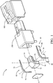
- Figure 1 shows an exploded view of the electrical connector 1.
- a connector housing 100, a contact holder 10, a shield body 200 and two pin-shaped contact elements 60 are shown.
- the contact holder 10, the shield body 200 and the connector housing 100 are shown along a plug axis X of the electrical connector 1.
- the electrically conductive shield body 200 surrounds the contact holder 10, around the plug axis X, at an angle of at least 180 ° around the plug axis when the electrical connector 1 is completely assembled.
- the pin-shaped contact elements 60 have a first contact area 66 at a first end and a second contact area 68 at a second end, with a middle area 64 extending between them.
- the first contact area 66 is aligned along the plug axis X of the electrical connector 1.
- the contact holder 10 has a recess 20 which extends from its surface 12 into the contact holder 10.
- the depression 20 is designed to receive and hold the central region 64 of a pin-shaped contact element 60.
- the depression 20 extends from a first contact holder end 16, which adjoins the first contact region 66, to a second contact holder end 18, which adjoins the second contact region 68.
- Figure 2 shows an exploded view of the contact holder 10 and the pin-shaped contact elements 60.
- the recess 20 has a U-shaped cross section.
- the central region 64 of the pin-shaped contact element 60 has a rectangular cross section.
- the central region 64 is shaped such that the second contact region 68 is aligned along a second axis Y, at right angles to the plug axis X.
- the central region 64 of the pin-shaped contact element 60 is formed by a first straight section 72, a second straight section 74 and a third straight section 76.
- the first straight section 72 and the second straight section 74 have an angle greater than 90 ° to one another and the second straight section 74 and the third straight section 76 have an angle greater than 90 ° to one another.
- Figure 3 shows a perspective view of the contact holder and the pin-shaped contact elements in the assembled state.
- the depression 20 extends at least so deep into the contact holder 10 that the central region 64 of the pin-shaped contact element 60 does not protrude beyond the surface 12 of the contact holder 10 from the depression 20, neither at right angles to the plug axis X nor at right angles to the second axis Y.
- the first contact region 66 of the pin-shaped contact element 60 is designed to be electrically connected to a complementary contact element of a complementary electrical connector.
- the second contact area 68 of the pin-shaped contact element 60 is designed to be electrically connected to an electrical circuit board.
- the two depressions 20 which the contact holder 10 have extend from the opposite regions of the surface 12 of the contact holder 10 towards one another.
- the depressions 20 run in a first plane A1, which is spanned by the plug-in axis X and the second axis Y.
- the wells 20 run parallel to one another from a first contact holder end 16, which adjoins the first contact region 66, to a second contact holder end 18, which adjoins the second contact region 68.
- the depressions 20 extend along a third axis Z from the surface 12 towards one another.
- the third axis Z is arranged at right angles to the plug axis X and at right angles to the second axis Y.
- the two pin-shaped contact elements 60 are held in the two depressions 20.
- the pin-shaped contact elements 60 are arranged parallel and spaced apart from one another in the first plane A1.
- the contact holder 10 is mirror-symmetrical in relation to the first plane A1 and the pin-shaped contact elements 60 are mirror-symmetrical in relation to the first plane A1.
Landscapes
- Coupling Device And Connection With Printed Circuit (AREA)
- Details Of Connecting Devices For Male And Female Coupling (AREA)
Abstract
Description
- Die Erfindung betrifft einen elektrischen Stecker zur Verwendung in Applikationen für High-Speed Datenübertragung sowie ein Verfahren zur Herstellung des elektrischen Steckers.
- Die Weiterentwicklung der Kraftfahrzeugtechnik hin zu autonom fahrenden, elektrisch angetriebenen Fahrzeugen, stellt neue Herausforderungen an die Fahrzeugverdrahtung und ebenso an die verwendeten elektrischen Stecker. Durch die neuen Herausforderungen wird auch eine Weiterentwicklung der Produktionstechnik für diese Komponenten notwendig. Insbesondere bei elektrischen Steckern für High-Speed Datenübertragung sind geringe Toleranzen bei den Maßen der Bauteile einzuhalten. Des Weiteren müssen die Produktionskosten so gering wie möglich gehalten werden. Üblicherweise werden elektrische Stecker, die stiftförmigen Kontaktelemente enthalten, hergestellt, indem die stiftförmigen Kontaktelemente mit einem dielektrischen Material umgeben werden, um sie voneinander zu isolieren. Üblicherweise wird das dielektrische Material um die Kontaktelemente gespritzt, wobei ein Spritzgussverfahren eingesetzt wird. Ein anderes Verfahren benutzt vorgefertigte Kunststoffteile, durch die die Kontaktelemente hindurchgestochen werden. Diese Verfahren haben je nach Anwendungsfall sowohl vor als auch Nachteile. Nachteilig ist, dass diese Stecker vorgefertigt und danach zum vollständigen Zusammenbau weitertransportiert werden müssen. Ein weiterer Nachteil bei diesem Verfahren ist die mangelnde Flexibilität, da die Werkzeuge zur Herstellung der Kunststoffteile nicht einfach auf geänderte Anforderungen an der Geometrie der Kunststoffteile angepasst werden können.
- Bei elektrischen Steckern für Highspeed Anwendungen spielt die Geometrie sowie der Abstand zweier zusammengehöriger Kontaktelemente eine wesentliche Rolle. Ein elektrischer Stecker kann für höhere Datenraten eingesetzt werden in dem man den elektrischen Stecker durch Abschirmung der Kontaktelemente modifiziert. Durch diese Modifikation steigen allerdings auch die Kosten für den elektrischen Stecker. Eine zweite Möglichkeit die Bandbreite zu erhöhen, ist die Kontaktelemente räumlich etwas mehr voneinander weg anzuordnen. Diese Möglichkeit erfordert jedoch Änderungen bei den Kunststoffteilen des elektrischen Steckers.
- Die Aufgabe der Erfindung ist es, einen elektrischen Stecker bereitzustellen, der in Fahrzeugen als Verbindungselemente in High-Speed-Daten-netzen eingesetzt werden kann. Wobei der Stecker mechanisch robust sowie kostengünstig und flexibel herzustellen ist.
- Die Aufgabe wird durch den Gegenstand des Anspruchs 1 sowie durch das Verfahren nach Anspruch 15 gelöst.
- Insbesondere durch einen elektrischen Stecker umfassend ein Steckergehäuse, einen Kontakthalter und mindestens eines stiftförmigen Kontakt-elements. Der Kontakthalter ist im Steckergehäuse angeordnet. Das stiftförmige Kontaktelement weist an einem ersten Ende einen ersten Kontaktbereich und an einem zweiten Ende einen zweiten Kontaktbereich auf, dazwischen erstreckt sich ein mittlerer Bereich. Der erste Kontaktbereich ist entlang einer Steckachse des elektrischen Steckers ausgerichtet. Der Kontakthalter weist eine Vertiefung auf, die sich von seiner Oberfläche in den Kontakthalter hinein erstreckt. Die Vertiefung ist dazu ausgebildet den mittleren Bereich des stiftförmigen Kontaktelements aufzunehmen und zu halten.
- Sowie durch ein Verfahren zum Herstellen eines elektrischeren Steckers, umfassend die Verfahrensschritte:
- a) Bereitstellen eines Steckergehäuses, eines Kontakthalters und eines Kontaktelements, wobei das stiftförmige Kontaktelement an einem ersten Ende einen ersten Kontaktbereich und an einem zweiten Ende einen zweiten Kontaktbereich aufweist, wobei sich dazwischen ein mittlerer Bereich erstreckt. Der Kontakthalter weist eine Vertiefung auf, die sich von seiner Oberfläche in den Kontakthalter hinein erstreckt. Die Vertiefung ist dazu ausgebildet den mittleren Bereich des stiftförmigen Kontaktelements aufzunehmen und zu halten.
- b) Ausrichten des ersten Kontaktbereichs des Kontaktelements entlang der Steckachse.
- c) Einfügen des mittleren Bereichs, des stiftförmigen Kontaktelements in die Vertiefung des Kontakthalters, sodass der mittlere Bereich in der Vertiefung aufgenommen und gehalten ist.
- d) Einführen des Kontakthalters in das Steckergehäuse, sodass der Kontakthalter in dem Steckergehäuse aufgenommen und gehalten ist.
- Der erfinderischen Stecker kann flexibel an einer Maschine oder einem Arbeitsplatz aus seinen einzelnen Komponenten komplett zusammengebaut werden. An einer vollautomatischen Maschine können die Kontaktelemente in gegurteter Form, als lose Schüttung oder durch eine Station der Maschine, die die Kontaktelemente aus Draht herstellt, bereitgestellt werden. Die Kontaktelemente können seitlich in den Kontakthalter eingesetzt werden, was maschinell sehr einfach und schnell möglich ist. Der Kontakthalter kann in einer geraden Bewegung in das Steckergehäuse geschoben und dort befestigt werden.
- Vorteilhafte Ausbildungen der Erfindung sind den Unteransprüchen, der Beschreibung und der Zeichnung zu entnehmen.
- Gemäß einer Ausführungsform erstreckt sich die Vertiefung von einem ersten Kontakthalterende, das an den ersten Kontaktbereich angrenzt, bis zu einem zweiten Kontakthalterende, das an den zweiten Kontaktbereich angrenzt. Dadurch wird das stiftförmige Kontaktelement optimal in der korrekten Position gehalten.
- Bevorzugt weist die Vertiefung einen U-förmigen Querschnitt auf. Die Vertiefung mit einem U-förmigen Querschnitt auszuführen erleichtert die Produktion des Kontakthalters.
- Bevorzugt weist die Vertiefung einen rechteckigen Querschnitt auf und der mittlere Bereich des stiftförmigen Kontaktelements weist ebenso einen rechteckigen Querschnitt auf. Durch die rechteckige Ausführung der Querschnitte ist eine optimale Passform des stiftförmigen Kontaktelements in der Vertiefung gewährleistet. Ein Verdrehen des Kontaktelements ist nicht möglich.
- Bevorzugt weist der erste Kontaktbereich einen runden Querschnitt auf und der mittlere Bereich des stiftförmigen Kontaktelements einen rechteckigen Querschnitt. Einige Applikationen erfordern Kontaktbereiche mit einem runden Querschnitt. Dieses wird ermöglicht unter Beibehaltung der Vorteile eines mittleren Bereichs mit einem rechteckigen Querschnitt.
- Nach einer weiteren Ausführungsform ist der mittlere Bereich derart geformt, dass der zweite Kontaktbereich entlang einer zweiten Achse, rechtwinkelig zur Steckachse, ausgerichtet ist. Für Anwendungen bei denen der elektrische Stecker mit einer Seite an einer Leiterplatte befestigt werden soll, kann er gewinkelt ausgeführt werden. Bei diesen Anwendungen befindet sich die Steckbuchse häufig in einer Seitenwand eines Gehäuses wobei die Seitenwand rechtwinklig zu Leiterplatte angeordnet ist.
- Bevorzugt wird der mittlere Bereich des stiftförmigen Kontaktelements durch ein erstes gerades Teilstück, ein zweites gerades Teilstück und ein drittes gerades Teilstück gebildet, wobei das erste gerade Teilstück und das zweites gerades Teilstück einen Winkel größer als 90° zueinander aufweisen und das zweite gerade Teilstück und das dritte gerade Teilstück einen Winkel größer als 90° zueinander aufweisen. Um das stiftförmigen Kontaktelement um 90° zu verformen kann es einfach um 90° gebogen werden. Es hat sich aber bei Hochfrequenzanwendungen gezeigt, dass in mehreren Winkeln gebogene Kontaktelemente einen positiven Einfluss auf den Wellenwiderstand haben.
- Nach einer weiteren Ausführungsform erstreckt sich die Vertiefung zumindest so tief in den Kontakthalter hinein, dass der mittlere Bereich des stiftförmigen Kontaktelements, weder rechtwinklig zur Steckachse noch rechtwinklig zur zweiten Achse über die Oberfläche des Kontakthalters aus der Vertiefung herausragt. Wenn das stiftförmige Kontaktelement exakt in der Vertiefung geführt ist, ist gewährleistet, dass bei Hochfrequenzanwendungen keine unerwarteten störenden Effekte auftreten.
- Bevorzugt ist der erste Kontaktbereich des stiftförmigen Kontaktelements dazu ausgebildet mit einem komplementären Kontaktelement eines komplementären elektrischen Steckers elektrisch verbunden zu werden und der zweite Kontaktbereich des stiftförmigen Kontaktelements ist dazu ausgebildet mit einer elektrischen Leiterplatte elektrisch verbunden zu werden. Angepasste Kontaktbereiche beugen Problemen bei der Montage vor. Der erste Kontaktbereich ist daraufhin optimiert mit korrespondierenden Kontaktelementen eines komplementären Steckers verbunden zu werden. Der erste Kontaktbereich kann mit einem kontaktfördernden oder Korrosion vermeidendem Material beschichtet sein. Der zweite Kontaktbereich kann verzinnt sein um mit einer Leiterplatte verlötet zu werden.
- Bevorzugt umgibt ein elektrisch leitfähiger Schirmkörper den Kontakthalter, die Steckachse umlaufend, in einem Winkel von mindestens 180° um die Steckachse. Eine Schirmung kann vorgesehen werden um Störungen bei der Datenübertragung zu vermeiden.
- Nach einer weiteren Ausführungsform weist der Kontakthalter zwei Vertiefungen auf, wobei sich die Vertiefungen in einer ersten Ebene, die von der Steckachse und der zweiten Achse aufgespannt wird, parallel zueinander, von sich gegenüberliegenden Bereichen der Oberfläche, entlang einer dritten Achse, die rechtwinklig zur Steckachse und rechtwinklig zur zweiten Achse angeordnet ist, in den Kontakthalter hinein, aufeinander zu, erstrecken. Die Vertiefungen erstrecken sich von gegenüberliegenden Seiten des Kontakthalters in das Material des Kontakthalters. Daraus ergibt sich ein symmetrischer Aufbau, sodass die beiden stiftförmigen Kontaktelemente parallel zueinander gehalten werden. Dieses ist äußerst wichtig bei hochfrequenter Datenübertragung.
- Bevorzugt sind zwei stiftförmige Kontaktelemente in den zwei Vertiefungen gehalten, wobei die zwei stiftförmigen Kontaktelemente parallel und beabstandet voneinander, in der ersten Ebene angeordnet sind. Wie oben beschrieben ist der parallele Verlauf der stiftförmigen Kontaktelemente äußerst wichtig. Außerdem ist der Abstand, in dem die stiftförmigen Kontaktelemente beabstandet sind, wichtig für den Wellenwiderstand und somit die Übertragungsqualität des elektrischen Steckers.
- Bevorzugt ist der Kontakthalter spiegelsymmetrisch im Bezug zur ersten Ebene (A1) ausgebildet und die stiftförmigen Kontaktelemente sind spiegelsymmetrisch im Bezug zur ersten Ebene angeordnet. Ein symmetrischer Aufbau des Kontakthalters ermöglicht eine einfache Haltevorrichtung für die stiftförmigen Kontaktelemente und beugt Übertragungsproblemen vor.
- Bevorzugt erstreckt sich die Vertiefung weiter, entlang der dritten Achse in den Kontakthalter als der Durchmesser des stiftförmigen Kontaktelements erfordert. Die Vertiefungen können tiefer in den Kontakthalter eingebracht werden als es erforderlich wäre um den mittleren Bereich der stiftförmigen Kontaktelemente vollständig aufzunehmen. Dadurch können universelle Kontakthalter verwendet werden. Je nach Erfordernis der Übertragungsgeschwindigkeit können die stiftförmige Kontaktelemente so näher zueinander oder weiter entfernt angeordnet werden.
- Nachfolgend wird die Erfindung anhand einer vorteilhaften Ausführungsform rein beispielhaft unter Bezugnahme auf der beigefügten Zeichnung
beschrieben. Es zeigen: - Fig. 1
- zeigt eine Explosionsdarstellung des elektrischen Steckers.
- Fig. 2
- zeigt eine Explosionsdarstellung des Kontakthalters und der stiftförmigen Kontaktelemente.
- Fig. 3
- zeigt perspektivische Darstellung des Kontakthalters und der stiftförmigen Kontaktelemente im montierten Zustand.
-
Figur 1 zeigt eine Explosionsdarstellung des elektrischer Steckers 1. Dargestellt ist ein Steckergehäuse 100, ein Kontakthalter 10, ein Schirmkörper 200 und zwei stiftförmige Kontaktelemente 60. Der Kontakthalter 10, der Schirmkörper 200 und das Steckergehäuse 100 sind entlang einer Steckachse X des elektrischen Steckers 1 dargestellt. Es ist ersichtlich das der elektrisch leitfähiger Schirmkörper 200 den Kontakthalter 10, die Steckachse X umlaufend, in einem Winkel von mindestens 180° um die Steckachse umgibt, wenn der elektrische Stecker 1 komplett montiert ist. Die stiftförmigen Kontaktelemente 60 weisen an einem ersten Ende einen ersten Kontaktbereich 66 und an einem zweiten Ende einen zweiten Kontaktbereich 68 auf, dazwischen erstreckt sich ein mittlerer Bereich 64. Der erste Kontaktbereich 66 ist entlang der Steckachse X des elektrischen Steckers 1 ausgerichtet. Der Kontakthalter 10 weist eine Vertiefung 20 auf, die sich von seiner Oberfläche 12 in den Kontakthalter 10 hinein erstreckt. Die Vertiefung 20 ist dazu ausgebildet den mittleren Bereich 64 eines stiftförmigen Kontaktelements 60 aufzunehmen und zu halten. Die Vertiefung 20 erstreckt sich von einem ersten Kontakthalterende 16, das an den ersten Kontaktbereich 66 angrenzt, bis zu einem zweiten Kontakthalterende 18, dass an den zweiten Kontaktbereich 68 angrenzt. -
Figur 2 zeigt eine Explosionsdarstellung des Kontakthalters 10 und der stiftförmigen Kontaktelemente 60. Die Vertiefung 20 weist einen U-förmigen Querschnitt auf. Der mittlere Bereich 64 des stiftförmigen Kontaktelements 60 weist einen rechteckigen Querschnitt auf. Der mittlere Bereich 64 ist derart geformt, dass der zweite Kontaktbereich 68 entlang einer zweiten Achse Y, rechtwinkelig zur Steckachse X, ausgerichtet ist. Der mittlere Bereich 64 des stiftförmigen Kontaktelements 60 wird durch ein erstes gerades Teilstück 72, ein zweites gerades Teilstück 74 und ein drittes gerades Teilstück 76 gebildet. Das erste gerade Teilstück 72 und das zweites gerades Teilstück 74 weisen einen Winkel größer als 90° zueinander auf und das zweite gerade Teilstück 74 und das dritte gerade Teilstück 76 weisen einen Winkel größer als 90° zueinander auf. -
Figur 3 zeigt eine perspektivische Darstellung des Kontakthalters und der stiftförmigen Kontaktelemente im montierten Zustand. Die Vertiefung 20 erstreckt sich zumindest so tief in den Kontakthalter 10 hinein, dass der mittlere Bereich 64 des stiftförmigen Kontaktelements 60, weder rechtwinklig zur Steckachse X noch rechtwinklig zur zweiten Achse Y über die Oberfläche 12 des Kontakthalters 10 aus der Vertiefung 20 herausragt. Der erste Kontaktbereich 66 des stiftförmigen Kontaktelements 60 ist dazu ausgebildet mit einem komplementären Kontaktelement eines komplementären elektrischen Steckers elektrisch verbunden zu werden. Der zweite Kontaktbereich 68 des stiftförmigen Kontaktelements 60 ist dazu ausgebildet mit einer elektrischen Leiterplatte elektrisch verbunden zu werden. Die zwei Vertiefungen 20 die der Kontakthalter 10 aufweist, erstrecken sich von den gegenüberliegenden Bereichen der Oberfläche 12 des Kontakthalters 10 aufeinander zu. Die Vertiefungen 20 verlaufen in einer ersten Ebene A1, die von der Steckachse X und der zweiten Achse Y aufgespannt wird. Die Vertiefungen 20 verlaufen parallel zueinander von einem ersten Kontakthalterende 16, das an den ersten Kontaktbereich 66 angrenzt, bis zu einem zweiten Kontakthalterende 18, dass an den zweiten Kontaktbereich 68 angrenzt. Die Vertiefungen 20 erstrecken sich entlang einer dritten Achse Z von der Oberfläche 12 aufeinander zu. Die dritte Achse Z ist rechtwinklig zur Steckachse X und rechtwinklig zur zweiten Achse Y angeordnet. Die zwei stiftförmigen Kontaktelemente 60 sind in den zwei Vertiefungen 20 gehalten. Die stiftförmigen Kontaktelemente 60 sind parallel und beabstandet voneinander, in der ersten Ebene A1 angeordnet. Der Kontakthalter 10 ist spiegelsymmetrisch im Bezug zur ersten Ebene A1 ausgebildet und die stiftförmigen Kontaktelemente 60 sind spiegelsymmetrisch im Bezug zur ersten Ebene A1 angeordnet.
Claims (15)
- Elektrischer Stecker (1) umfassend ein Steckergehäuse (100), einen Kontakthalter (10) und mindestens einen stiftförmiges Kontaktelement (60), wobei der Kontakthalter (10) im Steckergehäuse (100) angeordnet ist, wobei das stiftförmige Kontaktelement (60) an einem ersten Ende einen ersten Kontaktbereich (66) und an einem zweiten Ende einen zweiten Kontaktbereich (68) aufweist, wobei sich dazwischen ein mittlere Bereich (64) erstreckt, der erste Kontaktbereich (66) ist entlang einer Steckachse (X) des elektrischen Steckers (1) ausgerichtet, wobei der Kontakthalter (10) eine Vertiefung (20), die sich von seiner Oberfläche (12) in den Kontakthalter (10) hinein erstreckt, aufweist, wobei die Vertiefung (20) dazu ausgebildet ist den mittleren Bereich (64) des stiftförmigen Kontaktelements (60) aufzunehmen und zu halten.
- Elektrischer Stecker (1) nach Anspruch 1, wobei sich die Vertiefung (20) von einem ersten Kontakthalterende (16), das an den ersten Kontaktbereich (66) angrenzt, bis zu einem zweiten Kontakthalterende (18), dass an den zweiten Kontaktbereich (68) angrenzt, erstreckt.
- Elektrischer Stecker (1) nach einem der vorhergehenden Ansprüche, wobei die Vertiefung (20) einen U-förmigen Querschnitt aufweist.
- Elektrischer Stecker (1) nach Anspruch 3, wobei die Vertiefung (20) einen rechteckigen Querschnitt aufweist und der mittlere Bereich (64) des stiftförmigen Kontaktelements (60) einen rechteckigen Querschnitt aufweist.
- Elektrischer Stecker (1) nach einem der Ansprüche 1-3, wobei der erste Kontaktbereich (66) einen runden Querschnitt aufweist und der mittlere Bereich (64) des stiftförmigen Kontaktelements (60) einen rechteckigen Querschnitt aufweist.
- Elektrischer Stecker (1) nach einem der vorhergehenden Ansprüche, wobei der mittlere Bereich (64) derart geformt ist, dass der zweite Kontaktbereich (68) entlang einer zweiten Achse (Y), rechtwinkelig zur Steckachse (X), ausgerichtet ist.
- Elektrischer Stecker (1) nach einem der vorhergehenden Ansprüche, wobei, der mittlere Bereich (64) des stiftförmigen Kontaktelements (60) durch ein erstes gerades Teilstück (72), ein zweites gerades Teilstück (74) und ein drittes gerades Teilstück (76) gebildet wird, wobei das erste gerade Teilstück (72) und das zweites gerades Teilstück (74) einen Winkel größer als 90° zueinander aufweisen und das zweite gerade Teilstück (74) und das dritte gerade Teilstück (76) einen Winkel größer als 90° zueinander aufweisen.
- Elektrischer Stecker (1) nach einem der Ansprüche 6-7, wobei die Vertiefung (20) sich zumindest so tief in den Kontakthalter (10) hi-nein erstreckt, dass der mittlere Bereich (64) des stiftförmigen Kontaktelements (60), weder rechtwinklig zur Steckachse (X) noch rechtwinklig zur zweiten Achse (Y) über die Oberfläche (12) des Kontakthalters (10) aus der Vertiefung (20) herausragt.
- Elektrischer Stecker (1) nach einem der vorhergehenden Ansprüche, wobei der erste Kontaktbereich (66) des stiftförmigen Kontaktelements (60) dazu ausgebildet ist mit einem komplementären Kontaktelement eines komplementären elektrischen Steckers elektrisch verbunden zu werden und wobei der zweite Kontaktbereich (68) des stiftförmigen Kontaktelements (60) dazu ausgebildet ist mit einer elektrischen Leiterplatte elektrisch verbunden zu werden.
- Elektrischer Stecker (1) nach einem der vorhergehenden Ansprüche, wobei, ein elektrisch leitfähiger Schirmkörper (200) den Kontakthalter (10), die Steckachse (X) umlaufend, in einem Winkel von mindestens 180° um die Steckachse (X), umgibt.
- Elektrischer Stecker (1) nach einem der vorhergehenden Ansprüche, wobei, der Kontakthalter (10) zwei Vertiefungen (20) aufweist, wobei die Vertiefungen (20) in einer ersten Ebene (A1), die von der Steckachse (X) und der zweiten Achse (Y) aufgespannt wird, parallel zueinander, von sich gegenüberliegenden Bereichen der Oberfläche (12), entlang einer dritten Achse (Z), die rechtwinklig zur Steckachse (X) und rechtwinklig zur zweiten Achse (Y) angeordnet ist, in den Kontakthalter (10) hinein, aufeinander zu, erstrecken.
- Elektrischer Stecker (1) nach Anspruch 11, wobei, zwei stiftförmigen Kontaktelemente (60) in den zwei Vertiefungen (20) gehalten sind, wobei die zwei stiftförmigen Kontaktelemente (60) parallel und beabstandet voneinander, in der ersten Ebene (A1) angeordnet sind.
- Elektrischer Stecker (1) nach einem der Ansprüche 11-12, wobei der Kontakthalter (10) spiegelsymmetrisch im Bezug zur ersten Ebene (A1) ausgebildet ist und wobei die stiftförmigen Kontaktelemente (60) spiegelsymmetrisch im Bezug zur ersten Ebene (A1) angeordnet sind.
- Elektrischer Stecker (1) nach einem der Ansprüche 11-13, wobei sich die Vertiefung (20) weiter, entlang der dritten Achse (Z) in den Kontakthalter (10) erstreckt als der Durchmesser des stiftförmigen Kontaktelements (60) erfordert.
- Verfahren zum Herstellen eines elektrischeren Steckers (1), umfassend die Verfahrensschritte:a) bereitstellen eines Steckergehäuses (100), eines Kontakthalters (10) und eines Kontaktelements (60), wobei das stiftförmige Kontaktelement (60) an einem ersten Ende einen ersten Kontaktbereich (66) und an einem zweiten Ende einen zweiten Kontaktbereich (68) aufweist, wobei sich dazwischen ein mittlere Bereich (64) erstreckt, wobei der Kontakthalter (10) eine Vertiefung (20), die sich von seiner Oberfläche (12) in den Kontakthalter (10) hinein erstreckt, aufweist, wobei die Vertiefung (20) dazu ausgebildet ist den mittleren Bereich (64) des stiftförmigen Kontaktelements (60) aufzunehmen und zu halten;b) ausrichten des ersten Kontaktbereichs (66) des Kontaktelements (60) entlang der Steckachse (X),c) Einfügen des mittleren Bereichs (64), des stiftförmigen Kontaktelements (60) in die Vertiefung (20) des Kontakthalters (10), sodass der mittlere Bereich (64) in der Vertiefung (20) aufgenommen und gehalten ist;d) Einführen des Kontakthalters (10) in das Steckergehäuse (100), sodass der Kontakthalter (10) in dem Steckergehäuse (100) aufgenommen und gehalten ist.
Priority Applications (1)
| Application Number | Priority Date | Filing Date | Title |
|---|---|---|---|
| EP18190970.6A EP3618194B1 (de) | 2018-08-27 | 2018-08-27 | Elektrischer stecker |
Applications Claiming Priority (1)
| Application Number | Priority Date | Filing Date | Title |
|---|---|---|---|
| EP18190970.6A EP3618194B1 (de) | 2018-08-27 | 2018-08-27 | Elektrischer stecker |
Publications (2)
| Publication Number | Publication Date |
|---|---|
| EP3618194A1 true EP3618194A1 (de) | 2020-03-04 |
| EP3618194B1 EP3618194B1 (de) | 2024-10-02 |
Family
ID=63407121
Family Applications (1)
| Application Number | Title | Priority Date | Filing Date |
|---|---|---|---|
| EP18190970.6A Active EP3618194B1 (de) | 2018-08-27 | 2018-08-27 | Elektrischer stecker |
Country Status (1)
| Country | Link |
|---|---|
| EP (1) | EP3618194B1 (de) |
Cited By (3)
| Publication number | Priority date | Publication date | Assignee | Title |
|---|---|---|---|---|
| CN113839237A (zh) * | 2020-06-24 | 2021-12-24 | 罗森伯格高频技术有限及两合公司 | 电插头连接器和电连接装置 |
| EP4481960A1 (de) * | 2023-06-23 | 2024-12-25 | Mitsumi Electric Co., Ltd. | Elektrischer verbinder und verfahren zur herstellung eines kontaktstifts eines elektrischen verbinders |
| US12482995B2 (en) | 2022-07-13 | 2025-11-25 | Fuding Precision Components (Shenzhen) Co., Ltd. | Electrical connector with a positively retained metallic cover |
Citations (3)
| Publication number | Priority date | Publication date | Assignee | Title |
|---|---|---|---|---|
| EP0242318A1 (de) * | 1986-04-10 | 1987-10-21 | UNITED TECHNOLOGIES AUTOMOTIVE, Inc. | Anordnung zum Sichern eines elektrischen Steckers in einem Steckergehäuse |
| US5071372A (en) * | 1990-11-30 | 1991-12-10 | Amp Incorporated | Connector with contact spacer plate having tapered channels |
| US20140256189A1 (en) * | 2013-03-08 | 2014-09-11 | Kinsun Industries Inc. | Electrical connector |
-
2018
- 2018-08-27 EP EP18190970.6A patent/EP3618194B1/de active Active
Patent Citations (3)
| Publication number | Priority date | Publication date | Assignee | Title |
|---|---|---|---|---|
| EP0242318A1 (de) * | 1986-04-10 | 1987-10-21 | UNITED TECHNOLOGIES AUTOMOTIVE, Inc. | Anordnung zum Sichern eines elektrischen Steckers in einem Steckergehäuse |
| US5071372A (en) * | 1990-11-30 | 1991-12-10 | Amp Incorporated | Connector with contact spacer plate having tapered channels |
| US20140256189A1 (en) * | 2013-03-08 | 2014-09-11 | Kinsun Industries Inc. | Electrical connector |
Cited By (5)
| Publication number | Priority date | Publication date | Assignee | Title |
|---|---|---|---|---|
| CN113839237A (zh) * | 2020-06-24 | 2021-12-24 | 罗森伯格高频技术有限及两合公司 | 电插头连接器和电连接装置 |
| EP3930111A1 (de) * | 2020-06-24 | 2021-12-29 | Rosenberger Hochfrequenztechnik GmbH & Co. KG | Elektrischer steckverbinder und elektrische verbindungsanordnung |
| US11855394B2 (en) | 2020-06-24 | 2023-12-26 | Rosenberger Hochfrequenztechnik Gmbh & Co. Kg | Electrical plug connector and electrical connecting arrangement |
| US12482995B2 (en) | 2022-07-13 | 2025-11-25 | Fuding Precision Components (Shenzhen) Co., Ltd. | Electrical connector with a positively retained metallic cover |
| EP4481960A1 (de) * | 2023-06-23 | 2024-12-25 | Mitsumi Electric Co., Ltd. | Elektrischer verbinder und verfahren zur herstellung eines kontaktstifts eines elektrischen verbinders |
Also Published As
| Publication number | Publication date |
|---|---|
| EP3618194B1 (de) | 2024-10-02 |
Similar Documents
| Publication | Publication Date | Title |
|---|---|---|
| DE112007002161B4 (de) | Steckverbindung | |
| DE102008006340A1 (de) | Steckverbindungsanordnung mit aufgeformtem abgeschirmtem Gehäuse | |
| DE102006023979A1 (de) | Steckverbinder, Buchsenverbinder und elektrisches Verbindungsgerät | |
| EP1263091A2 (de) | Neunzig-Grad-drehbarer Steckverbinder | |
| DE202015005683U1 (de) | Elektrischer Stecker | |
| DE102017123080A1 (de) | Elektrischer Steckverbinder und Verfahren zur Montage eines elektrischen Steckverbinders | |
| DE102012105256A1 (de) | Isolierkörper eines Steckverbinders | |
| DE102017127382A1 (de) | Elektrischer verbinder und damit ausgestattete elektrische leitungsanordnung | |
| EP3618194B1 (de) | Elektrischer stecker | |
| DE102006043574A1 (de) | Solarsteckverbinder mit verbesserten Rastmitteln | |
| DE102011001714A1 (de) | Querbrücker für eine elektrische Klemme | |
| EP1959523A1 (de) | Kodiereinrichtung für Steckverbinder | |
| DE102009039087A1 (de) | Verbindungsanordnung für elektrische Baugruppen | |
| EP2862243A1 (de) | Isolierkörper eines steckverbinders | |
| EP2724422A1 (de) | Stecker und verfahren zu dessen herstellung | |
| DE102005023977A1 (de) | Stift, Vorrichtung und Verfahren | |
| DE1615655A1 (de) | Elektrisches Steckergehaeuse | |
| DE102013013715B4 (de) | Elektrische Kontaktanordnung sowie Verfahren zum Herstellen einer solchen elektrischen Kontaktanordnung | |
| EP2026416B1 (de) | Kabelaufnahmevorrichtung und Kontaktsystem | |
| DE102014115384A1 (de) | Prüfkabel sowie Buchsenadapter für ein Prüfkabel | |
| DE102019106817A1 (de) | Staubvermeidungsabdeckung und stecker | |
| DE112018003477T5 (de) | Stecker und Steckeranordnung | |
| DE102011120056B4 (de) | Steckverbindung für eine Platine | |
| DE102010000822A1 (de) | Drahtverbindungseinheit | |
| DE102019118141A1 (de) | Kabelverbinder für einen elektrischen Parkbremsaktor |
Legal Events
| Date | Code | Title | Description |
|---|---|---|---|
| PUAI | Public reference made under article 153(3) epc to a published international application that has entered the european phase |
Free format text: ORIGINAL CODE: 0009012 |
|
| STAA | Information on the status of an ep patent application or granted ep patent |
Free format text: STATUS: THE APPLICATION HAS BEEN PUBLISHED |
|
| AK | Designated contracting states |
Kind code of ref document: A1 Designated state(s): AL AT BE BG CH CY CZ DE DK EE ES FI FR GB GR HR HU IE IS IT LI LT LU LV MC MK MT NL NO PL PT RO RS SE SI SK SM TR |
|
| AX | Request for extension of the european patent |
Extension state: BA ME |
|
| STAA | Information on the status of an ep patent application or granted ep patent |
Free format text: STATUS: REQUEST FOR EXAMINATION WAS MADE |
|
| 17P | Request for examination filed |
Effective date: 20200902 |
|
| RBV | Designated contracting states (corrected) |
Designated state(s): AL AT BE BG CH CY CZ DE DK EE ES FI FR GB GR HR HU IE IS IT LI LT LU LV MC MK MT NL NO PL PT RO RS SE SI SK SM TR |
|
| STAA | Information on the status of an ep patent application or granted ep patent |
Free format text: STATUS: EXAMINATION IS IN PROGRESS |
|
| 17Q | First examination report despatched |
Effective date: 20210824 |
|
| RAP3 | Party data changed (applicant data changed or rights of an application transferred) |
Owner name: APTIV TECHNOLOGIES LIMITED |
|
| GRAP | Despatch of communication of intention to grant a patent |
Free format text: ORIGINAL CODE: EPIDOSNIGR1 |
|
| STAA | Information on the status of an ep patent application or granted ep patent |
Free format text: STATUS: GRANT OF PATENT IS INTENDED |
|
| RIC1 | Information provided on ipc code assigned before grant |
Ipc: H01R 13/506 20060101ALN20240321BHEP Ipc: H01R 12/72 20110101ALN20240321BHEP Ipc: H01R 13/41 20060101AFI20240321BHEP |
|
| INTG | Intention to grant announced |
Effective date: 20240408 |
|
| RAP1 | Party data changed (applicant data changed or rights of an application transferred) |
Owner name: APTIV TECHNOLOGIES AG |
|
| RIC1 | Information provided on ipc code assigned before grant |
Ipc: H01R 13/506 20060101ALN20240322BHEP Ipc: H01R 12/72 20110101ALN20240322BHEP Ipc: H01R 13/41 20060101AFI20240322BHEP |
|
| GRAS | Grant fee paid |
Free format text: ORIGINAL CODE: EPIDOSNIGR3 |
|
| GRAA | (expected) grant |
Free format text: ORIGINAL CODE: 0009210 |
|
| STAA | Information on the status of an ep patent application or granted ep patent |
Free format text: STATUS: THE PATENT HAS BEEN GRANTED |
|
| P01 | Opt-out of the competence of the unified patent court (upc) registered |
Free format text: CASE NUMBER: APP_44854/2024 Effective date: 20240801 |
|
| RAP3 | Party data changed (applicant data changed or rights of an application transferred) |
Owner name: APTIV TECHNOLOGIES AG |
|
| AK | Designated contracting states |
Kind code of ref document: B1 Designated state(s): AL AT BE BG CH CY CZ DE DK EE ES FI FR GB GR HR HU IE IS IT LI LT LU LV MC MK MT NL NO PL PT RO RS SE SI SK SM TR |
|
| REG | Reference to a national code |
Ref country code: GB Ref legal event code: FG4D Free format text: NOT ENGLISH |
|
| REG | Reference to a national code |
Ref country code: CH Ref legal event code: EP |
|
| REG | Reference to a national code |
Ref country code: DE Ref legal event code: R096 Ref document number: 502018015180 Country of ref document: DE |
|
| REG | Reference to a national code |
Ref country code: IE Ref legal event code: FG4D Free format text: LANGUAGE OF EP DOCUMENT: GERMAN |
|
| REG | Reference to a national code |
Ref country code: LT Ref legal event code: MG9D |
|
| REG | Reference to a national code |
Ref country code: NL Ref legal event code: MP Effective date: 20241002 |
|
| PG25 | Lapsed in a contracting state [announced via postgrant information from national office to epo] |
Ref country code: NL Free format text: LAPSE BECAUSE OF FAILURE TO SUBMIT A TRANSLATION OF THE DESCRIPTION OR TO PAY THE FEE WITHIN THE PRESCRIBED TIME-LIMIT Effective date: 20241002 |
|
| PG25 | Lapsed in a contracting state [announced via postgrant information from national office to epo] |
Ref country code: NL Free format text: LAPSE BECAUSE OF FAILURE TO SUBMIT A TRANSLATION OF THE DESCRIPTION OR TO PAY THE FEE WITHIN THE PRESCRIBED TIME-LIMIT Effective date: 20241002 |
|
| PG25 | Lapsed in a contracting state [announced via postgrant information from national office to epo] |
Ref country code: IS Free format text: LAPSE BECAUSE OF FAILURE TO SUBMIT A TRANSLATION OF THE DESCRIPTION OR TO PAY THE FEE WITHIN THE PRESCRIBED TIME-LIMIT Effective date: 20250202 Ref country code: PT Free format text: LAPSE BECAUSE OF FAILURE TO SUBMIT A TRANSLATION OF THE DESCRIPTION OR TO PAY THE FEE WITHIN THE PRESCRIBED TIME-LIMIT Effective date: 20250203 Ref country code: HR Free format text: LAPSE BECAUSE OF FAILURE TO SUBMIT A TRANSLATION OF THE DESCRIPTION OR TO PAY THE FEE WITHIN THE PRESCRIBED TIME-LIMIT Effective date: 20241002 |
|
| PG25 | Lapsed in a contracting state [announced via postgrant information from national office to epo] |
Ref country code: FI Free format text: LAPSE BECAUSE OF FAILURE TO SUBMIT A TRANSLATION OF THE DESCRIPTION OR TO PAY THE FEE WITHIN THE PRESCRIBED TIME-LIMIT Effective date: 20241002 |
|
| PG25 | Lapsed in a contracting state [announced via postgrant information from national office to epo] |
Ref country code: BG Free format text: LAPSE BECAUSE OF FAILURE TO SUBMIT A TRANSLATION OF THE DESCRIPTION OR TO PAY THE FEE WITHIN THE PRESCRIBED TIME-LIMIT Effective date: 20241002 |
|
| PG25 | Lapsed in a contracting state [announced via postgrant information from national office to epo] |
Ref country code: ES Free format text: LAPSE BECAUSE OF FAILURE TO SUBMIT A TRANSLATION OF THE DESCRIPTION OR TO PAY THE FEE WITHIN THE PRESCRIBED TIME-LIMIT Effective date: 20241002 |
|
| PG25 | Lapsed in a contracting state [announced via postgrant information from national office to epo] |
Ref country code: NO Free format text: LAPSE BECAUSE OF FAILURE TO SUBMIT A TRANSLATION OF THE DESCRIPTION OR TO PAY THE FEE WITHIN THE PRESCRIBED TIME-LIMIT Effective date: 20250102 |
|
| PG25 | Lapsed in a contracting state [announced via postgrant information from national office to epo] |
Ref country code: LV Free format text: LAPSE BECAUSE OF FAILURE TO SUBMIT A TRANSLATION OF THE DESCRIPTION OR TO PAY THE FEE WITHIN THE PRESCRIBED TIME-LIMIT Effective date: 20241002 Ref country code: GR Free format text: LAPSE BECAUSE OF FAILURE TO SUBMIT A TRANSLATION OF THE DESCRIPTION OR TO PAY THE FEE WITHIN THE PRESCRIBED TIME-LIMIT Effective date: 20250103 |
|
| PG25 | Lapsed in a contracting state [announced via postgrant information from national office to epo] |
Ref country code: PL Free format text: LAPSE BECAUSE OF FAILURE TO SUBMIT A TRANSLATION OF THE DESCRIPTION OR TO PAY THE FEE WITHIN THE PRESCRIBED TIME-LIMIT Effective date: 20241002 Ref country code: CZ Free format text: LAPSE BECAUSE OF FAILURE TO SUBMIT A TRANSLATION OF THE DESCRIPTION OR TO PAY THE FEE WITHIN THE PRESCRIBED TIME-LIMIT Effective date: 20241002 |
|
| PG25 | Lapsed in a contracting state [announced via postgrant information from national office to epo] |
Ref country code: RS Free format text: LAPSE BECAUSE OF FAILURE TO SUBMIT A TRANSLATION OF THE DESCRIPTION OR TO PAY THE FEE WITHIN THE PRESCRIBED TIME-LIMIT Effective date: 20250102 |
|
| PG25 | Lapsed in a contracting state [announced via postgrant information from national office to epo] |
Ref country code: SM Free format text: LAPSE BECAUSE OF FAILURE TO SUBMIT A TRANSLATION OF THE DESCRIPTION OR TO PAY THE FEE WITHIN THE PRESCRIBED TIME-LIMIT Effective date: 20241002 |
|
| REG | Reference to a national code |
Ref country code: DE Ref legal event code: R097 Ref document number: 502018015180 Country of ref document: DE |
|
| PG25 | Lapsed in a contracting state [announced via postgrant information from national office to epo] |
Ref country code: DK Free format text: LAPSE BECAUSE OF FAILURE TO SUBMIT A TRANSLATION OF THE DESCRIPTION OR TO PAY THE FEE WITHIN THE PRESCRIBED TIME-LIMIT Effective date: 20241002 |
|
| PG25 | Lapsed in a contracting state [announced via postgrant information from national office to epo] |
Ref country code: EE Free format text: LAPSE BECAUSE OF FAILURE TO SUBMIT A TRANSLATION OF THE DESCRIPTION OR TO PAY THE FEE WITHIN THE PRESCRIBED TIME-LIMIT Effective date: 20241002 |
|
| PG25 | Lapsed in a contracting state [announced via postgrant information from national office to epo] |
Ref country code: RO Free format text: LAPSE BECAUSE OF FAILURE TO SUBMIT A TRANSLATION OF THE DESCRIPTION OR TO PAY THE FEE WITHIN THE PRESCRIBED TIME-LIMIT Effective date: 20241002 |
|
| PG25 | Lapsed in a contracting state [announced via postgrant information from national office to epo] |
Ref country code: SK Free format text: LAPSE BECAUSE OF FAILURE TO SUBMIT A TRANSLATION OF THE DESCRIPTION OR TO PAY THE FEE WITHIN THE PRESCRIBED TIME-LIMIT Effective date: 20241002 |
|
| PG25 | Lapsed in a contracting state [announced via postgrant information from national office to epo] |
Ref country code: IT Free format text: LAPSE BECAUSE OF FAILURE TO SUBMIT A TRANSLATION OF THE DESCRIPTION OR TO PAY THE FEE WITHIN THE PRESCRIBED TIME-LIMIT Effective date: 20241002 |
|
| PLBE | No opposition filed within time limit |
Free format text: ORIGINAL CODE: 0009261 |
|
| STAA | Information on the status of an ep patent application or granted ep patent |
Free format text: STATUS: NO OPPOSITION FILED WITHIN TIME LIMIT |
|
| PG25 | Lapsed in a contracting state [announced via postgrant information from national office to epo] |
Ref country code: SE Free format text: LAPSE BECAUSE OF FAILURE TO SUBMIT A TRANSLATION OF THE DESCRIPTION OR TO PAY THE FEE WITHIN THE PRESCRIBED TIME-LIMIT Effective date: 20241002 |
|
| 26N | No opposition filed |
Effective date: 20250703 |
|
| PGFP | Annual fee paid to national office [announced via postgrant information from national office to epo] |
Ref country code: DE Payment date: 20250722 Year of fee payment: 8 |
|
| PGFP | Annual fee paid to national office [announced via postgrant information from national office to epo] |
Ref country code: GB Payment date: 20250813 Year of fee payment: 8 |
|
| PGFP | Annual fee paid to national office [announced via postgrant information from national office to epo] |
Ref country code: FR Payment date: 20250812 Year of fee payment: 8 |
|
| REG | Reference to a national code |
Ref country code: CH Ref legal event code: H13 Free format text: ST27 STATUS EVENT CODE: U-0-0-H10-H13 (AS PROVIDED BY THE NATIONAL OFFICE) Effective date: 20260324 |
|
| PG25 | Lapsed in a contracting state [announced via postgrant information from national office to epo] |
Ref country code: MC Free format text: LAPSE BECAUSE OF FAILURE TO SUBMIT A TRANSLATION OF THE DESCRIPTION OR TO PAY THE FEE WITHIN THE PRESCRIBED TIME-LIMIT Effective date: 20241002 |
|
| PG25 | Lapsed in a contracting state [announced via postgrant information from national office to epo] |
Ref country code: LU Free format text: LAPSE BECAUSE OF NON-PAYMENT OF DUE FEES Effective date: 20250827 |
|
| PG25 | Lapsed in a contracting state [announced via postgrant information from national office to epo] |
Ref country code: CH Free format text: LAPSE BECAUSE OF NON-PAYMENT OF DUE FEES Effective date: 20250831 |