EP3598518B1 - Organische lichtemittierende vorrichtung - Google Patents
Organische lichtemittierende vorrichtung Download PDFInfo
- Publication number
- EP3598518B1 EP3598518B1 EP19168054.5A EP19168054A EP3598518B1 EP 3598518 B1 EP3598518 B1 EP 3598518B1 EP 19168054 A EP19168054 A EP 19168054A EP 3598518 B1 EP3598518 B1 EP 3598518B1
- Authority
- EP
- European Patent Office
- Prior art keywords
- group
- compound
- substituted
- unsubstituted
- independently
- Prior art date
- Legal status (The legal status is an assumption and is not a legal conclusion. Google has not performed a legal analysis and makes no representation as to the accuracy of the status listed.)
- Active
Links
Images




Classifications
-
- H—ELECTRICITY
- H10—SEMICONDUCTOR DEVICES; ELECTRIC SOLID-STATE DEVICES NOT OTHERWISE PROVIDED FOR
- H10K—ORGANIC ELECTRIC SOLID-STATE DEVICES
- H10K50/00—Organic light-emitting devices
- H10K50/10—OLEDs or polymer light-emitting diodes [PLED]
- H10K50/11—OLEDs or polymer light-emitting diodes [PLED] characterised by the electroluminescent [EL] layers
- H10K50/125—OLEDs or polymer light-emitting diodes [PLED] characterised by the electroluminescent [EL] layers specially adapted for multicolour light emission, e.g. for emitting white light
-
- H—ELECTRICITY
- H10—SEMICONDUCTOR DEVICES; ELECTRIC SOLID-STATE DEVICES NOT OTHERWISE PROVIDED FOR
- H10K—ORGANIC ELECTRIC SOLID-STATE DEVICES
- H10K50/00—Organic light-emitting devices
- H10K50/10—OLEDs or polymer light-emitting diodes [PLED]
- H10K50/11—OLEDs or polymer light-emitting diodes [PLED] characterised by the electroluminescent [EL] layers
-
- H—ELECTRICITY
- H10—SEMICONDUCTOR DEVICES; ELECTRIC SOLID-STATE DEVICES NOT OTHERWISE PROVIDED FOR
- H10K—ORGANIC ELECTRIC SOLID-STATE DEVICES
- H10K50/00—Organic light-emitting devices
- H10K50/10—OLEDs or polymer light-emitting diodes [PLED]
- H10K50/11—OLEDs or polymer light-emitting diodes [PLED] characterised by the electroluminescent [EL] layers
- H10K50/125—OLEDs or polymer light-emitting diodes [PLED] characterised by the electroluminescent [EL] layers specially adapted for multicolour light emission, e.g. for emitting white light
- H10K50/13—OLEDs or polymer light-emitting diodes [PLED] characterised by the electroluminescent [EL] layers specially adapted for multicolour light emission, e.g. for emitting white light comprising stacked EL layers within one EL unit
-
- H—ELECTRICITY
- H10—SEMICONDUCTOR DEVICES; ELECTRIC SOLID-STATE DEVICES NOT OTHERWISE PROVIDED FOR
- H10K—ORGANIC ELECTRIC SOLID-STATE DEVICES
- H10K50/00—Organic light-emitting devices
- H10K50/10—OLEDs or polymer light-emitting diodes [PLED]
- H10K50/17—Carrier injection layers
- H10K50/171—Electron injection layers
-
- H—ELECTRICITY
- H10—SEMICONDUCTOR DEVICES; ELECTRIC SOLID-STATE DEVICES NOT OTHERWISE PROVIDED FOR
- H10K—ORGANIC ELECTRIC SOLID-STATE DEVICES
- H10K50/00—Organic light-emitting devices
- H10K50/10—OLEDs or polymer light-emitting diodes [PLED]
- H10K50/18—Carrier blocking layers
-
- H—ELECTRICITY
- H10—SEMICONDUCTOR DEVICES; ELECTRIC SOLID-STATE DEVICES NOT OTHERWISE PROVIDED FOR
- H10K—ORGANIC ELECTRIC SOLID-STATE DEVICES
- H10K50/00—Organic light-emitting devices
- H10K50/10—OLEDs or polymer light-emitting diodes [PLED]
- H10K50/19—Tandem OLEDs
-
- H—ELECTRICITY
- H10—SEMICONDUCTOR DEVICES; ELECTRIC SOLID-STATE DEVICES NOT OTHERWISE PROVIDED FOR
- H10K—ORGANIC ELECTRIC SOLID-STATE DEVICES
- H10K85/00—Organic materials used in the body or electrodes of devices covered by this subclass
- H10K85/30—Coordination compounds
- H10K85/341—Transition metal complexes, e.g. Ru(II)polypyridine complexes
- H10K85/342—Transition metal complexes, e.g. Ru(II)polypyridine complexes comprising iridium
-
- H—ELECTRICITY
- H10—SEMICONDUCTOR DEVICES; ELECTRIC SOLID-STATE DEVICES NOT OTHERWISE PROVIDED FOR
- H10K—ORGANIC ELECTRIC SOLID-STATE DEVICES
- H10K85/00—Organic materials used in the body or electrodes of devices covered by this subclass
- H10K85/60—Organic compounds having low molecular weight
- H10K85/615—Polycyclic condensed aromatic hydrocarbons, e.g. anthracene
- H10K85/622—Polycyclic condensed aromatic hydrocarbons, e.g. anthracene containing four rings, e.g. pyrene
-
- H—ELECTRICITY
- H10—SEMICONDUCTOR DEVICES; ELECTRIC SOLID-STATE DEVICES NOT OTHERWISE PROVIDED FOR
- H10K—ORGANIC ELECTRIC SOLID-STATE DEVICES
- H10K85/00—Organic materials used in the body or electrodes of devices covered by this subclass
- H10K85/60—Organic compounds having low molecular weight
- H10K85/615—Polycyclic condensed aromatic hydrocarbons, e.g. anthracene
- H10K85/626—Polycyclic condensed aromatic hydrocarbons, e.g. anthracene containing more than one polycyclic condensed aromatic rings, e.g. bis-anthracene
-
- H—ELECTRICITY
- H10—SEMICONDUCTOR DEVICES; ELECTRIC SOLID-STATE DEVICES NOT OTHERWISE PROVIDED FOR
- H10K—ORGANIC ELECTRIC SOLID-STATE DEVICES
- H10K85/00—Organic materials used in the body or electrodes of devices covered by this subclass
- H10K85/60—Organic compounds having low molecular weight
- H10K85/631—Amine compounds having at least two aryl rest on at least one amine-nitrogen atom, e.g. triphenylamine
- H10K85/633—Amine compounds having at least two aryl rest on at least one amine-nitrogen atom, e.g. triphenylamine comprising polycyclic condensed aromatic hydrocarbons as substituents on the nitrogen atom
-
- H—ELECTRICITY
- H10—SEMICONDUCTOR DEVICES; ELECTRIC SOLID-STATE DEVICES NOT OTHERWISE PROVIDED FOR
- H10K—ORGANIC ELECTRIC SOLID-STATE DEVICES
- H10K85/00—Organic materials used in the body or electrodes of devices covered by this subclass
- H10K85/60—Organic compounds having low molecular weight
- H10K85/649—Aromatic compounds comprising a hetero atom
- H10K85/654—Aromatic compounds comprising a hetero atom comprising only nitrogen as heteroatom
-
- H—ELECTRICITY
- H10—SEMICONDUCTOR DEVICES; ELECTRIC SOLID-STATE DEVICES NOT OTHERWISE PROVIDED FOR
- H10K—ORGANIC ELECTRIC SOLID-STATE DEVICES
- H10K85/00—Organic materials used in the body or electrodes of devices covered by this subclass
- H10K85/60—Organic compounds having low molecular weight
- H10K85/649—Aromatic compounds comprising a hetero atom
- H10K85/657—Polycyclic condensed heteroaromatic hydrocarbons
- H10K85/6572—Polycyclic condensed heteroaromatic hydrocarbons comprising only nitrogen in the heteroaromatic polycondensed ring system, e.g. phenanthroline or carbazole
-
- H—ELECTRICITY
- H10—SEMICONDUCTOR DEVICES; ELECTRIC SOLID-STATE DEVICES NOT OTHERWISE PROVIDED FOR
- H10K—ORGANIC ELECTRIC SOLID-STATE DEVICES
- H10K85/00—Organic materials used in the body or electrodes of devices covered by this subclass
- H10K85/60—Organic compounds having low molecular weight
- H10K85/649—Aromatic compounds comprising a hetero atom
- H10K85/657—Polycyclic condensed heteroaromatic hydrocarbons
- H10K85/6574—Polycyclic condensed heteroaromatic hydrocarbons comprising only oxygen in the heteroaromatic polycondensed ring system, e.g. cumarine dyes
-
- H—ELECTRICITY
- H10—SEMICONDUCTOR DEVICES; ELECTRIC SOLID-STATE DEVICES NOT OTHERWISE PROVIDED FOR
- H10K—ORGANIC ELECTRIC SOLID-STATE DEVICES
- H10K2101/00—Properties of the organic materials covered by group H10K85/00
- H10K2101/10—Triplet emission
-
- H—ELECTRICITY
- H10—SEMICONDUCTOR DEVICES; ELECTRIC SOLID-STATE DEVICES NOT OTHERWISE PROVIDED FOR
- H10K—ORGANIC ELECTRIC SOLID-STATE DEVICES
- H10K2101/00—Properties of the organic materials covered by group H10K85/00
- H10K2101/40—Interrelation of parameters between multiple constituent active layers or sublayers, e.g. HOMO values in adjacent layers
-
- H—ELECTRICITY
- H10—SEMICONDUCTOR DEVICES; ELECTRIC SOLID-STATE DEVICES NOT OTHERWISE PROVIDED FOR
- H10K—ORGANIC ELECTRIC SOLID-STATE DEVICES
- H10K50/00—Organic light-emitting devices
- H10K50/10—OLEDs or polymer light-emitting diodes [PLED]
- H10K50/14—Carrier transporting layers
- H10K50/15—Hole transporting layers
-
- H—ELECTRICITY
- H10—SEMICONDUCTOR DEVICES; ELECTRIC SOLID-STATE DEVICES NOT OTHERWISE PROVIDED FOR
- H10K—ORGANIC ELECTRIC SOLID-STATE DEVICES
- H10K50/00—Organic light-emitting devices
- H10K50/10—OLEDs or polymer light-emitting diodes [PLED]
- H10K50/14—Carrier transporting layers
- H10K50/16—Electron transporting layers
-
- H—ELECTRICITY
- H10—SEMICONDUCTOR DEVICES; ELECTRIC SOLID-STATE DEVICES NOT OTHERWISE PROVIDED FOR
- H10K—ORGANIC ELECTRIC SOLID-STATE DEVICES
- H10K85/00—Organic materials used in the body or electrodes of devices covered by this subclass
- H10K85/60—Organic compounds having low molecular weight
- H10K85/631—Amine compounds having at least two aryl rest on at least one amine-nitrogen atom, e.g. triphenylamine
-
- H—ELECTRICITY
- H10—SEMICONDUCTOR DEVICES; ELECTRIC SOLID-STATE DEVICES NOT OTHERWISE PROVIDED FOR
- H10K—ORGANIC ELECTRIC SOLID-STATE DEVICES
- H10K85/00—Organic materials used in the body or electrodes of devices covered by this subclass
- H10K85/60—Organic compounds having low molecular weight
- H10K85/658—Organoboranes
Definitions
- One or more embodiments relate to an organic light-emitting device including an emission layer including a first compound, a second compound, and a third compound.
- OLEDs are self-emission devices that produce full-color images, and that also have wide viewing angles, high contrast ratios, short response times, and excellent characteristics in terms of brightness, driving voltage, and response speed, compared to devices in the art.
- an organic light-emitting device includes an anode, a cathode, and an organic layer disposed between the anode and the cathode, wherein the organic layer includes an emission layer.
- a hole transport region may be disposed between the anode and the emission layer, and an electron transport region may be disposed between the emission layer and the cathode.
- Holes provided from the anode may move toward the emission layer through the hole transport region, and electrons provided from the cathode may move toward the emission layer through the electron transport region.
- the holes and the electrons recombine in the emission layer to produce excitons. These excitons transit from an excited state to a ground state, thereby generating light.
- OLEDs Various types are known. However, there still remains a need for OLEDs having longer lifespan, increased driving voltage, and greater quantum efficiency.
- US 2017/0062718 A1 discloses an organic light-emitting device including a first electrode, a second electrode facing the first electrode, and an organic layer disposed between the first electrode and the second electrode, wherein the organic layer comprises an emission layer, and the triplet and singlet energies of the host and dopants satisfy certain relationships.
- US 2017/0062752 A1 discloses a thin film including a combination of a donor compound and an acceptor compound, and a phosphorescent dopant, wherein the donor compound and the acceptor compound form an exciplex which has certain characteristics.
- an organic light-emitting device including an emission layer including a predetermined first compound, a predetermined second compound, and a predetermined third compound.
- An aspect of the invention provides an organic light-emitting device in accordance with claim 1.
- the organic light-emitting device further comprises: a plurality of light-emitting units, in the number of m, disposed between the first electrode and the second electrode, each light-emitting unit including an emission layer; and a plurality of charge generation layers, in the number of m-1, disposed between two adjacent light-emitting units among the plurality of light-emitting units, each charge generation layer including an n-type charge generation layer and a p-type charge generation layer, wherein m may be an integer of 2 or more, a maximum emission wavelength of light emitted by at least one light-emitting unit among the plurality of light-emitting units may be different from a maximum emission wavelength of light emitted by at least one other light-emitting unit among the plurality of light-emitting units.
- the organic light-emitting device further comprises: a plurality of emission layers, in the number of m, disposed between the first electrode and the second electrode, wherein m is an integer of 2 or more, a maximum emission wavelength of light emitted by at least one emission layer among the plurality of emission layers may be different from a maximum emission wavelength of light emitted by at least one other emission layer among the plurality of emission layers.
- first, second, third etc. may be used herein to describe various elements, components, regions, layers, and/or sections, these elements, components, regions, layers, and/or sections should not be limited by these terms. These terms are only used to distinguish one element, component, region, layer, or section from another element, component, region, layer, or section. Thus, a first element, component, region, layer, or section discussed below could be termed a second element, component, region, layer, or section without departing from the teachings of the present embodiments.
- Exemplary embodiments are described herein with reference to cross section illustrations that are schematic illustrations of idealized embodiments. As such, variations from the shapes of the illustrations as a result, for example, of manufacturing techniques and/or tolerances, are to be expected. Thus, embodiments described herein should not be construed as limited to the particular shapes of regions as illustrated herein but are to include deviations in shapes that result, for example, from manufacturing. For example, a region illustrated or described as flat may, typically, have rough and/or nonlinear features. Moreover, sharp angles that are illustrated may be rounded. Thus, the regions illustrated in the figures are schematic in nature and their shapes are not intended to illustrate the precise shape of a region and are not intended to limit the scope of the present claims.
- FIG. 1 is a schematic cross-sectional view of an organic light-emitting device 10 according to an embodiment.
- the structure of an organic light-emitting device according to an embodiment and a method of manufacturing an organic light-emitting device according to an embodiment will be described in connection with FIG. 1 .
- the organic light-emitting device 10 includes a first electrode 11, an organic layer 15, and a second electrode 19, which are sequentially stacked.
- a substrate may be additionally disposed under the first electrode 11 or above the second electrode 19.
- the substrate any substrate that is used in general organic light-emitting devices may be used, and the substrate may be a glass substrate or a transparent plastic substrate, each having excellent mechanical strength, thermal stability, transparency, surface smoothness, ease of handling, and water resistance.
- the first electrode 11 may be formed by depositing or sputtering a material for forming the first electrode11 on the substrate.
- the first electrode 11 may be an anode.
- the material for forming the first electrode 11 may be selected from materials with a high work function to facilitate hole injection.
- the first electrode 11 may be a reflective electrode, a semi-transmissive electrode, or a transmissive electrode.
- the material for forming the first electrode 11 may be indium tin oxide (ITO), indium zinc oxide (IZO), tin oxide (SnO 2 ), or zinc oxide (ZnO).
- the material for forming the first electrode 11 may be a metal or metal alloy, such as magnesium (Mg), silver (Ag), indium (In), aluminum (Al), aluminum-lithium (Al-Li), calcium (Ca), magnesium-indium (Mg-In), or magnesium-silver (Mg-Ag).
- Mg magnesium
- silver Ag
- indium In
- aluminum Al
- aluminum-lithium Al-Li
- calcium Ca
- magnesium-silver Mg-Ag
- the first electrode 11 may have a single-layered structure or a multi-layered structure including two or more layers.
- the first electrode 11 may have a three-layered structure of ITO/Ag/ITO, but the structure of the first electrode 110 is not limited thereto.
- the organic layer 15 may be disposed on the first electrode 11.
- the organic layer 15 may include a hole transport region, an emission layer, and an electron transport region.
- the hole transport region may be disposed between the first electrode 11 and the emission layer.
- the hole transport region may include a hole injection layer, a hole transport layer, an electron blocking layer, a buffer layer, or a combination thereof.
- the hole transport region may include only either a hole injection layer or a hole transport layer.
- the hole transport region may have a hole injection layer/hole transport layer structure or a hole injection layer/hole transport layer/electron blocking layer structure, which are sequentially stacked in this stated order from the first electrode 11.
- the hole injection layer may be formed on the first electrode 11 by using one or more suitable methods, for example, vacuum deposition, spin coating, casting, Langmuir-Blodgett (LB) deposition, or a combination thereof.
- suitable methods for example, vacuum deposition, spin coating, casting, Langmuir-Blodgett (LB) deposition, or a combination thereof.
- the coating conditions may vary according to the compound that is used to form the hole injection layer, and the desired structure and thermal properties of the hole injection layer to be formed.
- the coating rate may be in the range of about 2,000 revolutions per minute (rpm) to about 5,000 rpm, and a temperature at which heat treatment is performed to remove a solvent after coating may be in the range of about 80°C to about 200°C.
- the coating conditions are not limited thereto.
- Conditions for forming a hole transport layer and an electron blocking layer may be understood by referring to conditions for forming the hole injection layer.
- the hole transport region may include, for example, m-MTDATA, TDATA, 2-TNATA, NPB, ⁇ -NPB, TPD, Spiro-TPD, Spiro-NPB, methylated-NPB, TAPC, HMTPD, 4,4',4"-tris(N-carbazolyl)triphenylamine (TCTA), polyaniline/dodecylbenzenesulfonic acid (PANI/DBSA), poly(3,4-ethylenedioxythiophene)/poly(4-styrenesulfonate) (PEDOT/PSS), polyaniline/camphor sulfonicacid:polyaniline (PANI/CSA), polyaniline/poly(4-styrenesulfonate):polyaniline (PANI/PSS), a compound represented by Formula 201, a compound represented by Formula 202, or a combination thereof.
- TCTA 4,4',4"-tris(N-carbazolyl)tri
- Ar 101 and Ar 102 may each independently be a phenylene group, a pentalenylene group, an indenylene group, a naphthylene group, an azulenylene group, a heptalenylene group, an acenaphthylene group, a fluorenylene group, a phenalenylene group, a phenanthrenylene group, an anthracenylene group, a fluoranthenylene group, a triphenylenylene group, a pyrenylene group, a chrysenylenylene group, a naphthacenylene group, a picenylene group, a perylenylene group, or a pentacenylene group; or a phenylene group, a pentalenylene group, an indenylene group, a naphthylene group, an azulenylene group, a heptalenylene group, an
- xa and xb may each independently be an integer from 0 to 5, or 0, 1 or 2.
- xa may be 1 and xb may be 0, but xa and xb are not limited thereto.
- R 101 to R 108 , R 111 to R 119 , and R 121 to R 124 may each independently be hydrogen, deuterium, -F, -Cl, -Br, -I, a hydroxyl group, a cyano group, a nitro group, an amino group, an amidino group, a hydrazine group, a hydrazone group, a carboxylic acid group or a salt thereof, a sulfonic acid group or a salt thereof, a phosphoric acid group or a salt thereof, a C 1 -C 10 alkyl group (for example, a methyl group, an ethyl group, a propyl group, a butyl group, a pentyl group, a hexyl group, and so on), or a C 1 -C 10 alkoxy group (for example, a methoxy group, an ethoxy group, a propoxy group, a but
- R 109 may be a phenyl group, a naphthyl group, an anthracenyl group, or a pyridinyl group; or a phenyl group, a naphthyl group, an anthracenyl group, or a pyridinyl group, each substituted with deuterium, -F, -Cl, -Br, -I, a hydroxyl group, a cyano group, a nitro group, an amino group, an amidino group, a hydrazine group, a hydrazone group, a carboxylic acid group or a salt thereof, a sulfonic acid group or a salt thereof, a phosphoric acid group or a salt thereof, a C 1 -C 20 alkyl group, a C 1 -C 20 alkoxy group, a phenyl group, a naphthyl group, an anthracenyl group, a pyridinyl
- the compound represented by Formula 201 may be represented by Formula 201A, but embodiments of the present disclosure are not limited thereto:
- R 101 , R 111 , R 112 , and R 109 may be the same as defined above.
- the compound represented by Formula 201 and the compound represented by Formula 202 may include compounds HT1 to HT20, but embodiments of the present disclosure are not limited thereto:
- a thickness of the hole transport region may be in a range of about 100 ⁇ to about 10,000 ⁇ , for example, about 100 ⁇ to about 1,000 ⁇ .
- the thickness of the hole injection layer may be in a range of about 100 ⁇ to about 10,000 ⁇ , and for example, about 100 ⁇ to about 1,000 ⁇
- the thickness of the hole transport layer may be in a range of about 50 ⁇ to about 2,000 ⁇ , and for example, about 100 ⁇ to about 1500 ⁇ .
- the hole transport region may further include, in addition to these materials, a charge-generation material for the improvement of conductive properties.
- the charge-generation material may be homogeneously or non-homogeneously dispersed in the hole transport region.
- the charge-generation material may be, for example, a p-dopant.
- the p-dopant may be a quinone derivative, a metal oxide, a cyano group-containing compound, or a combination thereof, but embodiments of the present disclosure are not limited thereto.
- Non-limiting examples of the p-dopant are a quinone derivative, such as tetracyanoquinonedimethane (TCNQ) or 2,3,5,6-tetrafluoro-tetracyano-1,4-benzoquinonedimethane (F4-TCNQ); a metal oxide, such as a tungsten oxide or a molybdenum oxide; and a cyano group-containing compound, such as Compound HT-D1 or HP-1, but are not limited thereto.
- a quinone derivative such as tetracyanoquinonedimethane (TCNQ) or 2,3,5,6-tetrafluoro-tetracyano-1,4-benzoquinonedimethane (F4-TCNQ)
- a metal oxide such as a tungsten oxide or a molybdenum oxide
- a cyano group-containing compound such as Compound HT-D1 or HP-1, but are not limited thereto
- the hole transport region may further include a buffer layer.
- the buffer layer may compensate for an optical resonance distance according to a wavelength of light emitted from the emission layer, and thus, efficiency of a formed organic light-emitting device may be improved.
- the electron transport region may further include an electron blocking layer.
- the electron blocking layer may include, for example, mCP, but a material therefor is not limited thereto.
- an emission layer may be formed on the hole transport region by vacuum deposition, spin coating, casting, LB deposition, or the like.
- the deposition or coating conditions may be similar to those applied in forming the hole injection layer although the deposition or coating conditions may vary according to a compound that is used to form the emission layer.
- the organic layer includes an emission layer, and the emission layer includes a first compound, a second compound, and a third compound.
- the first compound and the second compound are different from each other.
- Each of the first compound and the second compound emits light, and the third compound does not emit light.
- the first compound and the second compound satisfy one of Conditions 1 to 4: 400 nm ⁇ ⁇ max 1 ⁇ 500 nm , and 400 nm ⁇ ⁇ max 2 ⁇ 500 nm 500 nm ⁇ ⁇ max 1 ⁇ 550 nm , and 500 nm ⁇ ⁇ max 2 ⁇ 550 nm 550 nm ⁇ ⁇ max 1 ⁇ 620 nm , and 550 nm ⁇ ⁇ max 2 ⁇ 620 nm 620 nm ⁇ ⁇ max 1 ⁇ 700 nm , and 620 nm ⁇ ⁇ max 2 ⁇ 700 nm
- ⁇ max1 is a maximum emission wavelength of the first compound
- ⁇ max2 is a maximum emission wavelength of the second compound.
- ⁇ max1 refers to a wavelength value of the first compound diluted to a concentration of 10 mM in CHCl 3 , which indicates the greatest intensity in a photoluminescence (PL) spectrum obtained at room temperature by using an ISC PC1 Spectrofluorometer equipped with a xenon lamp.
- ⁇ max2 may be measured on the second compound in the same condition.
- the first compound and the second compound may emit similar color light.
- the first compound and the second compound satisfy Inequality 1-1: PLS C 1 ⁇ PLS C 2
- PLS(C1) is a photostability of the first compound
- PLS(C2) is a photostability of the second compound.
- I 1 (C1) is maximum light intensity obtained by measuring PL spectra at room temperature under an inert environment where outside air is blocked, with respect to a film that is formed by depositing the first compound alone or with the third compound on a quartz substrate followed by performing encapsulation with a glass substrate.
- I 2 (C1) is maximum light intensity obtained by measuring PL spectra at room temperature under an inert environment where outside air is blocked, with respect to a film.
- the film is formed by depositing the first compound alone or with the third compound on a quartz substrate followed by performing encapsulation with a glass substrate. The film is then exposed to pumping laser light used for evaluation of I1(C1) under an inert environment for 3 hours before measuring PL spectra.
- PLS(C2) is calculated in the same manner with respect to the second compound.
- the first compound and the second compound satisfy Inequality 2: kr C 1 ⁇ kr C 2
- kr(C1) is a radiative decay rate of the first compound
- kr(C2) is a radiative decay rate of the second compound.
- kr(C1) is calculated through photoluminescence quantum efficiency (PLQY) and decay lifetime (Tau) measured in a thin film manufactured by mixing the first compound with polymethyl (meth)acrylate (PMMA) or the third compound.
- kr(C1) when the first compound is a fluorescence emitter or a phosphorescence emitter, kr(C1) may be represented by (PLQY/Tau) obtained by dividing PLQY by Tau.
- kr(C1) when the first compound is a delayed fluorescence emitter, kr(C1) may be represented by a value obtained by i) obtaining a ratio of a delayed fluorescence component with respect to a total emission component and ii) multiplying PLQY by the ratio of the delayed fluorescence component and dividing the same by Tau.
- PLQY is defined as a ratio of emitted photons to photons absorbed in a sample, and may be measured by a device (Quntaurus-QY or the like) including a xenon lamp as an excitation light source, a spectrometer, an integrating sphere, and a detector.
- TCSPC time-correlated single photon counting
- Tau may be calculated therefrom by fitting two or more exponential decay functions.
- a background signal curve was obtained by repeating the same measurement once more for the same measurement time as the measurement time for obtaining the TRPL curve in a dark state (a state in which a photon pulse signal applied to the predetermined film was blocked), and the background signal curve was fitted and used as a baseline.
- the ratio of the delayed fluorescence component may be obtained by calculating a ratio of an integral value of an exponential decay function (that is, a change in intensity according to time) with respect to the time determined as Tau to an integral value of total emission intensity with respect to the time determined as the TRPL curve.
- an exponential decay function that is, a change in intensity according to time
- Equation A the function used for fitting was represented by Equation A below, and the greatest one among Tau(s) obtained therefrom was taken.
- kr(C2) The value of kr(C2) is measured in the same manner as in kr(C1), except that the first compound was changed to the second compound.
- the organic light-emitting device may have improved lifespan as compared with the both of the organic light-emitting device including the first compound alone and the organic light-emitting device including the second compound alone.
- the lifespan of the organic light-emitting device according to an embodiment is not similar to the lifespan of the organic light-emitting device including a compound having a longer lifespan between the first compound and the second compound, but may be remarkably improved.
- it may be thought to be due to i) a current stress dispersion effect, ii) an optical stress dispersion effect, iii) and an expansion effect of an emission region.
- the current stress of the second compound is dispersed to the first compound, thereby improving the lifespan.
- the optical stress of the second compound is dispersed to the first compound through energy transfer between the first compound and the second compound, thereby improving the lifespan.
- the emission region may be expanded, thereby improving the lifespan.
- the organic light-emitting device may further satisfy Inequality 2-3: EQE C 2 ⁇ EQE C 1 + C 2 ⁇ EQE C 1
- EQE(C1) is the external quantum efficiency of the comparable organic light-emitting device including only the first compound and not including the second compound from between the first and the second compounds
- EQE(C2) is the external quantum efficiency of the comparable organic light-emitting device including only the second compound and not including the first compound from between the first and the second compounds
- EQE(C1+C2) is the external quantum efficiency of the organic light-emitting device according to an embodiment.
- the organic light-emitting device may have external quantum efficiency (EQE) close to an average value of the external quantum efficiency of the comparable organic light-emitting device including the first compound alone and the external quantum efficiency of the comparable organic light-emitting device including the second compound alone.
- the external quantum efficiency of the organic light-emitting device is closer to the external quantum efficiency of the organic light-emitting device including a compound having a larger radiative decay rate between the first compound and the second compound.
- a maximum emission wavelength ( ⁇ max1 ) of the first compound and a maximum emission wavelength ( ⁇ max2 ) of the second compound may satisfy Condition 1, but embodiments of the present disclosure are not limited thereto.
- an amount of the first compound in the emission layer may be larger than an amount of the second compound, but embodiments of the present disclosure are not limited thereto.
- the amount of the first compound in the emission layer and the amount of the second compound may each independently be in a range of about 1 weight percent (wt%) to about 20 wt%, based on the total weight of the emission layer, but embodiments of the present disclosure are not limited thereto.
- the amount of the first compound in the emission layer may be in a range of about 5 wt% to about 20 wt%, and the amount of the second compound in the emission layer may be in a range of about 1 wt% to about 10 wt%, but embodiments of the present disclosure are not limited thereto.
- the amount of the first compound in the emission layer may be in a range of about 10 wt% to about 20 wt%, and the amount of the second compound in the emission layer may be in a range of about 1 wt% to about 10 wt%, but embodiments of the present disclosure are not limited thereto.
- each of the first compound and the second compound may have PLQY of about 10 % to about 100 %, but embodiments of the present disclosure are not limited thereto.
- a band gap (Eg1) of first compound and a band gap (Eg2) of the second compound may satisfy Inequality 2-4, but embodiments of the present disclosure are not limited thereto: Eg 1 ⁇ Eg 2 ⁇ 0.15 electron volts eV
- Eg1 may be calculated by measuring a PL spectrum of a solution in which the first compound was diluted in CHCl 3 at a concentration of 10 millimolar (mM).
- a y-axis represents emission intensity
- an x-axis represents a wavelength.
- a tangent line was drawn with respect to the rise of the PL spectrum on the short wavelength side, and a wavelength value ⁇ edge [nm] of the intersection of the tangent line and the x-axis was obtained.
- Eg1 was determined by converting the wavelength value into an energy value using Equation 2-4a.
- Eg 1 eV 1239.85 / ⁇ edge nm
- Eg2 may be measured in the same manner in the same condition with respect to the second compound.
- each of the first compound and the second compound may emit light. Therefore, the light emitted by the organic light-emitting device according to the embodiment may have a combined color of light emitted by the first compound and light emitted by the second compound.
- the first compound may be a delayed fluorescence emitter, and the second compound may be a delayed fluorescence emitter; the first compound may be a phosphorescence emitter, and the second compound may be a phosphorescence emitter; the first compound may be a delayed fluorescence emitter, and the second compound may be a phosphorescence emitter; the first compound may be a phosphorescence emitter, and the second compound may be a delayed fluorescence emitter; or the first compound may be a fluorescence emitter, and the second compound may be a fluorescence emitter, but embodiments of the present disclosure are not limited thereto.
- the first compound and the second compound are not the same compound.
- the first compound and the second compound are each a fluorescence transmitter
- the first compound may be a first fluorescence transmitter and the second compound may be a second fluorescence transmitter, wherein the first and second fluorescence transmitters are not the same compound.
- the delayed fluorescence emitter may satisfy Inequality 3, but embodiments of the present disclosure are not limited thereto: 0 eV ⁇ E S 1 TADF ⁇ E T 1 TADF ⁇ 0.3 eV
- E S1 (TADF) is a lowest excitation singlet energy level of the delayed fluorescence emitter in electron volts
- E T1 (TADF) is a lowest excitation triplet energy level of the delayed fluorescence emitter in electron volts.
- the delayed fluorescence emitter may be represented by Formulae 1.
- Formula 2 or a combination thereof, but embodiments of the present disclosure are not limited thereto:
- D 1 may be a group represented by Formula 11-1
- a 1 may be a group represented by Formula 12-1
- X 11 may be a single bond, O, S, N(R 17 ), or C(R 17 )(R 18 );
- a 11 and A 12 may each independently be a benzene group, a fluorene group, a carbazole group, a dibenzofuran group, or a dibenzothiophene group;
- L 11 and L 12 may each independently be a substituted or unsubstituted C 5 -C 30 carbocyclic group or a substituted or unsubstituted C 1 -C 30 heterocyclic group;
- a11 and a12 may each independently be 0, 1, 2, or 3;
- X 11a may be N or C(R 11a );
- X 11b may be N or C(R 11b );
- X 11c may be N or C(R 11c );
- X 11d may be N or C(R
- R 21 to R 26 may each independently be a group represented by Formula 13-1, a group represented by Formula 13-2, hydrogen, deuterium, -F, -Cl, -Br, -I, a hydroxyl group, a cyano group, a substituted or unsubstituted C 1 -C 60 alkyl group, a substituted or unsubstituted C 1 -C 60 alkoxy group, a substituted or unsubstituted C 6 -C 60 aryl group, a substituted or unsubstituted C 6 -C 60 aryloxy group, a substituted or unsubstituted C 6 -C 60 arylthio group, or a substituted or unsubstituted C 1 -C 60 heteroaryl group; at least one of R 21 to R 26 may be a cyano group; at least one of R 21 to R 26 may be a group represented by Formula 13-1
- the delayed fluorescence emitter may be one of Compounds C1 to C4, C6, C7, or a combination thereof, but embodiments of the present disclosure are not limited thereto:
- the phosphorescence emitter may be represented by Formula 81, but embodiments of the present disclosure are not limited thereto: M L 81 n 81 L 82 n 82
- M may be a first-row transition metal, a second-row transition metal, and a third-row transition metal of the Periodic Table of Elements;
- L 81 may be a ligand represented by Formula 81A;
- n81 may be an integer from 1 to 3, wherein, when n81 is two or more, two or more L 81 (s) may be identical to or different from each other;
- L 82 may be an organic ligand; and n82 may be an integer from 0 to 4, wherein, when n82 is two or more, two or more L 82 (s) may be identical to or different from each other.
- Y 81 to Y 84 may each independently be carbon (C) or nitrogen (N); Y 81 and Y 82 may be linked via a single bond or a double bond; Y 83 and Y 84 may be linked via a single bond or a double bond; CY 81 and CY 82 may each independently be a C 3 -C 30 carbocyclic group or a C 3 -C 30 heterocarbocyclic group; CY 81 and CY 82 may optionally be further linked together via an organic linking group; R 81 and R 82 may each independently be hydrogen, deuterium, -F, -Cl, -Br, -I, a hydroxyl group, a cyano group, a nitro group, an amino group, an amidino group, a hydrazine group, a hydrazone group, a carboxylic acid group or a salt thereof, a sulfonic acid group or a salt thereof, a phosphoric acid
- the phosphorescence emitter may be Compound C5, but embodiments of the present disclosure are not limited thereto:
- the fluorescence emitter may satisfy Inequality 4, but embodiments of the present disclosure are not limited thereto: 0 eV ⁇ E S 1 F ⁇ E T 1 F ⁇ 0.5 eV
- E S1 (F) is a lowest excitation singlet energy level of the fluorescence emitter in electron volts
- E T1 (F) is a lowest excitation triplet energy level of the fluorescence emitter in electron volts.
- the fluorescence emitter may be an anthracene derivative, a pyrene derivative, a chrysene derivative, a fluoranthene derivative, a perylene derivative, a fluorene derivative, an aryl acetylene derivative, a styryl arylene derivative, a styryl amine derivative, an aryl amine derivative, a boron complex, a coumarin-based dye, a pyran-based dye, a cyanine-based dye, a croconium dye, a squarylium dye, an oxobenzoanthracene-based dye, a fluororesin-based dye, a rhodamine dye, a pyrylium dye, a perylene-based dye, a stilbene-based dye, a polythiophene-based dye, or a compound having a high fluorescence quantum yield and represented by a rare-earth complex-based phospho
- the emission layer further includes a third compound.
- an amount of the third compound in the emission layer may be in a range of about 60 wt% to about 98 wt%, based on the total weight of the emission layer, but embodiments of the present disclosure are not limited thereto.
- the amount of the third compound in the emission layer may be in a range of about 80 wt% to about 97 wt%, but embodiments of the present disclosure are not limited thereto. While not wishing to be bound by theory, it is understood that when the amount of the third compound is within this range, the third compound may act as a matrix in the emission layer, may prevent efficiency from being reduced due to self-quenching between neighboring emission compounds by dispersing the emission compound (for example, the first compound and/or the second compound), and may manage charge movement to reduce charge stress of neighboring emission compounds, thereby contributing to improvement in lifespan.
- the first compound may be a delayed fluorescence emitter
- the second compound may be a delayed fluorescence emitter
- the first compound and the second compound may satisfy Inequalities 7-1 to 7-4, but embodiments of the present disclosure are not limited thereto.
- both the first compound and the second compound may emit light.
- the first compound may be a phosphorescence emitter
- the second compound may be a phosphorescence emitter
- the first compound and the second compound may satisfy Inequalities 7-2 and 7-4, but embodiments of the present disclosure are not limited thereto.
- both the first compound and the second compound may emit light.
- the first compound may be a delayed fluorescence emitter
- the second compound may be a phosphorescence emitter
- the first compound and the second compound may satisfy Inequalities 7-1, 7-2, and 7-4, but embodiments of the present disclosure are not limited thereto.
- both the first compound and the second compound may emit light.
- the first compound may be a phosphorescence emitter
- the second compound may be a delayed fluorescence emitter
- the first compound and the second compound may satisfy Inequalities 7-2 to 7-4, but embodiments of the present disclosure are not limited thereto.
- both the first compound and the second compound may emit light.
- the first compound may be a fluorescence emitter
- the second compound may be a fluorescence emitter
- the first compound and the second compound may satisfy Inequalities 7-1 and 7-3, but embodiments of the present disclosure are not limited thereto.
- both the first compound and the second compound may emit light.
- the third compound may include an electron transport host, a hole transport host, or a combination thereof.
- the electron transport host may include an electron transport moiety.
- the hole transport host may not include the electron transport moiety.
- electron transport moiety refers to a group that is a cyano group, a ⁇ electron-depleted nitrogen-containing cyclic group, or a group represented by one of the following formulae:
- *, *', and *" each indicate a bonding site to a neighboring atom.
- the ⁇ electron-depleted nitrogen-containing cyclic group may be, for example, an imidazole group, a pyrazole group, a thiazole group, an isothiazole group, an oxazole group, an isoxazole group, a pyridine group, a pyrazine group, a pyridazine group, a pyrimidine group, an indazole group, a purine group, a quinoline group, an isoquinoline group, a benzoquinoline group, a benzoisoquinolic group, a phthalazine group, a naphthyridine group, a quinoxaline group, a benzoquinoxaline group, a quinazoline group, a cinnoline group, a phenanthridine group
- the ⁇ electron-depleted nitrogen-free cyclic group may be, for example, a benzene group, a heptalene group, an indene group, a naphthalene group, an azulene group, a heptalene group, an indacene group, an acenaphthylene group, a fluorene group, a spiro-bifluorene group, a benzofluorene group, a dibenzofluorene group, a phenalene group, a phenanthrene group, an anthracene group, a fluoranthene group, a triphenylene group, a pyrene group, a chrysene group, a naphthacene group, a picene group, a perylene group, a pentacene group, a hexacene group, a pentaphene group, a rubicene group,
- the electron transport host may include a compound represented by one of Formulae 3-1 and 3-2, but embodiments of the present disclosure are not limited thereto:
- Y 31 may be a group represented by one of Formulae 13-1 to 13-3
- a 31 to A 36 may each independently be a benzene group, a naphthalene group, a fluorene group, a carbazole group, a dibenzosilole group, a dibenzofuran group, or a dibenzothiophene group
- X 31 and X 32 may each independently be O or S
- m may be 0, 1, or 2
- n may be 1 or 2
- R 31 to R 37 may each independently be hydrogen, deuterium, -F, -Cl, -Br, -I, a hydroxyl group, a cyano group, a nitro group, an amino group, an amidino group, a hydrazine group, a hydrazone group, a carboxylic acid group or a salt thereof, a sulfonic acid group or a salt thereof, a phosphoric acid group
- a 31 to A 36 may each independently be a benzene group, a fluorene group, a carbazole group, a dibenzofuran group, or a dibenzothiophene group, wherein at least one of A 31 and A 32 , at least one of A 33 and A 34 , and at least one of A 35 and A 36 may each independently be a benzene group, but embodiments of the present disclosure are not limited thereto.
- m may be 0 or 1
- n may be 1, but embodiments of the present disclosure are not limited thereto.
- R 31 to R 37 may each independently be hydrogen, deuterium, a cyano group, a C 1 -C 10 alkyl group, or a C 1 -C 10 alkoxy group; or a C 1 -C 10 alkyl group or a C 1 -C 10 alkoxy group, each substituted with deuterium, a cyano group, or a combination thereof; or a phenyl group, a biphenyl group, a terphenyl group, a naphthyl group, a fluorenyl group, a carbazolyl group, a dibenzofuranyl group, or a dibenzothiophenyl group; or a phenyl group, a biphenyl group, a terphenyl group, a naphthyl group, a fluorenyl group, a carbazolyl group, a dibenzofuranyl group, or a dibenzothiophenyl group; or a phenyl
- the number of the cyano group included in each of the compound represented by Formula 3-1 and the compound represented by Formula 3-2 may be selected from 1, 2, 3, and 4, but embodiments of the present disclosure are not limited thereto.
- R 36 and R 37 may each independently be a cyano group, but embodiments of the present disclosure are not limited thereto.
- a group represented by: may be a group represented by Formulae PO1 to PO25, PM1 to PM25, PP1 to PP18, MO1 to MO37, MM1 to MM37, MP1 to MP25, OO1 to OO37, OM1 to OM37, OP1 to OP25, O1 to 016, M1 to M16, or P1 to P9, but embodiments of the present disclosure are not limited thereto:
- Z 10 to Z 19 may each independently be hydrogen, deuterium, a cyano group, a C 1 -C 10 alkyl group, or a C 1 -C 10 alkoxy group; or a C 1 -C 10 alkyl group or a C 1 -C 10 alkoxy group, each substituted with a deuterium, a cyano group, or a combination thereof; or a phenyl group, a biphenyl group, a terphenyl group, a naphthyl group, a fluorenyl group, a carbazolyl group, a dibenzofuranyl group, or a dibenzothiophen
- the electron transport host may include at least one of Compounds E1 to E9, but embodiments of the present disclosure are not limited thereto:
- the hole transport host may include a compound represented by Formulae 4-1 to 4-3, but embodiments of the present disclosure are not limited thereto:
- a 41 to A 44 may each independently be a benzene group, a naphthalene group, an indene group, a benzofuran group, a benzothiophene group, a benzosilole group, a fluorene group, a carbazole group, a dibenzofuran group, a dibenzothiophene group, or a dibenzosilole group;
- X 41 and X 42 may each independently be a single bond, O, S, N(R 45 ), or C(R 45 )(R 46 );
- X 43 and X 44 may each independently be O, S, N(R 47 ), or C(R 47 )(R 48 );
- L 41 may be a ⁇ electron-depleted nitrogen-free cyclic group (for example, a benzene group, a heptalene group, an indene group, a naphthalene group, an azulene group, a
- a 41 to A 44 may each independently be a benzene group, a fluorene group, a carbazole group, a dibenzofuran group, a dibenzothiophene group, or a dibenzosilole group, wherein at least one of A 41 and A 42 may each independently be a benzene group, and at least one of A 43 and A 44 may each independently be a benzene group, but embodiments of the present disclosure are not limited thereto.
- L 41 may be a benzene group, a fluorene group, a dibenzofuran group, a dibenzothiophene group, a carbazole group, a dibenzosilole group, an indenocarbazole group, an indolocarbazole group, a benzofurocarbazole group, a benzothienocarbazole group, a benzosilolocarbazole group, an acridine group, or a dihydroacridine group, each unsubstituted or substituted with deuterium, a C 1 -C 10 alkyl group, a C 1 -C 10 alkoxy group, a phenyl group, a naphthyl group, a fluorenyl group, a carbazolyl group, a dibenzofuranyl group, a dibenzothiophenyl group, a triphenylenyl group,
- a41 may be 0, 1, or 2, but embodiments of the present disclosure are not limited thereto.
- R 41 to R 48 may each independently be hydrogen, deuterium, a C 1 -C 10 alkyl group, and a C 1 -C 10 alkoxy group; or a phenyl group, a biphenyl group, a terphenyl group, a tetraphenyl group, a fluorenyl group, a dibenzocarbazolyl group, a dibenzofuranyl group, a dibenzothiophenyl group, a carbazolyl group, a dibenzosilolyl group, an indeno carbazolyl group, an indolocarbazolyl group, a benzofurocarbazolyl group, a benzothienocarbazolyl group, a benzosilolocarbazolyl group, an acridinyl group, or a dihydroacridinyl group, each unsubstituted or substituted with deuterium, a C
- the hole transport host may include at least one of Compounds H1 to H32, but embodiments of the present disclosure are not limited thereto:
- the organic light-emitting device when the organic light-emitting device may include two different types of emitters, the organic light-emitting device may achieve efficiency and emission color similar to those of an organic light-emitting device including one type of an emitter, but may have a significantly improved lifespan.
- the organic light-emitting device may achieve efficiency and emission color similar to those of an organic light-emitting device including one type of an emitter, but may have a significantly improved lifespan.
- use of two different types of emitters at the same time may satisfy required characteristics of an organic light-emitting device.
- a thickness of the emission layer may be in a range of about 100 ⁇ to about 1,000 ⁇ , for example, about 200 ⁇ to about 600 ⁇ . When the thickness of the emission layer is within this range, excellent light-emission characteristics may be obtained without a substantial increase in driving voltage.
- the emission layer may be patterned into a red emission layer, a green emission layer, and a blue emission layer.
- the emission layer may emit white light.
- an electron transport region may be disposed on the emission layer.
- the electron transport region may include a hole blocking layer, an electron transport layer, an electron injection layer, or any combination thereof.
- the electron transport region may have a hole blocking layer/electron transport layer/electron injection layer structure or an electron transport layer/electron injection layer structure, but the structure of the electron transport region is not limited thereto.
- the electron transport layer may have a single-layered structure or a multi-layered structure including two or more different materials.
- Conditions for forming the hole blocking layer, the electron transport layer, and the electron injection layer which constitute the electron transport region may be understood by referring to the conditions for forming the hole injection layer.
- the hole blocking layer may include, for example, BCP, BPhen, or a combination thereof, but may also include other materials.
- the first compound represented by Formula 1 may be used, but embodiments of the present disclosure are not limited thereto.
- a thickness of the hole blocking layer may be in a range of about 20 ⁇ to about 1,000 ⁇ , for example, about 30 ⁇ to about 300 ⁇ . When the thickness of the hole blocking layer is within these ranges, the hole blocking layer may have excellent hole blocking characteristics without a substantial increase in driving voltage.
- the electron transport layer may further include, in addition to the organometallic compound represented by Formula 1, BCP, BPhen, Alq 3 , BAlq, TAZ, NTAZ, or a combination thereof.
- the electron transport layer may include at least one of Compounds ET1 to ET25, but embodiments of the present disclosure are not limited thereto:
- a thickness of the electron transport layer may be in a range of about 100 ⁇ to about 1,000 ⁇ , for example, about 150 ⁇ to about 500 ⁇ . While not wishing to be bound by theory, it is understood that when the thickness of the electron transport layer is within the range described above, the electron transport layer may have satisfactory electron transport characteristics without a substantial increase in driving voltage.
- the electron transport layer may further include, in addition to the materials described above, a metal-containing material.
- the metal-containing material may include a Li complex.
- the Li complex may include, for example, Compound ET-D1 (lithium quinolate, LiQ) or ET-D2.
- the electron transport region may include an electron injection layer that promotes flow of electrons from the second electrode 19 thereinto.
- the electron injection layer may include LiF, NaCl, CsF, Li 2 O, BaO, or a combination thereof.
- a thickness of the electron injection layer may be in a range of about 1 ⁇ to about 1,000 ⁇ , for example, about 3 ⁇ to about 90 ⁇ . While not wishing to be bound by theory, it is understood that when the thickness of the electron injection layer is within the range described above, the electron injection layer may have satisfactory electron injection characteristics without a substantial increase in driving voltage.
- the second electrode 19 is disposed on the organic layer 15.
- the second electrode 19 may be a cathode.
- a material for forming the second electrode 19 may be metal, an alloy, an electrically conductive compound, or a combination thereof, which have a relatively low work function.
- lithium (Li), magnesium (Mg), aluminum (Al), aluminum-lithium (Al-Li), calcium (Ca), magnesium-indium (Mg-In), or magnesium-silver (Mg-Ag) may be formed as the material for forming the second electrode 19.
- a transmissive electrode formed using ITO or IZO may be used as the second electrode 19.
- FIG. 2 is a schematic cross-sectional view of an organic light-emitting device 100 according to an embodiment.
- the organic light-emitting device 100 of FIG. 2 may include a first electrode 110, a second electrode 190 facing the first electrode 110, and a first emission unit 151 and a second emission unit 152 between the first electrode 110 and the second electrode 190.
- a charge generation layer 141 may be disposed between the first emission unit 151 and the second emission unit 152, and the charge generation layer 141 may include an n-type charge generation layer 141-N and a p-type charge generation layer 141-P.
- the charge generation layer 141 may be a layer serving to generate charges and supply the charges to an adjacent emission unit, and may use a known material.
- the first emission unit 151 may include a first emission layer 151-EM
- the second emission unit 152 may include a second emission layer 152-EM.
- a maximum emission wavelength of light emitted by the first emission unit 151 may be different from a maximum emission wavelength of light emitted by the second emission unit 152.
- mixed light of the light emitted by the first emission unit 151 and the light emitted by the second emission unit 152 may be white light, but embodiments of the present disclosure are not limited thereto.
- a hole transport region 120 may be disposed between the first emission unit 151 and the first electrode 110, and the second emission unit 152 may include a first hole transport region 121 disposed on the side closer to the first electrode 110.
- An electron transport region 170 may be disposed between the second emission unit 152 and the second electrode 190, and the first emission unit 151 may include a first electron transport region 171 disposed between the charge generation layer 141 and the first emission layer 151-EM.
- the first emission layer 151-EM may include a first compound, a second compound, and a third compound, and the first compound and the second compound may be different from each other, each of the first compound and the second compound may emit light, the third compound may not emit light, the first compound and the second compound may satisfy one of Conditions 1 to 4, the first compound and the second compound may satisfy Inequality 1-1, and the first compound and the second compound may satisfy Inequality 2.
- the second emission layer 152-EM may include a first compound, a second compound, and a third compound, and the first compound and the second compound may be different from each other, each of the first compound and the second compound may emit light, the third compound may not emit light, the first compound and the second compound may satisfy one of Conditions 1 to 4, the first compound and the second compound may satisfy Inequality 1-1, and the first compound and the second compound may satisfy Inequality 2.
- the first electrode 110 and the second electrode 190 in FIG. 2 may be the same as described in connection with the first electrode 11 and the second electrode 19 in FIG. 1 .
- the first emission layer 151-EM and the second emission layer 152-EM in FIG. 2 may be the same as described in connection with the emission layer of the organic layer 15 in FIG. 1 .
- the hole transport region 120 and the first hole transport region 121 in FIG. 2 may be the same as described in connection with the hole transport region 12 in FIG. 1 .
- the electron transport region 170 and the first electron transport region 171 in FIG. 2 may be the same as described in connection with the electron transport region 17 in FIG. 1 .
- the organic light-emitting device including the emission layer including the first to third compounds has been described with reference to FIG. 2 , but the first emission unit 151 and the second emission unit 152 may be variously modified. For example, one selected from the first emission unit 151 and the second emission unit 152 of the organic light-emitting device of FIG. 2 may be substituted with a known emission unit, or the organic light-emitting device may include three or more emission units.
- FIG. 3 is a schematic cross-sectional view of an organic light-emitting device 200 according to an embodiment.
- the organic light-emitting device 200 may include a first electrode 210, a second electrode 290 facing the first electrode 210, and a first emission layer 251 and a second emission layer 252 stacked between the first electrode 210 and the second electrode 290.
- a maximum emission wavelength of light emitted by the first emission layer 251 may be different from a maximum emission wavelength of light emitted by the second emission layer 252.
- mixed light of the light emitted by the first emission layer 251 and the light emitted by the second emission layer 252 may be white light, but embodiments of the present disclosure are not limited thereto.
- a hole transport region 220 may be disposed between the first emission layer 251 and the first electrode 210, and an electron transport region 270 may be disposed between the second emission layer 252 and the second electrode 290.
- the first emission layer 251 may include a first compound, a second compound, and a third compound, and the first compound and the second compound may be different from each other, each of the first compound and the second compound may emit light, the third compound may not emit light, the first compound and the second compound may satisfy one of Conditions 1 to 4, the first compound and the second compound may satisfy Inequality 1-1, and the first compound and the second compound may satisfy Inequality 2.
- the second emission layer 252 may include a first compound, a second compound, and a third compound, and the first compound and the second compound may be different from each other, each of the first compound and the second compound may emit light, the third compound may not emit light, the first compound and the second compound may satisfy one of Conditions 1 to 4, the first compound and the second compound may satisfy Inequality 1-1, and the first compound and the second compound may satisfy Inequality 2.
- the first electrode 210, the hole transport region 220, and the second electrode 290 in FIG. 3 may be the same as described in connection with the first electrode 11, the hole transport region 12, and the second electrode 19 in FIG. 1 .
- the first emission layer 251 and the second emission layer 252 in FIG. 3 may be the same as described in connection with the emission layer of the organic layer 15 in FIG. 1 .
- the electron transport region 270 in FIG. 3 may be the same as described in connection with the electron transport region 17 in FIG. 1 .
- the organic light-emitting device including the emission layer including the first to third compounds has been described with reference to FIG. 3 , but the first emission layer 251 and the second emission layer 252 may be variously modified.
- one selected from the first emission layer 251 and the second emission layer 252 may be substituted with a known emission layer, the organic light-emitting device may include three or more emission layers, or an intermediate layer may be additionally disposed between the neighboring emission layers.
- the first-row transition metal of the Periodic Table of Elements refers to an element that is a fourth-row element of the Periodic Table of Elements and is included in a d-block, and specific examples thereof may include scandium (Sc), titanium (Ti), vanadium (V), chromium (Cr), manganese(Mn), (Fe), cobalt(Co), nickel(Ni), copper(Cu), and zinc (Zn).
- the second-row transition metal of the Periodic Table of Elements refers to an element that is a fifth-row element of the Periodic Table of Elements and is included in a d-block, and specific examples thereof may include yttrium (Y), zirconium (Zr), niobium (Nb), molybdenum (Mo), technetium (Tc), ruthenium (Ru), rhodium (Rh), palladium (Pd), silver (Ag), and cadmium (Cd).
- the third-row transition metal of the Periodic Table of Elements refers to an element that is a sixth-row element of the Periodic Table of Elements and is included in a d-block, and specific examples thereof may include lanthanum (La), samarium (Sm), europium (Eu), terbium (Tb), thulium (Tm), ytterbium (Yb), lutetium (Lu), hafnium (Hf), tantalum (Ta), tungsten (W), rhenium (Re), osmium (Os), iridium (Ir), platinum (Pr), gold (Au), and mercury (Hg).
- La lanthanum
- Sm samarium
- Eu europium
- Tb terbium
- Tm thulium
- Yb ytterbium
- Lu hafnium
- Ta tantalum
- Ta tantalum
- W tungsten
- Re rhenium
- C 1 -C 60 alkyl group refers to a linear or branched saturated aliphatic hydrocarbon monovalent group having 1 to 60 carbon atoms, and examples thereof include a methyl group, an ethyl group, a propyl group, an isobutyl group, a sec-butyl group, a tert-butyl group, a pentyl group, an isoamyl group, and a hexyl group.
- C 1 -C 60 alkylene group refers to a divalent group having the same structure as the C 1 -C 60 alkyl group.
- C 1 -C 60 alkoxy group refers to a monovalent group represented by -OA 101 (wherein A 101 is the C 1 -C 60 alkyl group), and examples thereof include a methoxy group, an ethoxy group, and an isopropyloxy group.
- C 2 -C 60 alkenyl group refers to a hydrocarbon group having at least one double bond in the middle or at the terminus of the C 2 -C 60 alkyl group, and examples thereof include an ethenyl group, a propenyl group, and a butenyl group.
- C 2 -C 60 alkenylene group refers to a divalent group having the same structure as the C 2 -C 60 alkenyl group.
- C 2 -C 60 alkynyl group refers to a hydrocarbon group having at least one carbon-carbon triple bond in the middle or at the terminus of the C 2 -C 60 alkyl group, and examples thereof include an ethynyl group, and a propynyl group.
- C 2 -C 60 alkynylene group refers to a divalent group having the same structure as the C 2 -C 60 alkynyl group.
- C 3 -C 10 cycloalkyl group refers to a monovalent saturated hydrocarbon monocyclic group having 3 to 10 carbon atoms, and examples thereof include a cyclopropyl group, a cyclobutyl group, a cyclopentyl group, a cyclohexyl group, and a cycloheptyl group.
- C 3 -C 10 cycloalkylene group refers to a divalent group having the same structure as the C 3 -C 10 cycloalkyl group.
- C 1 -C 10 heterocycloalkyl group refers to a monovalent saturated monocyclic group having at least one heteroatom selected from N, O, P, Si and S as a ring-forming atom and 1 to 10 carbon atoms, and non-limiting examples thereof include a tetrahydrofuranyl group, and a tetrahydrothiophenyl group.
- C 1 -C 10 heterocycloalkylene group refers to a divalent group having the same structure as the C 1 -C 10 heterocycloalkyl group.
- C 3 -C 10 cycloalkenyl group refers to a monovalent monocyclic group that has 3 to 10 carbon atoms and at least one double bond in the ring thereof and no aromaticity, and non-limiting examples thereof include a cyclopentenyl group, a cyclohexenyl group, and a cycloheptenyl group.
- C 3 -C 10 cycloalkenylene group refers to a divalent group having the same structure as the C 3 -C 10 cycloalkenyl group.
- C 1 -C 10 heterocycloalkenyl group refers to a monovalent monocyclic group that has at least one heteroatom selected from N, O, P, Si, and S as a ring-forming atom, 1 to 10 carbon atoms, and at least one double bond in its ring.
- Examples of the C 1 -C 10 heterocycloalkenyl group are a 2,3-dihydrofuranyl group, and a 2,3-dihydrothiophenyl group.
- C 1 -C 10 heterocycloalkenylene group refers to a divalent group having the same structure as the C 1 -C 10 heterocycloalkenyl group.
- C 6 -C 60 aryl group refers to a monovalent group having a carbocyclic aromatic system having 6 to 60 carbon atoms
- C 6 -C 60 arylene group refers to a divalent group having a carbocyclic aromatic system having 6 to 60 carbon atoms.
- Examples of the C 6 -C 60 aryl group are a phenyl group, a naphthyl group, an anthracenyl group, a phenanthrenyl group, a pyrenyl group, and a chrysenyl group.
- the C 6 -C 60 aryl group and the C 6 -C 60 arylene group each include two or more rings, the rings may be fused to each other.
- C 1 -C 60 heteroaryl group refers to a monovalent group having a cyclic aromatic system that has at least one heteroatom selected from N, O, P, Si, and S as a ring-forming atom, in addition to 1 to 60 carbon atoms.
- C 1 -C 60 heteroarylene group refers to a divalent group having a carbocyclic aromatic system that has at least one heteroatom selected from N, O, P, Si, and S as a ring-forming atom, in addition to 1 to 60 carbon atoms.
- Examples of the C 1 -C 60 heteroaryl group are a pyridinyl group, a pyrimidinyl group, a pyrazinyl group, a pyridazinyl group, a triazinyl group, a quinolinyl group, and an isoquinolinyl group.
- the C 1 -C 60 heteroaryl group and the C 1 -C 60 heteroarylene group each include two or more rings, the rings may be fused to each other.
- C 6 -C 60 aryloxy group indicates -OA 102 (wherein A 102 is the C 6 -C 60 aryl group), and a C 6 -C 60 arylthio group indicates -SA 103 (wherein A 103 is the C 6 -C 60 aryl group).
- the term "monovalent non-aromatic condensed polycyclic group” as used herein refers to a monovalent group having two or more rings condensed to each other, only carbon atoms (for example, the number of carbon atoms may be in a range of 8 to 60) as a ring-forming atom, and no aromaticity in its entire molecular structure.
- Non-limiting examples of the monovalent non-aromatic condensed polycyclic group include a fluorenyl group.
- divalent non-aromatic condensed polycyclic group refers to a divalent group having the same structure as the monovalent non-aromatic condensed polycyclic group.
- the term "monovalent non-aromatic condensed heteropolycyclic group” as used herein refers to a monovalent group having two or more rings condensed to each other, a heteroatom selected from N, O, P, Si, and S, other than carbon atoms (for example, the number of carbon atoms may be in a range of 2 to 60), as a ring-forming atom, and no aromaticity in its entire molecular structure.
- Non-limiting examples of the monovalent non-aromatic condensed heteropolycyclic group include a carbazolyl group.
- divalent non-aromatic condensed heteropolycyclic group refers to a divalent group having the same structure as the monovalent non-aromatic condensed heteropolycyclic group.
- C 5 -C 30 carbocyclic group refers to a saturated or unsaturated cyclic group having, as a ring-forming atom, 5 to 30 carbon atoms only.
- C 5 -C 30 carbocyclic group refers to a monocyclic group or a polycyclic group, and, according to its chemical structure, a monovalent, divalent, trivalent, tetravalent, pentavalent, or hexavalent group.
- C 1 -C 30 heterocyclic group refers to a saturated or unsaturated cyclic group having, as a ring-forming atom, at least one heteroatom selected from N, O, Si, P, and S other than 1 to 30 carbon atoms.
- C 1 -C 30 heterocyclic group refers to a monocyclic group or a polycyclic group, and, according to its chemical structure, a monovalent, divalent, trivalent, tetravalent, pentavalent, or hexavalent group.
- room temperature refers to a temperature of about 25°C.
- biphenyl group refers to a monovalent group in which two benzene groups are linked to each other via a single bond.
- terphenyl group refers to a monovalent group in which three benzene groups are linked via single bonds, wherein a central benzene group is linked to each of the other two benzene groups via single bonds.
- I 1 is the maximum light intensity obtained by measuring PL spectra at room temperature in an inert environment in which outside air is blocked, immediately after a film is formed by depositing a compound, the photostability of which is to be measured
- I 2 is the maximum light intensity obtained by measuring PL spectra at room temperature in an inert environment in which outside air is blocked, with respect to a film formed by depositing a compound, the photostability of which is to be measured, after exposing to pumping laser light used for evaluation of I 1 in an inert environment in which outside air is blocked.
- a glass substrate, on which an ITO electrode was formed was cut to a size of 50 mm x 50 mm x 0.5 mm, sonicated with acetone, isopropyl alcohol, and pure water each for 15 minutes, and then cleaned by exposure to ultraviolet rays and ozone for 30 minutes.
- Compound HT3 was deposited on the anode to form a hole transport layer having a thickness of 1,600 ⁇ , thereby forming a hole transport region.
- E4 third compound
- C1 first compound
- C2 second compound
- Compound ET17 and LiQ were co-deposited on the emission layer at a weight ratio of 5:5 to form an electron transport layer having a thickness of 180 ⁇ , LiQ was deposited on the electron transport layer to form an electron injection layer having a thickness of 10 ⁇ , and Al was formed on the electron injection layer to a thickness of 1,000 ⁇ , thereby completing the manufacture of an organic light-emitting device.
- a glass substrate, on which an ITO electrode was formed was cut to a size of 50 mm x 50 mm x 0.5 mm, sonicated with acetone, isopropyl alcohol, and pure water each for 15 minutes, and then cleaned by exposure to ultraviolet rays and ozone for 30 minutes.
- Compound HT3 was deposited on the anode to form a hole transport layer having a thickness of 1,600 ⁇ , thereby forming a hole transport region.
- E6 (third compound), C5 (first compound), and C6 (second compound) were respectively co-deposited on the hole transport region at 87 wt%, 10 wt%, and 3 wt% to form an emission layer having a thickness of 400 ⁇ .
- Compound ET17 and LiQ were co-deposited on the emission layer at a weight ratio of 5:5 to form an electron transport layer having a thickness of 180 ⁇ , LiQ was deposited on the electron transport layer to form an electron injection layer having a thickness of 10 ⁇ , and Al was formed on the electron injection layer to a thickness of 1,000 ⁇ , thereby completing the manufacture of an organic light-emitting device.
- Example 2-2 and Comparative Examples 2-1 to 2-4
- Compound HT3 was deposited on the anode to form a hole transport layer having a thickness of 1,600 ⁇ , thereby forming a hole transport region.
- E9 (third compound), C8 (first compound), and C9 (second compound) were respectively co-deposited on the hole transport region at 97 wt%, 2 wt%, and 1 wt% to form an emission layer having a thickness of 400 ⁇ .
- Compound ET17 and LiQ were co-deposited on the emission layer at a weight ratio of 5:5 to form an electron transport layer having a thickness of 180 ⁇ , LiQ was deposited on the electron transport layer to form an electron injection layer having a thickness of 10 ⁇ , and Al was formed on the electron injection layer to a thickness of 1,000 ⁇ , thereby forming the manufacture of an organic light-emitting device.
- T 95 (at 500 cd/ m 2 or 1,000 cd/ m 2 ) is lifespan data obtained by evaluating the time that lapsed when luminance was 95 % of luminance (100 %).
- Table 5 First compound Second compound First compound: Second compound EQE max (%) Luminance (cd/ m 2 ) EQE (%) CIEx CIEy EL ⁇ max (nm) T95 (hr) Relative EQE Relative T 95
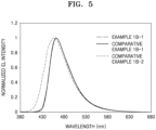
- the organic light-emitting devices of the Examples have color coordinates similar to those of the organic light-emitting devices of the Comparative Examples, but have remarkably improved or similar external quantum efficiency and lifespan, as compared with those of the organic light-emitting devices of the Comparative Examples.
- the organic light-emitting devices of the Examples may have remarkably shorter wavelengths while having a lifespan similar to that of the organic light-emitting devices of the Comparative Examples.
- the organic light-emitting device may have high efficiency and a long lifespan at the same time.
Landscapes
- Physics & Mathematics (AREA)
- Chemical & Material Sciences (AREA)
- Optics & Photonics (AREA)
- Engineering & Computer Science (AREA)
- Materials Engineering (AREA)
- Spectroscopy & Molecular Physics (AREA)
- Crystallography & Structural Chemistry (AREA)
- Inorganic Chemistry (AREA)
- Electroluminescent Light Sources (AREA)
Claims (13)
- Organische lichtemittierende Vorrichtung, umfassend:eine erste Elektrode (11, 110, 210);eine zweite Elektrode (19, 190, 290), die der ersten Elektrode zugewandt ist; undeine organische Schicht (15), die zwischen der ersten Elektrode und der zweiten Elektrode angeordnet ist,wobeidie organische Schicht eine Emissionsschicht (151, 152, 251, 252) umfasst,die Emissionsschicht eine erste Verbindung, eine zweite Verbindung und eine dritte Verbindung umfasst und sich die erste Verbindung und die zweite Verbindung voneinander unterscheiden,wobei jede von der ersten Verbindung und der zweiten Verbindung Licht emittiert,wobei die dritte Verbindung kein Licht emittiert,wobei die erste Verbindung und die zweite Verbindung eine der Bedingungen 1 bis 4 erfüllen:wobei Bedingung 1 Folgendes umfasst:400 Nanometer ≤ λmax1 < 500 Nanometer und400 Nanometer ≤ λmax2 < 500 Nanometer,wobei Bedingung 2 Folgendes umfasst:500 Nanometer ≤ λmax1 < 550 Nanometer und500 Nanometer ≤ λmax2 < 550 Nanometer,wobei Bedingung 3 Folgendes umfasst:550 Nanometer ≤ λmax1 < 620 Nanometer und550 Nanometer ≤ λmax2 < 620 Nanometer oderwobei Bedingung 4 Folgendes umfasst:620 Nanometer ≤ λmax1 < 700 Nanometer und620 Nanometer ≤ λmax2 < 700 Nanometer,die erste Verbindung und die zweite Verbindung die Ungleichung (1-1) erfüllen:
 die erste Verbindung und die zweite Verbindung die Ungleichung (2) erfüllen:
 wobei in den Bedingungen 1 bis 4 und Ungleichungen 1-1 und 2,λmax1 eine maximale Emissionswellenlänge der ersten Verbindung ist,λmax2 eine maximale Emissionswellenlänge der zweiten Verbindung ist,PLS(C1) eine Photostabilität der ersten Verbindung ist,PLS(C2) eine Photostabilität der zweiten Verbindung ist,kr(C1) eine Strahlungszerfallrate der ersten Verbindung ist undkr(C2) eine Strahlungszerfallrate der zweiten Verbindung ist,wobei PLS(C1) durch Gleichung P berechnet wird:
 wobei in Gleichung P I1(C1) die maximale Lichtintensität ist, die durch Messen von PL-Spektren bei Raumtemperatur in einer inerten Umgebung erhalten wird, in der Außenluft abgeblockt wird, unmittelbar nachdem ein Film durch Abscheiden einer Verbindung gebildet wurde, und I2(C1) die maximale Lichtintensität ist, die durch Messen von PL-Spektren bei Raumtemperatur in einer inerten Umgebung erhalten wird, in der Außenluft abgeblockt wird, in Bezug auf einen Film, nach Aussetzen gegenüber Pumplaserlicht für 3 Stunden, das zur Bewertung von I1(C1) in einer inerten Umgebung verwendet wird, in der Außenluft abgeblockt wird,wobei PLS(C2) in gleicher Weise in Bezug auf die zweite Verbindung berechnet wird,wobei λmax1 sich auf einen Wellenlängenwert der ersten Verbindung bezieht, die auf eine Konzentration von 10 mM in CHCl3 verdünnt ist, was die größte Intensität in einem Photolumineszenz(PL)-Spektrum angibt, das bei Raumtemperatur unter Verwendung eines Spektrofluorometers erhalten wird, das mit einer Xenonlampe ausgestattet ist,wobei λmax2 an der zweiten Verbindung unter der gleichen Bedingung gemessen wird,wobei der Wert von kr(C1) durch Photolumineszenz-Quanteneffizienz (PLQY) und Zerfallslebensdauer (Tau) gemessen in einem Dünnfilm berechnet wird, der durch Mischen der ersten Verbindung mit Polymethyl(meth)acrylat (PMMA) oder der dritten Verbindung hergestellt wird, undder Wert von kr(C2) in gleicher Weise wie kr(C1) gemessen wird, mit der Ausnahme, dass die erste Verbindung in die zweite Verbindung geändert wird.
 - Organische lichtemittierende Vorrichtung nach Anspruch 1, wobeieine Menge der ersten Verbindung in der Emissionsschicht größer als eine Menge der zweiten Verbindung in der Emissionsschicht ist; und/oderwobeieine Menge der ersten Verbindung und eine Menge der zweiten Verbindung in der Emissionsschicht jeweils unabhängig in einem Bereich von 1 Gewichtsprozent bis 20 Gewichtsprozent basierend auf dem Gesamtgewicht der Emissionsschicht liegen.
- Organische lichtemittierende Vorrichtung nach Anspruch 1 oder 2, wobeidie erste Verbindung und die zweite Verbindung jeweils unabhängig eine Photolumineszenz-Quantenausbeute (PLQY) von 10 % bis 100 % aufweisen; und/oderwobeieine Bandlücke (Eg1) der ersten Verbindung und eine Bandlücke (Eg2) der zweiten Verbindung die Ungleichung (2-4) erfüllen:
 wobei die Bandlücke (Eg1) und die Bandlücke (Eg2) in Elektronenvolt ausgedrückt werden.
 - Organische lichtemittierende Vorrichtung nach einem der Ansprüche 1-3, wobeidie erste Verbindung und die zweite Verbindung jeweils ein verzögerter Fluoreszenzemitter sind;die erste Verbindung und die zweite Verbindung jeweils ein Phosphoreszenzemitter sind;die erste Verbindung ein verzögerter Fluoreszenzemitter ist und die zweite Verbindung ein Phosphoreszenzemitter ist;die erste Verbindung ein Phosphoreszenzemitter ist und die zweite Verbindung ein verzögerter Fluoreszenzemitter ist; oderdie erste Verbindung und die zweite Verbindung jeweils ein Fluoreszenzemitter sind.
- Organische lichtemittierende Vorrichtung nach Anspruch 4, wobeider verzögerte Fluoreszenzemitter die Ungleichung (3) erfüllt:
 wobei in Ungleichung 3ES1(TADF) ein niedrigstes Singulett-Anregungsenergieniveau des verzögerten Fluoreszenzemitters in Elektronenvolt ist, undET1(TADF) ein niedrigstes Triplett-Anregungsenergieniveau des verzögerten Fluoreszenzemitters in Elektronenvolt ist; und/oderwobeider verzögerte Fluoreszenzemitter dargestellt ist durch eine der Formeln 1 oder 2:


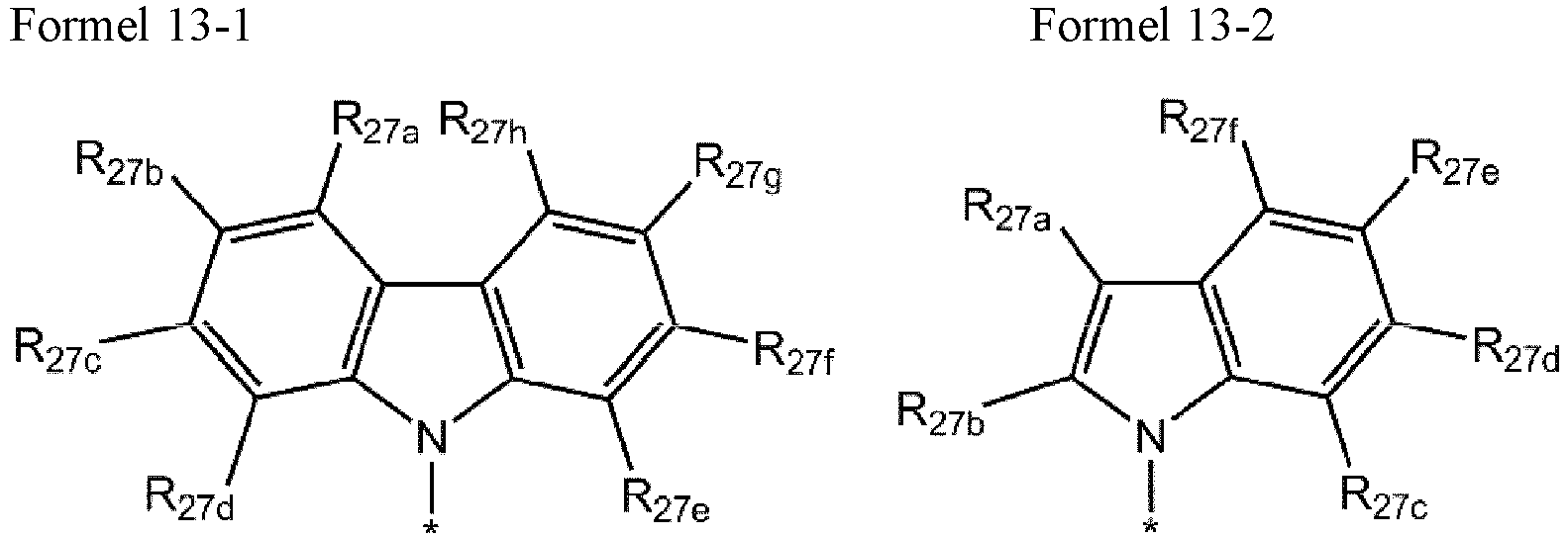 wobei in den Formeln 1, 2, 11-1, 12-1, 13-1 und 13-2D1 eine Gruppe dargestellt durch Formel 11-1 ist,A1 eine Gruppe dargestellt durch Formel 12-1 ist,X11 eine Einfachbindung, O, S, N(R17) oder C(R17)(R18) ist,A11 und A12 jeweils unabhängig eine Benzolgruppe, eine Fluorengruppe, eine Carbazolgruppe, eine Dibenzofurangruppe oder eine Dibenzothiophengruppe sind,L11 und L12 jeweils unabhängig eine substituierte oder unsubstituierte carbocyclische C5-C30-Gruppe oder eine substituierte oder unsubstituierte heterocyclische C1-C30-Gruppe sind,a11 und a12 jeweils unabhängig 0, 1, 2 oder 3 sind,X11a N oder C(R11a) ist; X11b N oder C(R11b) ist; X11c N oder C(R11c) ist; X11d N oder C(R11d) ist; und X11e N oder C(R11e) ist, wobei mindestens eines von X11a bis X11e N ist,R21 bis R26 jeweils unabhängig eine Gruppe dargestellt durch Formel 13-1, eine Gruppe dargestellt durch Formel 13-2, Wasserstoff, Deuterium, -F, -Cl, -Br, -I, eine Hydroxylgruppe, eine Cyanogruppe, eine substituierte oder unsubstituierte C1-C60-Alkylgruppe, eine substituierte oder unsubstituierte C1-C60-Alkoxygruppe, eine substituierte oder unsubstituierte C6-C60-Arylgruppe, eine substituierte oder unsubstituierte C6-C60-Aryloxygruppe, eine substituierte oder unsubstituierte C6-C60-Arylthiogruppe oder eine substituierte oder unsubstituierte C1-C6o-Heteroarylgruppe sind,mindestens eines von R21 bis R26 eine Cyanogruppe ist,mindestens eines von R21 bis R26 eine durch Formel 13-1 dargestellte Gruppe und eine durch Formel 13-2 dargestellte Gruppe ist,R11 bis R18, R11a bis R11e und R27a bis R27h jeweils unabhängig Wasserstoff, Deuterium, -F, -Cl, -Br, -I, eine Hydroxylgruppe, eine Cyanogruppe, eine Nitrogruppe, eine Aminogruppe, eine Amidinogruppe, eine Hydrazingruppe, eine Hydrazongruppe, eine Carbonsäuregruppe oder ein Salz davon, eine Sulfonsäuregruppe oder ein Salz davon, eine Phosphorsäuregruppe oder ein Salz davon, eine substituierte oder unsubstituierte C1-C60-Alkylgruppe, eine substituierte oder unsubstituierte C2-C60-Alkenylgruppe, eine substituierte oder unsubstituierte C2-C60-Alkinylgruppe, eine substituierte oder unsubstituierte C1-C60-Alkoxygruppe, eine substituierte oder unsubstituierte C3-C10-Cycloalkylgruppe, eine substituierte oder unsubstituierte C1-C10-Heterocycloalkylgruppe, eine substituierte oder unsubstituierte C3-C10-Cycloalkenylgruppe, eine substituierte oder unsubstituierte C1-C10-Heterocycloalkenylgruppe, eine substituierte oder unsubstituierte C6-C60-Arylgruppe, eine substituierte oder unsubstituierte C6-C60-Aryloxygruppe, eine substituierte oder unsubstituierte C6-C60-Arylthiogruppe, eine substituierte oder unsubstituierte C1-C60-Heteroarylgruppe, eine substituierte oder unsubstituierte monovalente nichtaromatische kondensierte polycyclische Gruppe, eine substituierte oder unsubstituierte monovalente nichtaromatische kondensierte heteropolycyclische Gruppe, -Si(Q1)(Q2)(Q3), - N(Q4)(Q5) oder -B(Q6)(Q7) sind,b15 und b16 jeweils unabhängig 1, 2, 3, 4, 5, 6, 7 oder 8 sind,Q1 bis Q7 jeweils unabhängig Wasserstoff, eine C1-C60-Alkylgruppe, eine C2-C60-Alkenylgruppe, eine C2-C60-Alkinylgruppe, eine C1-C60-Alkoxygruppe, eine C3-C10-Cycloalkylgruppe, eine C1-C10-Heterocycloalkylgruppe, eine C3-C10-Cycloalkenylgruppe, eine C1-C10-Heterocycloalkenylgruppe, eine C6-C60-Arylgruppe, eine C1-C60-Heteroarylgruppe, eine monovalente nichtaromatische kondensierte polycyclische Gruppe oder eine monovalente nichtaromatische kondensierte heteropolycyclische Gruppe sind und* eine Bindungsstelle zu einem benachbarten Atom angibt.
 - Organische lichtemittierende Vorrichtung nach Anspruch 4 oder 5, wobeider Phosphoreszenzemitter durch Formel 81 dargestellt ist:

 wobei in den Formeln 81 und 81AM ein Übergangsmetall der ersten Zeile, ein Übergangsmetall der zweiten Zeile oder ein Übergangsmetall der dritten Zeile des Periodensystems der Elemente ist,L81 ein Ligand ist, der durch Formel 81A dargestellt wird, und n81 eine ganze Zahl von 1 bis 3 ist, wobei, wenn n81 zwei oder mehr ist, zwei oder mehr Gruppen L81 identisch miteinander oder unterschiedlich voneinander sind,L82 ein organischer Ligand ist und n82 eine ganze Zahl von 0 bis 4 ist, wobei, wenn n82 zwei oder mehr ist, zwei oder mehr Gruppen L82 miteinander identisch oder voneinander verschieden sind,Y81 bis Y84 jeweils unabhängig Kohlenstoff (C) oder Stickstoff (N) sind,Y81 und Y82 über eine Einzelbindung oder eine Doppelbindung verbunden sind und Y83 und Y84 über eine Einzelbindung oder eine Doppelbindung verbunden sind,CY81 und CY82 jeweils unabhängig eine carbocyclische C5-C30-Gruppe oder eine heterocarbocyclische C3-C30-Gruppe sind,CY81 und CY82 optional über eine organische Verbindungsgruppe verbunden sind,R81 und R82 jeweils unabhängig Wasserstoff, Deuterium, -F, -Cl, -Br, -I, eine Hydroxylgruppe, eine Cyanogruppe, eine Nitrogruppe, eine Aminogruppe, eine Amidinogruppe, eine Hydrazingruppe, eine Hydrazongruppe, eine Carbonsäuregruppe oder ein Salz davon, eine Sulfonsäuregruppe oder ein Salz davon, eine Phosphorsäuregruppe oder ein Salz davon, -SF5, eine substituierte oder unsubstituierte C1-C60-Alkylgruppe, eine substituierte oder unsubstituierte C2-C60-Alkenylgruppe, eine substituierte oder unsubstituierte C2-C60-Alkinylgruppe, eine substituierte oder unsubstituierte C1-C60-Alkoxygruppe, eine substituierte oder unsubstituierte C3-C10-Cycloalkylgruppe, eine substituierte oder unsubstituierte C1-C10-Heterocycloalkylgruppe, eine substituierte oder unsubstituierte C3-C10-Cycloalkenylgruppe, eine substituierte oder unsubstituierte C1-C10-Heterocycloalkenylgruppe, eine substituierte oder unsubstituierte C6-C60-Arylgruppe, eine substituierte oder unsubstituierte C6-C60-Aryloxygruppe, eine substituierte oder unsubstituierte C6-C60-Arylthiogruppe, eine substituierte oder unsubstituierte C1-C60-Heteroarylgruppe, eine substituierte oder unsubstituierte monovalente nichtaromatische kondensierte polycyclische Gruppe, eine substituierte oder unsubstituierte monovalente nichtaromatische kondensierte heteropolycyclische Gruppe, -Si(Q81)(Q82)(Q83), -N(Q84)(Q85), - B(Q86)(Q87) oder -P(=O)(Q88)(Q89) sind,a81 und a82 jeweils unabhängig eine ganze Zahl von 1 bis 5 sind,wobei, wenn a81 zwei oder mehr ist, zwei oder mehr Gruppen R81 miteinander identisch oder voneinander verschieden sind,wobei, wenn a82 zwei oder mehr ist, zwei oder mehr Gruppen R82 miteinander identisch oder voneinander verschieden sind,wobei, wenn a81 zwei oder mehr ist, benachbarte Gruppen R81 optional verbunden sind, um einen gesättigten oder ungesättigten Ring zu bilden,wobei, wenn a82 zwei oder mehr ist, benachbarte Gruppen R82 optional verbunden sind, um einen gesättigten oder ungesättigten Ring zu bilden,zwei, drei oder vier ausgewählt aus einer Vielzahl von benachbarten R81(s)und R82(s) optional verbunden sind, um einen vierfach koordinierten, sechsfach koordinierten oder achtfach koordinierten Liganden zu bilden,* und *' in Formel 81A jeweils eine Bindungsstelle zu M in Formel 81 angeben, undQ81 bis Q89 und Q91 bis Q93 jeweils unabhängig Wasserstoff, Deuterium, eine C1-C60-Alkylgruppe, eine C1-C60-Alkoxygruppe, eine C3-C10-Cycloalkylgruppe, eine C1-C10-Heterocycloalkylgruppe, eine C3-C10-Cycloalkenylgruppe, eine C1-C10-Heterocycloalkenylgruppe, eine C6-C60-Arylgruppe, eine C1-C60-Heteroarylgruppe, eine monovalente nichtaromatische kondensierte polycyclische Gruppe oder eine monovalente nichtaromatische kondensierte heteropolycyclische Gruppe sind.
 - Organische lichtemittierende Vorrichtung nach einem der Ansprüche 4-6, wobei der Fluoreszenzemitter die Ungleichung 4 erfüllt:
 ES1(F) ein niedrigstes Singulett-Anregungsenergieniveau des Fluoreszenzemitters ist, undET1(F) ein niedrigstes Triplett-Anregungsenergieniveau des Fluoreszenzemitters ist.
 - Organische lichtemittierende Vorrichtung nach einem der Ansprüche 1-7, wobei die dritte Verbindung mindestens eine von Ungleichungen (7-1) bis (7-4) erfüllt:



 S1(C1) ein niedrigstes Singulett-Anregungsenergieniveau der ersten Verbindung ist,T1(C1) ein niedrigstes Triplett-Anregungsenergieniveau der ersten Verbindung ist,S1(C2) ein niedrigstes Singulett-Anregungsenergieniveau der zweiten Verbindung ist,T1(C2) ein niedrigstes Triplett-Anregungsenergieniveau der zweiten Verbindung ist,S1(C3) ein niedrigstes Singulett-Anregungsenergieniveau der dritten Verbindung ist, undT1(C3) ein niedrigstes Triplett-Anregungsenergieniveau der dritten Verbindung ist;wobei bevorzugtdie erste Verbindung und die zweite Verbindung jeweils ein verzögerter Fluoreszenzemitter sind und die erste Verbindung und die zweite Verbindung die Ungleichungen (7-1) bis (7-4) erfüllen; oderdie erste Verbindung und die zweite Verbindung jeweils ein Phosphoreszenzemitter sind und die erste Verbindung und die zweite Verbindung die Ungleichungen (7-2) und (7-4) erfüllen; oderdie erste Verbindung ein verzögerter Fluoreszenzemitter ist, die zweite Verbindung ein Phosphoreszenzemitter ist und die erste Verbindung und die zweite Verbindung die Ungleichungen (7-1), (7-2) und (7-4) erfüllen; oderdie erste Verbindung ein Phosphoreszenzemitter ist, die zweite Verbindung ein verzögerter Fluoreszenzemitter ist und die erste Verbindung und die zweite Verbindung die Ungleichungen )7-2) bis (7-4) erfüllen; oderdie erste Verbindung und die zweite Verbindung jeweils ein Fluoreszenzemitter sind und die erste Verbindung und die zweite Verbindung die Ungleichungen (7-1) und )7-3) erfüllen.
 - Organische lichtemittierende Vorrichtung nach einem der Ansprüche 1-8, wobeidie dritte Verbindung einen Elektronentransportwirt, einen Lochtransportwirt oder eine Kombination davon umfasst,der Elektronentransportwirt eine Elektronentransportkomponente umfasst, undder Lochtransportwirt keine Elektronentransportkomponente umfasst.
- Organische lichtemittierende Vorrichtung nach Anspruch 9, wobeider Elektronentransportwirt eine Verbindung umfasst, die durch eine der Formeln 3-1 oder 3-2 dargestellt ist:

 wobei in den Formeln 3-1, 3-2 und 13-1 bis 13-3Y31 eine Gruppe ist, die durch eine der Formeln 13-1 bis 13-3 dargestellt ist,A31 bis A36 jeweils unabhängig eine Benzolgruppe, eine Naphthalengruppe, eine Fluorengruppe, eine Carbazolgruppe, eine Dibenzosilolgruppe, eine Dibenzofurangruppe oder eine Dibenzothiophengruppe sind,X31 und X32 jeweils unabhängig O oder S sind,m 0, 1 oder 2 ist,n 1 oder 2 ist,R31 bis R37 jeweils unabhängig Wasserstoff, Deuterium, -F, -Cl, -Br, -I, eine Hydroxylgruppe, eine Cyanogruppe, eine Nitrogruppe, eine Aminogruppe, eine Amidinogruppe, eine Hydrazingruppe, eine Hydrazongruppe, eine Carbonsäuregruppe oder ein Salz davon, eine Sulfonsäuregruppe oder ein Salz davon, eine Phosphorsäuregruppe oder ein Salz davon, eine substituierte oder unsubstituierte C1-C60-Alkylgruppe, eine substituierte oder unsubstituierte C2-C60-Alkenylgruppe, eine substituierte oder unsubstituierte C2-C60-Alkinylgruppe, eine substituierte oder unsubstituierte C1-C60-Alkoxygruppe, eine substituierte oder unsubstituierte C3-C10-Cycloalkylgruppe, eine substituierte oder unsubstituierte C1-C10-Heterocycloalkylgruppe, eine substituierte oder unsubstituierte C3-C10-Cycloalkenylgruppe, eine substituierte oder unsubstituierte C1-C10-Heterocycloalkenylgruppe, eine substituierte oder unsubstituierte C6-C60-Arylgruppe, eine substituierte oder unsubstituierte C6-C60-Aryloxygruppe, eine substituierte oder unsubstituierte C6-C60-Arylthiogruppe, eine substituierte oder unsubstituierte C1-C60-Heteroarylgruppe, eine substituierte oder unsubstituierte monovalente nichtaromatische kondensierte polycyclische Gruppe, eine substituierte oder unsubstituierte monovalente nichtaromatische kondensierte heteropolycyclische Gruppe, -Si(Q1)(Q2)(Q3), -N(Q1)(Q2) oder - B(Q1)(Q2) sind,b31 bis b34, b36 und b37 jeweils unabhängig 1, 2, 3 oder 4 sind,* eine Bindungsstelle zu einem benachbarten Atom angibt unddie Verbindung, die durch eine der Formeln 3-1 oder 3-2 dargestellt ist, eine Cyanogruppe umfasst.
 - Organische lichtemittierende Vorrichtung nach Anspruch 9 oder 10, wobeider Lochtransportwirt eine Verbindung umfasst, die durch eine der Formeln 4-1 bis 4-3 dargestellt ist:

 wobei in Formel 4-1 bis 4-3A41 bis A44 jeweils unabhängig eine Benzolgruppe, eine Naphthalengruppe, eine Indengruppe, eine Benzofurangruppe, eine Benzothiophengruppe, eine Benzosilolgruppe, eine Fluorengruppe, eine Carbazolgruppe, eine Dibenzofurangruppe, eine Dibenzothiophengruppe oder eine Dibenzosilolgruppe sind,X41 und X42 jeweils unabhängig eine Einfachbindung, O, S, N(R45) oder C(R45)(R46) sind,X43 und X44 jeweils unabhängig O, S, N(R47) oder C(R47)(R48) sind,L41 eine an π-Elektronen abgereicherte stickstofffreie cyclische Gruppe, unsubstituiert oder substituiert mit Deuterium, eine C1-C10-Alkylgruppe, eine C1-C10-Alkoxygruppe, einer Phenylgruppe, eine Naphthylgruppe, eine Fluorenylgruppe, eine Carbazolylgruppe, eine Dibenzofuranylgruppe, eine Dibenzothiophenylgruppe, eine Triphenylenylgruppe, eine Biphenylgruppe, eine Terphenylgruppe, eine Tetraphenylgruppe, -Si(Q401)(Q402)(Q403) oder eine Kombination davon ist,a41 0, 1, 2 oder 3 ist,R41 bis R48 jeweils unabhängig Folgendes sind: Wasserstoff, Deuterium, eine C1-C10-Alkylgruppe oder eine C1-C10-Alkoxygruppe, oder eine an π-Elektronen abgereicherte stickstofffreie cyclische Gruppe unsubstituiert oder substituiert mit Deuterium, eine C1-C10-Alkylgruppe, eine C1-C10-Alkoxygruppe, eine Phenylgruppe, eine Naphthylgruppe, eine Fluorenylgruppe, eine Carbazolylgruppe, eine Dibenzofuranylgruppe, eine Dibenzothiophenylgruppe, eine Triphenylenylgruppe, eine Biphenylgruppe, eine Terphenylgruppe, eine Tetraphenylgruppe, -Si(Q401)(Q402)(Q403) oder eine Kombination davon,Q401 bis Q403 jeweils unabhängig Wasserstoff, Deuterium, eine C1-C10-Alkylgruppe, eine C1-C10-Alkoxygruppe, eine Phenylgruppe, eine Naphthylgruppe, eine Fluorenylgruppe, eine Carbazolylgruppe, eine Dibenzofuranylgruppe, eine Dibenzothiophenylgruppe, eine Triphenylenylgruppe, eine Biphenylgruppe, eine Terphenylgruppe oder eine Tetraphenylgruppe sind undb41 und b44 jeweils unabhängig 1, 2, 3, 4, 5, 6, 7 oder 8 sind.
 - Organische lichtemittierende Vorrichtung gemäß einem der Ansprüche 1-11:ferner umfassend eine Vielzahl von lichtemittierenden Einheiten in der Anzahl von m, die zwischen der ersten Elektrode und der zweiten Elektrode angeordnet sind, wobei jede lichtemittierende Einheit eine Emissionsschicht umfasst; undeine Vielzahl von Ladungserzeugungsschichten in der Anzahl von m-1, die zwischen zwei benachbarten lichtemittierenden Einheiten aus der Vielzahl von lichtemittierenden Einheiten angeordnet ist,wobei jede Ladungserzeugungsschicht eine Ladungserzeugungsschicht vom n-Typ und eine Ladungserzeugungsschicht vom p-Typ umfasst,wobeim eine ganze Zahl von 2 oder mehr ist,eine maximale Emissionswellenlänge von Licht, das durch mindestens eine lichtemittierende Einheit aus der Vielzahl von lichtemittierenden Einheiten emittiert wird, sich von einer maximalen Emissionswellenlänge von Licht, das durch mindestens eine andere lichtemittierende Einheit aus der Vielzahl von lichtemittierenden Einheiten emittiert wird, unterscheidet.
- Organische lichtemittierende Vorrichtung nach einem der Ansprüche 1-12, umfassend:eine Vielzahl von Emissionsschichten in der Anzahl von m, die zwischen der ersten Elektrode und der zweiten Elektrode angeordnet ist,wobeim eine ganze Zahl von 2 oder mehr ist,eine maximale Emissionswellenlänge von Licht, das durch mindestens eine Emissionsschicht aus der Vielzahl von Emissionsschichten emittiert wird, sich von einer maximalen Emissionswellenlänge von Licht, das durch mindestens eine andere Emissionsschicht aus der Vielzahl von Emissionsschichten emittiert wird, unterscheidet.
Applications Claiming Priority (2)
| Application Number | Priority Date | Filing Date | Title |
|---|---|---|---|
| KR20180084766 | 2018-07-20 | ||
| KR1020190011305A KR102843325B1 (ko) | 2018-07-20 | 2019-01-29 | 유기 발광 소자 |
Publications (2)
| Publication Number | Publication Date |
|---|---|
| EP3598518A1 EP3598518A1 (de) | 2020-01-22 |
| EP3598518B1 true EP3598518B1 (de) | 2025-05-21 |
Family
ID=66102922
Family Applications (1)
| Application Number | Title | Priority Date | Filing Date |
|---|---|---|---|
| EP19168054.5A Active EP3598518B1 (de) | 2018-07-20 | 2019-04-09 | Organische lichtemittierende vorrichtung |
Country Status (3)
| Country | Link |
|---|---|
| US (1) | US11367837B2 (de) |
| EP (1) | EP3598518B1 (de) |
| CN (1) | CN110739405B (de) |
Families Citing this family (4)
| Publication number | Priority date | Publication date | Assignee | Title |
|---|---|---|---|---|
| CN111372918B (zh) | 2018-07-27 | 2023-09-05 | 出光兴产株式会社 | 化合物、用于有机电致发光元件的材料、有机电致发光元件以及电子设备 |
| KR102675778B1 (ko) * | 2018-09-19 | 2024-06-18 | 삼성전자주식회사 | 유기 발광 소자 |
| KR102934006B1 (ko) * | 2020-12-29 | 2026-03-04 | 엘지디스플레이 주식회사 | 백색 발광 소자 및 이를 포함한 발광 표시 장치 |
| KR102949682B1 (ko) | 2021-07-22 | 2026-04-06 | 삼성전자주식회사 | 형광 화합물을 포함한 발광 소자, 상기 발광 소자를 포함한 전자 장치 및 형광 화합물 |
Family Cites Families (26)
| Publication number | Priority date | Publication date | Assignee | Title |
|---|---|---|---|---|
| DE102009052428A1 (de) * | 2009-11-10 | 2011-05-12 | Merck Patent Gmbh | Verbindung für elektronische Vorrichtungen |
| JP2012151322A (ja) | 2011-01-20 | 2012-08-09 | Konica Minolta Holdings Inc | 白色発光有機エレクトロルミネッセンス素子及び照明装置 |
| US9190623B2 (en) | 2012-11-20 | 2015-11-17 | Universal Display Corporation | Organic electroluminescent materials and devices |
| JP6215842B2 (ja) | 2012-12-28 | 2017-10-18 | 出光興産株式会社 | 有機エレクトロルミネッセンス素子 |
| JP5669163B1 (ja) * | 2013-08-14 | 2015-02-12 | 国立大学法人九州大学 | 有機エレクトロルミネッセンス素子 |
| EP3117470B1 (de) | 2014-03-13 | 2020-12-23 | Merck Patent GmbH | Organische elektrolumineszenzvorrichtung |
| KR102326623B1 (ko) | 2014-03-18 | 2021-11-16 | 메르크 파텐트 게엠베하 | 유기 전계발광 소자 |
| CN106488917B (zh) * | 2014-06-18 | 2020-05-05 | 默克专利有限公司 | 用于有机电致发光器件的材料 |
| CN106328816B (zh) * | 2015-06-16 | 2018-11-13 | 昆山国显光电有限公司 | 一种有机电致发光器件及其制备方法 |
| US10062852B2 (en) | 2015-06-23 | 2018-08-28 | Samsung Electronics Co., Ltd. | Condensed cyclic compound and organic light-emitting device including the same |
| KR102587060B1 (ko) | 2015-06-23 | 2023-10-11 | 삼성전자주식회사 | 축합환 화합물 및 이를 포함한 유기 발광 소자 |
| US10240085B2 (en) | 2015-08-27 | 2019-03-26 | Samsung Electronics Co., Ltd. | Thin film and organic light-emitting device including the same |
| KR102460657B1 (ko) | 2015-08-31 | 2022-10-28 | 삼성전자주식회사 | 유기 발광 소자 |
| US10297764B2 (en) * | 2015-09-14 | 2019-05-21 | Samsung Electronics Co., Ltd. | Mixture, thin film, and organic light emitting device including mixture and thin film |
| KR102520026B1 (ko) * | 2015-12-30 | 2023-04-07 | 엘지디스플레이 주식회사 | 유기 발광 소자 |
| KR102642199B1 (ko) * | 2016-04-07 | 2024-03-05 | 삼성디스플레이 주식회사 | 유기 발광 소자 |
| TWI631116B (zh) * | 2016-05-09 | 2018-08-01 | 國立臺灣大學 | 螺環吖啶三嗪化合物及電致發光裝置的應用 |
| KR102727643B1 (ko) * | 2016-12-07 | 2024-11-08 | 삼성디스플레이 주식회사 | 축합환 화합물 및 이를 포함한 유기 발광 소자 |
| KR102532601B1 (ko) * | 2016-12-14 | 2023-05-16 | 삼성전자주식회사 | 유기 발광 소자 및 화합물 |
| KR102852285B1 (ko) * | 2017-02-27 | 2025-08-28 | 삼성전자주식회사 | 축합환 화합물 및 이를 포함한 유기 발광 소자 |
| CN106653821B (zh) * | 2017-03-09 | 2019-10-25 | 上海天马有机发光显示技术有限公司 | 一种oled显示面板和包含其的显示装置 |
| US20180277766A1 (en) * | 2017-03-27 | 2018-09-27 | The Regents Of The University Of California | Thermally activated delayed fluorescence organic light emitting diode having host matrix polarity co-doping |
| EP3490023B1 (de) | 2017-11-22 | 2020-04-22 | Samsung Electronics Co., Ltd. | Zusammensetzung, dünnschicht mit der zusammensetzung und organische lichtemittierende vorrichtung mit der dünnschicht |
| US20190181353A1 (en) | 2017-12-07 | 2019-06-13 | Samsung Electronics Co., Ltd. | Organic light-emitting device |
| JPWO2019186717A1 (ja) * | 2018-03-27 | 2021-03-18 | シャープ株式会社 | 発光装置および表示装置 |
| US11063224B2 (en) * | 2018-05-30 | 2021-07-13 | Kunshan Go-Visionox Opto-Electronics Co., Ltd. | Organic electroluminescent device |
-
2019
- 2019-04-04 US US16/375,333 patent/US11367837B2/en active Active
- 2019-04-09 EP EP19168054.5A patent/EP3598518B1/de active Active
- 2019-06-27 CN CN201910565770.3A patent/CN110739405B/zh active Active
Also Published As
| Publication number | Publication date |
|---|---|
| CN110739405B (zh) | 2024-07-26 |
| EP3598518A1 (de) | 2020-01-22 |
| US11367837B2 (en) | 2022-06-21 |
| CN110739405A (zh) | 2020-01-31 |
| US20200028094A1 (en) | 2020-01-23 |
Similar Documents
| Publication | Publication Date | Title |
|---|---|---|
| EP3739645B1 (de) | Organische lichtemittierende vorrichtung | |
| EP3617202B1 (de) | Heterocyclische verbindung und organische lichtemittierende vorrichtung | |
| EP3367456B1 (de) | Organische lichtemittierende vorrichtung | |
| EP3514163B1 (de) | Organometallische verbindung, organische lichtemittierende vorrichtung damit und diagnosezusammensetzung mit der organometallischen verbindung | |
| KR102725204B1 (ko) | 유기 발광 소자 | |
| EP3439063B1 (de) | Organische lichtemittierende vorrichtung | |
| EP3190164B1 (de) | Zusammensetzung, dünnschicht mit der zusammensetzung und organische lichtemittierende vorrichtung mit der zusammensetzung oder der dünnschicht | |
| EP3142162B1 (de) | Zusammensetzung, dünnschicht und organische lichtemittierende vorrichtung mit der zusammensetzung und der dünnschicht | |
| EP3211681B1 (de) | Organische lichtemittierende vorrichtung | |
| CN103858249B (zh) | 有机电致发光器件 | |
| EP3604321B1 (de) | Organometallische verbindung, organische lichtemittierende vorrichtung damit und diagnosezusammensetzung mit der organometallischen verbindung | |
| CN107043346A (zh) | 组合物、薄膜、以及包括组合物和薄膜的有机发光器件 | |
| EP3392258B1 (de) | Organometallische verbindung, organische lichtemittierende vorrichtung mit der organometallischen verbindung und diagnostische zusammensetzung mit der organometallischen verbindung | |
| CN102365769A (zh) | 有机电致发光器件 | |
| EP3588602B1 (de) | Organische lichtemittierende vorrichtung | |
| EP3772517B1 (de) | Organometallische verbindung, organische lichtemittierende vorrichtung damit und diagnosezusammensetzung damit | |
| EP3598518A1 (de) | Organische lichtemittierende vorrichtung | |
| EP3395823B1 (de) | Organometallische verbindung, organische lichtemittierende vorrichtung damit und diagnosezusammensetzung mit der organometallischen verbindung | |
| EP3787056B1 (de) | Organische lichtemittierende vorrichtung | |
| KR20190067694A (ko) | 유기 발광 소자 | |
| KR102688060B1 (ko) | 유기금속 화합물 및 이를 포함한 유기 발광 소자 | |
| JP2012532900A (ja) | 電子素子のための材料 | |
| EP3967699A1 (de) | Polycyclische verbindung und organische lichtemittierende vorrichtung damit | |
| EP4395500A1 (de) | Lichtemittierende vorrichtung und elektronische vorrichtung damit | |
| KR102843325B1 (ko) | 유기 발광 소자 |
Legal Events
| Date | Code | Title | Description |
|---|---|---|---|
| PUAI | Public reference made under article 153(3) epc to a published international application that has entered the european phase |
Free format text: ORIGINAL CODE: 0009012 |
|
| STAA | Information on the status of an ep patent application or granted ep patent |
Free format text: STATUS: THE APPLICATION HAS BEEN PUBLISHED |
|
| AK | Designated contracting states |
Kind code of ref document: A1 Designated state(s): AL AT BE BG CH CY CZ DE DK EE ES FI FR GB GR HR HU IE IS IT LI LT LU LV MC MK MT NL NO PL PT RO RS SE SI SK SM TR |
|
| AX | Request for extension of the european patent |
Extension state: BA ME |
|
| STAA | Information on the status of an ep patent application or granted ep patent |
Free format text: STATUS: REQUEST FOR EXAMINATION WAS MADE |
|
| 17P | Request for examination filed |
Effective date: 20200722 |
|
| RBV | Designated contracting states (corrected) |
Designated state(s): AL AT BE BG CH CY CZ DE DK EE ES FI FR GB GR HR HU IE IS IT LI LT LU LV MC MK MT NL NO PL PT RO RS SE SI SK SM TR |
|
| STAA | Information on the status of an ep patent application or granted ep patent |
Free format text: STATUS: EXAMINATION IS IN PROGRESS |
|
| 17Q | First examination report despatched |
Effective date: 20220104 |
|
| P01 | Opt-out of the competence of the unified patent court (upc) registered |
Effective date: 20230520 |
|
| REG | Reference to a national code |
Ref country code: DE Free format text: PREVIOUS MAIN CLASS: H01L0051500000 Ipc: H10K0050110000 Ref country code: DE Ref legal event code: R079 Ref document number: 602019070162 Country of ref document: DE Free format text: PREVIOUS MAIN CLASS: H01L0051500000 Ipc: H10K0050110000 |
|
| GRAP | Despatch of communication of intention to grant a patent |
Free format text: ORIGINAL CODE: EPIDOSNIGR1 |
|
| STAA | Information on the status of an ep patent application or granted ep patent |
Free format text: STATUS: GRANT OF PATENT IS INTENDED |
|
| RIC1 | Information provided on ipc code assigned before grant |
Ipc: H10K 50/11 20230101AFI20250228BHEP |
|
| GRAS | Grant fee paid |
Free format text: ORIGINAL CODE: EPIDOSNIGR3 |
|
| INTG | Intention to grant announced |
Effective date: 20250313 |
|
| RIN1 | Information on inventor provided before grant (corrected) |
Inventor name: CHUNG, YEONSOOK Inventor name: JEON, SOONOK Inventor name: LEE, HASUP Inventor name: KIM, JONGSOO Inventor name: KOISHIKAWA, YASUSHI Inventor name: KIM, JOONGHYUK Inventor name: IHN, SOOGHANG Inventor name: SIM, MYUNGSUN |
|
| GRAA | (expected) grant |
Free format text: ORIGINAL CODE: 0009210 |
|
| STAA | Information on the status of an ep patent application or granted ep patent |
Free format text: STATUS: THE PATENT HAS BEEN GRANTED |
|
| AK | Designated contracting states |
Kind code of ref document: B1 Designated state(s): AL AT BE BG CH CY CZ DE DK EE ES FI FR GB GR HR HU IE IS IT LI LT LU LV MC MK MT NL NO PL PT RO RS SE SI SK SM TR |
|
| REG | Reference to a national code |
Ref country code: GB Ref legal event code: FG4D |
|
| REG | Reference to a national code |
Ref country code: CH Ref legal event code: EP |
|
| REG | Reference to a national code |
Ref country code: DE Ref legal event code: R096 Ref document number: 602019070162 Country of ref document: DE |
|
| REG | Reference to a national code |
Ref country code: IE Ref legal event code: FG4D |
|
| REG | Reference to a national code |
Ref country code: NL Ref legal event code: MP Effective date: 20250521 |
|
| PG25 | Lapsed in a contracting state [announced via postgrant information from national office to epo] |
Ref country code: PT Free format text: LAPSE BECAUSE OF FAILURE TO SUBMIT A TRANSLATION OF THE DESCRIPTION OR TO PAY THE FEE WITHIN THE PRESCRIBED TIME-LIMIT Effective date: 20250922 Ref country code: FI Free format text: LAPSE BECAUSE OF FAILURE TO SUBMIT A TRANSLATION OF THE DESCRIPTION OR TO PAY THE FEE WITHIN THE PRESCRIBED TIME-LIMIT Effective date: 20250521 Ref country code: ES Free format text: LAPSE BECAUSE OF FAILURE TO SUBMIT A TRANSLATION OF THE DESCRIPTION OR TO PAY THE FEE WITHIN THE PRESCRIBED TIME-LIMIT Effective date: 20250521 |
|
| REG | Reference to a national code |
Ref country code: LT Ref legal event code: MG9D |
|
| PG25 | Lapsed in a contracting state [announced via postgrant information from national office to epo] |
Ref country code: NO Free format text: LAPSE BECAUSE OF FAILURE TO SUBMIT A TRANSLATION OF THE DESCRIPTION OR TO PAY THE FEE WITHIN THE PRESCRIBED TIME-LIMIT Effective date: 20250821 Ref country code: GR Free format text: LAPSE BECAUSE OF FAILURE TO SUBMIT A TRANSLATION OF THE DESCRIPTION OR TO PAY THE FEE WITHIN THE PRESCRIBED TIME-LIMIT Effective date: 20250822 |
|
| PG25 | Lapsed in a contracting state [announced via postgrant information from national office to epo] |
Ref country code: PL Free format text: LAPSE BECAUSE OF FAILURE TO SUBMIT A TRANSLATION OF THE DESCRIPTION OR TO PAY THE FEE WITHIN THE PRESCRIBED TIME-LIMIT Effective date: 20250521 Ref country code: NL Free format text: LAPSE BECAUSE OF FAILURE TO SUBMIT A TRANSLATION OF THE DESCRIPTION OR TO PAY THE FEE WITHIN THE PRESCRIBED TIME-LIMIT Effective date: 20250521 |
|
| PG25 | Lapsed in a contracting state [announced via postgrant information from national office to epo] |
Ref country code: BG Free format text: LAPSE BECAUSE OF FAILURE TO SUBMIT A TRANSLATION OF THE DESCRIPTION OR TO PAY THE FEE WITHIN THE PRESCRIBED TIME-LIMIT Effective date: 20250521 |
|
| PG25 | Lapsed in a contracting state [announced via postgrant information from national office to epo] |
Ref country code: HR Free format text: LAPSE BECAUSE OF FAILURE TO SUBMIT A TRANSLATION OF THE DESCRIPTION OR TO PAY THE FEE WITHIN THE PRESCRIBED TIME-LIMIT Effective date: 20250521 |
|
| PG25 | Lapsed in a contracting state [announced via postgrant information from national office to epo] |
Ref country code: RS Free format text: LAPSE BECAUSE OF FAILURE TO SUBMIT A TRANSLATION OF THE DESCRIPTION OR TO PAY THE FEE WITHIN THE PRESCRIBED TIME-LIMIT Effective date: 20250821 |
|
| PG25 | Lapsed in a contracting state [announced via postgrant information from national office to epo] |
Ref country code: IS Free format text: LAPSE BECAUSE OF FAILURE TO SUBMIT A TRANSLATION OF THE DESCRIPTION OR TO PAY THE FEE WITHIN THE PRESCRIBED TIME-LIMIT Effective date: 20250921 |
|
| PG25 | Lapsed in a contracting state [announced via postgrant information from national office to epo] |
Ref country code: LV Free format text: LAPSE BECAUSE OF FAILURE TO SUBMIT A TRANSLATION OF THE DESCRIPTION OR TO PAY THE FEE WITHIN THE PRESCRIBED TIME-LIMIT Effective date: 20250521 |
|
| REG | Reference to a national code |
Ref country code: AT Ref legal event code: MK05 Ref document number: 1798053 Country of ref document: AT Kind code of ref document: T Effective date: 20250521 |
|
| PG25 | Lapsed in a contracting state [announced via postgrant information from national office to epo] |
Ref country code: AT Free format text: LAPSE BECAUSE OF FAILURE TO SUBMIT A TRANSLATION OF THE DESCRIPTION OR TO PAY THE FEE WITHIN THE PRESCRIBED TIME-LIMIT Effective date: 20250521 Ref country code: DK Free format text: LAPSE BECAUSE OF FAILURE TO SUBMIT A TRANSLATION OF THE DESCRIPTION OR TO PAY THE FEE WITHIN THE PRESCRIBED TIME-LIMIT Effective date: 20250521 Ref country code: SM Free format text: LAPSE BECAUSE OF FAILURE TO SUBMIT A TRANSLATION OF THE DESCRIPTION OR TO PAY THE FEE WITHIN THE PRESCRIBED TIME-LIMIT Effective date: 20250521 |
|
| PG25 | Lapsed in a contracting state [announced via postgrant information from national office to epo] |
Ref country code: CZ Free format text: LAPSE BECAUSE OF FAILURE TO SUBMIT A TRANSLATION OF THE DESCRIPTION OR TO PAY THE FEE WITHIN THE PRESCRIBED TIME-LIMIT Effective date: 20250521 |
|
| PG25 | Lapsed in a contracting state [announced via postgrant information from national office to epo] |
Ref country code: EE Free format text: LAPSE BECAUSE OF FAILURE TO SUBMIT A TRANSLATION OF THE DESCRIPTION OR TO PAY THE FEE WITHIN THE PRESCRIBED TIME-LIMIT Effective date: 20250521 |
|
| PG25 | Lapsed in a contracting state [announced via postgrant information from national office to epo] |
Ref country code: RO Free format text: LAPSE BECAUSE OF FAILURE TO SUBMIT A TRANSLATION OF THE DESCRIPTION OR TO PAY THE FEE WITHIN THE PRESCRIBED TIME-LIMIT Effective date: 20250521 Ref country code: SK Free format text: LAPSE BECAUSE OF FAILURE TO SUBMIT A TRANSLATION OF THE DESCRIPTION OR TO PAY THE FEE WITHIN THE PRESCRIBED TIME-LIMIT Effective date: 20250521 |
|
| PG25 | Lapsed in a contracting state [announced via postgrant information from national office to epo] |
Ref country code: IT Free format text: LAPSE BECAUSE OF FAILURE TO SUBMIT A TRANSLATION OF THE DESCRIPTION OR TO PAY THE FEE WITHIN THE PRESCRIBED TIME-LIMIT Effective date: 20250521 |
|
| REG | Reference to a national code |
Ref country code: DE Ref legal event code: R097 Ref document number: 602019070162 Country of ref document: DE |
|
| PLBE | No opposition filed within time limit |
Free format text: ORIGINAL CODE: 0009261 |
|
| STAA | Information on the status of an ep patent application or granted ep patent |
Free format text: STATUS: NO OPPOSITION FILED WITHIN TIME LIMIT |
|
| REG | Reference to a national code |
Ref country code: CH Ref legal event code: L10 Free format text: ST27 STATUS EVENT CODE: U-0-0-L10-L00 (AS PROVIDED BY THE NATIONAL OFFICE) Effective date: 20260402 |
|
| PGFP | Annual fee paid to national office [announced via postgrant information from national office to epo] |
Ref country code: GB Payment date: 20260323 Year of fee payment: 8 |
|
| PGFP | Annual fee paid to national office [announced via postgrant information from national office to epo] |
Ref country code: FR Payment date: 20260323 Year of fee payment: 8 |
|
| 26N | No opposition filed |
Effective date: 20260224 |