EP3589091B1 - Dispositif électronique comportant un transistor discret monté sur une carte de circuit imprimé - Google Patents
Dispositif électronique comportant un transistor discret monté sur une carte de circuit imprimé Download PDFInfo
- Publication number
- EP3589091B1 EP3589091B1 EP19181822.8A EP19181822A EP3589091B1 EP 3589091 B1 EP3589091 B1 EP 3589091B1 EP 19181822 A EP19181822 A EP 19181822A EP 3589091 B1 EP3589091 B1 EP 3589091B1
- Authority
- EP
- European Patent Office
- Prior art keywords
- transistor
- printed circuit
- circuit board
- pad
- connection
- Prior art date
- Legal status (The legal status is an assumption and is not a legal conclusion. Google has not performed a legal analysis and makes no representation as to the accuracy of the status listed.)
- Active
Links
Images


Classifications
-
- H—ELECTRICITY
- H05—ELECTRIC TECHNIQUES NOT OTHERWISE PROVIDED FOR
- H05K—PRINTED CIRCUITS; CASINGS OR CONSTRUCTIONAL DETAILS OF ELECTRIC APPARATUS; MANUFACTURE OF ASSEMBLAGES OF ELECTRICAL COMPONENTS
- H05K3/00—Apparatus or processes for manufacturing printed circuits
- H05K3/30—Assembling printed circuits with electric components, e.g. with resistors
- H05K3/32—Assembling printed circuits with electric components, e.g. with resistors electrically connecting electric components or wires to printed circuits
- H05K3/34—Assembling printed circuits with electric components, e.g. with resistors electrically connecting electric components or wires to printed circuits by soldering
- H05K3/341—Surface mounted components
- H05K3/3431—Leadless components
- H05K3/3436—Leadless components having an array of bottom contacts, e.g. pad grid array or ball grid array components
-
- H—ELECTRICITY
- H10—SEMICONDUCTOR DEVICES; ELECTRIC SOLID-STATE DEVICES NOT OTHERWISE PROVIDED FOR
- H10W—GENERIC PACKAGES, INTERCONNECTIONS, CONNECTORS OR OTHER CONSTRUCTIONAL DETAILS OF DEVICES COVERED BY CLASS H10
- H10W90/00—Package configurations
- H10W90/701—Package configurations characterised by the relative positions of pads or connectors relative to package parts
-
- H—ELECTRICITY
- H10—SEMICONDUCTOR DEVICES; ELECTRIC SOLID-STATE DEVICES NOT OTHERWISE PROVIDED FOR
- H10W—GENERIC PACKAGES, INTERCONNECTIONS, CONNECTORS OR OTHER CONSTRUCTIONAL DETAILS OF DEVICES COVERED BY CLASS H10
- H10W70/00—Package substrates; Interposers; Redistribution layers [RDL]
- H10W70/60—Insulating or insulated package substrates; Interposers; Redistribution layers
- H10W70/62—Insulating or insulated package substrates; Interposers; Redistribution layers characterised by their interconnections
- H10W70/66—Conductive materials thereof
-
- H—ELECTRICITY
- H10—SEMICONDUCTOR DEVICES; ELECTRIC SOLID-STATE DEVICES NOT OTHERWISE PROVIDED FOR
- H10W—GENERIC PACKAGES, INTERCONNECTIONS, CONNECTORS OR OTHER CONSTRUCTIONAL DETAILS OF DEVICES COVERED BY CLASS H10
- H10W74/00—Encapsulations, e.g. protective coatings
- H10W74/10—Encapsulations, e.g. protective coatings characterised by their shape or disposition
- H10W74/111—Encapsulations, e.g. protective coatings characterised by their shape or disposition the semiconductor body being completely enclosed
- H10W74/114—Encapsulations, e.g. protective coatings characterised by their shape or disposition the semiconductor body being completely enclosed by a substrate and the encapsulations
-
- H—ELECTRICITY
- H05—ELECTRIC TECHNIQUES NOT OTHERWISE PROVIDED FOR
- H05K—PRINTED CIRCUITS; CASINGS OR CONSTRUCTIONAL DETAILS OF ELECTRIC APPARATUS; MANUFACTURE OF ASSEMBLAGES OF ELECTRICAL COMPONENTS
- H05K1/00—Printed circuits
- H05K1/02—Details
- H05K1/0213—Electrical arrangements not otherwise provided for
- H05K1/0254—High voltage adaptations; Electrical insulation details; Overvoltage or electrostatic discharge protection ; Arrangements for regulating voltages or for using plural voltages
- H05K1/0262—Arrangements for regulating voltages or for using plural voltages
-
- H—ELECTRICITY
- H05—ELECTRIC TECHNIQUES NOT OTHERWISE PROVIDED FOR
- H05K—PRINTED CIRCUITS; CASINGS OR CONSTRUCTIONAL DETAILS OF ELECTRIC APPARATUS; MANUFACTURE OF ASSEMBLAGES OF ELECTRICAL COMPONENTS
- H05K1/00—Printed circuits
- H05K1/02—Details
- H05K1/11—Printed elements for providing electric connections to or between printed circuits
- H05K1/111—Pads for surface mounting, e.g. lay-out
-
- H—ELECTRICITY
- H05—ELECTRIC TECHNIQUES NOT OTHERWISE PROVIDED FOR
- H05K—PRINTED CIRCUITS; CASINGS OR CONSTRUCTIONAL DETAILS OF ELECTRIC APPARATUS; MANUFACTURE OF ASSEMBLAGES OF ELECTRICAL COMPONENTS
- H05K2201/00—Indexing scheme relating to printed circuits covered by H05K1/00
- H05K2201/07—Electric details
- H05K2201/0776—Resistance and impedance
- H05K2201/0792—Means against parasitic impedance; Means against eddy currents
-
- H—ELECTRICITY
- H05—ELECTRIC TECHNIQUES NOT OTHERWISE PROVIDED FOR
- H05K—PRINTED CIRCUITS; CASINGS OR CONSTRUCTIONAL DETAILS OF ELECTRIC APPARATUS; MANUFACTURE OF ASSEMBLAGES OF ELECTRICAL COMPONENTS
- H05K2201/00—Indexing scheme relating to printed circuits covered by H05K1/00
- H05K2201/09—Shape and layout
- H05K2201/09209—Shape and layout details of conductors
- H05K2201/09372—Pads and lands
- H05K2201/09381—Shape of non-curved single flat metallic pad, land or exposed part thereof; Shape of electrode of leadless component
-
- H—ELECTRICITY
- H05—ELECTRIC TECHNIQUES NOT OTHERWISE PROVIDED FOR
- H05K—PRINTED CIRCUITS; CASINGS OR CONSTRUCTIONAL DETAILS OF ELECTRIC APPARATUS; MANUFACTURE OF ASSEMBLAGES OF ELECTRICAL COMPONENTS
- H05K2201/00—Indexing scheme relating to printed circuits covered by H05K1/00
- H05K2201/09—Shape and layout
- H05K2201/09209—Shape and layout details of conductors
- H05K2201/09372—Pads and lands
- H05K2201/094—Array of pads or lands differing from one another, e.g. in size, pitch or thickness; Using different connections on the pads
-
- H—ELECTRICITY
- H05—ELECTRIC TECHNIQUES NOT OTHERWISE PROVIDED FOR
- H05K—PRINTED CIRCUITS; CASINGS OR CONSTRUCTIONAL DETAILS OF ELECTRIC APPARATUS; MANUFACTURE OF ASSEMBLAGES OF ELECTRICAL COMPONENTS
- H05K2201/00—Indexing scheme relating to printed circuits covered by H05K1/00
- H05K2201/09—Shape and layout
- H05K2201/09209—Shape and layout details of conductors
- H05K2201/09372—Pads and lands
- H05K2201/09427—Special relation between the location or dimension of a pad or land and the location or dimension of a terminal
-
- H—ELECTRICITY
- H05—ELECTRIC TECHNIQUES NOT OTHERWISE PROVIDED FOR
- H05K—PRINTED CIRCUITS; CASINGS OR CONSTRUCTIONAL DETAILS OF ELECTRIC APPARATUS; MANUFACTURE OF ASSEMBLAGES OF ELECTRICAL COMPONENTS
- H05K2201/00—Indexing scheme relating to printed circuits covered by H05K1/00
- H05K2201/09—Shape and layout
- H05K2201/09209—Shape and layout details of conductors
- H05K2201/09654—Shape and layout details of conductors covering at least two types of conductors provided for in H05K2201/09218 - H05K2201/095
- H05K2201/09663—Divided layout, i.e. conductors divided in two or more parts
-
- H—ELECTRICITY
- H05—ELECTRIC TECHNIQUES NOT OTHERWISE PROVIDED FOR
- H05K—PRINTED CIRCUITS; CASINGS OR CONSTRUCTIONAL DETAILS OF ELECTRIC APPARATUS; MANUFACTURE OF ASSEMBLAGES OF ELECTRICAL COMPONENTS
- H05K2201/00—Indexing scheme relating to printed circuits covered by H05K1/00
- H05K2201/10—Details of components or other objects attached to or integrated in a printed circuit board
- H05K2201/10007—Types of components
- H05K2201/10166—Transistor
-
- H—ELECTRICITY
- H05—ELECTRIC TECHNIQUES NOT OTHERWISE PROVIDED FOR
- H05K—PRINTED CIRCUITS; CASINGS OR CONSTRUCTIONAL DETAILS OF ELECTRIC APPARATUS; MANUFACTURE OF ASSEMBLAGES OF ELECTRICAL COMPONENTS
- H05K2201/00—Indexing scheme relating to printed circuits covered by H05K1/00
- H05K2201/10—Details of components or other objects attached to or integrated in a printed circuit board
- H05K2201/10613—Details of electrical connections of non-printed components, e.g. special leads
- H05K2201/10621—Components characterised by their electrical contacts
- H05K2201/10636—Leadless chip, e.g. chip capacitor or resistor
-
- H—ELECTRICITY
- H10—SEMICONDUCTOR DEVICES; ELECTRIC SOLID-STATE DEVICES NOT OTHERWISE PROVIDED FOR
- H10W—GENERIC PACKAGES, INTERCONNECTIONS, CONNECTORS OR OTHER CONSTRUCTIONAL DETAILS OF DEVICES COVERED BY CLASS H10
- H10W90/00—Package configurations
- H10W90/701—Package configurations characterised by the relative positions of pads or connectors relative to package parts
- H10W90/791—Package configurations characterised by the relative positions of pads or connectors relative to package parts of direct-bonded pads
- H10W90/794—Package configurations characterised by the relative positions of pads or connectors relative to package parts of direct-bonded pads between a chip and a stacked insulating package substrate, interposer or RDL
-
- Y—GENERAL TAGGING OF NEW TECHNOLOGICAL DEVELOPMENTS; GENERAL TAGGING OF CROSS-SECTIONAL TECHNOLOGIES SPANNING OVER SEVERAL SECTIONS OF THE IPC; TECHNICAL SUBJECTS COVERED BY FORMER USPC CROSS-REFERENCE ART COLLECTIONS [XRACs] AND DIGESTS
- Y02—TECHNOLOGIES OR APPLICATIONS FOR MITIGATION OR ADAPTATION AGAINST CLIMATE CHANGE
- Y02P—CLIMATE CHANGE MITIGATION TECHNOLOGIES IN THE PRODUCTION OR PROCESSING OF GOODS
- Y02P70/00—Climate change mitigation technologies in the production process for final industrial or consumer products
- Y02P70/50—Manufacturing or production processes characterised by the final manufactured product
Definitions
- the present application relates to an electronic device, also called an electronic card, comprising one or more discrete transistors mounted on a printed circuit board.
- US2012236516 concerns a discrete field effect transistor (FET) component being encapsulated in a housing made of an insulating material leaving connection pads corresponding to the conduction terminals of the source (S), Drain (D) and Gate (G) transistor accessible.
- FET field effect transistor
- This transistor is connected to a printed circuit so that the source terminal (S), which is wider than the other terminals, contacts several connection pads of the printed circuit board.
- the printed circuit connects two soldered connection pads to a single terminal of the transistor to help align it during soldering using the surface tension of the solder paste.
- US2006113657 relates to discrete field effect transistor (FET) components and a control circuit connected to the control terminals (G) of the transistors and also to their first conduction terminal (S).
- FET field effect transistor
- G control terminals
- S first conduction terminal
- Such a transistor can further comprise an encapsulation box, for example made of an insulating material, leaving accessible at least three conductive pads for connection to an external device, connected respectively to the two conduction terminals of the transistor (the source and the drain in the case of a MOS transistor or in the case of a HEMT transistor (from the English "High Electron Mobility Transistor" - transistor with high electron mobility), for example a gallium nitride (GaN) HEMT transistor) and to a control terminal of the transistor (the gate in the case of a MOS transistor or in the case of a GaN HEMT transistor).
- an encapsulation box for example made of an insulating material, leaving accessible at least three conductive pads for connection to an external device, connected respectively to the two conduction terminals of the transistor (the source and the drain in the case of a MOS transistor or in the case of a HEMT transistor (from the English "High Electron Mobility Transistor" - transistor with high electron mobility), for example a gallium n
- transistors that is to say transistors adapted to hold relatively high voltages in the open state. (blocked), for example voltages greater than or equal to 100 V and preferably greater than or equal to 500 V, and/or to allow relatively high currents to pass in the closed (conducting) state, for example currents greater than or equal at 1 A and preferably greater than or equal to 10 A.
- a printed circuit board is for example made up of a stack of a support layer made of an insulating material, and one or more conductive layers, for example made of copper, separated from each other by an insulating material.
- the conductive layers are locally etched, for example by a chemical process, to define a set of conductive connection pads to which corresponding conductive connection pads of the components of the device are intended to be soldered or soldered, and a set of conductive tracks connecting between them the connection pads of the printed circuit board.
- FIG. 1A is a schematic bottom view of an example of a discrete transistor 100.
- the transistor 100 comprises a semiconductor chip (not visible on the Figure 1A ) in and on which the active part of the transistor is formed.
- the semiconductor chip is encapsulated in a housing 101 made of an insulating material, for example resin, leaving only three pads 103, 105 and 107 accessible for connecting the transistor to an external device.
- the pads 103, 105 and 107 are for example made of metal, for example copper.
- transistor 100 is a GaN HEMT transistor or a MOS transistor, the pads 103, 105 and 107 being respectively connected, inside the housing 101, to the drain, to the source and to the gate of the transistor.
- the housing 101 has a generally parallelepiped shape, all the connection pads of the transistor to an external device being arranged on the side of the lower face of the transistor (the face visible on the Figure 1A ).
- FIG. 1B is a schematic and partial top view of an example of a printed circuit board 120 intended to receive the transistor 100 of the Figure 1A .
- the printed circuit board 120 comprises, on the side of its upper face, three connection pads 123, 125 and 127, for example made of metal, for example copper, intended to be connected respectively to the three connection pads 103, 105 and 107 of the transistor 100.
- the pads 123, 125 and 127 of the printed circuit board 120 have, seen from the front, substantially the same shape and the same dimensions as, respectively, the pads 103, 105 and 107 of the transistor 100.
- the transistor 100 and the printed circuit board 120 are intended to be assembled by surface mounting.
- connection pads 103, 105 and 107 of the transistor is fixed and electrically connected, for example by welding or soldering, to the upper face of the corresponding connection pad 123, respectively 125, respectively 127 of the printed circuit board 120.
- the printed circuit board 120 may also include conductive tracks (not detailed on the Figure 1B ), connecting the connection pads 123, 125 and 127 to connection pads to other discrete components of the device or to external connection terminals of the device.
- conductive tracks not detailed on the Figure 1B
- the transistor 100 has the function of modulating or switching a current circulating between terminals A1 and A2 of the device.
- the device includes a circuit (not visible on the Figure 1B ) for controlling transistor 100, also mounted on printed circuit board 120 and connected between terminals A3 and A2 of the device. More particularly, in the case of a GaN HEMT transistor or a MOS transistor, the control circuit applies a control voltage between the gate (via terminal A3) and the source (via of terminal A2) of the transistor to control the current flowing between the conduction terminals (drain and source) of the transistor.
- FIG. 1C is an equivalent electrical diagram of an electronic device comprising the transistor 100 of the Figure 1A and a control circuit 110 of this transistor, mounted on the printed circuit board 120 of the Figure 1B .
- the control circuit 110 comprises a first terminal B1 connected to terminal A3 (itself connected to the gate of transistor 100), and a second terminal B2 connected to terminal A2 (itself connected to the source of transistor 100) .
- a first inductance L sp connecting the source (S) of the transistor 100 to terminal A2
- a second inductance L ss connecting terminal A2 to terminal B2 of the control circuit 110.
- the inductance L sp corresponds to the parasitic inductance of all the conductive elements connecting the source (S) of the transistor 100 to the terminal A2, namely the connection pad 105 of the transistor, the corresponding connection pad 125 of the printed circuit board, and the conductive track(s) connecting pad 125 to terminal A2.
- the inductance L ss corresponds to the parasitic inductance of all the conductive elements (not detailed in the figures) connecting terminal A2 of the device to terminal B2 of the control circuit.
- the parasitic inductances L sp and L ss are very small, the latter can disturb the gate-source voltage actually seen by the transistor.
- the inductance L sp is likely to be crossed by significant currents to the extent that it is located on the main power path of the transistor.
- a rapid variation of the current flowing in the inductor L sp occurs, which can generate a relatively high voltage across the inductor L sp .
- the speed of variation of the current in the inductor L sp is 50 kA/ps.
- the voltage across the inductance L sp during the switching period can reach 10 V.
- the control voltage actually seen by the transistor is strongly influenced by the parasitic inductance L sp , which can lead to malfunctions, or even breakdown of the transistor.
- the inductance L ss is less problematic insofar as the currents flowing through it are in practice negligible compared to the current flowing through the inductance L sp .
- a solution to limit the malfunctions mentioned above is to limit the switching speed of the transistor. As indicated above, in a switching converter, this implies a reduction in the switching frequency and consequently an increase in the dimensions of the passive components of the converter, as well as an increase in switching losses.
- FIG. 2A is a schematic bottom view of another example of a discrete transistor 200.
- the transistor 200 comprises the same elements as the transistor 100 of the Figure 1A , arranged substantially in the same way, and further comprises an additional pad 109 for connection to an external device.
- the pad 109 is arranged on the same face of the housing 101 as the pads 103, 105 and 107, namely the lower face of the housing.
- the pad 109 is for example in the same conductive material as the pads 103, 105 and 107.
- the pad 109 is connected to the source region of the transistor.
- pad 109 (SS) is connected to the same source terminal as pad 105.
- pad 109 Seen from the outside, pad 109 is however isolated laterally from pad 105 by the insulating material of the housing 101.
- the pad 109 constitutes a source control pad, intended to be connected to the control circuit of the transistor, while the pad 105 constitutes a conduction source pad, intended to be connected to the power path of the device.
- FIG. 2B is a schematic and partial top view of an example of a printed circuit board 220 intended to receive the transistor 200 of the Figure 2A .
- the printed circuit board 220 comprises, on the side of its upper face, four connection pads 123, 125, 127 and 129, for example made of metal, for example copper, intended to be connected respectively to the four connection pads 103, 105 , 107 and 109 of the transistor 200.
- the pads 123, 125, 127 and 129 of the printed circuit board 220 have, seen from the front, substantially the same shape and the same dimensions as, respectively, the pads 103, 105, 107 and 109 of the transistor 200.
- the pads 129 and 125 are disjoint, that is to say, in the absence of the transistor 200 (before mounting the transistor 200 on the printed circuit board) , the pads 129 and 125 are electrically isolated from each other.
- the transistor 200 and the printed circuit board 220 are intended to be assembled by surface mounting.
- the lower face of each of the connection pads 103, 105, 107 and 109 of the transistor is fixed and electrically connected, for example by soldering or soldering, to the upper face of the corresponding connection pad 123, respectively 125, respectively 127, respectively 129 of the printed circuit board 220.
- the printed circuit board 220 may also include conductive tracks (not detailed on the Figure 2B ), connecting the connection pads 123, 125, 127 and 129 to connection pads to other discrete components of the device or to external connection terminals of the device.
- conductive tracks not detailed on the Figure 2B
- the transistor 200 has the function of modulating or switching a current flowing between terminals A1 and A2 of the device.
- the device includes a circuit (not visible on the Figure 2B ) for controlling transistor 200, also mounted on printed circuit board 220, connected between terminals A3 and A4 of the device.
- the control circuit applies a control voltage between the gate (via terminal A3) and the source (via of terminal A4) of the transistor to control the current circulating between the conduction terminals A1 (drain) and A2 (source) of the device.
- FIG. 2C is an equivalent electrical diagram of an electronic device comprising the transistor 200 of the Figure 2A and a control circuit 210 of this transistor, mounted on the printed circuit board 220 of the Figure 2B .
- the control circuit 210 comprises a first terminal B1 connected to terminal A3 (itself connected to the gate of transistor 200), and a second terminal B2 connected to terminal A4 (itself connected to the source of transistor 200) .
- a first inductance L sp connecting the source (S) of transistor 200 to terminal A2
- a second inductance L ss connecting the source (S) of transistor 200 to terminal B2 of control circuit 210.
- the inductance L sp corresponds to the parasitic inductance of all the conductive elements connecting the source (S) of the transistor 200 to the terminal A2, namely the connection pad 105 of the transistor, the corresponding connection pad 125 of the printed circuit board, and the conductive track(s) connecting pad 125 to terminal A2.
- the inductance L ss corresponds to the parasitic inductance of all the conductive elements connecting the source (S) of the transistor 200 to the terminal B2, namely the connection pad 109 of the transistor, the corresponding connection pad 129 of the printed circuit board, and the conductive track(s) connecting the pad 129 to terminal A4 (as well as possibly the conductive track(s) connecting terminal A4 to terminal B2, the parasitic inductance of which is considered negligible in the example shown).
- the provision, in the transistor 200, of a source control pad 109 distinct from the conduction source pad 105, and, on the printed circuit board 220, of a corresponding source control pad 129 distinct from the pad conduction source 125, makes it possible to make the parasitic source connection inductance seen both by the control circuit 210 and by the power path of the device negligible.
- the inductance L sp is always likely to be crossed by significant currents, which can, as explained below in relation to the Figure 1C , lead to the appearance of a relatively high voltage at its terminals during switching of the transistor.
- this does not disturb the control voltage actually seen by the transistor, to the extent that the inductance L sp is outside the connection path between terminal B2 of the control circuit and the source of the transistor.
- the inductance L ss is little problematic insofar as the currents flowing through it are negligible compared to the current flowing through the inductance L sp .
- Figures 2A, 2B and 2C allows a higher switching speed to be applied to the transistor that in the configuration of Figures 1A, 1B and 1C , without increasing the risk of malfunctions.
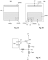
- FIGS. 3A, 3B and 3C schematically illustrate an example of an embodiment of an electronic device comprising a discrete transistor 300 mounted on a printed circuit board 320.
- the Figures 3A and 3B are respectively a bottom view of the transistor 300 and a top view of the printed circuit board 320, and the Figure 3C is an equivalent electrical diagram of the device.
- transistor 300 is identical or similar to transistor 100 of the Figure 1A .
- the transistor 300 comprises a single pad 105 for connection to the source (S) of the transistor accessible outside the housing 101.
- the printed circuit board 320 is for its part identical or similar to the printed circuit board 220 of the Figure 2B . More particularly, in this example, the printed circuit board 320 comprises two disjoint source connection pads 125 and 129.
- the pad 125 constitutes a conduction source pad of the device, and the pad 129 constitutes a source control pad of the device.
- the pads 125 and 129 are intended, when mounting the transistor 300, to both be connected to the source connection pad 105 of the transistor.
- the lower face of the source connection pad 105 of the transistor 300 is fixed and electrically connected, for example by welding or soldering, both to the upper face of the pad 125 and to the upper face of pad 129.
- the pads 125 and 129 are electrically isolated from each other in the absence of the transistor 300 (before mounting the transistor on the printed circuit board).
- the source control pad 129 is adjacent to the gate connection pad 127 of the printed circuit board, that is to say it is separated laterally from the pad 127 only by the insulating material of the card. of the printed circuit board, and not by another conductive element of the printed circuit board.
- the distance between pad 127 and pad 129 is less than a tenth of the largest dimension of transistor 300.
- the printed circuit board 320 may also include conductive tracks (not detailed on the Figure 3B ), connecting the connection pads 123, 125, 127 and 129 to connection pads to other discrete components of the device or to external connection terminals of the device.
- conductive tracks not detailed on the Figure 3B
- the function of transistor 300 is to modulate or switch a current circulating between terminals A1 and A2 of the device.
- the device includes a circuit (not visible on the Figure 3B ) for controlling transistor 300, also mounted on printed circuit board 320, connected between terminals A3 and A4 of the device. More particularly, in the case of a GaN HEMT transistor or a MOS transistor, the control circuit applies a control voltage between the gate (via terminal A3) and the source (via of terminal A4) of the transistor to control the current circulating between the conduction terminals A1 (drain) and A2 (source) of the device.
- FIG. 3C is an equivalent electrical diagram of an electronic device comprising the transistor 300 of the Figure 3A and a control circuit 310 of this transistor, mounted on the printed circuit board 320 of the Figure 3B .
- the control circuit 310 comprises a first terminal B1 connected to terminal A3 (itself connected to the gate of transistor 300), and a second terminal B2 connected to terminal A4 (itself connected to the source of transistor 300) .
- FIG. 3C we have shown a series association of a first inductance L sp1 and a second inductance L sp2 , connecting the source (S) of transistor 300 to terminal A2, and a third inductance L ss connecting the midpoint N1 between the inductances L sp1 and L sp2 at terminal B2 of the control circuit 310.
- the inductance L sp1 corresponds to the parasitic inductance of all the conductive elements connecting the source (S) of the transistor 300 both to the pad 125 and to the pad 129 of the printed circuit board 320, namely the connection pad 105 of the transistor 300 in this example.
- the inductance L sp2 corresponds to the parasitic inductance of all the conductive elements connecting the connection pad 105 of the transistor 300 to the terminal A2, namely the connection pad 125 of the printed circuit card, and the conductive track(s) connecting pad 125 to terminal A2.
- the inductance L ss corresponds to the parasitic inductance of all the conductive elements connecting the connection pad 105 of the transistor 200 to terminal B2, namely the connection pad 129 of the printed circuit card, and the conductive track(s) connecting pad 129 to terminal A4 (as well as possibly the conductive track(s) connecting terminal A4 to terminal B2, the parasitic inductance of which is considered negligible in the example shown).
- An advantage of the embodiment described in relation to the Figures 3A, 3B and 3C is that it allows the use of a discrete transistor comprising a single connection pad of source accessible outside the transistor housing, and, by means of a simple modification of the conductive pattern of the printed circuit board to create a source control pad disjoint from the conduction source pad, to significantly reduce the parasitic inductance of source connection seen through both the transistor control circuit and the device power path.
- This allows, in relation to the configuration of the Figures 1A, 1B and 1C , to increase the switching speed of the transistor without increasing the risk of malfunctions (without using a component equipped with an additional control pad as in the example of Figures 2A, 2B and 2C ).
- the embodiments described are not limited to the aforementioned application to switching power converters, but can be applied more generally to any electronic device comprising a discrete transistor mounted on a printed circuit board.
- FIG. 3A and 3B an exemplary embodiment in which a single source control pad 129 is provided on the printed circuit board.
- several disjoint source control pads intended to be connected to the same source connection pad 105 of the transistor as the conduction source pad 125, can be provided on the printed circuit board.
- two separate source control pads arranged on either side of the conduction source pad 125 can be provided on the printed circuit board.
- the different source control pads on the printed circuit board can be connected to separate control circuits, or to the same control circuit.
Landscapes
- Engineering & Computer Science (AREA)
- Microelectronics & Electronic Packaging (AREA)
- Manufacturing & Machinery (AREA)
- Electronic Switches (AREA)
- Semiconductor Integrated Circuits (AREA)
- Junction Field-Effect Transistors (AREA)
- Structures For Mounting Electric Components On Printed Circuit Boards (AREA)
Description
- La présente demande concerne un dispositif électronique, aussi appelé carte électronique, comportant un ou plusieurs transistors discrets montés sur une carte de circuit imprimé.
- De nombreux dispositifs électroniques comportant un ou plusieurs transistors discrets montés sur une carte de circuit imprimé ont déjà été proposés. On s'intéresse ici plus particulièrement à des convertisseurs de puissance dans lesquels un ou plusieurs transistors discrets montés sur une carte de circuit imprimé sont commandés en commutation à une fréquence relativement élevée, dite fréquence de découpage, par exemple une fréquence supérieure à 10 kHz. Dans un tel convertisseur, il est souhaitable que la vitesse de commutation (vitesse d'ouverture et vitesse de fermeture) des transistors soit la plus élevée possible. Ceci permet en effet d'augmenter la fréquence de commutation des transistors, et par conséquent de réduire les dimensions d'un ou plusieurs composants passifs (inductance(s) et/ou condensateur(s)) du convertisseur, tout en maintenant les pertes du convertisseur à un niveau relativement faible. En pratique, la vitesse de commutation des transistors est toutefois limitée, en raison notamment des inductances parasites des éléments conducteurs de connexion reliant le transistor à un circuit de contrôle du transistor.
-
US2012236516 concerne un composant transistor discret à effet de champ (FET) étant encapsulé dans un boîtier en un matériau isolant laissant accessible des plots de connexion correspondant aux bornes de conduction du transistor source (S), Drain (D) et Grille (G). Ce transistor est connecté à un circuit imprimé de façon à ce que la borne source (S), qui est plus large que les autres bornes, contacte plusieurs plots de connexion de la carte de circuit imprimé. Le circuit imprimé connecte deux plots de connexion soudés à une seule borne du transistor pour aider à l'alignement de celui-ci lors de la soudure grâce à la tension de superficie de la pâte à soudure. -
US2006113657 concerne des composants transistors discrets à effet de champ (FET) et un circuit de contrôle connecté aux bornes de commande (G) des transistors et aussi et à leur première borne de conduction (S). La réduction d'inductances parasites de la connexion du transistor se réalise par l'optimisation des distances de connexion entre le circuit de contrôle et les transistors ce qui a pour effet de réduire les résistances et le inductances de connexion. - Ces caractéristiques et leurs avantages, ainsi que d'autres, seront exposés en détail dans la description suivante de modes de réalisation particuliers faite à titre non limitatif en relation avec les figures jointes parmi lesquelles :
- la
figure 1A est une vue de dessous schématique d'un exemple d'un transistor discret ; - la
figure 1B est une vue de dessus schématique et partielle d'un exemple d'une carte de circuit imprimé destinée à recevoir le transistor de lafigure 1A ; - la
figure 1C est un schéma électrique équivalent d'un dispositif électronique comportant le transistor de lafigure 1A et un circuit de commande de ce transistor, montés sur la carte de circuit imprimé de lafigure 1B ; - la
figure 2A est une vue de dessous schématique d'un autre exemple d'un transistor discret ; - la
figure 2B est une vue de dessus schématique et partielle d'un exemple d'une carte de circuit imprimé destinée à recevoir le transistor de lafigure 2A ; - la
figure 2C est un schéma électrique équivalent d'un dispositif électronique comportant le transistor de lafigure 2A et un circuit de commande de ce transistor, montés sur la carte de circuit imprimé de lafigure 2B ; - la
figure 3A est une vue de dessous schématique d'un exemple d'un transistor discret d'un dispositif électronique selon un mode de réalisation ; - la
figure 3B est une vue de dessus schématique et partielle d'un exemple d'une carte de circuit imprimé d'un dispositif électronique selon un mode de réalisation, destinée à recevoir le transistor de lafigure 3A ; et - la
figure 3C est un schéma électrique équivalent d'un dispositif électronique selon un mode de réalisation, comportant le transistor de lafigure 3A et un circuit de commande de ce transistor, montés sur la carte de circuit imprimé de lafigure 3B . - De mêmes éléments ont été désignés par de mêmes références dans les différentes figures et, de plus, les diverses figures ne sont pas tracées à l'échelle. Par souci de clarté, seuls les éléments utiles à la compréhension des modes de réalisation décrits ont été représentés et sont détaillés. En particulier, la structure interne des transistors des dispositifs électroniques décrits n'a pas été détaillée, les modes de réalisation décrits étant compatibles avec toutes ou la plupart des structures connues de transistors discrets. De plus, les schémas électriques complets des dispositifs électroniques décrits n'ont pas été détaillés, les modes de réalisation décrits étant compatibles avec tous ou la plupart des dispositifs électroniques comportant des transistors discrets, et en particulier des transistors discrets commandés en commutation, par exemple des convertisseurs à découpage.
- On notera que par transistor discret, on entend ici un transistor formé dans et sur une puce semiconductrice indépendante des autres composants du dispositif. Un tel transistor peut en outre comprendre un boîtier d'encapsulation, par exemple en un matériau isolant, laissant accessibles au moins trois plots conducteurs de connexion à un dispositif extérieur, connectés respectivement aux deux bornes de conduction du transistor (la source et le drain dans le cas d'un transistor MOS ou dans le cas d'un transistor HEMT (de l'anglais "High Electron Mobility Transistor" - transistor à haute mobilité d'électrons), par exemple un transistor HEMT au nitrure de gallium (GaN)) et à une borne de commande du transistor (la grille dans le cas d'un transistor MOS ou dans le cas d'un transistor HEMT au GaN). Bien que les modes de réalisation décrits ne se limitent pas à ce cas particulier, on s'intéresse ici plus particulièrement à des transistors de puissance, c'est-à-dire des transistors adaptés à tenir des tensions relativement élevées à l'état ouvert (bloqué), par exemple des tensions supérieures ou égales à 100 V et de préférence supérieures ou égales à 500 V, et/ou à laisser passer des courants relativement élevés à l'état fermé (passant), par exemple des courants supérieurs ou égaux à 1 A et de préférence supérieurs ou égaux à 10 A.
- Par ailleurs, on entend ici par carte de circuit imprimé ou PCB (de l'anglais "Printed Circuit Board") un support en forme de plaque permettant de maintenir et de relier électriquement entre eux une pluralité de composants électroniques discrets, dans le but de réaliser un dispositif électronique complexe aussi appelé carte électronique. Une carte de circuit imprimé est par exemple constituée d'un empilement d'une couche support en un matériau isolant, et d'une ou plusieurs couches conductrices, par exemple en cuivre, séparées les unes des autres par un matériau isolant. Les couches conductrices sont localement gravées, par exemple par un procédé chimique, pour définir un ensemble de plots conducteurs de connexion auxquels sont destinés à être soudés ou brasés des plots conducteurs de connexion correspondants des composants du dispositif, et un ensemble de pistes conductrices reliant entre eux les plots de connexion de la carte de circuit imprimé.
- Dans la description qui suit, lorsque l'on fait référence à des qualificatifs de position absolue, tels que les termes "avant", "arrière", "haut", "bas", "gauche", "droite", etc., ou relative, tels que les termes "dessus", "dessous", "supérieur", "inférieur", etc., ou à des qualificatifs d'orientation, tels que les termes "horizontal", "vertical", etc., il est fait référence à l'orientation des figures, étant entendu que, en pratique, les dispositifs décrits peuvent être orientés différemment. Sauf précision contraire, les expressions "approximativement", "sensiblement", et "de l'ordre de" signifient à 10 % près, de préférence à 5 % près.
- La
figure 1A est une vue de dessous schématique d'un exemple d'un transistor discret 100. Le transistor 100 comprend une puce semiconductrice (non visible sur lafigure 1A ) dans et sur laquelle est formée la partie active du transistor. Dans cet exemple, la puce semiconductrice est encapsulée dans un boîtier 101 en un matériau isolant, par exemple en résine, laissant accessibles uniquement trois plots 103, 105 et 107 de connexion du transistor à un dispositif extérieur. Les plots 103, 105 et 107 sont par exemple en métal, par exemple en cuivre. Dans cet exemple, le transistor 100 est un transistor HEMT au GaN ou un transistor MOS, les plots 103, 105 et 107 étant respectivement connectés, à l'intérieur du boîtier 101, au drain, à la source et à la grille du transistor. Dans cet exemple, le boîtier 101 a une forme générale parallélépipédique, tous les plots de connexion du transistor à un dispositif extérieur étant disposés du côté de la face inférieure du transistor (la face visible sur lafigure 1A ). - La
figure 1B est une vue de dessus schématique et partielle d'un exemple d'une carte de circuit imprimé 120 destinée à recevoir le transistor 100 de lafigure 1A . La carte de circuit imprimé 120 comprend, du côté de sa face supérieure, trois plots de connexion 123, 125 et 127, par exemple en métal, par exemple en cuivre, destinés à être connectés respectivement aux trois plots de connexion 103, 105 et 107 du transistor 100. Dans cet exemple, les plots 123, 125 et 127 de la carte de circuit imprimé 120 ont, vus de face, sensiblement la même forme et les mêmes dimensions que, respectivement, les plots 103, 105 et 107 du transistor 100. Dans cet exemple, le transistor 100 et la carte de circuit imprimé 120 sont destinés à être assemblés par montage en surface. Autrement dit, la face inférieure de chacun des plots de connexion 103, 105 et 107 du transistor est fixée et connectée électriquement, par exemple par soudure ou par brasure, à la face supérieure du plot de connexion correspondant 123, respectivement 125, respectivement 127 de la carte de circuit imprimé 120. - La carte de circuit imprimé 120 peut en outre comprendre des pistes conductrices (non détaillées sur la
figure 1B ), reliant les plots de connexion 123, 125 et 127 à des plots de connexion à d'autres composants discrets du dispositif ou à des bornes de connexion extérieures du dispositif. Par souci de simplification, sur lafigure 1B , on a simplement représenté de façon schématique une borne A1 de la carte de circuit imprimé 120, à laquelle est connecté le plot 123 (correspondant au drain du transistor), une borne A2 de la carte de circuit imprimé 120, à laquelle est connecté le plot 125 (correspondant à la source du transistor), et une borne A3 de la carte de circuit imprimé 120, à laquelle est connecté le plot 127 (correspondant à la grille du transistor). En utilisation, le transistor 100 a pour fonction de moduler ou de commuter un courant circulant entre les bornes A1 et A2 du dispositif. Pour cela, le dispositif comprend un circuit (non visible sur lafigure 1B ) de contrôle du transistor 100, également monté sur la carte de circuit imprimé 120 et connecté entre les bornes A3 et A2 du dispositif. Plus particulièrement, dans le cas d'un transistor HEMT au GaN ou d'un transistor MOS, le circuit de contrôle applique une tension de commande entre la grille (par l'intermédiaire de la borne A3) et la source (par l'intermédiaire de la borne A2) du transistor pour contrôler le courant circulant entre les bornes de conduction (drain et source) du transistor. - La
figure 1C est un schéma électrique équivalent d'un dispositif électronique comportant le transistor 100 de lafigure 1A et un circuit de contrôle 110 de ce transistor, montés sur la carte de circuit imprimé 120 de lafigure 1B . Le circuit de contrôle 110 comprend une première borne B1 connectée à la borne A3 (elle-même connectée à la grille du transistor 100), et une deuxième borne B2 connectée à la borne A2 (elle-même connectée à la source du transistor 100). Sur lafigure 1C , on a représenté une première inductance Lsp, reliant la source (S) du transistor 100 à la borne A2, et une deuxième inductance Lss reliant la borne A2 à la borne B2 du circuit de contrôle 110. L'inductance Lsp correspond à l'inductance parasite de l'ensemble des éléments conducteurs reliant la source (S) du transistor 100 à la borne A2, à savoir le plot de connexion 105 du transistor, le plot de connexion correspondant 125 de la carte de circuit imprimé, et la ou les pistes conductrices reliant le plot 125 à la borne A2. L'inductance Lss correspond quant à elle à l'inductance parasite de l'ensemble des éléments conducteurs (non détaillés sur les figures) reliant la borne A2 du dispositif à la borne B2 du circuit de commande. - Bien que les inductances parasites Lsp et Lss soient très faibles, ces dernières peuvent perturber la tension grille-source effectivement vue par le transistor. En particulier, en fonctionnement, l'inductance Lsp est susceptible d'être traversée par des courants importants dans la mesure où elle se situe sur le chemin de puissance principal du transistor. Lors des commutations à l'état ouvert ou à l'état fermé du transistor, une variation rapide du courant circulant dans l'inductance Lsp se produit, ce qui peut générer une tension relativement élevée aux bornes de l'inductance Lsp. A titre d'exemple, pour une commutation d'un courant de 50 A en une période de commutation de 5 ns, la vitesse de variation du courant dans l'inductance Lsp est de 50 kA/ps. En considérant une inductance Lsp de 1 nH (ce qui correspond à une longueur de piste conductrice de l'ordre de 1 mm sur une carte de circuit imprimé), la tension aux bornes de l'inductance Lsp pendant la période de commutation peut atteindre 10 V. Ainsi, la tension de commande effectivement vue par le transistor est fortement influencée par l'inductance parasite Lsp, ce qui peut conduire à des dysfonctionnements, voire à un claquage du transistor.
- L'inductance Lss est quant à elle moins gênante dans la mesure où les courants qui la traversent sont en pratique négligeables par rapport au courant traversant l'inductance Lsp.
- Une solution pour limiter les dysfonctionnements évoqués ci-dessus est de limiter la vitesse de commutation du transistor. Comme indiqué ci-dessus, dans un convertisseur à découpage, ceci implique une diminution de la fréquence de découpage et par conséquent une augmentation des dimensions des composants passifs du convertisseur, ainsi qu'une augmentation des pertes de commutation.
- La
figure 2A est une vue de dessous schématique d'un autre exemple d'un transistor discret 200. Le transistor 200 comprend les mêmes éléments que le transistor 100 de lafigure 1A , agencés sensiblement de la même manière, et comprend en outre un plot supplémentaire 109 de connexion à un dispositif extérieur. Dans l'exemple représenté, le plot 109 est disposé sur la même face du boîtier 101 que les plots 103, 105 et 107, à savoir la face inférieure du boîtier. Le plot 109 est par exemple en le même matériau conducteur que les plots 103, 105 et 107. A l'intérieur du boîtier 101, le plot 109 est connecté à la région de source du transistor. A titre d'exemple, à l'intérieur du boîtier, le plot 109 (SS) est connecté à la même borne de source que le plot 105. Vu de l'extérieur, le plot 109 est toutefois isolé latéralement du plot 105 par le matériau isolant du boîtier 101. Le plot 109 constitue un plot de contrôle de source, destiné à être connecté au circuit de contrôle du transistor, tandis que le plot 105 constitue un plot de source de conduction, destiné à être connecté sur le chemin de puissance du dispositif. - La
figure 2B est une vue de dessus schématique et partielle d'un exemple d'une carte de circuit imprimé 220 destinée à recevoir le transistor 200 de lafigure 2A . La carte de circuit imprimé 220 comprend, du côté de sa face supérieure, quatre plots de connexion 123, 125, 127 et 129, par exemple en métal, par exemple en cuivre, destinés à être connectés respectivement aux quatre plots de connexion 103, 105, 107 et 109 du transistor 200. Dans cet exemple, les plots 123, 125, 127 et 129 de la carte de circuit imprimé 220 ont, vus de face, sensiblement la même forme et les mêmes dimensions que, respectivement, les plots 103, 105, 107 et 109 du transistor 200. Dans cet exemple, les plots 129 et 125 sont disjoints, c'est-à-dire que, en l'absence du transistor 200 (avant montage du transistor 200 sur la carte de circuit imprimé), les plots 129 et 125 sont électriquement isolés l'un de l'autre. - Dans cet exemple, le transistor 200 et la carte de circuit imprimé 220 sont destinés à être assemblés par montage en surface. Autrement dit, la face inférieure de chacun des plots de connexion 103, 105, 107 et 109 du transistor est fixée et connectée électriquement, par exemple par soudure ou par brasure, à la face supérieure du plot de connexion correspondant 123, respectivement 125, respectivement 127, respectivement 129 de la carte de circuit imprimé 220.
- La carte de circuit imprimé 220 peut en outre comprendre des pistes conductrices (non détaillées sur la
figure 2B ), reliant les plots de connexion 123, 125, 127 et 129 à des plots de connexion à d'autres composants discrets du dispositif ou à des bornes de connexion extérieures du dispositif. Par souci de simplification, sur lafigure 2B , on a simplement représenté de façon schématique une borne A1 de la carte de circuit imprimé 220, à laquelle est connecté le plot 123, une borne A2 de la carte de circuit imprimé 220, à laquelle est connecté le plot 125, une borne A3 de la carte de circuit imprimé 220, à laquelle est connecté le plot 127, et une borne A4 de la carte de circuit imprimé 220, à laquelle est connecté le plot 129. En utilisation, le transistor 200 a pour fonction de moduler ou de commuter un courant circulant entre les bornes A1 et A2 du dispositif. Pour cela, le dispositif comprend un circuit (non visible sur lafigure 2B ) de contrôle du transistor 200, également monté sur la carte de circuit imprimé 220, connecté entre les bornes A3 et A4 du dispositif. Plus particulièrement, dans le cas d'un transistor HEMT au GaN ou d'un transistor MOS, le circuit de contrôle applique une tension de commande entre la grille (par l'intermédiaire de la borne A3) et la source (par l'intermédiaire de la borne A4) du transistor pour contrôler le courant circulant entre les bornes de conduction A1 (drain) et A2 (source) du dispositif. - La
figure 2C est un schéma électrique équivalent d'un dispositif électronique comportant le transistor 200 de lafigure 2A et un circuit de contrôle 210 de ce transistor, montés sur la carte de circuit imprimé 220 de lafigure 2B . Le circuit de contrôle 210 comprend une première borne B1 connectée à la borne A3 (elle-même connectée à la grille du transistor 200), et une deuxième borne B2 connectée à la borne A4 (elle-même connectée à la source du transistor 200). Sur lafigure 2C , on a représenté une première inductance Lsp, reliant la source (S) du transistor 200 à la borne A2, et une deuxième inductance Lss reliant la source (S) du transistor 200 à la borne B2 du circuit de contrôle 210. L'inductance Lsp correspond à l'inductance parasite de l'ensemble des éléments conducteurs reliant la source (S) du transistor 200 à la borne A2, à savoir le plot de connexion 105 du transistor, le plot de connexion correspondant 125 de la carte de circuit imprimé, et la ou les pistes conductrices reliant le plot 125 à la borne A2. L'inductance Lss correspond quant à elle à l'inductance parasite de l'ensemble des éléments conducteurs reliant la source (S) du transistor 200 à la borne B2, à savoir le plot de connexion 109 du transistor, le plot de connexion correspondant 129 de la carte de circuit imprimé, et la ou les pistes conductrices reliant le plot 129 à la borne A4 (ainsi qu'éventuellement la ou les pistes conductrices reliant la borne A4 à la borne B2, dont l'inductance parasite est considérée comme négligeable dans l'exemple représenté). - Comme l'illustre le schéma de la
figure 2C , la prévision, dans le transistor 200, d'un plot de contrôle de source 109 distinct du plot de source de conduction 105, et, sur la carte de circuit imprimé 220, d'un plot de contrôle de source correspondant 129 distinct du plot de source de conduction 125, permet de rendre négligeable l'inductance parasite de connexion de source vue à la fois par le circuit de contrôle 210 et par le chemin de puissance du dispositif. - Dans la configuration des
figures 2A, 2B et 2C , l'inductance Lsp est toujours susceptible d'être traversée par des courants importants, ce qui peut, comme expliqué ci-dessous en relation avec lafigure 1C , conduire à l'apparition d'une tension relativement élevée à ses bornes lors des commutations du transistor. Toutefois, à la différence de la configuration desfigures 1A, 1B et 1C , ceci ne perturbe pas la tension de commande effectivement vue par le transistor, dans la mesure où l'inductance Lsp est en dehors du chemin de connexion entre la borne B2 du circuit de contrôle et la source du transistor. - De même que dans la configuration des
figures 1A, 1B et 1C , l'inductance Lss est quant à elle peu gênante dans la mesure où les courants qui la traversent sont négligeables par rapport au courant traversant l'inductance Lsp. - Ainsi, la configuration des
figures 2A, 2B et 2C permet d'appliquer au transistor une vitesse de commutation plus élevée que dans la configuration desfigures 1A, 1B et 1C , sans augmenter les risques de dysfonctionnements. - Toutefois, un inconvénient de cette solution est qu'elle nécessite d'utiliser des transistors discrets spécifiques, munis d'un plot de contrôle supplémentaire (le plot 109 dans l'exemple de la
figure 2A ), qui ne sont pas toujours disponibles dans les catalogues des fabricants de composants semi-conducteurs. - Les
figures 3A, 3B et 3C illustrent de façon schématique un exemple d'un mode de réalisation d'un dispositif électronique comportant un transistor discret 300 monté sur une carte de circuit imprimé 320. Lesfigures 3A et 3B sont respectivement une vue de dessous du transistor 300 et une vue de dessus de la carte de circuit imprimé 320, et lafigure 3C est un schéma électrique équivalent du dispositif. - Dans cet exemple, le transistor 300 est identique ou similaire au transistor 100 de la
figure 1A . En particulier, dans cet exemple, le transistor 300 comprend un unique plot 105 de connexion à la source (S) du transistor accessible à l'extérieur du boîtier 101. - La carte de circuit imprimé 320 est quant à elle identique ou similaire à la carte de circuit imprimé 220 de la
figure 2B . Plus particulièrement, dans cet exemple, la carte de circuit imprimé 320 comprend deux plots de connexion de source 125 et 129 disjoints. Le plot 125 constitue un plot de source de conduction du dispositif, et le plot 129 constitue un plot de contrôle de source du dispositif. - Dans l'exemple des
figures 3A, 3B et 3C , les plots 125 et 129 sont destinés, lors du montage du transistor 300, à être tous deux connectés au plot de connexion de source 105 du transistor. - Autrement dit, lors du montage du transistor 300, la face inférieure du plot de connexion de source 105 du transistor 300 est fixée et connectée électriquement, par exemple par soudure ou par brasure, à la fois à la face supérieure du plot 125 et à la face supérieure du plot 129.
- De façon similaire à ce qui a été décrit dans l'exemple des
figures 2A, 2B et 2C , les plots 125 et 129 sont isolés électriquement l'un de l'autre en l'absence du transistor 300 (avant montage du transistor sur la carte de circuit imprimé). - De préférence, le plot de contrôle de source 129 est voisin du plot de connexion de grille 127 de la carte de circuit imprimé, c'est-à-dire qu'il est séparé latéralement du plot 127 uniquement par le matériau isolant de la carte de circuit imprimé, et non par un autre élément conducteur de la carte de circuit imprimé. A titre d'exemple, en vue de dessus, la distance entre le plot 127 et le plot 129 est inférieure au dixième de la plus grande dimension du transistor 300.
- La carte de circuit imprimé 320 peut en outre comprendre des pistes conductrices (non détaillées sur la
figure 3B ), reliant les plots de connexion 123, 125, 127 et 129 à des plots de connexion à d'autres composants discrets du dispositif ou à des bornes de connexion extérieures du dispositif. Par souci de simplification, sur lafigure 3B , on a simplement représenté de façon schématique une borne A1 de la carte de circuit imprimé 320, à laquelle est connecté le plot 123, une borne A2 de la carte de circuit imprimé 320, à laquelle est connecté le plot 125, une borne A3 de la carte de circuit imprimé 320, à laquelle est connecté le plot 127, et une borne A4 de la carte de circuit imprimé 320, à laquelle est connecté le plot 129. - En utilisation, le transistor 300 a pour fonction de moduler ou commuter un courant circulant entre les bornes A1 et A2 du dispositif. Pour cela, le dispositif comprend un circuit (non visible sur la
figure 3B ) de contrôle du transistor 300, également monté sur la carte de circuit imprimé 320, connecté entre les bornes A3 et A4 du dispositif. Plus particulièrement, dans le cas d'un transistor HEMT au GaN ou d'un transistor MOS, le circuit de contrôle applique une tension de commande entre la grille (par l'intermédiaire de la borne A3) et la source (par l'intermédiaire de la borne A4) du transistor pour contrôler le courant circulant entre les bornes de conduction A1 (drain) et A2 (source) du dispositif. - La
figure 3C est un schéma électrique équivalent d'un dispositif électronique comportant le transistor 300 de lafigure 3A et un circuit de contrôle 310 de ce transistor, montés sur la carte de circuit imprimé 320 de lafigure 3B . Le circuit de contrôle 310 comprend une première borne B1 connectée à la borne A3 (elle-même connectée à la grille du transistor 300), et une deuxième borne B2 connectée à la borne A4 (elle-même connectée à la source du transistor 300). Sur lafigure 3C , on a représenté une association en série d'une première inductance Lsp1 et d'une deuxième inductance Lsp2, reliant la source (S) du transistor 300 à la borne A2, et une troisième inductance Lss reliant le point milieu N1 entre les inductances Lsp1 et Lsp2 à la borne B2 du circuit de contrôle 310. L'inductance Lsp1 correspond à l'inductance parasite de l'ensemble des éléments conducteurs reliant la source (S) du transistor 300 à la fois au plot 125 et au plot 129 de la carte de circuit imprimé 320, à savoir le plot de connexion 105 du transistor 300 dans cet exemple. L'inductance Lsp2 correspond quant à elle à l'inductance parasite de l'ensemble des éléments conducteurs reliant le plot de connexion 105 du transistor 300 à la borne A2, à savoir le plot de connexion 125 de la carte de circuit imprimé, et la ou les pistes conductrices reliant le plot 125 à la borne A2. L'inductance Lss correspond quant à elle à l'inductance parasite de l'ensemble des éléments conducteurs reliant le plot de connexion 105 du transistor 200 à la borne B2, à savoir le plot de connexion 129 de la carte de circuit imprimé, et la ou les pistes conductrices reliant le plot 129 à la borne A4 (ainsi qu'éventuellement la ou les pistes conductrices reliant la borne A4 à la borne B2, dont l'inductance parasite est considérée comme négligeable dans l'exemple représenté). - Un avantage du mode de réalisation décrit en relation avec les
figures 3A, 3B et 3C est qu'il permet d'utiliser un transistor discret comportant un unique plot de connexion de source accessible à l'extérieur du boîtier du transistor, et, moyennant une simple modification du motif conducteur de la carte de circuit imprimé pour créer un plot de contrôle de source disjoint du plot de source de conduction, de réduire significativement l'inductance parasite de connexion de source vue à la fois par le circuit de contrôle du transistor et par le chemin de puissance du dispositif. Ceci permet, par rapport à la configuration desfigures 1A, 1B et 1C , d'augmenter la vitesse de commutation du transistor sans augmenter les risques de dysfonctionnements (sans pour autant utiliser un composant muni d'un plot de contrôle supplémentaire comme dans l'exemple desfigures 2A, 2B et 2C ). - Des modes de réalisation particuliers ont été décrits. Diverses variantes et modifications apparaîtront à l'homme de l'art. En particulier, on a décrit ci-dessus des exemples de réalisation appliqués à des transistors HEMT au GaN ou à des transistors MOS. Les modes de réalisation ne se limitent toutefois pas à ces cas particuliers. Plus généralement, les modes de réalisation décrits peuvent être appliqués à tout transistor comportant deux bornes de conduction et une borne de commande destinée à recevoir un signal électrique de commande référencé par rapport à l'une des bornes de conduction, par exemple des transistors bipolaires ou des transistors à effet de champ. Les modes de réalisation décrits sont notamment particulièrement adaptés aux transistors à commutation rapide. Outre les exemples mentionnés ci-dessus, les modes de réalisation décrits sont notamment particulièrement avantageux pour des transistors MOS au carbure de silicium ou pour des transistors MOS à superjonction silicium.
- De plus, les modes de réalisation décrits ne se limitent pas à l'application susmentionnée à des convertisseurs de puissance à découpage, mais peuvent s'appliquer plus généralement à tout dispositif électronique comportant un transistor discret monté sur une carte de circuit imprimé.
- Par ailleurs, on a représenté, en
figures 3A et 3B , un exemple de réalisation dans lequel un unique plot de contrôle de source 129 est prévu sur la carte de circuit imprimé. A titre de variante, plusieurs plots de contrôle de source disjoints, destinés à être connectés au même plot de connexion de source 105 du transistor que le plot de source de conduction 125, peuvent être prévus sur la carte de circuit imprimé. A titre d'exemple, deux plots de contrôle de source disjoints disposés de part et d'autre du plot de source de conduction 125 peuvent être prévus sur la carte de circuit imprimé. Les différents plots de contrôle de source de la carte de circuit imprimé peuvent être connectés à des circuits de contrôle distincts, ou à un même circuit de contrôle.
Claims (10)
- Dispositif électronique comportant :un transistor discret (300) comportant une puce semiconductrice encapsulée dans un boîtier (101) en un matériau isolant laissant accessible un premier plot (105) de connexion à une première borne de conduction (S) du transistor, un deuxième plot (103) de connexion à une deuxième borne de conduction (D) du transistor, et un troisième plot (107) de connexion à une borne de commande (G) du transistor ; etune carte de circuit imprimé (320) comportant des premier (125), deuxième (129), troisième (123) et quatrième (127) plots de connexion disjoints,dans lequel :- le transistor est monté sur la carte de circuit imprimé de façon que le premier plot de connexion (105) du transistor soit en contact avec les premier (125) et deuxième (129) plots de connexion de la carte de circuit imprimé et que les deuxième (103) et troisième (107) plots de connexion du transistor soient respectivement en contact avec les troisième (123) et quatrième (127) plots de connexion de la carte de circuit imprimé ;caractérisé en ce que- le dispositif comporte en outre, monté sur la carte de circuit imprimé (320), un circuit de contrôle (310) du transistor, connecté à la borne de commande (G) du transistor par l'intermédiaire du quatrième plot de connexion (127) de la carte de circuit imprimé et à la première borne de conduction (S) du transistor par l'intermédiaire du deuxième plot de connexion (129) de la carte de circuit imprimé ; et- le premier plot de connexion (125) de la carte de circuit imprimé est connecté à une borne de conduction de puissance (A2) du dispositif.
- Dispositif selon la revendication 1, dans lequel le circuit de contrôle (310) est configuré pour commuter alternativement le transistor (300) à l'état ouvert et à l'état fermé à une fréquence supérieure à 10 kHz.
- Dispositif selon la revendication 1 ou 2, dans lequel, en vue de dessus, la distance entre le deuxième plot de connexion (129) de la carte de circuit imprimé et le quatrième plot de connexion (127) de la carte de circuit imprimé est inférieure au dixième de la plus grande dimension du transistor (300) .
- Dispositif selon l'une quelconque des revendications 1 à 3, dans lequel :la carte de circuit imprimé comprend en outre un cinquième plot de connexion disjoint des premier (125) et deuxième (129) plots de connexion de la carte de circuit imprimé ;le transistor est monté sur la carte de circuit imprimé de façon que le premier plot de connexion (105) du transistor soit en contact avec les premier (125), deuxième (129) et cinquième plots de connexion de la carte de circuit imprimé ; etle cinquième plot de connexion de la carte de circuit imprimé étant connecté au circuit de contrôle (310) ou à un circuit de contrôle supplémentaire du transistor.
- Dispositif selon l'une quelconque des revendications 1 à 4, dans lequel les plots de connexion (103, 105, 107, 123, 125, 127, 129) sont en métal.
- Dispositif selon l'une quelconque des revendications 1 à 5, dans lequel les plots de connexion (103, 105, 107, 123, 125, 127, 129) sont en cuivre.
- Dispositif selon l'une quelconque des revendications 1 à 6, dans lequel le transistor (300) est un transistor MOS, la première borne de conduction (S) étant une borne de source du transistor.
- Dispositif selon la revendication 7 dans son rattachement à la revendication 2, dans lequel la deuxième borne de conduction (D) et la borne de commande (G) sont respectivement une borne de drain et une borne de grille du transistor.
- Dispositif selon l'une quelconque des revendications 1 à 8, dans lequel le transistor (300) est un transistor au nitrure de gallium, un transistor MOS au carbure de silicium, ou un transistor MOS à superjonction silicium.
- Dispositif selon l'une quelconque des revendications 1 à 9, dans lequel les premier (125), deuxième (129) et quatrième (127) plots de connexion de la carte de circuit imprimé (320) sont séparés par une région isolante en forme de F.
Applications Claiming Priority (1)
| Application Number | Priority Date | Filing Date | Title |
|---|---|---|---|
| FR1855665A FR3083046B1 (fr) | 2018-06-25 | 2018-06-25 | Dispositif electronique comportant un transistor discret monte sur une carte de circuit imprime |
Publications (2)
| Publication Number | Publication Date |
|---|---|
| EP3589091A1 EP3589091A1 (fr) | 2020-01-01 |
| EP3589091B1 true EP3589091B1 (fr) | 2024-08-07 |
Family
ID=63407457
Family Applications (1)
| Application Number | Title | Priority Date | Filing Date |
|---|---|---|---|
| EP19181822.8A Active EP3589091B1 (fr) | 2018-06-25 | 2019-06-21 | Dispositif électronique comportant un transistor discret monté sur une carte de circuit imprimé |
Country Status (3)
| Country | Link |
|---|---|
| US (1) | US10930606B2 (fr) |
| EP (1) | EP3589091B1 (fr) |
| FR (1) | FR3083046B1 (fr) |
Citations (1)
| Publication number | Priority date | Publication date | Assignee | Title |
|---|---|---|---|---|
| US20070170945A1 (en) * | 2006-01-26 | 2007-07-26 | Paul Skow | Printed circuit board and method of use thereof |
Family Cites Families (3)
| Publication number | Priority date | Publication date | Assignee | Title |
|---|---|---|---|---|
| US7721232B2 (en) * | 2004-11-29 | 2010-05-18 | Infineon Technologies Ag | Designated MOSFET and driver design to achieve lowest parasitics in discrete circuits |
| JP5017472B1 (ja) * | 2011-03-16 | 2012-09-05 | 株式会社東芝 | 電子機器 |
| US10135335B2 (en) * | 2016-08-22 | 2018-11-20 | Infineon Technologies Americas Corp. | Powerstage attached to inductor |
-
2018
- 2018-06-25 FR FR1855665A patent/FR3083046B1/fr active Active
-
2019
- 2019-06-21 EP EP19181822.8A patent/EP3589091B1/fr active Active
- 2019-06-23 US US16/449,405 patent/US10930606B2/en active Active
Patent Citations (1)
| Publication number | Priority date | Publication date | Assignee | Title |
|---|---|---|---|---|
| US20070170945A1 (en) * | 2006-01-26 | 2007-07-26 | Paul Skow | Printed circuit board and method of use thereof |
Also Published As
| Publication number | Publication date |
|---|---|
| FR3083046B1 (fr) | 2021-01-08 |
| EP3589091A1 (fr) | 2020-01-01 |
| US10930606B2 (en) | 2021-02-23 |
| US20190393174A1 (en) | 2019-12-26 |
| FR3083046A1 (fr) | 2019-12-27 |
Similar Documents
| Publication | Publication Date | Title |
|---|---|---|
| EP3545551B1 (fr) | Circuit integre forme d'un empilement de deux puces connectees en serie | |
| US6219254B1 (en) | Chip-to-board connection assembly and method therefor | |
| FR2591801A1 (fr) | Boitier d'encapsulation d'un circuit electronique | |
| FR2621173A1 (fr) | Boitier pour circuit integre de haute densite | |
| FR2609841A1 (fr) | Dispositif de circuit integre a semi-conducteurs | |
| FR2700416A1 (fr) | Dispositif à semiconducteurs comportant un élément semiconducteur sur un élément de montage. | |
| FR2529013A1 (fr) | Circuit a haute frequence et dispositif semi-conducteur pour equiper un tel circuit | |
| FR2625368A1 (fr) | Circuit integre monolithique micro-onde et procede de fabrication correspondant | |
| EP2466684A1 (fr) | Système d'antenne en diversité | |
| FR2911006A1 (fr) | Puce de circuit electronique integre comprenant une inductance | |
| EP3588556B1 (fr) | Composant électronique discret comprenant un transistor | |
| WO2018091852A1 (fr) | Circuit intégré forme de deux puces connectées en série | |
| EP3589091A1 (fr) | Dispositif électronique comportant un transistor discret monté sur une carte de circuit imprimé | |
| FR3005786A1 (fr) | Circuit cascode a deux transistors | |
| EP0053526B1 (fr) | Commutateur à commande par impulsions en ouverture et en fermeture, et son intégration | |
| EP3754697A1 (fr) | Composant monolithique comportant un transistor de puissance au nitrure de gallium | |
| EP0368741A1 (fr) | Support de circuit intégré et son procédé de fabrication, circuit intégré adapté au support et boîtiers en résultant | |
| EP0599739A1 (fr) | Thyristor et assemblage de thyristors à cathode commune | |
| FR2911005A1 (fr) | Transistor mos adapte a la tenue de forts courants | |
| FR2831328A1 (fr) | Protection d'un circuit integre contre des decharges electrostatiques et autres surtensions | |
| FR2879348A1 (fr) | Protection d'un condensateur integre | |
| EP3586360B1 (fr) | Composant electronique muni d'un transistor et de doigts interdigites pour former au moins une partie d'un composant capacitif au sein du composant electronique | |
| FR3079347A1 (fr) | Protection contre les decharges electrostatiques et filtrage | |
| EP4690304A1 (fr) | Module de puissance | |
| WO2023110966A1 (fr) | Bras de commutation utilisant une carte de circuit imprimé |
Legal Events
| Date | Code | Title | Description |
|---|---|---|---|
| PUAI | Public reference made under article 153(3) epc to a published international application that has entered the european phase |
Free format text: ORIGINAL CODE: 0009012 |
|
| STAA | Information on the status of an ep patent application or granted ep patent |
Free format text: STATUS: THE APPLICATION HAS BEEN PUBLISHED |
|
| AK | Designated contracting states |
Kind code of ref document: A1 Designated state(s): AL AT BE BG CH CY CZ DE DK EE ES FI FR GB GR HR HU IE IS IT LI LT LU LV MC MK MT NL NO PL PT RO RS SE SI SK SM TR |
|
| AX | Request for extension of the european patent |
Extension state: BA ME |
|
| STAA | Information on the status of an ep patent application or granted ep patent |
Free format text: STATUS: REQUEST FOR EXAMINATION WAS MADE |
|
| 17P | Request for examination filed |
Effective date: 20200127 |
|
| RBV | Designated contracting states (corrected) |
Designated state(s): AL AT BE BG CH CY CZ DE DK EE ES FI FR GB GR HR HU IE IS IT LI LT LU LV MC MK MT NL NO PL PT RO RS SE SI SK SM TR |
|
| STAA | Information on the status of an ep patent application or granted ep patent |
Free format text: STATUS: EXAMINATION IS IN PROGRESS |
|
| 17Q | First examination report despatched |
Effective date: 20210419 |
|
| RAP3 | Party data changed (applicant data changed or rights of an application transferred) |
Owner name: RENAULT S.A.S Owner name: COMMISSARIAT A L'ENERGIE ATOMIQUE ET AUX ENERGIES ALTERNATIVES |
|
| RAP3 | Party data changed (applicant data changed or rights of an application transferred) |
Owner name: RENAULT S.A.S Owner name: COMMISSARIAT A L'ENERGIE ATOMIQUE ET AUX ENERGIES ALTERNATIVES |
|
| P01 | Opt-out of the competence of the unified patent court (upc) registered |
Effective date: 20230530 |
|
| GRAP | Despatch of communication of intention to grant a patent |
Free format text: ORIGINAL CODE: EPIDOSNIGR1 |
|
| STAA | Information on the status of an ep patent application or granted ep patent |
Free format text: STATUS: GRANT OF PATENT IS INTENDED |
|
| RIC1 | Information provided on ipc code assigned before grant |
Ipc: H03F 3/00 20060101ALN20240221BHEP Ipc: H05K 1/11 20060101ALN20240221BHEP Ipc: H05K 1/02 20060101ALN20240221BHEP Ipc: H05K 3/34 20060101AFI20240221BHEP |
|
| RIC1 | Information provided on ipc code assigned before grant |
Ipc: H03F 3/00 20060101ALN20240228BHEP Ipc: H05K 1/11 20060101ALN20240228BHEP Ipc: H05K 1/02 20060101ALN20240228BHEP Ipc: H05K 3/34 20060101AFI20240228BHEP |
|
| INTG | Intention to grant announced |
Effective date: 20240315 |
|
| GRAS | Grant fee paid |
Free format text: ORIGINAL CODE: EPIDOSNIGR3 |
|
| GRAA | (expected) grant |
Free format text: ORIGINAL CODE: 0009210 |
|
| STAA | Information on the status of an ep patent application or granted ep patent |
Free format text: STATUS: THE PATENT HAS BEEN GRANTED |
|
| AK | Designated contracting states |
Kind code of ref document: B1 Designated state(s): AL AT BE BG CH CY CZ DE DK EE ES FI FR GB GR HR HU IE IS IT LI LT LU LV MC MK MT NL NO PL PT RO RS SE SI SK SM TR |
|
| REG | Reference to a national code |
Ref country code: GB Ref legal event code: FG4D Free format text: NOT ENGLISH |
|
| REG | Reference to a national code |
Ref country code: CH Ref legal event code: EP |
|
| REG | Reference to a national code |
Ref country code: IE Ref legal event code: FG4D Free format text: LANGUAGE OF EP DOCUMENT: FRENCH |
|
| REG | Reference to a national code |
Ref country code: DE Ref legal event code: R096 Ref document number: 602019056457 Country of ref document: DE |
|
| RAP4 | Party data changed (patent owner data changed or rights of a patent transferred) |
Owner name: RENAULT S.A.S Owner name: COMMISSARIAT A L'ENERGIE ATOMIQUE ET AUX ENERGIESALTERNATIVES |
|
| REG | Reference to a national code |
Ref country code: LT Ref legal event code: MG9D |
|
| REG | Reference to a national code |
Ref country code: NL Ref legal event code: MP Effective date: 20240807 |
|
| PG25 | Lapsed in a contracting state [announced via postgrant information from national office to epo] |
Ref country code: NO Free format text: LAPSE BECAUSE OF FAILURE TO SUBMIT A TRANSLATION OF THE DESCRIPTION OR TO PAY THE FEE WITHIN THE PRESCRIBED TIME-LIMIT Effective date: 20241107 |
|
| REG | Reference to a national code |
Ref country code: AT Ref legal event code: MK05 Ref document number: 1712318 Country of ref document: AT Kind code of ref document: T Effective date: 20240807 |
|
| PG25 | Lapsed in a contracting state [announced via postgrant information from national office to epo] |
Ref country code: NL Free format text: LAPSE BECAUSE OF FAILURE TO SUBMIT A TRANSLATION OF THE DESCRIPTION OR TO PAY THE FEE WITHIN THE PRESCRIBED TIME-LIMIT Effective date: 20240807 Ref country code: FI Free format text: LAPSE BECAUSE OF FAILURE TO SUBMIT A TRANSLATION OF THE DESCRIPTION OR TO PAY THE FEE WITHIN THE PRESCRIBED TIME-LIMIT Effective date: 20240807 Ref country code: GR Free format text: LAPSE BECAUSE OF FAILURE TO SUBMIT A TRANSLATION OF THE DESCRIPTION OR TO PAY THE FEE WITHIN THE PRESCRIBED TIME-LIMIT Effective date: 20241108 Ref country code: PL Free format text: LAPSE BECAUSE OF FAILURE TO SUBMIT A TRANSLATION OF THE DESCRIPTION OR TO PAY THE FEE WITHIN THE PRESCRIBED TIME-LIMIT Effective date: 20240807 Ref country code: PT Free format text: LAPSE BECAUSE OF FAILURE TO SUBMIT A TRANSLATION OF THE DESCRIPTION OR TO PAY THE FEE WITHIN THE PRESCRIBED TIME-LIMIT Effective date: 20241209 |
|
| PG25 | Lapsed in a contracting state [announced via postgrant information from national office to epo] |
Ref country code: BG Free format text: LAPSE BECAUSE OF FAILURE TO SUBMIT A TRANSLATION OF THE DESCRIPTION OR TO PAY THE FEE WITHIN THE PRESCRIBED TIME-LIMIT Effective date: 20240807 |
|
| PG25 | Lapsed in a contracting state [announced via postgrant information from national office to epo] |
Ref country code: LV Free format text: LAPSE BECAUSE OF FAILURE TO SUBMIT A TRANSLATION OF THE DESCRIPTION OR TO PAY THE FEE WITHIN THE PRESCRIBED TIME-LIMIT Effective date: 20240807 |
|
| PG25 | Lapsed in a contracting state [announced via postgrant information from national office to epo] |
Ref country code: AT Free format text: LAPSE BECAUSE OF FAILURE TO SUBMIT A TRANSLATION OF THE DESCRIPTION OR TO PAY THE FEE WITHIN THE PRESCRIBED TIME-LIMIT Effective date: 20240807 Ref country code: IS Free format text: LAPSE BECAUSE OF FAILURE TO SUBMIT A TRANSLATION OF THE DESCRIPTION OR TO PAY THE FEE WITHIN THE PRESCRIBED TIME-LIMIT Effective date: 20241207 |
|
| PG25 | Lapsed in a contracting state [announced via postgrant information from national office to epo] |
Ref country code: HR Free format text: LAPSE BECAUSE OF FAILURE TO SUBMIT A TRANSLATION OF THE DESCRIPTION OR TO PAY THE FEE WITHIN THE PRESCRIBED TIME-LIMIT Effective date: 20240807 |
|
| PG25 | Lapsed in a contracting state [announced via postgrant information from national office to epo] |
Ref country code: ES Free format text: LAPSE BECAUSE OF FAILURE TO SUBMIT A TRANSLATION OF THE DESCRIPTION OR TO PAY THE FEE WITHIN THE PRESCRIBED TIME-LIMIT Effective date: 20240807 Ref country code: RS Free format text: LAPSE BECAUSE OF FAILURE TO SUBMIT A TRANSLATION OF THE DESCRIPTION OR TO PAY THE FEE WITHIN THE PRESCRIBED TIME-LIMIT Effective date: 20241107 |
|
| PG25 | Lapsed in a contracting state [announced via postgrant information from national office to epo] |
Ref country code: RS Free format text: LAPSE BECAUSE OF FAILURE TO SUBMIT A TRANSLATION OF THE DESCRIPTION OR TO PAY THE FEE WITHIN THE PRESCRIBED TIME-LIMIT Effective date: 20241107 Ref country code: PT Free format text: LAPSE BECAUSE OF FAILURE TO SUBMIT A TRANSLATION OF THE DESCRIPTION OR TO PAY THE FEE WITHIN THE PRESCRIBED TIME-LIMIT Effective date: 20241209 Ref country code: PL Free format text: LAPSE BECAUSE OF FAILURE TO SUBMIT A TRANSLATION OF THE DESCRIPTION OR TO PAY THE FEE WITHIN THE PRESCRIBED TIME-LIMIT Effective date: 20240807 Ref country code: NO Free format text: LAPSE BECAUSE OF FAILURE TO SUBMIT A TRANSLATION OF THE DESCRIPTION OR TO PAY THE FEE WITHIN THE PRESCRIBED TIME-LIMIT Effective date: 20241107 Ref country code: NL Free format text: LAPSE BECAUSE OF FAILURE TO SUBMIT A TRANSLATION OF THE DESCRIPTION OR TO PAY THE FEE WITHIN THE PRESCRIBED TIME-LIMIT Effective date: 20240807 Ref country code: LV Free format text: LAPSE BECAUSE OF FAILURE TO SUBMIT A TRANSLATION OF THE DESCRIPTION OR TO PAY THE FEE WITHIN THE PRESCRIBED TIME-LIMIT Effective date: 20240807 Ref country code: IS Free format text: LAPSE BECAUSE OF FAILURE TO SUBMIT A TRANSLATION OF THE DESCRIPTION OR TO PAY THE FEE WITHIN THE PRESCRIBED TIME-LIMIT Effective date: 20241207 Ref country code: HR Free format text: LAPSE BECAUSE OF FAILURE TO SUBMIT A TRANSLATION OF THE DESCRIPTION OR TO PAY THE FEE WITHIN THE PRESCRIBED TIME-LIMIT Effective date: 20240807 Ref country code: GR Free format text: LAPSE BECAUSE OF FAILURE TO SUBMIT A TRANSLATION OF THE DESCRIPTION OR TO PAY THE FEE WITHIN THE PRESCRIBED TIME-LIMIT Effective date: 20241108 Ref country code: FI Free format text: LAPSE BECAUSE OF FAILURE TO SUBMIT A TRANSLATION OF THE DESCRIPTION OR TO PAY THE FEE WITHIN THE PRESCRIBED TIME-LIMIT Effective date: 20240807 Ref country code: ES Free format text: LAPSE BECAUSE OF FAILURE TO SUBMIT A TRANSLATION OF THE DESCRIPTION OR TO PAY THE FEE WITHIN THE PRESCRIBED TIME-LIMIT Effective date: 20240807 Ref country code: BG Free format text: LAPSE BECAUSE OF FAILURE TO SUBMIT A TRANSLATION OF THE DESCRIPTION OR TO PAY THE FEE WITHIN THE PRESCRIBED TIME-LIMIT Effective date: 20240807 Ref country code: AT Free format text: LAPSE BECAUSE OF FAILURE TO SUBMIT A TRANSLATION OF THE DESCRIPTION OR TO PAY THE FEE WITHIN THE PRESCRIBED TIME-LIMIT Effective date: 20240807 |
|
| PG25 | Lapsed in a contracting state [announced via postgrant information from national office to epo] |
Ref country code: SM Free format text: LAPSE BECAUSE OF FAILURE TO SUBMIT A TRANSLATION OF THE DESCRIPTION OR TO PAY THE FEE WITHIN THE PRESCRIBED TIME-LIMIT Effective date: 20240807 Ref country code: DK Free format text: LAPSE BECAUSE OF FAILURE TO SUBMIT A TRANSLATION OF THE DESCRIPTION OR TO PAY THE FEE WITHIN THE PRESCRIBED TIME-LIMIT Effective date: 20240807 Ref country code: RO Free format text: LAPSE BECAUSE OF FAILURE TO SUBMIT A TRANSLATION OF THE DESCRIPTION OR TO PAY THE FEE WITHIN THE PRESCRIBED TIME-LIMIT Effective date: 20240807 |
|
| PG25 | Lapsed in a contracting state [announced via postgrant information from national office to epo] |
Ref country code: EE Free format text: LAPSE BECAUSE OF FAILURE TO SUBMIT A TRANSLATION OF THE DESCRIPTION OR TO PAY THE FEE WITHIN THE PRESCRIBED TIME-LIMIT Effective date: 20240807 |
|
| PG25 | Lapsed in a contracting state [announced via postgrant information from national office to epo] |
Ref country code: CZ Free format text: LAPSE BECAUSE OF FAILURE TO SUBMIT A TRANSLATION OF THE DESCRIPTION OR TO PAY THE FEE WITHIN THE PRESCRIBED TIME-LIMIT Effective date: 20240807 |
|
| PG25 | Lapsed in a contracting state [announced via postgrant information from national office to epo] |
Ref country code: SK Free format text: LAPSE BECAUSE OF FAILURE TO SUBMIT A TRANSLATION OF THE DESCRIPTION OR TO PAY THE FEE WITHIN THE PRESCRIBED TIME-LIMIT Effective date: 20240807 |
|
| REG | Reference to a national code |
Ref country code: DE Ref legal event code: R097 Ref document number: 602019056457 Country of ref document: DE |
|
| PLBE | No opposition filed within time limit |
Free format text: ORIGINAL CODE: 0009261 |
|
| STAA | Information on the status of an ep patent application or granted ep patent |
Free format text: STATUS: NO OPPOSITION FILED WITHIN TIME LIMIT |
|
| PGFP | Annual fee paid to national office [announced via postgrant information from national office to epo] |
Ref country code: DE Payment date: 20250618 Year of fee payment: 7 |
|
| PGFP | Annual fee paid to national office [announced via postgrant information from national office to epo] |
Ref country code: GB Payment date: 20250618 Year of fee payment: 7 |
|
| 26N | No opposition filed |
Effective date: 20250508 |
|
| PGFP | Annual fee paid to national office [announced via postgrant information from national office to epo] |
Ref country code: FR Payment date: 20250623 Year of fee payment: 7 |
|
| PG25 | Lapsed in a contracting state [announced via postgrant information from national office to epo] |
Ref country code: SE Free format text: LAPSE BECAUSE OF FAILURE TO SUBMIT A TRANSLATION OF THE DESCRIPTION OR TO PAY THE FEE WITHIN THE PRESCRIBED TIME-LIMIT Effective date: 20240807 |
|
| REG | Reference to a national code |
Ref country code: CH Ref legal event code: H13 Free format text: ST27 STATUS EVENT CODE: U-0-0-H10-H13 (AS PROVIDED BY THE NATIONAL OFFICE) Effective date: 20260127 |
|
| PG25 | Lapsed in a contracting state [announced via postgrant information from national office to epo] |
Ref country code: IT Free format text: LAPSE BECAUSE OF FAILURE TO SUBMIT A TRANSLATION OF THE DESCRIPTION OR TO PAY THE FEE WITHIN THE PRESCRIBED TIME-LIMIT Effective date: 20240807 |
|
| PG25 | Lapsed in a contracting state [announced via postgrant information from national office to epo] |
Ref country code: MC Free format text: LAPSE BECAUSE OF FAILURE TO SUBMIT A TRANSLATION OF THE DESCRIPTION OR TO PAY THE FEE WITHIN THE PRESCRIBED TIME-LIMIT Effective date: 20240807 |
|
| PG25 | Lapsed in a contracting state [announced via postgrant information from national office to epo] |
Ref country code: LU Free format text: LAPSE BECAUSE OF NON-PAYMENT OF DUE FEES Effective date: 20250621 |
|
| REG | Reference to a national code |
Ref country code: BE Ref legal event code: MM Effective date: 20250630 |
|
| PG25 | Lapsed in a contracting state [announced via postgrant information from national office to epo] |
Ref country code: IE Free format text: LAPSE BECAUSE OF NON-PAYMENT OF DUE FEES Effective date: 20250621 |
|
| PG25 | Lapsed in a contracting state [announced via postgrant information from national office to epo] |
Ref country code: BE Free format text: LAPSE BECAUSE OF NON-PAYMENT OF DUE FEES Effective date: 20250630 |
|
| PG25 | Lapsed in a contracting state [announced via postgrant information from national office to epo] |
Ref country code: CH Free format text: LAPSE BECAUSE OF NON-PAYMENT OF DUE FEES Effective date: 20250630 |