EP3586361B1 - Shield structure for a low crosstalk single ended clock distribution circuit - Google Patents
Shield structure for a low crosstalk single ended clock distribution circuit Download PDFInfo
- Publication number
- EP3586361B1 EP3586361B1 EP18777153.0A EP18777153A EP3586361B1 EP 3586361 B1 EP3586361 B1 EP 3586361B1 EP 18777153 A EP18777153 A EP 18777153A EP 3586361 B1 EP3586361 B1 EP 3586361B1
- Authority
- EP
- European Patent Office
- Prior art keywords
- shield
- clock
- wall
- layer
- integrated circuit
- Prior art date
- Legal status (The legal status is an assumption and is not a legal conclusion. Google has not performed a legal analysis and makes no representation as to the accuracy of the status listed.)
- Active
Links
Images






Classifications
-
- H—ELECTRICITY
- H05—ELECTRIC TECHNIQUES NOT OTHERWISE PROVIDED FOR
- H05K—PRINTED CIRCUITS; CASINGS OR CONSTRUCTIONAL DETAILS OF ELECTRIC APPARATUS; MANUFACTURE OF ASSEMBLAGES OF ELECTRICAL COMPONENTS
- H05K1/00—Printed circuits
- H05K1/02—Details
- H05K1/0213—Electrical arrangements not otherwise provided for
- H05K1/0216—Reduction of cross-talk, noise or electromagnetic interference
- H05K1/0218—Reduction of cross-talk, noise or electromagnetic interference by printed shielding conductors, ground planes or power plane
- H05K1/0219—Printed shielding conductors for shielding around or between signal conductors, e.g. coplanar or coaxial printed shielding conductors
- H05K1/0221—Coaxially shielded signal lines comprising a continuous shielding layer partially or wholly surrounding the signal lines
-
- G—PHYSICS
- G06—COMPUTING OR CALCULATING; COUNTING
- G06F—ELECTRIC DIGITAL DATA PROCESSING
- G06F1/00—Details not covered by groups G06F3/00 - G06F13/00 and G06F21/00
- G06F1/04—Generating or distributing clock signals or signals derived directly therefrom
- G06F1/10—Distribution of clock signals, e.g. skew
-
- H—ELECTRICITY
- H05—ELECTRIC TECHNIQUES NOT OTHERWISE PROVIDED FOR
- H05K—PRINTED CIRCUITS; CASINGS OR CONSTRUCTIONAL DETAILS OF ELECTRIC APPARATUS; MANUFACTURE OF ASSEMBLAGES OF ELECTRICAL COMPONENTS
- H05K1/00—Printed circuits
- H05K1/02—Details
- H05K1/0213—Electrical arrangements not otherwise provided for
- H05K1/0216—Reduction of cross-talk, noise or electromagnetic interference
- H05K1/0218—Reduction of cross-talk, noise or electromagnetic interference by printed shielding conductors, ground planes or power plane
- H05K1/0219—Printed shielding conductors for shielding around or between signal conductors, e.g. coplanar or coaxial printed shielding conductors
-
- H—ELECTRICITY
- H05—ELECTRIC TECHNIQUES NOT OTHERWISE PROVIDED FOR
- H05K—PRINTED CIRCUITS; CASINGS OR CONSTRUCTIONAL DETAILS OF ELECTRIC APPARATUS; MANUFACTURE OF ASSEMBLAGES OF ELECTRICAL COMPONENTS
- H05K1/00—Printed circuits
- H05K1/02—Details
- H05K1/0213—Electrical arrangements not otherwise provided for
- H05K1/0216—Reduction of cross-talk, noise or electromagnetic interference
- H05K1/0218—Reduction of cross-talk, noise or electromagnetic interference by printed shielding conductors, ground planes or power plane
- H05K1/0224—Patterned shielding planes, ground planes or power planes
- H05K1/0225—Single or multiple openings in a shielding, ground or power plane
-
- H—ELECTRICITY
- H10—SEMICONDUCTOR DEVICES; ELECTRIC SOLID-STATE DEVICES NOT OTHERWISE PROVIDED FOR
- H10W—GENERIC PACKAGES, INTERCONNECTIONS, CONNECTORS OR OTHER CONSTRUCTIONAL DETAILS OF DEVICES COVERED BY CLASS H10
- H10W20/00—Interconnections in chips, wafers or substrates
- H10W20/40—Interconnections external to wafers or substrates, e.g. back-end-of-line [BEOL] metallisations or vias connecting to gate electrodes
- H10W20/41—Interconnections external to wafers or substrates, e.g. back-end-of-line [BEOL] metallisations or vias connecting to gate electrodes characterised by their conductive parts
- H10W20/423—Shielding layers
-
- H—ELECTRICITY
- H05—ELECTRIC TECHNIQUES NOT OTHERWISE PROVIDED FOR
- H05K—PRINTED CIRCUITS; CASINGS OR CONSTRUCTIONAL DETAILS OF ELECTRIC APPARATUS; MANUFACTURE OF ASSEMBLAGES OF ELECTRICAL COMPONENTS
- H05K1/00—Printed circuits
- H05K1/02—Details
- H05K1/0213—Electrical arrangements not otherwise provided for
- H05K1/0216—Reduction of cross-talk, noise or electromagnetic interference
-
- H—ELECTRICITY
- H05—ELECTRIC TECHNIQUES NOT OTHERWISE PROVIDED FOR
- H05K—PRINTED CIRCUITS; CASINGS OR CONSTRUCTIONAL DETAILS OF ELECTRIC APPARATUS; MANUFACTURE OF ASSEMBLAGES OF ELECTRICAL COMPONENTS
- H05K1/00—Printed circuits
- H05K1/02—Details
- H05K1/0213—Electrical arrangements not otherwise provided for
- H05K1/0216—Reduction of cross-talk, noise or electromagnetic interference
- H05K1/0218—Reduction of cross-talk, noise or electromagnetic interference by printed shielding conductors, ground planes or power plane
-
- H—ELECTRICITY
- H05—ELECTRIC TECHNIQUES NOT OTHERWISE PROVIDED FOR
- H05K—PRINTED CIRCUITS; CASINGS OR CONSTRUCTIONAL DETAILS OF ELECTRIC APPARATUS; MANUFACTURE OF ASSEMBLAGES OF ELECTRICAL COMPONENTS
- H05K1/00—Printed circuits
- H05K1/02—Details
- H05K1/0213—Electrical arrangements not otherwise provided for
- H05K1/0216—Reduction of cross-talk, noise or electromagnetic interference
- H05K1/0218—Reduction of cross-talk, noise or electromagnetic interference by printed shielding conductors, ground planes or power plane
- H05K1/0224—Patterned shielding planes, ground planes or power planes
-
- H—ELECTRICITY
- H05—ELECTRIC TECHNIQUES NOT OTHERWISE PROVIDED FOR
- H05K—PRINTED CIRCUITS; CASINGS OR CONSTRUCTIONAL DETAILS OF ELECTRIC APPARATUS; MANUFACTURE OF ASSEMBLAGES OF ELECTRICAL COMPONENTS
- H05K1/00—Printed circuits
- H05K1/02—Details
- H05K1/0213—Electrical arrangements not otherwise provided for
- H05K1/0216—Reduction of cross-talk, noise or electromagnetic interference
- H05K1/0218—Reduction of cross-talk, noise or electromagnetic interference by printed shielding conductors, ground planes or power plane
- H05K1/0224—Patterned shielding planes, ground planes or power planes
- H05K1/0227—Split or nearly split shielding or ground planes
Definitions
- the present disclosure relates to a shield structure used for a clock distribution circuit on a chip.
- the present disclosure relates to a shield structure used for a clock distribution circuit of single-ended clocks on a chip.
- Performance of serial interfaces relies on clocking quality, quantified by "clock jitter". As the speed of the interface increases, tolerance for clocking jitter decreases. For example, high frequency (e.g., 10-15 GHz) analog-to-digital conversion (ADC) circuits or serializer/deserializer circuits typically require sampling clocks to have jitter of less than a hundred femto seconds.
- ADC analog-to-digital conversion
- serializer/deserializer circuits typically require sampling clocks to have jitter of less than a hundred femto seconds.
- multiple clock lines carrying clock signals of different frequencies are routed alongside each other, and typically run alongside each other for a long distance (e.g., several millimeters).
- Crosstalk can occur between these clock lines, giving rise to mixing products that combine the frequencies of the different clock signals.
- Mixing products, once introduced, may be propagated and multiplied along the clock distribution circuit, for example due to active circuitry. This crosstalk thus introduces undesirable jitter in the clock signals and limits the critical clock distribution specification, which is the maximum span of quality clock routing within a chip.
- differential clock signals have been attempted to mitigate such crosstalk
- use of differential clock signals requires increased power consumption and occupies greater area on a chip.
- EP 1 187 206 A1 discloses an integrated circuit comprising a first layer, a first clock line for carrying a first clock signal, a second clock line for carrying a second clock signal, the second clock line running alongside the first clock line for a distance and a shield wall extending from the first layer, the shield wall running between the first and second clock lines for at least a portion of the distance.
- EP 1688 996 A2 refers to a method of providing shield interconnection, the method shielding an interconnection pattern to be shielded with shield interconnection patterns for shielding on the substrate of a semiconductor integrated device.
- the method includes the steps of disposing multiple interconnection layers having the corresponding shield interconnection patterns formed therein, so that the interconnection layers surround the interconnection pattern to be shielded; setting different potentials for at least a first one of the shield interconnection patterns formed in a first one of the interconnection layers and a second one of the shield interconnection patterns formed in a second one of the interconnection layers; and shielding the interconnection pattern to be shielded with the first one and the second one of the shield interconnection patterns
- FIG. 1 shows an example conventional differential clock distribution circuit 100.
- a differential clock signal is carried by a pair of clock lines.
- one pair of clock lines 102a carries a clock signal at a first frequency f 0 and a second pair of clock lines 102b carries another clock signal at a different second frequency f 1 .
- the clock lines 102a, 102b are generally referred to as clock lines 102.
- the two pairs of clock lines 102 run alongside each other for a non-trivial distance.
- An alternating current (AC) ground isolation 104 extends from the first layer 106 and surrounds each pair of clock lines 102 from three sides.
- a "first layer" may generally be any layer on which the clock distribution circuit is provided.
- the first layer may be connected to a power supply, for example the ground of a power supply.
- the first layer may be a ground layer, for example an AC ground layer.
- An AC ground may serve to provide a near zero resistance path to ground, at the lowest frequency of interest.
- the first layer need not be connected to a direct current (DC) ground.
- the isolation 104 may be connected to ground or to a low impedance supply, for example via the first layer 106.
- a differential signal approach may allow for the two pairs of clock lines 102, carrying different frequency clock signals, to run alongside each other with limited crosstalk. However, this approach requires twice as much space as a single-ended approach. Further, more active drivers are required to drive the clock lines 102, two for each pair 102a, 102b, resulting in greater power consumption.
- Using single-ended clock distribution circuit may enable a decrease (e.g., about 20% decrease) in the area occupied by the clock distribution circuit, and a decrease (e.g., about 50% decrease) in power consumption, compared to a differential clock distribution circuit.
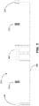
- FIG. 2 An example of a single-ended clock distribution circuit 200 is shown in the cross-sectional view of FIG. 2 .
- the clock lines 202 may be provided in the M11 layer of the integrated circuit, or other metal layers (e.g., M10).
- the two clock lines 202 run alongside each other for a non-trivial distance on the integrated circuit.
- a spacer 204 extend from the first layer 206 (e.g., the M9 layer of an integrated circuit) and runs between the clock lines 202.
- the spacer 204 may provide some isolation between the clock lines 202.
- Side isolation 214 are provided on either side of the clock lines 202.
- each clock line 202 has a width of 0.5 ⁇ m, and is positioned at a height of 2.35 ⁇ m from the first layer 206 and at a lateral distance of 4.52 ⁇ m from the spacer 204; the spacer has a width of 3.6 ⁇ m.
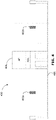
- FIG. 4 is a cross-sectional view of another single-ended clock distribution circuit 400, similar to that of FIG. 2 , but with the addition of a shield structure, in this case a shield wall 404 extending from the first layer 406.
- a shield structure in this case a shield wall 404 extending from the first layer 406.
- Two single-ended clock lines 402a, 402b (generally, clock line 402) run alongside each other for a distance.
- the shield wall 404 runs between the two clock lines 402, for at least a portion of the distance.
- Each clock line 402 carries a respective clock signal at respective different frequencies.
- the shield wall 404 may extend from the first layer 406 (e.g., M9 layer of the integrated circuit) up to the redistribution via layer (RDL) and may further extend up to the topmost metal layer, for example extending up to the aluminum for bond pad (AP) layer of the integrated circuit.
- the shield wall 404 has a height of about 7.075 ⁇ m (measured from the first layer 406).
- the height of the shield wall 404 depends on the layers to which the shield wall 404 is extended. For example, extending the shield wall 404 to the AP layer may provide a high enough shield wall 404 for better isolation between the clock lines 402.
- the simulated electric field emitted by one clock line 402a is plotted in FIG. 5 .
- the dimensions for this simulation are the same as those in the simulation shown in FIG. 3 , but with the addition of the shield wall 404.
- FIG. 5 isolation between the clock lines 402 is improved compared to the situation seen in FIG. 3 , due to the addition of the shield wall 404. From simulations, it was found that the arrangement shown in FIG. 4 was able to achieve isolation of -66dB at 15GHz between the clock lines 402, similar to the case where differential clock lines are used (e.g., as shown in FIG. 1 ).
- openings in the shield wall 404 may have different sizes to accommodate the passing of other signals that may be routed across the clock lines. Opening in the shield wall 404 may reduce the isolation between the clock lines 402. This may still satisfy jitter requirements, for example for lower frequency (e.g., below 1GHz) clock signals where jitter requirements are not as tight. Jitter requirements may also be satisfied even for higher frequency (e.g., 10-15GHz) clock signals if there are few such openings in the shield wall 404. Similarly, jitter requirements may also be satisfied if the clock distribution span is relatively short.
- FIG. 6A is a perspective view of another example clock distribution circuit 600.
- FIG. 6B is a top view of the circuit 600.
- This circuit 600 is similar to the circuit 400 of FIG. 4 , but the shield structure includes a shield cage 608 in addition to a shield wall 604 (similar to the shield wall 404 described above with respect to FIG. 4 ).
- the two single-ended clock lines 602a, 602b (generally, clock line 602) run alongside each other for a distance.
- the shield cage 608 extends from the first layer 606 and surrounds both clock lines 602 for at least a portion of the distance. It should be noted that the shield cage 608 surrounds but does not completely enclose the clock lines 602. That is, there are one or more openings in the shield cage 608.
- the shield cage 608 includes openings in side walls 610 and openings in an upper wall 612 extending between the side walls 610.
- the side walls 610 may extend from the first layer 606 up to the AP layer (similar to the shield wall 604).
- openings in the upper wall 612 may be about 9.54 ⁇ m (width, +/- 20%) ⁇ 42 ⁇ m (length, +/- 20%).
- length is measured along the longitudinal axis (i.e., the axis of the clock lines 602)
- width is measured laterally (i.e., in the direction between clock lines 602
- height is measured in the remaining Cartesian direction.
- the upper wall 612 may extend between the side walls 610 and along the AP layer.
- the openings in the side walls 610 may be provided to allow routing of other lines across the clock lines 602.
- openings in the side walls 610 may be about 2.35 ⁇ m (height) ⁇ 3.39 ⁇ m (length, +/-10%). Where both side walls 610 have openings, the openings may be staggered between the side walls 610 (so that there is no direct line-of-sight through both side walls 610), for better isolation. There may be no openings in the side walls 610 in some examples.
- side walls 610 and an upper wall 612 are shown to form the shield cage 608, other geometries may be used for the shield cage 608.
- the shield cage 608 may be formed as a single wall curving over both clock lines 602.
- shield cage 608 Although greater isolation between the clock lines 602 may be achieved with a solid shield cage 608 (i.e., without any openings), this may result in the shield cage 608 having an unacceptably high capacitance.
- design of the shield cage 608 may involve a trade-off between isolation and capacitance. Appropriate simulations may be carried out to determine suitable dimensions and configurations of the shield cage 608 to meet at least one of isolation and capacitance requirements.
- FIG. 11 An example of a shield cage having no top openings is shown in the example circuit 1100 of FIG. 11 .
- This circuit 1100 is similar to the circuit 600 of FIGS. 6A and 6B .
- a shield cage 1108 and shield wall 1104 is provided about clock lines 1102a, 1102b (generally, clock line 1102).
- the upper wall 1112 of the shield cage 1108 is shown semi-transparent, to allow better visualization of the circuit 1100.
- the shield cage 1108 has no openings in the upper wall 1112, however openings are still present in the side walls 1110.
- the shield cage 1108 extends from the first layer 1106 and surrounds both clock lines 1102 for at least a portion of the distance.
- FIGS. 7A and 7B show a perspective view and top view, respectively, of another configuration for the shield cage 708.
- the shield cage 708 has smaller openings which make up a smaller percentage of the overall upper wall 712. This may be suitable where the shield cage 708 needs to compensate for a shield wall 704 having many openings (e.g., to accommodate many lines across the clock lines 702).
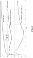
- FIG. 8 is a plot showing simulation results comparing the isolation of the clock lines in the example circuits of FIGS. 4 , 7A and 11 , over a range of frequencies.
- the shield cage 708 has side walls 710 spaced 4.52 ⁇ mto either side of the clock lines 702 and extending up to the AP layer.
- the upper wall 712 extends between the side walls 710 across the AP layer.
- Each opening in the upper wall 712 is a rectangle measuring 10 ⁇ m longitudinally (i.e., along the axis of the clock lines 702) and 9.54 ⁇ m laterally (both dimensions +/- 20%, for example), with a longitudinal spacing of 3 ⁇ mbetween openings. It was found that this configuration achieved an isolation of 100-84dB over a distance of about 120um, in the frequency range of interest (10-15GHz). This may be sufficient to achieve the desired isolation (e.g., meeting a requirement of at least 70dB isolation at a frequency of 15GHz).
- the circuit of FIG. 4 (simulated as having similar dimensions as described above but without a shield cage) is able to achieve an isolation of 66dB for a 120 ⁇ m circuit length in the frequency range 10-15GHz.
- the shield cage has no upper openings (simulated as having similar dimensions as described above but without openings in the upper wall of the shield cage) has isolation of about 125-120dB over the frequency range 10-15GHz.
- a shield cage without openings in the upper wall may exhibit unacceptably high capacitance, and not be practical to use. A higher capacitance would require a higher power consumption due to the buffers required to drive the clock signal in such high capacitance conditions.
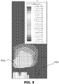
- the simulated electric field emitted by one clock line 702a is plotted in FIG. 9 , using the dimensions described above with respect to FIG. 8 .
- the second clock line 702b (shown by dotted lines) is completely isolated and experiences negligible electric field from the first clock line 702a.
- the shield cage 608 may have large openings (e.g., as shown in FIGS. 6A and 6B ) in one portion and have smaller openings (e.g., as shown in FIGS. 7A and 7B ) in another portion, to accommodate other requirements of the circuit design, for example to route control, data or power signals across the clock lines.
- the openings in the shield cage 608 may be regularly or irregularly shaped and may be regularly or irregularly spaced. Simulations may be carried out to determine appropriate configurations and dimensions of the openings.
- the first layer 206, 406, 606, 706 in the examples described above may also include openings.
- the first layer 706 below the shield cage 708 may have openings substantially the same as in the upper wall 712, but the openings in the first layer 706 may be offset from the openings in the upper wall 712 (so that there is no direct line-of-sight through both the upper wall 712 and the first layer 706), for better isolation.
- the present disclosure describes example shield cages having side walls and an upper wall, in some cases the first layer may conceptually be considered a bottom wall of the shield cage.
- the shield structure along the length of the clock lines may include any combination of shield wall and shield cage configurations (including one or the other).
- a combination of the configurations shown in any one of FIGS. 4 , 6 and 7A may be provided along the length of a pair of clock lines, to provide the desired isolation.
- a clock distribution circuit may have a portion along the length of the clock lines in which the shield structure has only the shield wall or only the shield cage, and another portion along the length in which the shield structure has both the shield wall and the shield cage.
- a clock distribution circuit may have a first portion along the length of the clock lines in which the shield structure has only the shield wall, a second portion along the length where the shield structure has only the shield cage, and a third portion along the length where the shield structure has both the shield wall and the shield cage.
- the shield structure may be desirable for the shield structure to include the shield wall as well as the shield cage (including side walls and upper wall) for as much of the clock distribution circuit as possible, to reduce crosstalk between clock lines.
- the shield structure may be varied along the clock distribution circuit to accommodate for circuit design requirements, such as to accommodate the presence and routing of other lines on the integrated circuit.
- the dimensions and configurations of either or both of the shield wall and shield cage may vary along the length of the clock lines.
- the shield cage may have larger openings in a first portion along the length of the clock lines and smaller openings in another portion (e.g., when there are more openings in the shield wall).
- FIG. 10 is a flowchart illustrating an example method 1000 for fabricating a clock distribution circuit including shield cage, for example the example circuits 600, 700 shown in FIGS. 6A to 7B .
- the circuits disclosed herein may be manufactured using any suitable chip manufacturing process, for example according to the Taiwan Semiconductor Manufacture Company (TSMC) N16FF+ process, or any other process applicable for chips including for 7nm, 16nm, 28nm and 65nm technologies.
- TSMC Taiwan Semiconductor Manufacture Company
- a portion of the shield wall is formed, extending from the first layer.
- the wall portion may be formed by deposition onto the first layer, or by etching away portions of the first layer.
- clock lines for different clock signals are formed, on either side of the wall portion. Any suitable deposition method may be used to form the clock lines.
- the wall portion may be extended to complete the shield wall.
- the side walls of the shield cage are also formed, extending from the first layer. This may be carried out as high layers of the integrated circuit is fabricated, for example using selective deposition or etching of subsequent metal layers.
- the shield cage is formed over the clock lines, extending between the side walls. This may be carried out during fabrication of the topmost metal layer (e.g., AP layer).
- the shield cage may be formed with appropriate openings in the upper wall of the shield cage, as described above, for example using suitable deposition or etching processes.
- a connection may be made to connect the first layer to a power supply, for example the ground of a power supply. This may result in the first layer serving as a ground layer (e.g., an AC ground layer).
- a power supply for example the ground of a power supply.
- the first layer serving as a ground layer (e.g., an AC ground layer).
- a single-ended clock distribution circuit is described that may enable the clock distribution span to be increased, compared with conventional approaches, for specified jitter limits.
- Example shielding configurations are described, which may help to reduce crosstalk between clocks and therefore reduce the associated clocking jitter.
- examples disclosed herein have been found to enable doubling of the clock distribution span and remain within specified jitter limits for high frequency applications.
- Examples disclosed herein may enable control of crosstalk as a tradeoff with line capacitance (which is viewed as a load by the line driver).
- line capacitance which is viewed as a load by the line driver.
- Examples disclosed herein may be suitable for use in any of high speed ADCs, long reach serializer/deserializers and short reach serializer/deserializers.
- the examples disclosed herein provide single-ended clock distribution, which may decrease the distribution power and area required, compared to differential clock distribution circuits.
- the shielding described herein, in the context of single-ended clock signals may also be suitable for shielding of differential clock signals.
- the shield wall may run between two pairs of differential clock lines.
- the shield cage may surround two pairs of differential clock lines.
- the example circuits may be adapted for more clock lines running side-by-side.
- examples described herein may also be adapted for clock distribution circuits having a single clock line (e.g., a single single-ended clock line or a single pair clock lines for a differential clock signal).
- a shield cage e.g., as described in the examples above
- This may serve to shield the single clock line from external interference (e.g., from other signals on the chip).
- the present disclosure may be useful to provide shielding even where crosstalk between parallel clock lines is not a concern.
- the present disclosure is described, at least in part, in terms of methods, a person of ordinary skill in the art will understand that the present disclosure is also directed to the various components for performing at least some of the aspects and features of the described methods, be it by way of hardware components, software or any combination of the two. Accordingly, the technical solution of the present disclosure may be embodied in the form of a software product.
- a suitable software product may be stored in a pre-recorded storage device or other similar non-volatile or non-transitory computer readable medium, including DVDs, CD-ROMs, USB flash disk, a removable hard disk, or other storage media, for example.
- the software product includes instructions tangibly stored thereon that enable a processing device (e.g., a personal computer, a server, or a network device) to execute examples of the methods disclosed herein.
Landscapes
- Engineering & Computer Science (AREA)
- Physics & Mathematics (AREA)
- Electromagnetism (AREA)
- Microelectronics & Electronic Packaging (AREA)
- Theoretical Computer Science (AREA)
- General Engineering & Computer Science (AREA)
- General Physics & Mathematics (AREA)
- Semiconductor Integrated Circuits (AREA)
- Design And Manufacture Of Integrated Circuits (AREA)
- Internal Circuitry In Semiconductor Integrated Circuit Devices (AREA)
Description
- The present disclosure relates to a shield structure used for a clock distribution circuit on a chip. In particular, the present disclosure relates to a shield structure used for a clock distribution circuit of single-ended clocks on a chip.
- Performance of serial interfaces relies on clocking quality, quantified by "clock jitter". As the speed of the interface increases, tolerance for clocking jitter decreases. For example, high frequency (e.g., 10-15 GHz) analog-to-digital conversion (ADC) circuits or serializer/deserializer circuits typically require sampling clocks to have jitter of less than a hundred femto seconds.
- In many cases, multiple clock lines carrying clock signals of different frequencies are routed alongside each other, and typically run alongside each other for a long distance (e.g., several millimeters). Crosstalk can occur between these clock lines, giving rise to mixing products that combine the frequencies of the different clock signals. Mixing products, once introduced, may be propagated and multiplied along the clock distribution circuit, for example due to active circuitry. This crosstalk thus introduces undesirable jitter in the clock signals and limits the critical clock distribution specification, which is the maximum span of quality clock routing within a chip.
- Although differential clock signals have been attempted to mitigate such crosstalk, use of differential clock signals requires increased power consumption and occupies greater area on a chip.
- In the prior art,
EP 1 187 206 A1 discloses an integrated circuit comprising a first layer, a first clock line for carrying a first clock signal, a second clock line for carrying a second clock signal, the second clock line running alongside the first clock line for a distance and a shield wall extending from the first layer, the shield wall running between the first and second clock lines for at least a portion of the distance. - Further,
EP 1688 996 A2 refers to a method of providing shield interconnection, the method shielding an interconnection pattern to be shielded with shield interconnection patterns for shielding on the substrate of a semiconductor integrated device. The method includes the steps of disposing multiple interconnection layers having the corresponding shield interconnection patterns formed therein, so that the interconnection layers surround the interconnection pattern to be shielded; setting different potentials for at least a first one of the shield interconnection patterns formed in a first one of the interconnection layers and a second one of the shield interconnection patterns formed in a second one of the interconnection layers; and shielding the interconnection pattern to be shielded with the first one and the second one of the shield interconnection patterns - The invention is defined and limited by the scope of the appended claims
- Reference will now be made, by way of example, to the accompanying drawings which show example embodiments of the present application, and in which:
-
FIG. 1 is a perspective view of an example prior art circuit for distribution of differential clock signals; -
FIG. 2 shows a cross-sectional view of an example not according to the invention circuit for distribution of single-ended clock signals; -
FIG. 3 is a plot showing a simulated electric field produced by one of the clock lines inFIG. 2 ; -
FIG. 4 shows a cross-sectional view of an example circuit not according to the invention for distribution of single-ended clock signals, including a shield wall; -
FIG. 5 is a plot showing a simulated electric field produced by one of the clock lines inFIG. 4 ; -
FIGS. 6A and6B show an example circuit for distribution of singled-ended clock signals, including an example shield cage; -
FIGS. 7A and7B show an example circuit for distribution of singled-ended clock signals, including another example shield cage; -
FIG. 8 is a plot of simulation results comparing isolation between clock lines in the example circuits ofFIGS. 4 ,7A and11 ; -
FIG. 9 is a plot showing a simulated electric field produced by one of the clock lines inFIG. 7A ; -
FIG. 10 is a flowchart illustrating an example method for fabricating the example circuits disclosed herein; and -
FIG. 11 shows an example circuit not according to the invention having a shield cage without openings. - Similar reference numerals may have been used in different figures to denote similar components.
-
FIG. 1 shows an example conventional differentialclock distribution circuit 100. A differential clock signal is carried by a pair of clock lines. In this example, one pair ofclock lines 102a carries a clock signal at a first frequency f0 and a second pair ofclock lines 102b carries another clock signal at a different second frequency f1. Theclock lines ground isolation 104 extends from thefirst layer 106 and surrounds each pair of clock lines 102 from three sides. In the present disclosure, a "first layer" may generally be any layer on which the clock distribution circuit is provided. The first layer may be connected to a power supply, for example the ground of a power supply. In some examples, the first layer may be a ground layer, for example an AC ground layer. An AC ground may serve to provide a near zero resistance path to ground, at the lowest frequency of interest. Thus, the first layer need not be connected to a direct current (DC) ground. Theisolation 104 may be connected to ground or to a low impedance supply, for example via thefirst layer 106. A differential signal approach may allow for the two pairs of clock lines 102, carrying different frequency clock signals, to run alongside each other with limited crosstalk. However, this approach requires twice as much space as a single-ended approach. Further, more active drivers are required to drive the clock lines 102, two for eachpair - Using single-ended clock distribution circuit may enable a decrease (e.g., about 20% decrease) in the area occupied by the clock distribution circuit, and a decrease (e.g., about 50% decrease) in power consumption, compared to a differential clock distribution circuit.
- An example of a single-ended
clock distribution circuit 200 is shown in the cross-sectional view ofFIG. 2 . In thisexample circuit 200, twoclock lines spacer 204 extend from the first layer 206 (e.g., the M9 layer of an integrated circuit) and runs between the clock lines 202. Thespacer 204 may provide some isolation between the clock lines 202.Side isolation 214 are provided on either side of the clock lines 202. - However, as seen in the simulated electric field plotted in
FIG. 3 , isolation between the clock lines 202 is poor. In the simulation shown, each clock line 202 has a width of 0.5µm, and is positioned at a height of 2.35µm from thefirst layer 206 and at a lateral distance of 4.52µm from thespacer 204; the spacer has a width of 3.6µm. -
FIG. 4 is a cross-sectional view of another single-endedclock distribution circuit 400, similar to that ofFIG. 2 , but with the addition of a shield structure, in this case ashield wall 404 extending from thefirst layer 406. Two single-ended clock lines shield wall 404 runs between the two clock lines 402, for at least a portion of the distance. Each clock line 402 carries a respective clock signal at respective different frequencies. In this example, theshield wall 404 may extend from the first layer 406 (e.g., M9 layer of the integrated circuit) up to the redistribution via layer (RDL) and may further extend up to the topmost metal layer, for example extending up to the aluminum for bond pad (AP) layer of the integrated circuit. In this example, theshield wall 404 has a height of about 7.075µm (measured from the first layer 406). Generally, the height of theshield wall 404 depends on the layers to which theshield wall 404 is extended. For example, extending theshield wall 404 to the AP layer may provide a highenough shield wall 404 for better isolation between the clock lines 402. - The simulated electric field emitted by one
clock line 402a is plotted inFIG. 5 . The dimensions for this simulation are the same as those in the simulation shown inFIG. 3 , but with the addition of theshield wall 404. As can be seen inFIG. 5 , isolation between the clock lines 402 is improved compared to the situation seen inFIG. 3 , due to the addition of theshield wall 404. From simulations, it was found that the arrangement shown inFIG. 4 was able to achieve isolation of -66dB at 15GHz between the clock lines 402, similar to the case where differential clock lines are used (e.g., as shown inFIG. 1 ). - It should be noted that in some cases it may be necessary to provide openings in the
shield wall 404 to allow routing of at least one of other signals and power lines across the clock lines 402. The openings in theshield wall 404 may have different sizes to accommodate the passing of other signals that may be routed across the clock lines. Opening in theshield wall 404 may reduce the isolation between the clock lines 402. This may still satisfy jitter requirements, for example for lower frequency (e.g., below 1GHz) clock signals where jitter requirements are not as tight. Jitter requirements may also be satisfied even for higher frequency (e.g., 10-15GHz) clock signals if there are few such openings in theshield wall 404. Similarly, jitter requirements may also be satisfied if the clock distribution span is relatively short. -
FIG. 6A is a perspective view of another exampleclock distribution circuit 600.FIG. 6B is a top view of thecircuit 600. Thiscircuit 600 is similar to thecircuit 400 ofFIG. 4 , but the shield structure includes ashield cage 608 in addition to a shield wall 604 (similar to theshield wall 404 described above with respect toFIG. 4 ). The two single-endedclock lines shield cage 608 extends from thefirst layer 606 and surrounds both clock lines 602 for at least a portion of the distance. It should be noted that theshield cage 608 surrounds but does not completely enclose the clock lines 602. That is, there are one or more openings in theshield cage 608. - For example, the
shield cage 608 includes openings inside walls 610 and openings in anupper wall 612 extending between theside walls 610. Theside walls 610 may extend from thefirst layer 606 up to the AP layer (similar to the shield wall 604). In this example, openings in theupper wall 612 may be about 9.54µm (width, +/- 20%) × 42µm (length, +/- 20%). In the present disclosure, length is measured along the longitudinal axis (i.e., the axis of the clock lines 602), width is measured laterally (i.e., in the direction between clock lines 602, and height is measured in the remaining Cartesian direction. Theupper wall 612 may extend between theside walls 610 and along the AP layer. The openings in theside walls 610 may be provided to allow routing of other lines across the clock lines 602. For example, openings in theside walls 610 may be about 2.35µm (height) × 3.39µm (length, +/-10%). Where bothside walls 610 have openings, the openings may be staggered between the side walls 610 (so that there is no direct line-of-sight through both side walls 610), for better isolation. There may be no openings in theside walls 610 in some examples. Thoughside walls 610 and anupper wall 612 are shown to form theshield cage 608, other geometries may be used for theshield cage 608. For example, theshield cage 608 may be formed as a single wall curving over both clock lines 602. - Although greater isolation between the clock lines 602 may be achieved with a solid shield cage 608 (i.e., without any openings), this may result in the
shield cage 608 having an unacceptably high capacitance. Thus, design of theshield cage 608 may involve a trade-off between isolation and capacitance. Appropriate simulations may be carried out to determine suitable dimensions and configurations of theshield cage 608 to meet at least one of isolation and capacitance requirements. - An example of a shield cage having no top openings is shown in the
example circuit 1100 ofFIG. 11 . Thiscircuit 1100 is similar to thecircuit 600 ofFIGS. 6A and6B . Ashield cage 1108 andshield wall 1104 is provided aboutclock lines upper wall 1112 of theshield cage 1108 is shown semi-transparent, to allow better visualization of thecircuit 1100. Theshield cage 1108 has no openings in theupper wall 1112, however openings are still present in theside walls 1110. Theshield cage 1108 extends from thefirst layer 1106 and surrounds both clock lines 1102 for at least a portion of the distance. - For example,
FIGS. 7A and7B show a perspective view and top view, respectively, of another configuration for theshield cage 708. Compared to the example ofFIGS. 6A and6B , theshield cage 708 has smaller openings which make up a smaller percentage of the overallupper wall 712. This may be suitable where theshield cage 708 needs to compensate for ashield wall 704 having many openings (e.g., to accommodate many lines across the clock lines 702). -
FIG. 8 is a plot showing simulation results comparing the isolation of the clock lines in the example circuits ofFIGS. 4 ,7A and11 , over a range of frequencies. - In simulating the circuit of
FIGS. 7A and7B , theshield cage 708 hasside walls 710 spaced 4.52µmto either side of the clock lines 702 and extending up to the AP layer. Theupper wall 712 extends between theside walls 710 across the AP layer. Each opening in theupper wall 712 is a rectangle measuring 10µm longitudinally (i.e., along the axis of the clock lines 702) and 9.54µm laterally (both dimensions +/- 20%, for example), with a longitudinal spacing of 3µmbetween openings. It was found that this configuration achieved an isolation of 100-84dB over a distance of about 120um, in the frequency range of interest (10-15GHz). This may be sufficient to achieve the desired isolation (e.g., meeting a requirement of at least 70dB isolation at a frequency of 15GHz). - As shown in
FIG. 8 , the circuit ofFIG. 4 (simulated as having similar dimensions as described above but without a shield cage) is able to achieve an isolation of 66dB for a 120µm circuit length in the frequency range 10-15GHz. In the circuit ofFIG. 11 , where the shield cage has no upper openings (simulated as having similar dimensions as described above but without openings in the upper wall of the shield cage) has isolation of about 125-120dB over the frequency range 10-15GHz. However, as discussed above, in some specific implementations and semiconductor processes, a shield cage without openings in the upper wall may exhibit unacceptably high capacitance, and not be practical to use. A higher capacitance would require a higher power consumption due to the buffers required to drive the clock signal in such high capacitance conditions. - The simulated electric field emitted by one
clock line 702a is plotted inFIG. 9 , using the dimensions described above with respect toFIG. 8 . As can be seen inFIG. 9 , thesecond clock line 702b (shown by dotted lines) is completely isolated and experiences negligible electric field from thefirst clock line 702a. - In some examples, there may be one or more portions along the length of the clock lines 602 where the shield structure consists of only the
shield wall 604 without theshield cage 608, there may be one or more portions along the length of the clock lines 602 where the shield structure consists of only theshield cage 608 without the shield wall 604 (e.g., to accommodate routing of at least one of other signals and power lines across the clock lines 602), and there may be one or more portions along the length of the clock lines 602 where the shield structure includes both theshield wall 604 and theshield cage 608. Further, the configuration of theshield cage 608 may be varied along the length of the clock lines 602. For example, in a real integrated circuit implementation, along the distance travelled by the clock distribution circuit, theshield cage 608 may have large openings (e.g., as shown inFIGS. 6A and6B ) in one portion and have smaller openings (e.g., as shown inFIGS. 7A and7B ) in another portion, to accommodate other requirements of the circuit design, for example to route control, data or power signals across the clock lines. The openings in theshield cage 608 may be regularly or irregularly shaped and may be regularly or irregularly spaced. Simulations may be carried out to determine appropriate configurations and dimensions of the openings. - It should be noted that the
first layer first layer 706 below theshield cage 708 may have openings substantially the same as in theupper wall 712, but the openings in thefirst layer 706 may be offset from the openings in the upper wall 712 (so that there is no direct line-of-sight through both theupper wall 712 and the first layer 706), for better isolation. Although the present disclosure describes example shield cages having side walls and an upper wall, in some cases the first layer may conceptually be considered a bottom wall of the shield cage. - It should be noted that the shield structure along the length of the clock lines may include any combination of shield wall and shield cage configurations (including one or the other). For example, a combination of the configurations shown in any one of
FIGS. 4 ,6 and7A may be provided along the length of a pair of clock lines, to provide the desired isolation. For example, a clock distribution circuit may have a portion along the length of the clock lines in which the shield structure has only the shield wall or only the shield cage, and another portion along the length in which the shield structure has both the shield wall and the shield cage. In another example, a clock distribution circuit may have a first portion along the length of the clock lines in which the shield structure has only the shield wall, a second portion along the length where the shield structure has only the shield cage, and a third portion along the length where the shield structure has both the shield wall and the shield cage. Where possible, it may be desirable for the shield structure to include the shield wall as well as the shield cage (including side walls and upper wall) for as much of the clock distribution circuit as possible, to reduce crosstalk between clock lines. However, in real implementation, the shield structure may be varied along the clock distribution circuit to accommodate for circuit design requirements, such as to accommodate the presence and routing of other lines on the integrated circuit. - It should also be noted that the dimensions and configurations of either or both of the shield wall and shield cage may vary along the length of the clock lines. For example, the shield cage may have larger openings in a first portion along the length of the clock lines and smaller openings in another portion (e.g., when there are more openings in the shield wall).
-
FIG. 10 is a flowchart illustrating anexample method 1000 for fabricating a clock distribution circuit including shield cage, for example theexample circuits FIGS. 6A to 7B . Generally, the circuits disclosed herein may be manufactured using any suitable chip manufacturing process, for example according to the Taiwan Semiconductor Manufacture Company (TSMC) N16FF+ process, or any other process applicable for chips including for 7nm, 16nm, 28nm and 65nm technologies. - The following
example method 1000 is described as an example only and is not intended to be limiting or exhaustive. - At 1002, a portion of the shield wall is formed, extending from the first layer. The wall portion may be formed by deposition onto the first layer, or by etching away portions of the first layer.
- At 1004, clock lines for different clock signals are formed, on either side of the wall portion. Any suitable deposition method may be used to form the clock lines.
- At 1006, the wall portion may be extended to complete the shield wall. The side walls of the shield cage are also formed, extending from the first layer. This may be carried out as high layers of the integrated circuit is fabricated, for example using selective deposition or etching of subsequent metal layers.
- At 1008, the shield cage is formed over the clock lines, extending between the side walls. This may be carried out during fabrication of the topmost metal layer (e.g., AP layer). The shield cage may be formed with appropriate openings in the upper wall of the shield cage, as described above, for example using suitable deposition or etching processes.
- In some examples, a connection may be made to connect the first layer to a power supply, for example the ground of a power supply. This may result in the first layer serving as a ground layer (e.g., an AC ground layer).
- In examples disclosed herein, a single-ended clock distribution circuit is described that may enable the clock distribution span to be increased, compared with conventional approaches, for specified jitter limits. Example shielding configurations are described, which may help to reduce crosstalk between clocks and therefore reduce the associated clocking jitter. In simulations, examples disclosed herein have been found to enable doubling of the clock distribution span and remain within specified jitter limits for high frequency applications.
- Examples disclosed herein may enable control of crosstalk as a tradeoff with line capacitance (which is viewed as a load by the line driver). Generally, the larger the openings in the shield cage, the lower the capacitance but the higher the crosstalk. Accordingly, the driver load and the power consumption of the drivers may also be controlled as a tradeoff with crosstalk.
- Examples disclosed herein may be suitable for use in any of high speed ADCs, long reach serializer/deserializers and short reach serializer/deserializers.
- The examples disclosed herein provide single-ended clock distribution, which may decrease the distribution power and area required, compared to differential clock distribution circuits.
- It should be noted that the shielding described herein, in the context of single-ended clock signals, may also be suitable for shielding of differential clock signals. For example, the shield wall may run between two pairs of differential clock lines. As an additional example, The shield cage may surround two pairs of differential clock lines.
- Although the present disclosure describes circuits with two clock lines running side-by-side, the example circuits may be adapted for more clock lines running side-by-side. For example, there may be more than two single-ended clock lines running alongside each other, with shield walls between either or both of adjacent clock lines and a shield cage over the clock lines. In another example, there may be two or more pairs of different clock lines running alongside each other, with at least one of shield walls between adjacent pairs and a shield cage over the clock lines.
- It should also be noted that examples described herein may also be adapted for clock distribution circuits having a single clock line (e.g., a single single-ended clock line or a single pair clock lines for a differential clock signal). For example, a shield cage (e.g., as described in the examples above) may be provided to surround a single clock line. This may serve to shield the single clock line from external interference (e.g., from other signals on the chip). Thus, the present disclosure may be useful to provide shielding even where crosstalk between parallel clock lines is not a concern.
- Although the present disclosure describes methods and processes with steps in a certain order, one or more steps of the methods and processes may be omitted or altered as appropriate. One or more steps may take place in an order other than that in which they are described, as appropriate.
- Although the present disclosure is described, at least in part, in terms of methods, a person of ordinary skill in the art will understand that the present disclosure is also directed to the various components for performing at least some of the aspects and features of the described methods, be it by way of hardware components, software or any combination of the two. Accordingly, the technical solution of the present disclosure may be embodied in the form of a software product. A suitable software product may be stored in a pre-recorded storage device or other similar non-volatile or non-transitory computer readable medium, including DVDs, CD-ROMs, USB flash disk, a removable hard disk, or other storage media, for example. The software product includes instructions tangibly stored thereon that enable a processing device (e.g., a personal computer, a server, or a network device) to execute examples of the methods disclosed herein.
Claims (15)
- An integrated circuit (600) comprising:• a first layer (606);• a first clock line (602a) for carrying a first clock signal;• a second clock line (602b) for carrying a second clock signal, the second clock line (602b) running alongside the first clock line (602a) for a distance; and• a shield structure comprising a shield wall (604) extending from the first layer (606), the shield wall (604) running between the first and second clock lines (602a, 602b) for at least a portion of the distance,• wherein the shield structure further comprises a shield cage (608) extending from the first layer (606) and surrounding the first and second clock lines (602a, 602b) for at least a same or different portion of the distance, the shield cage (608) having defined therein a plurality of openings,• wherein the shield cage (608) comprises a first side wall and a second side wall forming together two side walls (610), the two side walls (610) extending from the first layer (606), each side wall (610) being positioned alongside a respective one of the first and second clock lines (602a, 602b), and comprises an upper wall (612) extending between the side walls (610) and over both, the first and second clock lines (602a, 602b), and wherein the plurality of openings is defined in at least the upper wall (612),• wherein the plurality of openings is further defined in the side walls (610), wherein openings among the plurality of openings are defined in the first side wall among the two side walls and further openings among the plurality of openings are defined in the second side wall among the two side walls, and the openings in the first side wall are staggered with respect to the further openings defined in the second side wall to avoid any direct line-of-sight through both, the first side wall and the second side wall.
- The integrated circuit of claim 1, wherein each opening defined in the side walls (610) has dimensions of about 2.35µm × 3.39µm.
- The integrated circuit of any one of claims 1 to 2, wherein each opening defined in the upper wall (612) has dimensions of about 9.54µm× 10µm.
- The integrated circuit of any one of claims 1 to 3, wherein each opening defined in the upper wall (612) has dimensions of about 9.54µm × 42µm.
- The integrated circuit of any one of claims 1 to 4, wherein the shield wall (604) has at least one opening defined therein.
- The integrated circuit of any one of claims 1 to 5, wherein:for a first portion of the distance, the shield structure includes only one of: the shield wall (604) or the shield cage (608); andfor a second portion of the distance, the shield structure includes both the shield wall (604) and the shield cage (608).
- The integrated circuit of any one of claims 1 to 6, wherein:for a first portion of the distance, the shield structure includes only the shield wall (604);for a second portion of the distance, the shield structure includes only the shield cage (608); andfor a third portion of the distance, the shield structure includes both the shield wall (604) and the shield cage (608).
- The integrated circuit of any one of claims 1 to 7, wherein the shield wall (604) extends from the first layer (606) to a topmost metal layer of the integrated circuit (600).
- The integrated circuit of any one of claims 7 and 8, wherein the shield cage (608) extends across the topmost metal layer, over the first and second clock lines (602a, 602b).
- The integrated circuit of any one of claims 1 to 9, wherein the first layer (606) has defined therein another plurality of openings.
- The integrated circuit of any one of claims 1 to 10, wherein the first clock signal is carried by a first pair of clock lines (602a), the second clock signal is carried by a second pair of clock lines (602b) running alongside the first pair, and the shield wall (604) runs between the first and second pairs of clock lines (602a, 602b).
- The integrated circuit of any one of claims 1 to 11, further comprising a third clock line carrying a third clock signal and a fourth clock line carrying a fourth clock signal, the third and fourth clock lines running alongside the first and second clock lines (602a, 602b) for at least the distance, wherein the shield structure comprises a plurality of shield walls (604), each shield wall (604) running between respective adjacent pairs of clock lines for at least a respective portion of the distance, and wherein the shield cages surrounds the first, second, third and fourth clock lines for at least the same or different portion of the distance.
- The integrated circuit of any one of claims 1 to 12, wherein the first layer (606) is connected to a power supply.
- The integrated circuit of any one of claims 1 to 13, wherein the first layer (606) is connected to a ground of a power supply.
- The integrated circuit of any one of claims 1 to 14 wherein the first layer (606) is an AC ground layer.
Priority Applications (1)
| Application Number | Priority Date | Filing Date | Title |
|---|---|---|---|
| EP22164613.6A EP4060732B1 (en) | 2017-03-31 | 2018-03-23 | Shield structure for a low crosstalk single ended clock distribution circuit |
Applications Claiming Priority (2)
| Application Number | Priority Date | Filing Date | Title |
|---|---|---|---|
| US15/476,463 US10939541B2 (en) | 2017-03-31 | 2017-03-31 | Shield structure for a low crosstalk single ended clock distribution circuit |
| PCT/CN2018/080277 WO2018177217A1 (en) | 2017-03-31 | 2018-03-23 | Shield structure for a low crosstalk single ended clock distribution circuit |
Related Child Applications (2)
| Application Number | Title | Priority Date | Filing Date |
|---|---|---|---|
| EP22164613.6A Division EP4060732B1 (en) | 2017-03-31 | 2018-03-23 | Shield structure for a low crosstalk single ended clock distribution circuit |
| EP22164613.6A Division-Into EP4060732B1 (en) | 2017-03-31 | 2018-03-23 | Shield structure for a low crosstalk single ended clock distribution circuit |
Publications (3)
| Publication Number | Publication Date |
|---|---|
| EP3586361A1 EP3586361A1 (en) | 2020-01-01 |
| EP3586361A4 EP3586361A4 (en) | 2020-04-08 |
| EP3586361B1 true EP3586361B1 (en) | 2022-05-25 |
Family
ID=63672632
Family Applications (2)
| Application Number | Title | Priority Date | Filing Date |
|---|---|---|---|
| EP22164613.6A Active EP4060732B1 (en) | 2017-03-31 | 2018-03-23 | Shield structure for a low crosstalk single ended clock distribution circuit |
| EP18777153.0A Active EP3586361B1 (en) | 2017-03-31 | 2018-03-23 | Shield structure for a low crosstalk single ended clock distribution circuit |
Family Applications Before (1)
| Application Number | Title | Priority Date | Filing Date |
|---|---|---|---|
| EP22164613.6A Active EP4060732B1 (en) | 2017-03-31 | 2018-03-23 | Shield structure for a low crosstalk single ended clock distribution circuit |
Country Status (4)
| Country | Link |
|---|---|
| US (1) | US10939541B2 (en) |
| EP (2) | EP4060732B1 (en) |
| CN (1) | CN110462824B (en) |
| WO (1) | WO2018177217A1 (en) |
Families Citing this family (2)
| Publication number | Priority date | Publication date | Assignee | Title |
|---|---|---|---|---|
| US10779402B1 (en) * | 2019-05-03 | 2020-09-15 | Intel Corporation | Noise sensitive trace 3D ground-shielding crosstalk mitigation |
| CN113014232A (en) * | 2021-02-23 | 2021-06-22 | 成都西瓴科技有限公司 | Low-jitter differential clock receiving circuit |
Citations (1)
| Publication number | Priority date | Publication date | Assignee | Title |
|---|---|---|---|---|
| EP1688996A2 (en) * | 2005-02-02 | 2006-08-09 | Ricoh Company, Ltd. | Semiconductor integrated device and method of providing shield interconnection therein |
Family Cites Families (48)
| Publication number | Priority date | Publication date | Assignee | Title |
|---|---|---|---|---|
| JPS5894202A (en) * | 1981-11-28 | 1983-06-04 | Mitsubishi Electric Corp | Microwave circuit |
| US5406235A (en) * | 1990-12-26 | 1995-04-11 | Tdk Corporation | High frequency device |
| US5381157A (en) * | 1991-05-02 | 1995-01-10 | Sumitomo Electric Industries, Ltd. | Monolithic microwave integrated circuit receiving device having a space between antenna element and substrate |
| JPH05136125A (en) | 1991-11-14 | 1993-06-01 | Hitachi Ltd | Clock wiring and semiconductor integrated circuit device having clock wiring |
| JPH07235741A (en) * | 1993-12-27 | 1995-09-05 | Ngk Spark Plug Co Ltd | Multilayer wiring board |
| US5994765A (en) | 1996-07-01 | 1999-11-30 | Sun Microsystems, Inc. | Clock distribution network with efficient shielding |
| US20020130739A1 (en) * | 1998-09-10 | 2002-09-19 | Cotton Martin A. | Embedded waveguide and embedded electromagnetic shielding |
| KR100308871B1 (en) * | 1998-12-28 | 2001-11-03 | 윤덕용 | coaxial type signal line and fabricating method thereof |
| JP2000269211A (en) * | 1999-03-15 | 2000-09-29 | Nec Corp | Semiconductor device |
| JP2001160663A (en) * | 1999-12-02 | 2001-06-12 | Nec Corp | Circuit board |
| US6400015B1 (en) * | 2000-03-31 | 2002-06-04 | Intel Corporation | Method of creating shielded structures to protect semiconductor devices |
| DE60140722D1 (en) | 2000-09-05 | 2010-01-21 | Nxp Bv | Integrated electromagnetic shielding device |
| US7292091B1 (en) * | 2000-10-11 | 2007-11-06 | Silicon Laboratories Inc. | Method and apparatus for reducing interference |
| US6731513B2 (en) * | 2002-03-15 | 2004-05-04 | Memx, Inc. | Shielded multi-conductor interconnect bus for MEMS |
| US6747340B2 (en) * | 2002-03-15 | 2004-06-08 | Memx, Inc. | Multi-level shielded multi-conductor interconnect bus for MEMS |
| US7049901B2 (en) * | 2002-12-10 | 2006-05-23 | Itt Manufacturing Enterprises Inc. | Parallel plate wave-guide structure in a layered medium for transmitting complementary signals |
| US6933599B2 (en) | 2003-10-27 | 2005-08-23 | Freescale Semiconductor, Inc. | Electromagnetic noise shielding in semiconductor packages using caged interconnect structures |
| DE102004014752B4 (en) * | 2004-03-25 | 2008-11-20 | Infineon Technologies Ag | Semiconductor device with coreless converter and half-bridge |
| US20060255434A1 (en) | 2005-05-12 | 2006-11-16 | Yinon Degani | Shielding noisy conductors in integrated passive devices |
| WO2007077623A1 (en) | 2006-01-04 | 2007-07-12 | Fujitsu Limited | Method for arranging shield line in semiconductor integrated circuit, semiconductor integrated circuit design device, and semiconductor integrated circuit design program |
| KR100731544B1 (en) * | 2006-04-13 | 2007-06-22 | 한국전자통신연구원 | Multilayer Coplanar Waveguide |
| WO2008068825A1 (en) * | 2006-12-01 | 2008-06-12 | Mitsubishi Electric Corporation | Coaxial line slot array antenna and its manufacturing method |
| JP2008218714A (en) * | 2007-03-05 | 2008-09-18 | Bridgestone Corp | Light-permeable electromagnetic wave shielding material and its production process, fine particle having extremely thin film of noble metal and its production process |
| JP2008288559A (en) | 2007-04-16 | 2008-11-27 | Panasonic Corp | Semiconductor integrated circuit and layout method of semiconductor integrated circuit |
| JP5216287B2 (en) | 2007-09-21 | 2013-06-19 | 株式会社日立製作所 | Semiconductor device |
| US7812694B2 (en) * | 2008-04-03 | 2010-10-12 | International Business Machines Corporation | Coplanar waveguide integrated circuits having arrays of shield conductors connected by bridging conductors |
| US8028406B2 (en) * | 2008-04-03 | 2011-10-04 | International Business Machines Corporation | Methods of fabricating coplanar waveguide structures |
| US8922293B2 (en) * | 2008-06-09 | 2014-12-30 | Taiwan Semiconductor Manufacturing Company, Ltd. | Microstrip lines with tunable characteristic impedance and wavelength |
| US8193878B2 (en) * | 2008-06-24 | 2012-06-05 | International Business Machines Corporation | Structure, structure and method for providing an on-chip variable delay transmission line with fixed characteristic impedance |
| US8279025B2 (en) * | 2008-12-09 | 2012-10-02 | Taiwan Semiconductor Manufacturing Company, Ltd. | Slow-wave coaxial transmission line having metal shield strips and dielectric strips with minimum dimensions |
| KR20100067817A (en) * | 2008-12-12 | 2010-06-22 | 삼성에스디아이 주식회사 | Optical filter and manufacturing method thereof |
| US8324979B2 (en) * | 2009-02-25 | 2012-12-04 | Taiwan Semiconductor Manufacturing Company, Ltd. | Coupled microstrip lines with ground planes having ground strip shields and ground conductor extensions |
| US8659371B2 (en) * | 2009-03-03 | 2014-02-25 | Bae Systems Information And Electronic Systems Integration Inc. | Three-dimensional matrix structure for defining a coaxial transmission line channel |
| US20100225425A1 (en) * | 2009-03-09 | 2010-09-09 | Taiwan Semiconductor Manufacturing Company, Ltd. | High performance coupled coplanar waveguides with slow-wave features |
| US8130059B2 (en) * | 2009-04-15 | 2012-03-06 | International Business Machines Corporation | On chip slow-wave structure, method of manufacture and design structure |
| US7999361B1 (en) * | 2010-02-19 | 2011-08-16 | Altera Corporation | Shielding structure for transmission lines |
| US8963286B2 (en) * | 2011-05-09 | 2015-02-24 | Marvell International Ltd. | Finger metal oxide metal capacitor structures |
| US20130002375A1 (en) | 2011-07-01 | 2013-01-03 | Mediatek Inc. | Transmission line structure with low crosstalk |
| US8988166B2 (en) * | 2011-10-02 | 2015-03-24 | International Business Machines Corporation | Structure and compact modeling of variable transmission lines |
| US8791008B2 (en) * | 2012-03-21 | 2014-07-29 | Stats Chippac, Ltd. | Semiconductor device and method of forming micro-vias partially through insulating material over bump interconnect conductive layer for stress relief |
| US8922291B2 (en) * | 2012-05-09 | 2014-12-30 | Intel IP Corporation | Differential transmission line shielded by two or more spaced groups of shields |
| US8789003B1 (en) * | 2013-04-22 | 2014-07-22 | International Business Machines Corporation | Millimeter wave phase shifters using tunable transmission lines |
| US9425603B2 (en) * | 2013-09-06 | 2016-08-23 | Easton Corporation | Bus plug apparatus using multiple interconnected enclosures |
| CA2913777A1 (en) * | 2014-12-15 | 2016-06-15 | University Of Windsor | Shielded rf transmission lines in low temperature co-fired ceramic constructs and method of making same |
| CN105226360B (en) * | 2015-08-24 | 2018-05-29 | 上海交通大学 | Substrate integrated coaxial waveguide interconnection array structure |
| US10804214B2 (en) * | 2016-06-27 | 2020-10-13 | Intel Corporation | Group III-N material conductive shield for high frequency metal interconnects |
| US10288825B2 (en) * | 2016-12-23 | 2019-05-14 | Hisense Broadband Multimedia Technologies Co., Ltd. | Optical module |
| KR101920870B1 (en) * | 2017-09-15 | 2018-11-21 | 한국과학기술연구원 | Non-contact measuring system amd method for optoelectronic properties of thin film |
-
2017
- 2017-03-31 US US15/476,463 patent/US10939541B2/en active Active
-
2018
- 2018-03-23 EP EP22164613.6A patent/EP4060732B1/en active Active
- 2018-03-23 WO PCT/CN2018/080277 patent/WO2018177217A1/en not_active Ceased
- 2018-03-23 EP EP18777153.0A patent/EP3586361B1/en active Active
- 2018-03-23 CN CN201880019132.5A patent/CN110462824B/en active Active
Patent Citations (1)
| Publication number | Priority date | Publication date | Assignee | Title |
|---|---|---|---|---|
| EP1688996A2 (en) * | 2005-02-02 | 2006-08-09 | Ricoh Company, Ltd. | Semiconductor integrated device and method of providing shield interconnection therein |
Also Published As
| Publication number | Publication date |
|---|---|
| CN110462824B (en) | 2021-05-14 |
| US10939541B2 (en) | 2021-03-02 |
| EP4060732A1 (en) | 2022-09-21 |
| WO2018177217A1 (en) | 2018-10-04 |
| EP3586361A1 (en) | 2020-01-01 |
| CN110462824A (en) | 2019-11-15 |
| EP3586361A4 (en) | 2020-04-08 |
| EP4060732B1 (en) | 2026-01-28 |
| US20180287618A1 (en) | 2018-10-04 |
Similar Documents
| Publication | Publication Date | Title |
|---|---|---|
| US20240105572A1 (en) | Ground via clustering for crosstalk mitigation | |
| JP3105885B2 (en) | VLSI circuit | |
| US7323785B2 (en) | Semiconductor device | |
| US9331026B1 (en) | Methods and apparatus for fabricating capacitor structures with a terminal shield | |
| CN102844864B (en) | For the shielding construction of transmission line | |
| EP4060732B1 (en) | Shield structure for a low crosstalk single ended clock distribution circuit | |
| US8203395B2 (en) | Wave guiding structures for crosstalk reduction | |
| EP1421620B1 (en) | Integrated circuit with signal lines and mesh layer | |
| US8390401B2 (en) | Coplanar waveguide | |
| US12057413B2 (en) | Package design scheme for enabling high-speed low-loss signaling and mitigation of manufacturing risk and cost | |
| JP5701806B2 (en) | EBG structure and semiconductor device | |
| EP2973692B1 (en) | Multi-layer core organic package substrate and its fabrication | |
| US8089004B2 (en) | Semiconductor device including wiring excellent in impedance matching, and method for designing the same | |
| JP2017050429A (en) | Signal wiring substrate | |
| JP2016081999A (en) | Circuit board and electronic device | |
| EP3125282B1 (en) | Surface-mount high-frequency circuit | |
| CN117558707B (en) | A three-dimensional metal isolation wiring structure and wiring method for preventing crosstalk | |
| EP1349212A2 (en) | Semiconductor integrated circuit with a shield wiring | |
| JP4919475B2 (en) | Manufacturing method of semiconductor integrated circuit | |
| JPS62203351A (en) | Interconnection structure of integrated circuit | |
| Ayers et al. | 112 Gbps SERDES Channel Design with 2.5 D Sub-Micron BEOL Interconnect | |
| US20010018988A1 (en) | Apparatus and method for reducing propagation delay in a conductor | |
| US20170092579A1 (en) | Multi-layer full dense mesh | |
| JP2009218526A (en) | Clock wiring structure, semiconductor device, and method for manufacturing semiconductor device | |
| CN102456669A (en) | Chip-grade electromagnetic interference shielding structure and manufacturing method thereof |
Legal Events
| Date | Code | Title | Description |
|---|---|---|---|
| STAA | Information on the status of an ep patent application or granted ep patent |
Free format text: STATUS: THE INTERNATIONAL PUBLICATION HAS BEEN MADE |
|
| PUAI | Public reference made under article 153(3) epc to a published international application that has entered the european phase |
Free format text: ORIGINAL CODE: 0009012 |
|
| STAA | Information on the status of an ep patent application or granted ep patent |
Free format text: STATUS: REQUEST FOR EXAMINATION WAS MADE |
|
| 17P | Request for examination filed |
Effective date: 20190924 |
|
| AK | Designated contracting states |
Kind code of ref document: A1 Designated state(s): AL AT BE BG CH CY CZ DE DK EE ES FI FR GB GR HR HU IE IS IT LI LT LU LV MC MK MT NL NO PL PT RO RS SE SI SK SM TR |
|
| AX | Request for extension of the european patent |
Extension state: BA ME |
|
| A4 | Supplementary search report drawn up and despatched |
Effective date: 20200311 |
|
| RIC1 | Information provided on ipc code assigned before grant |
Ipc: H01L 23/552 20060101AFI20200305BHEP Ipc: H01L 23/522 20060101ALI20200305BHEP Ipc: G06F 1/10 20060101ALI20200305BHEP |
|
| DAV | Request for validation of the european patent (deleted) | ||
| DAX | Request for extension of the european patent (deleted) | ||
| STAA | Information on the status of an ep patent application or granted ep patent |
Free format text: STATUS: EXAMINATION IS IN PROGRESS |
|
| 17Q | First examination report despatched |
Effective date: 20201116 |
|
| GRAP | Despatch of communication of intention to grant a patent |
Free format text: ORIGINAL CODE: EPIDOSNIGR1 |
|
| STAA | Information on the status of an ep patent application or granted ep patent |
Free format text: STATUS: GRANT OF PATENT IS INTENDED |
|
| INTG | Intention to grant announced |
Effective date: 20220103 |
|
| GRAS | Grant fee paid |
Free format text: ORIGINAL CODE: EPIDOSNIGR3 |
|
| GRAA | (expected) grant |
Free format text: ORIGINAL CODE: 0009210 |
|
| STAA | Information on the status of an ep patent application or granted ep patent |
Free format text: STATUS: THE PATENT HAS BEEN GRANTED |
|
| AK | Designated contracting states |
Kind code of ref document: B1 Designated state(s): AL AT BE BG CH CY CZ DE DK EE ES FI FR GB GR HR HU IE IS IT LI LT LU LV MC MK MT NL NO PL PT RO RS SE SI SK SM TR |
|
| REG | Reference to a national code |
Ref country code: GB Ref legal event code: FG4D |
|
| REG | Reference to a national code |
Ref country code: CH Ref legal event code: EP |
|
| REG | Reference to a national code |
Ref country code: AT Ref legal event code: REF Ref document number: 1494597 Country of ref document: AT Kind code of ref document: T Effective date: 20220615 Ref country code: DE Ref legal event code: R096 Ref document number: 602018036007 Country of ref document: DE |
|
| REG | Reference to a national code |
Ref country code: IE Ref legal event code: FG4D Ref country code: NL Ref legal event code: FP |
|
| REG | Reference to a national code |
Ref country code: LT Ref legal event code: MG9D |
|
| REG | Reference to a national code |
Ref country code: AT Ref legal event code: MK05 Ref document number: 1494597 Country of ref document: AT Kind code of ref document: T Effective date: 20220525 |
|
| PG25 | Lapsed in a contracting state [announced via postgrant information from national office to epo] |
Ref country code: SE Free format text: LAPSE BECAUSE OF FAILURE TO SUBMIT A TRANSLATION OF THE DESCRIPTION OR TO PAY THE FEE WITHIN THE PRESCRIBED TIME-LIMIT Effective date: 20220525 Ref country code: PT Free format text: LAPSE BECAUSE OF FAILURE TO SUBMIT A TRANSLATION OF THE DESCRIPTION OR TO PAY THE FEE WITHIN THE PRESCRIBED TIME-LIMIT Effective date: 20220926 Ref country code: NO Free format text: LAPSE BECAUSE OF FAILURE TO SUBMIT A TRANSLATION OF THE DESCRIPTION OR TO PAY THE FEE WITHIN THE PRESCRIBED TIME-LIMIT Effective date: 20220825 Ref country code: LT Free format text: LAPSE BECAUSE OF FAILURE TO SUBMIT A TRANSLATION OF THE DESCRIPTION OR TO PAY THE FEE WITHIN THE PRESCRIBED TIME-LIMIT Effective date: 20220525 Ref country code: HR Free format text: LAPSE BECAUSE OF FAILURE TO SUBMIT A TRANSLATION OF THE DESCRIPTION OR TO PAY THE FEE WITHIN THE PRESCRIBED TIME-LIMIT Effective date: 20220525 Ref country code: GR Free format text: LAPSE BECAUSE OF FAILURE TO SUBMIT A TRANSLATION OF THE DESCRIPTION OR TO PAY THE FEE WITHIN THE PRESCRIBED TIME-LIMIT Effective date: 20220826 Ref country code: FI Free format text: LAPSE BECAUSE OF FAILURE TO SUBMIT A TRANSLATION OF THE DESCRIPTION OR TO PAY THE FEE WITHIN THE PRESCRIBED TIME-LIMIT Effective date: 20220525 Ref country code: ES Free format text: LAPSE BECAUSE OF FAILURE TO SUBMIT A TRANSLATION OF THE DESCRIPTION OR TO PAY THE FEE WITHIN THE PRESCRIBED TIME-LIMIT Effective date: 20220525 Ref country code: BG Free format text: LAPSE BECAUSE OF FAILURE TO SUBMIT A TRANSLATION OF THE DESCRIPTION OR TO PAY THE FEE WITHIN THE PRESCRIBED TIME-LIMIT Effective date: 20220825 Ref country code: AT Free format text: LAPSE BECAUSE OF FAILURE TO SUBMIT A TRANSLATION OF THE DESCRIPTION OR TO PAY THE FEE WITHIN THE PRESCRIBED TIME-LIMIT Effective date: 20220525 |
|
| PG25 | Lapsed in a contracting state [announced via postgrant information from national office to epo] |
Ref country code: RS Free format text: LAPSE BECAUSE OF FAILURE TO SUBMIT A TRANSLATION OF THE DESCRIPTION OR TO PAY THE FEE WITHIN THE PRESCRIBED TIME-LIMIT Effective date: 20220525 Ref country code: PL Free format text: LAPSE BECAUSE OF FAILURE TO SUBMIT A TRANSLATION OF THE DESCRIPTION OR TO PAY THE FEE WITHIN THE PRESCRIBED TIME-LIMIT Effective date: 20220525 Ref country code: LV Free format text: LAPSE BECAUSE OF FAILURE TO SUBMIT A TRANSLATION OF THE DESCRIPTION OR TO PAY THE FEE WITHIN THE PRESCRIBED TIME-LIMIT Effective date: 20220525 Ref country code: IS Free format text: LAPSE BECAUSE OF FAILURE TO SUBMIT A TRANSLATION OF THE DESCRIPTION OR TO PAY THE FEE WITHIN THE PRESCRIBED TIME-LIMIT Effective date: 20220925 |
|
| PG25 | Lapsed in a contracting state [announced via postgrant information from national office to epo] |
Ref country code: SM Free format text: LAPSE BECAUSE OF FAILURE TO SUBMIT A TRANSLATION OF THE DESCRIPTION OR TO PAY THE FEE WITHIN THE PRESCRIBED TIME-LIMIT Effective date: 20220525 Ref country code: SK Free format text: LAPSE BECAUSE OF FAILURE TO SUBMIT A TRANSLATION OF THE DESCRIPTION OR TO PAY THE FEE WITHIN THE PRESCRIBED TIME-LIMIT Effective date: 20220525 Ref country code: RO Free format text: LAPSE BECAUSE OF FAILURE TO SUBMIT A TRANSLATION OF THE DESCRIPTION OR TO PAY THE FEE WITHIN THE PRESCRIBED TIME-LIMIT Effective date: 20220525 Ref country code: EE Free format text: LAPSE BECAUSE OF FAILURE TO SUBMIT A TRANSLATION OF THE DESCRIPTION OR TO PAY THE FEE WITHIN THE PRESCRIBED TIME-LIMIT Effective date: 20220525 Ref country code: DK Free format text: LAPSE BECAUSE OF FAILURE TO SUBMIT A TRANSLATION OF THE DESCRIPTION OR TO PAY THE FEE WITHIN THE PRESCRIBED TIME-LIMIT Effective date: 20220525 Ref country code: CZ Free format text: LAPSE BECAUSE OF FAILURE TO SUBMIT A TRANSLATION OF THE DESCRIPTION OR TO PAY THE FEE WITHIN THE PRESCRIBED TIME-LIMIT Effective date: 20220525 |
|
| REG | Reference to a national code |
Ref country code: DE Ref legal event code: R097 Ref document number: 602018036007 Country of ref document: DE |
|
| PG25 | Lapsed in a contracting state [announced via postgrant information from national office to epo] |
Ref country code: AL Free format text: LAPSE BECAUSE OF FAILURE TO SUBMIT A TRANSLATION OF THE DESCRIPTION OR TO PAY THE FEE WITHIN THE PRESCRIBED TIME-LIMIT Effective date: 20220525 |
|
| PLBE | No opposition filed within time limit |
Free format text: ORIGINAL CODE: 0009261 |
|
| STAA | Information on the status of an ep patent application or granted ep patent |
Free format text: STATUS: NO OPPOSITION FILED WITHIN TIME LIMIT |
|
| 26N | No opposition filed |
Effective date: 20230228 |
|
| PG25 | Lapsed in a contracting state [announced via postgrant information from national office to epo] |
Ref country code: SI Free format text: LAPSE BECAUSE OF FAILURE TO SUBMIT A TRANSLATION OF THE DESCRIPTION OR TO PAY THE FEE WITHIN THE PRESCRIBED TIME-LIMIT Effective date: 20220525 |
|
| PG25 | Lapsed in a contracting state [announced via postgrant information from national office to epo] |
Ref country code: MC Free format text: LAPSE BECAUSE OF FAILURE TO SUBMIT A TRANSLATION OF THE DESCRIPTION OR TO PAY THE FEE WITHIN THE PRESCRIBED TIME-LIMIT Effective date: 20220525 |
|
| REG | Reference to a national code |
Ref country code: CH Ref legal event code: PL |
|
| GBPC | Gb: european patent ceased through non-payment of renewal fee |
Effective date: 20230323 |
|
| REG | Reference to a national code |
Ref country code: BE Ref legal event code: MM Effective date: 20230331 |
|
| PG25 | Lapsed in a contracting state [announced via postgrant information from national office to epo] |
Ref country code: LU Free format text: LAPSE BECAUSE OF NON-PAYMENT OF DUE FEES Effective date: 20230323 |
|
| REG | Reference to a national code |
Ref country code: IE Ref legal event code: MM4A |
|
| PG25 | Lapsed in a contracting state [announced via postgrant information from national office to epo] |
Ref country code: GB Free format text: LAPSE BECAUSE OF NON-PAYMENT OF DUE FEES Effective date: 20230323 |
|
| PG25 | Lapsed in a contracting state [announced via postgrant information from national office to epo] |
Ref country code: LI Free format text: LAPSE BECAUSE OF NON-PAYMENT OF DUE FEES Effective date: 20230331 Ref country code: IE Free format text: LAPSE BECAUSE OF NON-PAYMENT OF DUE FEES Effective date: 20230323 Ref country code: GB Free format text: LAPSE BECAUSE OF NON-PAYMENT OF DUE FEES Effective date: 20230323 Ref country code: CH Free format text: LAPSE BECAUSE OF NON-PAYMENT OF DUE FEES Effective date: 20230331 |
|
| PG25 | Lapsed in a contracting state [announced via postgrant information from national office to epo] |
Ref country code: BE Free format text: LAPSE BECAUSE OF NON-PAYMENT OF DUE FEES Effective date: 20230331 |
|
| PG25 | Lapsed in a contracting state [announced via postgrant information from national office to epo] |
Ref country code: BG Free format text: LAPSE BECAUSE OF FAILURE TO SUBMIT A TRANSLATION OF THE DESCRIPTION OR TO PAY THE FEE WITHIN THE PRESCRIBED TIME-LIMIT Effective date: 20220525 |
|
| PG25 | Lapsed in a contracting state [announced via postgrant information from national office to epo] |
Ref country code: BG Free format text: LAPSE BECAUSE OF FAILURE TO SUBMIT A TRANSLATION OF THE DESCRIPTION OR TO PAY THE FEE WITHIN THE PRESCRIBED TIME-LIMIT Effective date: 20220525 |
|
| PG25 | Lapsed in a contracting state [announced via postgrant information from national office to epo] |
Ref country code: CY Free format text: LAPSE BECAUSE OF FAILURE TO SUBMIT A TRANSLATION OF THE DESCRIPTION OR TO PAY THE FEE WITHIN THE PRESCRIBED TIME-LIMIT; INVALID AB INITIO Effective date: 20180323 |
|
| PG25 | Lapsed in a contracting state [announced via postgrant information from national office to epo] |
Ref country code: HU Free format text: LAPSE BECAUSE OF FAILURE TO SUBMIT A TRANSLATION OF THE DESCRIPTION OR TO PAY THE FEE WITHIN THE PRESCRIBED TIME-LIMIT; INVALID AB INITIO Effective date: 20180323 |
|
| REG | Reference to a national code |
Ref country code: DE Ref legal event code: R079 Ref document number: 602018036007 Country of ref document: DE Free format text: PREVIOUS MAIN CLASS: H01L0023552000 Ipc: H10W0042200000 |
|
| PG25 | Lapsed in a contracting state [announced via postgrant information from national office to epo] |
Ref country code: TR Free format text: LAPSE BECAUSE OF FAILURE TO SUBMIT A TRANSLATION OF THE DESCRIPTION OR TO PAY THE FEE WITHIN THE PRESCRIBED TIME-LIMIT Effective date: 20220525 |
|
| PGFP | Annual fee paid to national office [announced via postgrant information from national office to epo] |
Ref country code: NL Payment date: 20260213 Year of fee payment: 9 |
|
| PGFP | Annual fee paid to national office [announced via postgrant information from national office to epo] |
Ref country code: DE Payment date: 20260204 Year of fee payment: 9 |
|
| PGFP | Annual fee paid to national office [announced via postgrant information from national office to epo] |
Ref country code: IT Payment date: 20260220 Year of fee payment: 9 |
|
| PGFP | Annual fee paid to national office [announced via postgrant information from national office to epo] |
Ref country code: FR Payment date: 20260209 Year of fee payment: 9 |