US10779402B1 - Noise sensitive trace 3D ground-shielding crosstalk mitigation - Google Patents
Noise sensitive trace 3D ground-shielding crosstalk mitigation Download PDFInfo
- Publication number
- US10779402B1 US10779402B1 US16/402,992 US201916402992A US10779402B1 US 10779402 B1 US10779402 B1 US 10779402B1 US 201916402992 A US201916402992 A US 201916402992A US 10779402 B1 US10779402 B1 US 10779402B1
- Authority
- US
- United States
- Prior art keywords
- gnd
- fence
- pair
- plane
- signal traces
- Prior art date
- Legal status (The legal status is an assumption and is not a legal conclusion. Google has not performed a legal analysis and makes no representation as to the accuracy of the status listed.)
- Active
Links
- 230000000116 mitigating effect Effects 0.000 title description 5
- 238000000034 method Methods 0.000 description 13
- 230000008878 coupling Effects 0.000 description 10
- 238000010168 coupling process Methods 0.000 description 10
- 238000005859 coupling reaction Methods 0.000 description 10
- 239000013078 crystal Substances 0.000 description 10
- 238000013461 design Methods 0.000 description 9
- 238000004519 manufacturing process Methods 0.000 description 9
- 230000006872 improvement Effects 0.000 description 8
- 238000004088 simulation Methods 0.000 description 8
- 230000006870 function Effects 0.000 description 5
- 238000002955 isolation Methods 0.000 description 5
- 239000002184 metal Substances 0.000 description 5
- 229910052751 metal Inorganic materials 0.000 description 5
- 230000008569 process Effects 0.000 description 5
- PXHVJJICTQNCMI-UHFFFAOYSA-N Nickel Chemical compound [Ni] PXHVJJICTQNCMI-UHFFFAOYSA-N 0.000 description 4
- 239000000463 material Substances 0.000 description 4
- 238000007747 plating Methods 0.000 description 4
- 239000004065 semiconductor Substances 0.000 description 4
- 230000008901 benefit Effects 0.000 description 3
- 238000004891 communication Methods 0.000 description 3
- 239000004020 conductor Substances 0.000 description 3
- 230000005684 electric field Effects 0.000 description 3
- 238000005516 engineering process Methods 0.000 description 2
- PCHJSUWPFVWCPO-UHFFFAOYSA-N gold Chemical compound [Au] PCHJSUWPFVWCPO-UHFFFAOYSA-N 0.000 description 2
- 239000010931 gold Substances 0.000 description 2
- 229910052737 gold Inorganic materials 0.000 description 2
- MSNOMDLPLDYDME-UHFFFAOYSA-N gold nickel Chemical compound [Ni].[Au] MSNOMDLPLDYDME-UHFFFAOYSA-N 0.000 description 2
- 238000007654 immersion Methods 0.000 description 2
- 230000036039 immunity Effects 0.000 description 2
- 229910052759 nickel Inorganic materials 0.000 description 2
- 230000005540 biological transmission Effects 0.000 description 1
- 230000001413 cellular effect Effects 0.000 description 1
- 230000008859 change Effects 0.000 description 1
- MPTQRFCYZCXJFQ-UHFFFAOYSA-L copper(II) chloride dihydrate Chemical compound O.O.[Cl-].[Cl-].[Cu+2] MPTQRFCYZCXJFQ-UHFFFAOYSA-L 0.000 description 1
- 238000013500 data storage Methods 0.000 description 1
- 230000000593 degrading effect Effects 0.000 description 1
- 238000010586 diagram Methods 0.000 description 1
- 230000000694 effects Effects 0.000 description 1
- 230000005672 electromagnetic field Effects 0.000 description 1
- 230000005284 excitation Effects 0.000 description 1
- 230000003993 interaction Effects 0.000 description 1
- 239000004973 liquid crystal related substance Substances 0.000 description 1
- 238000005259 measurement Methods 0.000 description 1
- 230000007246 mechanism Effects 0.000 description 1
- 230000002093 peripheral effect Effects 0.000 description 1
- 238000012545 processing Methods 0.000 description 1
- 229910000679 solder Inorganic materials 0.000 description 1
- 239000007787 solid Substances 0.000 description 1
- 230000001360 synchronised effect Effects 0.000 description 1
- 230000000007 visual effect Effects 0.000 description 1
Images


Classifications
-
- H—ELECTRICITY
- H05—ELECTRIC TECHNIQUES NOT OTHERWISE PROVIDED FOR
- H05K—PRINTED CIRCUITS; CASINGS OR CONSTRUCTIONAL DETAILS OF ELECTRIC APPARATUS; MANUFACTURE OF ASSEMBLAGES OF ELECTRICAL COMPONENTS
- H05K1/00—Printed circuits
- H05K1/02—Details
- H05K1/0284—Details of three-dimensional rigid printed circuit boards
-
- G—PHYSICS
- G06—COMPUTING; CALCULATING OR COUNTING
- G06F—ELECTRIC DIGITAL DATA PROCESSING
- G06F1/00—Details not covered by groups G06F3/00 - G06F13/00 and G06F21/00
- G06F1/04—Generating or distributing clock signals or signals derived directly therefrom
- G06F1/10—Distribution of clock signals, e.g. skew
-
- H—ELECTRICITY
- H01—ELECTRIC ELEMENTS
- H01L—SEMICONDUCTOR DEVICES NOT COVERED BY CLASS H10
- H01L23/00—Details of semiconductor or other solid state devices
- H01L23/48—Arrangements for conducting electric current to or from the solid state body in operation, e.g. leads, terminal arrangements ; Selection of materials therefor
- H01L23/488—Arrangements for conducting electric current to or from the solid state body in operation, e.g. leads, terminal arrangements ; Selection of materials therefor consisting of soldered or bonded constructions
- H01L23/498—Leads, i.e. metallisations or lead-frames on insulating substrates, e.g. chip carriers
- H01L23/49827—Via connections through the substrates, e.g. pins going through the substrate, coaxial cables
-
- H—ELECTRICITY
- H05—ELECTRIC TECHNIQUES NOT OTHERWISE PROVIDED FOR
- H05K—PRINTED CIRCUITS; CASINGS OR CONSTRUCTIONAL DETAILS OF ELECTRIC APPARATUS; MANUFACTURE OF ASSEMBLAGES OF ELECTRICAL COMPONENTS
- H05K1/00—Printed circuits
- H05K1/02—Details
- H05K1/0213—Electrical arrangements not otherwise provided for
- H05K1/0216—Reduction of cross-talk, noise or electromagnetic interference
- H05K1/0218—Reduction of cross-talk, noise or electromagnetic interference by printed shielding conductors, ground planes or power plane
- H05K1/0219—Printed shielding conductors for shielding around or between signal conductors, e.g. coplanar or coaxial printed shielding conductors
-
- H—ELECTRICITY
- H05—ELECTRIC TECHNIQUES NOT OTHERWISE PROVIDED FOR
- H05K—PRINTED CIRCUITS; CASINGS OR CONSTRUCTIONAL DETAILS OF ELECTRIC APPARATUS; MANUFACTURE OF ASSEMBLAGES OF ELECTRICAL COMPONENTS
- H05K2201/00—Indexing scheme relating to printed circuits covered by H05K1/00
- H05K2201/09—Shape and layout
- H05K2201/09209—Shape and layout details of conductors
- H05K2201/09654—Shape and layout details of conductors covering at least two types of conductors provided for in H05K2201/09218 - H05K2201/095
- H05K2201/09736—Varying thickness of a single conductor; Conductors in the same plane having different thicknesses
-
- H—ELECTRICITY
- H05—ELECTRIC TECHNIQUES NOT OTHERWISE PROVIDED FOR
- H05K—PRINTED CIRCUITS; CASINGS OR CONSTRUCTIONAL DETAILS OF ELECTRIC APPARATUS; MANUFACTURE OF ASSEMBLAGES OF ELECTRICAL COMPONENTS
- H05K3/00—Apparatus or processes for manufacturing printed circuits
- H05K3/22—Secondary treatment of printed circuits
- H05K3/24—Reinforcing the conductive pattern
- H05K3/244—Finish plating of conductors, especially of copper conductors, e.g. for pads or lands
Definitions
- the disclosure herein relates generally to structures to reduce crosstalk in small form factor circuitry and related methods therefor.
- FIG. 1 broadly illustrates a two dimensional (2D) ground (GND) trace in a noise-sensitive electronic network.
- FIG. 1A broadly illustrates a protruded three dimensional (3D) GND fence structure in a noise-sensitive electronic network, according to some embodiments.
- FIGS. 2 and 2A illustrate the 2D GND trace of FIG. 1 in additional detail, according to some embodiments.
- FIGS. 3 and 3A illustrate the 3D GND fence structure of FIG. 1A in additional detail, according to some embodiments.
- FIG. 4 is a graph showing decrease in Near End Crosstalk (NEXT) using a protruded 3D GND fence structure, according to some embodiments.
- NXT Near End Crosstalk
- FIG. 5 is a graph showing decrease in Far End Crosstalk (FEXT) using a protruded 3D GND fence structure, according to some embodiments.
- FEXT Far End Crosstalk
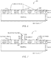
- FIG. 6 illustrates a standard printed circuit board (PCB) manufacturing process with a standard surface finish.
- PCB printed circuit board
- FIG. 7 illustrates additional process steps used to manufacture a printed circuit board with a protruded 3D GND fence, according to some embodiments.
- FIG. 8 is a flow chart that illustrates process steps useful in manufacturing a printed circuit board with a protruded 3D GND fence, according to some embodiments.
- FIG. 9 illustrates an example machine in accordance with some embodiments.
- a signal trace is generally understood to mean a conductive line configured to be connected, or in some embodiments already connected, as part of electronic circuitry. Sensitive nets from a crystal clock are usually routed in signal traces such as stripline, surrounded with ground to provide good referencing and noise shielding from other sources to reduce crosstalk.
- the disclosed subject matter relates to three dimensional (3D) ground (GND) fence-shielding to suppress electromagnetic (EM) crosstalk issues by using Z-height along GND traces as an improvement to prior crosstalk mitigation solutions.
- the Z-height can be targeted to be as much as the maximum distance available in the Z dimension.
- the Z-height is targeted to be no more than the height of the highest component on the board, so as not to add additional Z-height.
- FIG. 1 broadly illustrates a two dimensional (2D) GND trace in a sensitive noise-sensitive electronic network.
- the conventional 2D GND trace implementation seen generally at 101 is used to shield the signals.
- signal trace 103 is the aggressor trace (meaning the trace from which electromagnetic interference (EMI) originates) which may cause crosstalk to victim signal trace 105 (meaning the trace which experiences crosstalk from aggressor trace 103 , according to some embodiments).
- Crosstalk, or EMI is indicated symbolically by arrows, two of which are enumerated 111 , 113 .
- 2D GND trace 107 connected to ground by way of a number of vias in some embodiments, one of which is enumerated 109 , mitigates crosstalk.
- the vias are through-semiconductor vias.
- this 2D GND tracing has substantially the same Z-height as the neighboring signal traces, here 103 , 105 .
- Some, or in some embodiments, most, of the crosstalk is collected or attached by the 2D GND trace 107 , as indicated by arrows attracted to the 2D GND 107 .
- FIGS. 2 and 2A illustrate the 2D GND trace of FIG. 1 in additional detail, according to some embodiments.
- FIGS. 2 and 2A represent the concept of the conventional 2D GND trace implementation.
- FIG. 2 illustrates the 2D GND trace in perspective view 201 .
- 2D fence 207 is between aggressor trace 203 and victim trace 205 to reduce crosstalk between trace 203 and 205 .
- 2D GND trace 201 A is illustrated in side view, again between aggressor trace 203 A and victim trace 205 A, to reduce crosstalk between trace 203 A and trace 205 A.
- aggressor trace 203 A, 2D GND trace 207 A and victim trace 205 A are seen to be at the same level with respect to the top of the dielectric.
- 2D GND trace 207 A is illustrated as connected to ground by way of one or more vias in this embodiment.
- the via is illustrated as having a diameter less than the width of the 2D GND trace.
- the trace width and the via width could have the same geometry. Further, both trace width and via size will not appreciably impact the results achieved.
- FIG. 1A broadly illustrates a protruded three dimensional (3D) GND fence structure in a noise-sensitive electronic network, according to some embodiments.
- aggressor trace 104 may cause crosstalk to victim trace 106 .
- Crosstalk, or EMI is again indicated symbolically by the arrows.
- Protruded 3D GND trace 108 which extends above the level (or height) of traces 104 , 106 , is therefore considered 3D, because of using the indicated Z-height.
- the protruded 3D GND trace 108 of FIG. 1A is also above the level (or height) of 2D GND trace 107 of FIG. 1 .
- the protruded 3D GND fence 108 may therefore be referred to as 3D GND fence shielding.
- Protruded 3D GND fence shielding 108 is in some embodiments connected to the GND plane by way of vias such as 110 .
- Most, if not all, of the crosstalk such as arrow 112 is collected or attracted by the 3D GND fence 108 .
- Improved 3D GND fence-shielding has been found to suppress the EMI coupling by utilizing Z-height along the GND trace. With limitations in the X-Y area, the 3D GND “fence” structure can be constructed to reduce the noise coupling in the Z-direction.
- the thickness of the ground trace, or the Z-height is increased, assembling a “ground fence” structure to further block the EM field of the aggressor trace 104 from coupling to the victim trace 106 .
- FIGS. 3 and 3A illustrate the 3D GND fence structure of FIG. 1A in additional detail, according to some embodiments.
- FIG. 3 illustrates a 3D GND fence in perspective view 301 .
- 3D GND fence 307 is between aggressor trace 303 and victim trace 305 to reduce crosstalk between traces 303 and 305 .
- 3D GND fence 301 A is illustrated in side view, and illustrates the 3D GND fence 307 A between aggressor trace 303 A and victim trace 305 A, to reduce crosstalk between trace 303 A and trace 305 A.
- FIG. 3D GND fence 301 A is illustrated in side view, and illustrates the 3D GND fence 307 A between aggressor trace 303 A and victim trace 305 A, to reduce crosstalk between trace 303 A and trace 305 A.
- FIG. 3A the 3D GND fence 307 A protrudes above the level of aggressor trace 303 A and victim trace 305 A with respect to the top of the dielectric.
- the GND plane and the dielectric are illustrated in additional detail, with the 3D GND fence 307 A above the level of aggressor trace 303 A and victim trace 305 A, thus forming the fence illustrated symbolically in FIG. 1A .
- FIG. 3A also indicates that the 3D GND fence is connected to the GND plane by way of Via 310 A. In other words, FIG.
- FIG. 3 illustrates that the disclosed subject matter comprises a protruded 3D GND fence 307 on top of the conventional 2D GND trace, where material for the 3D GND fence may be added in the selected area during the selective plating process.
- FIG. 3A also illustrates the increased Z-height of the 3D GND fence in more detail. The rest of the design of FIGS. 2 and 2A remains substantially the same in FIGS. 3, 3A but for the 3D fence that uses increased Z-height.
- FIG. 4 is a graph showing decrease in Near End Crosstalk (NEXT) using a 3D GND fence structure, according to some embodiments.
- Simulation illustrates a comparison of the Near End Crosstalk (NEXT), the Far End Crosstalk (FEXT) and the Electric field (E-field) performance at the victim line.
- All the transmission line structures in the disclosed subject matter were solved for using HFSS 3D full-wave solver from 10 MHZ to 10 GHZ, with a 50 MHZ step size and solving frequency at 1 GHZ.
- excitation was induced on the aggressor trace, while the victim line was kept quiet, and the E-field was measured in Volts/meter. The results were probed at the victim line.
- FIG. 1 Near End Crosstalk
- Graph 402 indicates results using a 2D GND trace with a 30 ⁇ m thickness.
- the aggressor and the victim trace are each the same height as the 2D GND trace, namely 30 um.
- Graph 404 indicates results using a 3D GND fence at Z-height of 90 ⁇ m.
- Graph 406 indicates results using a 3D GND fence with a Z-height of 120 ⁇ m. With a 301 ⁇ m increase of the 2D GND trace thickness, an approximately 5 dB improvement is seen ( ⁇ 42.7947 dB versus ⁇ 37.8648 dB).
- FIG. 5 is a graph showing decrease in Far End Crosstalk (FEXT) using a 3D GND fence structure, according to some embodiments.
- Graph 502 indicates isolation results using a 2D GND trace.
- Graph 504 indicates results using a 3D GND fence at a Z-height of 90 ⁇ m.
- Graph 506 indicates results using a 3D GND fence at a Z-height of 120 ⁇ m.
- FEXT results show a similar performance trend as compared to the NEXT results.
- FIG. 5 shows that crosstalk improves by approximately 4 dB and approximately 5 dB, with an increased ground trace height of 30 ⁇ m and 120 ⁇ m, respectively.
- E-field Electric field
- 3D GND fence embodiments using the simulation setup described above for E-field measurements.
- Results comparing a conventional 2D GND trace to the disclosed 3D GND fence has shown that the EM field coupling from the aggressor trace to the victim trace is greatly reduced.
- the shielding effect was seen in simulation to be even better with further increased in Z-height.
- the simulation results again show that the protruding 3D GND will help suppress the resultant electric field coupling between the two conductors and, therefore, will ultimately enhance crosstalk immunity.
- Table 1 summarizes comparisons of observed results among a conventional 2D GND trace, a 3D GND fence with a first Z-height, and a 3D GND fence with an additional Z-height.
- PCB modeling was done on an implementation of the concept using ANSYSTM High Frequency Structure SimulatorTM (HFSS).
- HFSS High Frequency Structure Simulator
- the 2D ground trace 207 , 207 A of FIGS. 2 and 2A , respectively, having a 125 ⁇ m width and 30 ⁇ m height was placed in between a “victim” line indicated as Port 2 , Port 4 , of FIG. 2 and an “aggressor” line indicated as Port 1 , Port 3 in FIG. 2 .
- the dimensions of the aggressor and victim signal lines are the same.
- the bottom metal plane is assigned as GND.
- the ground trace 207 , 207 A was electrically shorted to the GND plane by placing two conductive metal rods at both ends of the trace in HFSS simulation port assignment. The actual board implementation would not have these connections.
- the protruding 3D GND fence 307 , 307 A of FIGS. 3 and 3A also having a 125 ⁇ m width and 90 ⁇ m height was placed in between a “victim” line or trace indicated as Port 6 , Port 8 , of FIG. 3 , and an “aggressor” line or trace indicated as Port 5 , Port 6 in FIG. 2 .
- the dimensions of the aggressor and victim signal lines are the same.
- the bottom metal plane is assigned as GND.
- the 3D GND fence 307 , 307 A was electrically shorted to the GND plane by placing two conductive metal rods at both ends of the 3D GND fence in simulation.
- FIG. 6 illustrates standard printed circuit board (PCB) manufacturing process 601 with a standard surface finish for a 2D GND trace implementations, with the dimensions representing dimensions of an embodiment.
- Prepreg is illustrated in this embodiment as 70 um in height, with the ground plane below the Prepreg.
- the aggressor trace and the victim trace are illustrated at 603 , 605 , respectively.
- the 2D GND trace is illustrated at 607 .
- Each is a copper trace with surface finish having a depth as may be appropriate for an embodiment.
- the disclosed 3D GND fence can be manufactured using standard PCB manufacturing technology, through additional process steps of selective plating during the surface finish process of FIG. 6 , according to some embodiments.
- the spacing between the traces 603 , 605 would be the spacing for a 3D GND fence that will be built on top of the 2D GND trace.
- the GND plane is as illustrated and 603 , 605 , 607 may be connected to the GND plane as in FIGS. 2, 2A , but the connections are not shown in FIG. 6 , for the purpose of clarity.
- FIG. 7 illustrates one or more additional process steps used to manufacture a printed circuit board with a 3D GND fence, according to some embodiments.
- FIG. 7 shows at 701 the one or more additional process step that can be used to manufacture the disclosed 3D GND fence in some embodiments.
- Prepreg is illustrated in this embodiment as 70 um in height, with the ground plane below the Prepreg.
- the 3D GND fence can be built on and contiguous with the 2D GND trace during the selective plating of the surface finish process using materials such as Electroless Nickel Immersion Gold (ENIG) or Hard Nickel Gold (HNG), which can be finished as were traces 703 , 705 .
- the materials may be applied to the finished 2D GND trace 708 to build the 3D fence with a targeted Z-height.
- the 3D GND fence will be exposed metal that protrudes above the solder resist layer.
- the GND plane is as illustrated and 703 , 705 , 707 may be connected to the GND plane as in FIGS. 3, 3A , but the connections are not shown in FIG. 7 , for the purpose of clarity. Since the structure is electrically GND, the protrusion does not represent a shorting concern if it comes into human contact.
- FIG. 8 is a flow chart 801 that illustrates process steps useful in manufacturing a printed circuit board with a 3D GND fence noise shielding, according to some embodiments.
- a standard PCB with 2D signal traces is implemented.
- a 2D grounded trace noise shield is implemented at a predetermined spacing between a pair of the 2D signal traces. Because a 3D GND fence will be implemented on the 2D GND tracing, the spacing distance would be the spacing distance used for a 3D GND fence as opposed to the greater spacing distance that would be used for a 2D grounded trace noise shield.
- a protruded 3D GND fence may be implemented on and contiguous with the 2D GND fence during the selective plating of the surface finish process for the PCB.
- the 3D GND fence may be implemented using materials such as Electroless Nickel Immersion Gold (ENIG) or Hard Nickel Gold (HNG) on the 2D GND trace, at a predetermined Z-height as is appropriate for the given embodiment.
- ENIG Electroless Nickel Immersion Gold
- HNG Hard Nickel Gold
- the surface of the protruded 3D GND fence may be finished according to usual semiconductor manufacturing practice.
- FIG. 9 illustrates a system level diagram, depicting an example of an electronic device (e.g., system) including one or more integrated circuits that implement 3D GND fence ground-shielding crosstalk mitigation as described in the present disclosure.
- FIG. 9 is included to show an example of a higher level device application for integrated circuits employing phase and length matching using slow wave structures.
- system 900 includes, but is not limited to, a desktop computer, a laptop computer, a netbook, a tablet, a notebook computer, a personal digital assistant (PDA), a server, a workstation, a cellular telephone, a mobile computing device, a smart phone, an Internet appliance or any other type of computing device.
- system 900 is a system on a chip (SOC) system.
- SOC system on a chip
- processor 910 has one or more processor cores 912 and 912 N, where 912 N represents the Nth processor core inside processor 910 where N is a positive integer.
- system 900 includes multiple processors including 910 and 905, where processor 905 has logic similar or identical to the logic of processor 910 .
- processing core 912 includes, but is not limited to, pre-fetch logic to fetch instructions, decode logic to decode the instructions, execution logic to execute instructions and the like.
- processor 910 has a cache memory 916 to cache instructions and/or data for system 900 . Cache memory 916 may be organized into a hierarchal structure including one or more levels of cache memory.
- processor 910 includes a memory controller 914 , which is operable to perform functions that enable the processor 910 to access and communicate with memory 930 that includes a volatile memory 932 and/or a non-volatile memory 934 .
- processor 910 is coupled with memory 930 and chipset 920 .
- Processor 910 may also be coupled to a wireless antenna 978 to communicate with any device configured to transmit and/or receive wireless signals.
- an interface for wireless antenna 978 operates in accordance with, but is not limited to, the IEEE 802.11 standard and its related family, Home Plug AV (HPAV), Ultra Wide Band (UWB), Bluetooth, WiMax, or any form of wireless communication protocol.
- volatile memory 932 includes, but is not limited to, Synchronous Dynamic Random Access Memory (SDRAM), Dynamic Random Access Memory (DRAM), RAMBUS Dynamic Random Access Memory (RDRAM), and/or any other type of random access memory device.
- Non-volatile memory 934 includes, but is not limited to, flash memory, phase change memory (PCM), read-only memory (ROM), electrically erasable programmable read-only memory (EEPROM), or any other type of non-volatile memory device.
- Memory 930 stores information and instructions to be executed by processor 910 .
- memory 930 may also store temporary variables or other intermediate information while processor 910 is executing instructions.
- chipset 920 connects with processor 910 via Point-to-Point (PtP or P-P) interfaces 917 and 922 .
- Chipset 920 enables processor 910 to connect to other elements in system 900 .
- interfaces 917 and 922 operate in accordance with a PtP communication protocol such as the Intel® QuickPath Interconnect (QPI) or the like. In other embodiments, a different interconnect may be used.
- PtP Point-to-Point
- QPI QuickPath Interconnect
- chipset 920 is operable to communicate with processor 910 , 905 N, display device 940 , and other devices, including a bus bridge 972 , a smart TV 976 , I/O devices 974 , nonvolatile memory 960 , a storage medium (such as one or more mass storage devices) 962 , a keyboard/mouse 964 , a network interface 966 , and various forms of consumer electronics 977 (such as a PDA, smart phone, tablet etc.), etc.
- chipset 920 couples with these devices through an interface 924 .
- Chipset 920 may also be coupled to a wireless antenna 978 to communicate with any device configured to transmit and/or receive wireless signals.
- Chipset 920 connects to display device 940 via interface 926 .
- Display 940 may be, for example, a liquid crystal display (LCD), a plasma display, cathode ray tube (CRT) display, or any other form of visual display device.
- processor 910 and chipset 920 are merged into a single SOC.
- chipset 920 connects to one or more buses 950 and 955 that interconnect various system elements, such as I/O devices 974 , nonvolatile memory 960 , storage medium 962 , a keyboard/mouse 964 , and network interface 966 .
- Buses 950 and 955 may be interconnected together via a bus bridge 972 .
- mass storage device 962 includes, but is not limited to, a solid state drive, a hard disk drive, a universal serial bus flash memory drive, or any other form of computer data storage medium.
- network interface 966 is implemented by any type of well-known network interface standard including, but not limited to, an Ethernet interface, a universal serial bus (USB) interface, a Peripheral Component Interconnect (PCI) Express interface, a wireless interface and/or any other suitable type of interface.
- the wireless interface operates in accordance with, but is not limited to, the IEEE 802.11 standard and its related family, Home Plug AV (HPAV), Ultra Wide Band (UWB), Bluetooth, WiMax, or any form of wireless communication protocol.
- modules shown in FIG. 9 are depicted as separate blocks within the system 900 , the functions performed by some of these blocks may be integrated within a single semiconductor circuit or may be implemented using two or more separate integrated circuits.
- cache memory 916 is depicted as a separate block within processor 910 , cache memory 916 (or selected embodiments of 916 ) can be incorporated into processor core 912 .
- Examples, as described herein, may include, or may operate on, logic or a number of components, modules, or mechanisms.
- Modules are tangible entities (e.g., hardware) capable of performing specified operations and may be configured or arranged in a certain manner.
- circuits may be arranged (e.g., internally or with respect to external entities such as other circuits) in a specified manner as a module.
- the whole or part of one or more computer systems e.g., a standalone, client or server computer system
- one or more hardware processors may be configured by firmware or software (e.g., instructions, an application portion, or an application) as a module that operates to perform specified operations.
- the software may reside on a machine readable medium.
- the software when executed by the underlying hardware of the module, causes the hardware to perform the specified operations.
- module is understood to encompass a tangible entity, be that an entity that is physically constructed, specifically configured (e.g., hardwired), or temporarily (e.g., transitorily) configured (e.g., programmed) to operate in a specified manner or to perform part or all of any operation described herein.
- each of the modules need not be instantiated at any one moment in time.
- the modules comprise a general-purpose hardware processor configured using software
- the general-purpose hardware processor may be configured as respective different modules at different times.
- Software may accordingly configure a hardware processor, for example, to constitute a particular module at one instance of time and to constitute a different module at a different instance of time.
- Example 1 is a printed circuit board (PCB), comprising: a dielectric plane; a ground plane parallel to and spaced apart from the dielectric plane; a pair of signal traces located parallel to each other on the dielectric plane; and a 3-dimensional (3D) grounded (GND) fence located on the dielectric plane between the pair of signal traces, and protruding perpendicularly from the dielectric plane to a height greater than the height of the pair of signal traces, wherein the 3D GND fence is configured to block electromagnetic interference (EMI) from a first of the pair of signal traces to a second of the pair of signal traces.
- EMI electromagnetic interference
- Example 2 the subject matter of Example 1 optionally includes wherein the pair of signal traces is configured to form part of a noise-sensitive clock circuit.
- Example 3 the subject matter of any one or more of Examples 1-2 optionally include D GND fence is electrically connected to the ground plane.
- Example 4 the subject matter of any one or more of Examples 1-3 optionally include D GND fence has a rectangular configuration parallel to the dielectric plane and a height dimension perpendicular to the dielectric plane.
- Example 5 the subject matter of any one or more of Examples 1-4 optionally include D GND fence is electrically connected to the ground plane by a via.
- Example 6 the subject matter of Example 5 optionally includes D GND fence is greater than a diameter of the circular cross section.
- Example 7 the subject matter of any one or more of Examples 1-6 optionally include D GND fence is located equidistant from each of the pair of signal traces.
- Example 8 the subject matter of any one or more of Examples 1-7 optionally include D GND fence perpendicular to the dielectric plane is no greater than the perpendicular dimension of the electronic component that has the greatest dimension perpendicular to the dielectric plane.
- Example 9 the subject matter of any one or more of Examples 1-8 optionally include D GND fence perpendicular to the dielectric plane is greater than the perpendicular dimension of the electronic component that has the greatest dimension perpendicular to the dielectric plane.
- Example 10 is a printed circuit board (PCB), comprising: a dielectric plane; a ground plane parallel to and spaced apart from the dielectric plane; a pair of signal traces located parallel to each other on the dielectric plane, the signal traces having a dimension perpendicular to the dielectric plane; a 2-dimensional (2D) grounded (GND) signal trace located on the dielectric plane between the pair of signal traces; and a 3-dimensional (3D) grounded (GND) fence located on and contiguous with the 2D GND signal trace, and protruding perpendicularly from the dielectric plane, wherein the 3D GND fence is configured to block electromagnetic interference (EMI) from a first of the pair of signal traces to a second of the pair of the signal traces.
- EMI electromagnetic interference
- Example 11 the subject matter of Example 10 optionally includes wherein the pair of signal traces is configured to form part of a noise-sensitive electronic circuit.
- Example 12 is a computer processor comprising: one or more processor cores; memory; and a memory controller, wherein the one or more processor cores, memory, and memory controller each includes: a printed circuit board (PCB) comprising: a dielectric plane; a ground plane parallel to and spaced from the dielectric plane; a pair of signal traces located parallel to each other on the dielectric plane; and a 3-dimensional (3D) grounded (GND) fence located between the pair of signal traces, and protruding perpendicularly from the dielectric plane, wherein the 3D GND fence is configured to block electromagnetic interference (EMI) from a first of the pair of signal traces and a second of the pair of the signal traces.
- PCB printed circuit board
- GND 3-dimensional
- EMI electromagnetic interference
- Example 13 the subject matter of Example 12 optionally includes wherein the pair of signal traces is configured to form part of a noise-sensitive electronic circuit.
- Example 14 the subject matter of any one or more of Examples 12-13 optionally include D GND fence is electrically connected to the ground plane.
- Example 15 the subject matter of any one or more of Examples 12-14 optionally include D GND fence has a rectangular configuration parallel to the dielectric plane and a height dimension perpendicular to the dielectric plane.
- Example 16 the subject matter of any one or more of Examples 12-15 optionally include D GND fence is electrically connected to the ground plane by a through-semiconductor via.
- Example 17 the subject matter of Example 16 optionally includes D GND fence is greater than a diameter of the circular cross section.
- Example 18 the subject matter of any one or more of Examples 12-17 optionally include D GND fence is located equidistant from each of the pair of signal traces.
- Example 19 the subject matter of any one or more of Examples 12-18 optionally include D GND fence perpendicular to the dielectric plane is no greater than the perpendicular dimension of the electronic component that has the greatest dimension perpendicular to the dielectric plane.
- Example 20 the subject matter of any one or more of Examples 12-19 optionally include the D GND fence perpendicular to the dielectric plane is greater than the perpendicular dimension of the electronic component that has the greatest dimension perpendicular to the dielectric plane.
- Example 21 the subject matter of any one or more of Examples 12-20 optionally include the pair of signal traces is configured to form part of a noise-sensitive clock circuit.
- Example 22 the subject matter can include, or can optionally be combined with any portion or combination of, any portions of any one or more of Examples 1 through 21 to include, subject matter that can include means for performing any one or more of the functions of Examples 1 through 21, or a machine-readable medium including instructions that, when performed by a machine, cause the machine to perform any one or more of the functions of Examples 1 through 21.
Abstract
A printed circuit board (PCB) includes a dielectric plane and a ground plane parallel to and spaced apart from the dielectric plane. The dielectric plane includes a pair of signal traces and a 3-dimensional (3D) grounded (GND) fence located between the pair of signal traces. The 3D GND fence is electrically connected to the ground plane, and protrudes perpendicularly from the dielectric plane. The 3D GND fence is located equidistant from each of the pair of signal traces, and the 3D GND fence is configured to block electromagnetic interference (EMI) from a first of the pair of signal traces to a second of the pair of the signal traces. The pair of signal traces is configured to form part of a noise-sensitive electronic circuit. The 3D GND fence may have a rectangular configuration.
Description
This application claims the benefit of priority to Malyasian Application Serial Number PI 2018702168, filed Jun. 4, 2018, which is incorporated herein by reference in its entirety.
The disclosure herein relates generally to structures to reduce crosstalk in small form factor circuitry and related methods therefor.
In some circuitry designs, particularly small form factor designs that include a crystal clock, signals are routed relatively near to each other and cause crosstalk noise coupling to the crystal network of the circuitry, degrading clock signals and, thus, the system performance. As printed circuit board area continues to shrink and bus speeds increase, crosstalk coupling will become more problematic and current solutions will not be efficient. Consequently, there is a need for improved mitigation of crosstalk in small form factor circuits.
In some circuit designs that include a crystal clock, signal coupling to the crystal network has been observed to result in increased the jitter on the crystal line. Such problems have been known to affect a display Phase-Locked Loop (PLL). This can ultimately cause issues such as screen flickering. Current solutions have been attempted in order to resolve such issues, but the observed resulting isolation was insufficient, even with large spacing applied for main routing with ground shielding. A signal trace is generally understood to mean a conductive line configured to be connected, or in some embodiments already connected, as part of electronic circuitry. Sensitive nets from a crystal clock are usually routed in signal traces such as stripline, surrounded with ground to provide good referencing and noise shielding from other sources to reduce crosstalk. However, the clock component in such circuits is usually placed on top of the PCB. Consequently, top layer microstrip routings are often unavoidable. This exposes the nets to greater crosstalk impact. Current solutions include a full 2D ground (GND) trace at the edge of the board to protect the crystal clock network. A minimum trace width is required that would mean a minimum amount of area needed for such implementations. Another current solution is to increase the spacing between the network and the signal lanes to minimize the interaction of the electromagnetic field with the adjacent conductors. Similarly, this would require trade-offs with the PCB real estate and signal performance. The disclosed subject matter relates to three dimensional (3D) ground (GND) fence-shielding to suppress electromagnetic (EM) crosstalk issues by using Z-height along GND traces as an improvement to prior crosstalk mitigation solutions. In some embodiments, the Z-height can be targeted to be as much as the maximum distance available in the Z dimension. In some embodiments the Z-height is targeted to be no more than the height of the highest component on the board, so as not to add additional Z-height.
Generally speaking, crosstalk is an undesired phenomena caused by the EM coupling between the PCB traces. FIG. 1 broadly illustrates a two dimensional (2D) GND trace in a sensitive noise-sensitive electronic network. For sensitive nets such as a crystal network, the conventional 2D GND trace implementation seen generally at 101 is used to shield the signals. For example, signal trace 103 is the aggressor trace (meaning the trace from which electromagnetic interference (EMI) originates) which may cause crosstalk to victim signal trace 105 (meaning the trace which experiences crosstalk from aggressor trace 103, according to some embodiments). Crosstalk, or EMI, is indicated symbolically by arrows, two of which are enumerated 111, 113. 2D GND trace 107, connected to ground by way of a number of vias in some embodiments, one of which is enumerated 109, mitigates crosstalk. In some embodiments the vias are through-semiconductor vias. Typically, this 2D GND tracing has substantially the same Z-height as the neighboring signal traces, here 103, 105. Some, or in some embodiments, most, of the crosstalk is collected or attached by the 2D GND trace 107, as indicated by arrows attracted to the 2D GND 107. However, some of the EM field from the aggressor trace 103 could still be coupled to the neighboring victim trace 105 via the Z-direction and can still cause crosstalk as indicated by arrows proceeding over 2D GND trace 107, one of which is enumerated 113. The impact increases as both the aggressor trace 103 and the victim trace 105 are placed closer to each other. The effectiveness of 2D GND trace isolation is typically up to −40 dB, which is generally insufficient to meet some of the current and expected stringent Phase-Locked Loop (PLL) jitter requirements and, thus, will directly impact some high frequency applications. Additionally, with the area constraint in Small Form Factor (SFF) design, the signal routing would be more congested. Consequently, there would be little or no additional room for area trade-offs. With current and future reduced PCB area, the 2D GND trace that surrounds the crystal network has been found to be insufficient to reduce the crosstalk and the EMI risk to the extent desired or needed.
Electric field (E-field) was also compared between 2D GND trace and 3D GND fence embodiments using the simulation setup described above for E-field measurements. Results comparing a conventional 2D GND trace to the disclosed 3D GND fence has shown that the EM field coupling from the aggressor trace to the victim trace is greatly reduced. The shielding effect was seen in simulation to be even better with further increased in Z-height. The simulation results again show that the protruding 3D GND will help suppress the resultant electric field coupling between the two conductors and, therefore, will ultimately enhance crosstalk immunity.
To obtain similar crosstalk improvement as that shown in FIGS. 4 and 5 , by using the conventional 2D ground fence routing, would entail using three times the spacing between the aggressor and victim traces compared to that used with the 3D GND fence. Therefore, the disclosed subject matter has been shown by simulation to be very effective in mitigating the crosstalk impact, without contributing significant extra X and Y area routing in PCB design. These improvements from 3D GND fence-shielding over earlier crosstalk solutions can be summarized in Table 1 below.
| TABLE I | |
| Improved noise | An improvement of 25% and 18.5% are achieved |
| immunity and | on both Far-End Crosstalk (FEXT) and Near-End |
| EMI shielding | Crosstalk (NEXT) respectively for the crystal |
| network. The ‘fence’ structure also offers better | |
| EMI shielding in the Z-direction to further minimize | |
| the crosstalk and noise coupling to adjacent | |
| conductors. | |
| Extended | The 3D GND fence would also provide similar |
| benefits to other | advantage to high speed bus applications such as |
| noise sensitive | High Speed Input/Output (HISO) and memory. |
| applications | The same principle could be applied ont he grounding |
| that shield high speed trace busses. | |
| Optimized SFF | Instead of 3x spacing required to meet same crosstalk |
| system design | improvement, by populating Z-height on the 2D |
| area | GND trace to form a 3D GND fence, it further |
| enhances the small form factor system design area. | |
| Feasible to SMT | With the growth of Surface Mount Technology |
| feature for | (SMT), the need of microstrip routing is still valid for |
| component pad | the component pad. |
Table 1, summarizes comparisons of observed results among a conventional 2D GND trace, a 3D GND fence with a first Z-height, and a 3D GND fence with an additional Z-height. PCB modeling was done on an implementation of the concept using ANSYS™ High Frequency Structure Simulator™ (HFSS).
The 2D ground trace 207, 207A of FIGS. 2 and 2A , respectively, having a 125 μm width and 30 μm height was placed in between a “victim” line indicated as Port 2, Port 4, of FIG. 2 and an “aggressor” line indicated as Port 1, Port3 in FIG. 2 . The dimensions of the aggressor and victim signal lines are the same. The bottom metal plane is assigned as GND. The ground trace 207, 207A was electrically shorted to the GND plane by placing two conductive metal rods at both ends of the trace in HFSS simulation port assignment. The actual board implementation would not have these connections.
Similarly to the 2D GND trace case, the protruding 3D GND fence 307, 307A of FIGS. 3 and 3A , also having a 125 μm width and 90 μm height was placed in between a “victim” line or trace indicated as Port 6, Port 8, of FIG. 3 , and an “aggressor” line or trace indicated as Port 5, Port 6 in FIG. 2 . The dimensions of the aggressor and victim signal lines are the same. The bottom metal plane is assigned as GND. The 3D GND fence 307, 307A was electrically shorted to the GND plane by placing two conductive metal rods at both ends of the 3D GND fence in simulation.
Aggregated isolation results are seen in Table 2, below. The second row of Table 2 indicates an example of the different spacing that is needed to achieve similar results as the 3D Ground Fence, with the conventional 2D Ground trace (2.25× and 3.5×).
| TABLE 2 | |||
| Trace | NEXT @ 1 | FEXT @ 1 | |
| Case | Height (μm) | GHz (dB) | GHz (dB) |
| |
30 | −37.86 | −36.38 |
| |
30 | 2.25x (−44.9) | 3.5x (−45.4) |
| with increased |
|||
| 3D Ground Fence | 90 | −42.79 | −40.33 |
| 3D Ground Fence with | 120 | −44.90 | −45.37 |
| additional height | |||
In one embodiment, processor 910 has one or more processor cores 912 and 912N, where 912N represents the Nth processor core inside processor 910 where N is a positive integer. In one embodiment, system 900 includes multiple processors including 910 and 905, where processor 905 has logic similar or identical to the logic of processor 910. In some embodiments, processing core 912 includes, but is not limited to, pre-fetch logic to fetch instructions, decode logic to decode the instructions, execution logic to execute instructions and the like. In some embodiments, processor 910 has a cache memory 916 to cache instructions and/or data for system 900. Cache memory 916 may be organized into a hierarchal structure including one or more levels of cache memory.
In some embodiments, processor 910 includes a memory controller 914, which is operable to perform functions that enable the processor 910 to access and communicate with memory 930 that includes a volatile memory 932 and/or a non-volatile memory 934. In some embodiments, processor 910 is coupled with memory 930 and chipset 920. Processor 910 may also be coupled to a wireless antenna 978 to communicate with any device configured to transmit and/or receive wireless signals. In one embodiment, an interface for wireless antenna 978 operates in accordance with, but is not limited to, the IEEE 802.11 standard and its related family, Home Plug AV (HPAV), Ultra Wide Band (UWB), Bluetooth, WiMax, or any form of wireless communication protocol.
In some embodiments, volatile memory 932 includes, but is not limited to, Synchronous Dynamic Random Access Memory (SDRAM), Dynamic Random Access Memory (DRAM), RAMBUS Dynamic Random Access Memory (RDRAM), and/or any other type of random access memory device. Non-volatile memory 934 includes, but is not limited to, flash memory, phase change memory (PCM), read-only memory (ROM), electrically erasable programmable read-only memory (EEPROM), or any other type of non-volatile memory device.
In some embodiments, chipset 920 is operable to communicate with processor 910, 905N, display device 940, and other devices, including a bus bridge 972, a smart TV 976, I/O devices 974, nonvolatile memory 960, a storage medium (such as one or more mass storage devices) 962, a keyboard/mouse 964, a network interface 966, and various forms of consumer electronics 977 (such as a PDA, smart phone, tablet etc.), etc. In one embodiment, chipset 920 couples with these devices through an interface 924. Chipset 920 may also be coupled to a wireless antenna 978 to communicate with any device configured to transmit and/or receive wireless signals.
In one embodiment, mass storage device 962 includes, but is not limited to, a solid state drive, a hard disk drive, a universal serial bus flash memory drive, or any other form of computer data storage medium. In one embodiment, network interface 966 is implemented by any type of well-known network interface standard including, but not limited to, an Ethernet interface, a universal serial bus (USB) interface, a Peripheral Component Interconnect (PCI) Express interface, a wireless interface and/or any other suitable type of interface. In one embodiment, the wireless interface operates in accordance with, but is not limited to, the IEEE 802.11 standard and its related family, Home Plug AV (HPAV), Ultra Wide Band (UWB), Bluetooth, WiMax, or any form of wireless communication protocol.
While the modules shown in FIG. 9 are depicted as separate blocks within the system 900, the functions performed by some of these blocks may be integrated within a single semiconductor circuit or may be implemented using two or more separate integrated circuits. For example, although cache memory 916 is depicted as a separate block within processor 910, cache memory 916 (or selected embodiments of 916) can be incorporated into processor core 912.
Examples, as described herein, may include, or may operate on, logic or a number of components, modules, or mechanisms. Modules are tangible entities (e.g., hardware) capable of performing specified operations and may be configured or arranged in a certain manner. In an example, circuits may be arranged (e.g., internally or with respect to external entities such as other circuits) in a specified manner as a module. In an example, the whole or part of one or more computer systems (e.g., a standalone, client or server computer system) or one or more hardware processors may be configured by firmware or software (e.g., instructions, an application portion, or an application) as a module that operates to perform specified operations. In an example, the software may reside on a machine readable medium. In an example, the software, when executed by the underlying hardware of the module, causes the hardware to perform the specified operations.
Accordingly, the term “module” is understood to encompass a tangible entity, be that an entity that is physically constructed, specifically configured (e.g., hardwired), or temporarily (e.g., transitorily) configured (e.g., programmed) to operate in a specified manner or to perform part or all of any operation described herein. Considering examples in which modules are temporarily configured, each of the modules need not be instantiated at any one moment in time. For example, where the modules comprise a general-purpose hardware processor configured using software, the general-purpose hardware processor may be configured as respective different modules at different times. Software may accordingly configure a hardware processor, for example, to constitute a particular module at one instance of time and to constitute a different module at a different instance of time.
Example 1 is a printed circuit board (PCB), comprising: a dielectric plane; a ground plane parallel to and spaced apart from the dielectric plane; a pair of signal traces located parallel to each other on the dielectric plane; and a 3-dimensional (3D) grounded (GND) fence located on the dielectric plane between the pair of signal traces, and protruding perpendicularly from the dielectric plane to a height greater than the height of the pair of signal traces, wherein the 3D GND fence is configured to block electromagnetic interference (EMI) from a first of the pair of signal traces to a second of the pair of signal traces.
In Example 2, the subject matter of Example 1 optionally includes wherein the pair of signal traces is configured to form part of a noise-sensitive clock circuit.
In Example 3, the subject matter of any one or more of Examples 1-2 optionally include D GND fence is electrically connected to the ground plane.
In Example 4, the subject matter of any one or more of Examples 1-3 optionally include D GND fence has a rectangular configuration parallel to the dielectric plane and a height dimension perpendicular to the dielectric plane.
In Example 5, the subject matter of any one or more of Examples 1-4 optionally include D GND fence is electrically connected to the ground plane by a via.
In Example 6, the subject matter of Example 5 optionally includes D GND fence is greater than a diameter of the circular cross section.
In Example 7, the subject matter of any one or more of Examples 1-6 optionally include D GND fence is located equidistant from each of the pair of signal traces.
In Example 8, the subject matter of any one or more of Examples 1-7 optionally include D GND fence perpendicular to the dielectric plane is no greater than the perpendicular dimension of the electronic component that has the greatest dimension perpendicular to the dielectric plane.
In Example 9, the subject matter of any one or more of Examples 1-8 optionally include D GND fence perpendicular to the dielectric plane is greater than the perpendicular dimension of the electronic component that has the greatest dimension perpendicular to the dielectric plane.
Example 10 is a printed circuit board (PCB), comprising: a dielectric plane; a ground plane parallel to and spaced apart from the dielectric plane; a pair of signal traces located parallel to each other on the dielectric plane, the signal traces having a dimension perpendicular to the dielectric plane; a 2-dimensional (2D) grounded (GND) signal trace located on the dielectric plane between the pair of signal traces; and a 3-dimensional (3D) grounded (GND) fence located on and contiguous with the 2D GND signal trace, and protruding perpendicularly from the dielectric plane, wherein the 3D GND fence is configured to block electromagnetic interference (EMI) from a first of the pair of signal traces to a second of the pair of the signal traces.
In Example 11, the subject matter of Example 10 optionally includes wherein the pair of signal traces is configured to form part of a noise-sensitive electronic circuit.
Example 12 is a computer processor comprising: one or more processor cores; memory; and a memory controller, wherein the one or more processor cores, memory, and memory controller each includes: a printed circuit board (PCB) comprising: a dielectric plane; a ground plane parallel to and spaced from the dielectric plane; a pair of signal traces located parallel to each other on the dielectric plane; and a 3-dimensional (3D) grounded (GND) fence located between the pair of signal traces, and protruding perpendicularly from the dielectric plane, wherein the 3D GND fence is configured to block electromagnetic interference (EMI) from a first of the pair of signal traces and a second of the pair of the signal traces.
In Example 13, the subject matter of Example 12 optionally includes wherein the pair of signal traces is configured to form part of a noise-sensitive electronic circuit.
In Example 14, the subject matter of any one or more of Examples 12-13 optionally include D GND fence is electrically connected to the ground plane.
In Example 15, the subject matter of any one or more of Examples 12-14 optionally include D GND fence has a rectangular configuration parallel to the dielectric plane and a height dimension perpendicular to the dielectric plane.
In Example 16, the subject matter of any one or more of Examples 12-15 optionally include D GND fence is electrically connected to the ground plane by a through-semiconductor via.
In Example 17, the subject matter of Example 16 optionally includes D GND fence is greater than a diameter of the circular cross section.
In Example 18, the subject matter of any one or more of Examples 12-17 optionally include D GND fence is located equidistant from each of the pair of signal traces.
In Example 19, the subject matter of any one or more of Examples 12-18 optionally include D GND fence perpendicular to the dielectric plane is no greater than the perpendicular dimension of the electronic component that has the greatest dimension perpendicular to the dielectric plane.
In Example 20, the subject matter of any one or more of Examples 12-19 optionally include the D GND fence perpendicular to the dielectric plane is greater than the perpendicular dimension of the electronic component that has the greatest dimension perpendicular to the dielectric plane.
In Example 21, the subject matter of any one or more of Examples 12-20 optionally include the pair of signal traces is configured to form part of a noise-sensitive clock circuit.
In Example 22, the subject matter can include, or can optionally be combined with any portion or combination of, any portions of any one or more of Examples 1 through 21 to include, subject matter that can include means for performing any one or more of the functions of Examples 1 through 21, or a machine-readable medium including instructions that, when performed by a machine, cause the machine to perform any one or more of the functions of Examples 1 through 21.
All features of the apparatuses described above (including optional features) may also be implemented with respect to the methods or processes described herein.
Claims (18)
1. A printed circuit board (PCB), comprising:
a dielectric plane;
a ground plane parallel to and spaced apart from the dielectric plane;
a pair of signal traces located parallel to each other on the dielectric plane;
a 3-dimensional (3D) grounded (GND) fence located on the dielectric plane between the pair of signal traces, and protruding perpendicularly from the dielectric plane to a height greater than the height of the pair of signal traces, wherein the 3D GND fence is configured to block electromagnetic interference (EMI) from a first of the pair of signal traces to a second of the pair of signal traces; and
a first via electrically connecting the 3D GND fence with the ground plane, wherein the first via has a first cross-sectional dimension; and
a second via coupled to the first of the pair of signal traces, wherein the second via has a second cross-sectional dimension, and the first cross-sectional dimension is less than the second cross-sectional dimension.
2. The PCB of claim 1 wherein the pair of signal traces is configured to form part of a noise-sensitive clock circuit.
3. The PCB of claim 1 wherein the 3D GND fence is electrically connected to the ground plane.
4. The PCB of claim 1 wherein the 3D GND fence has a rectangular configuration parallel to the dielectric plane and a height dimension perpendicular to the dielectric plane.
5. The PCB of claim 1 wherein the first via has a circular cross section and a width dimension of the 3D GND fence is greater than a diameter of the circular cross section.
6. The PCB of claim 1 wherein the 3D GND fence is located equidistant from each of the pair of signal traces.
7. The PCB of claim 1 wherein the dielectric plane includes a plurality of electronic components each with a dimension perpendicular to the dielectric plane, and the protrusion of the 3D GND fence perpendicular to the dielectric plane is no greater than the perpendicular dimension of the electronic component that has the greatest dimension perpendicular to the dielectric plane.
8. The PCB of claim 1 wherein the dielectric plane includes a plurality of electronic components each with a dimension perpendicular to the dielectric plane, and the protrusion of the 3D GND fence perpendicular to the dielectric plane is greater than the perpendicular dimension of the electronic component that has the greatest dimension perpendicular to the dielectric plane.
9. A printed circuit board (PCB), comprising:
a dielectric plane;
a ground plane parallel to and spaced apart from the dielectric plane;
a pair of signal traces located parallel to each other on the dielectric plane, the signal traces having a dimension perpendicular to the dielectric plane;
a 2-dimensional (2D) grounded (GND) signal trace located on the dielectric plane between the pair of signal traces; and
a 3-dimensional (3D) grounded (GND) fence located on and contiguous with the 2D GND signal trace, and protruding perpendicularly from the dielectric plane to a height greater than the height of the pair of signal traces and greater than the height of the 2D GND signal trace, wherein the 3D GND fence is configured to block electromagnetic interference (EMI) from a first of the pair of signal traces to a second of the pair of the signal traces;
a first via electrically connecting the 3D GND fence with the ground plane, wherein the first via has a first cross-sectional dimension; and
a second via coupled to a first of the pair of signal traces, wherein the second via has a second cross-sectional dimension, and the first cross-sectional dimension is less than the second cross-sectional dimension.
10. The PCB of claim 9 wherein the pair of signal traces is configured to form part of a noise-sensitive electronic circuit.
11. A computer processor comprising:
one or more processor cores;
memory; and
a memory controller, wherein the one or more processor cores, memory, and memory controller each includes:
a printed circuit board (PCB) comprising:
a dielectric plane;
a ground plane parallel to and spaced from the dielectric plane;
a pair of signal traces located parallel to each other on the dielectric plane;
a 3-dimensional (3D) grounded (GND) fence located between the pair of signal traces, and protruding perpendicularly from the dielectric plane, wherein the 3D GND fence is configured to block electromagnetic interference (EMI) from a first of the pair of signal traces and a second of the pair of the signal traces;
a first via electrically connecting the 3D GND fence with the ground plane, wherein the first via has a first cross-sectional dimension; and
a second via coupled to a first of the pair of signal traces, wherein the second via has a second cross-sectional dimension, and the first cross-sectional dimension is less than the second cross-sectional dimension.
12. The computer processor of claim 11 wherein the pair of signal traces is configured to form part of a noise-sensitive electronic circuit.
13. The computer processor of claim 11 wherein the PCB further comprises a ground plane parallel to and spaced apart from the dielectric plane, and the 3D GND fence is electrically connected to the ground plane.
14. The computer processor of claim 11 wherein the 3D GND fence has a rectangular configuration parallel to the dielectric plane and a height dimension perpendicular to the dielectric plane.
15. The computer processor of claim 11 wherein the first via has a circular cross section and a width dimension of the 3D GND fence is greater than a diameter of the circular cross section.
16. The computer processor of claim 11 wherein the 3D GND fence is located equidistant from each of the pair of signal traces.
17. The computer processor of claim 11 wherein the dielectric plane includes a plurality of electronic components each with a dimension perpendicular to the dielectric plane, and the protrusion of the 3D GND fence perpendicular to the dielectric plane is no greater than the perpendicular dimension of the electronic component that has the greatest dimension perpendicular to the dielectric plane.
18. The computer processor of claim 11 wherein the dielectric plane includes a plurality of electronic components each with a dimension perpendicular to the dielectric plane, and the protrusion of the 3D GND fence perpendicular to the dielectric plane is greater than the perpendicular dimension of the electronic component that has the greatest dimension perpendicular to the dielectric plane.
Priority Applications (1)
| Application Number | Priority Date | Filing Date | Title |
|---|---|---|---|
| US16/402,992 US10779402B1 (en) | 2019-05-03 | 2019-05-03 | Noise sensitive trace 3D ground-shielding crosstalk mitigation |
Applications Claiming Priority (1)
| Application Number | Priority Date | Filing Date | Title |
|---|---|---|---|
| US16/402,992 US10779402B1 (en) | 2019-05-03 | 2019-05-03 | Noise sensitive trace 3D ground-shielding crosstalk mitigation |
Publications (1)
| Publication Number | Publication Date |
|---|---|
| US10779402B1 true US10779402B1 (en) | 2020-09-15 |
Family
ID=72425889
Family Applications (1)
| Application Number | Title | Priority Date | Filing Date |
|---|---|---|---|
| US16/402,992 Active US10779402B1 (en) | 2019-05-03 | 2019-05-03 | Noise sensitive trace 3D ground-shielding crosstalk mitigation |
Country Status (1)
| Country | Link |
|---|---|
| US (1) | US10779402B1 (en) |
Cited By (1)
| Publication number | Priority date | Publication date | Assignee | Title |
|---|---|---|---|---|
| US11818834B2 (en) | 2021-06-23 | 2023-11-14 | Western Digital Technologies, Inc. | Flexible printed circuit finger layout for low crosstalk |
Citations (7)
| Publication number | Priority date | Publication date | Assignee | Title |
|---|---|---|---|---|
| US20040040739A1 (en) * | 2000-05-18 | 2004-03-04 | Eiji Yoshimura | Multilayer wiring board and method of manufacturing the same |
| US20060146484A1 (en) * | 2004-12-30 | 2006-07-06 | Samsung Electro-Mechanics Co., Ltd. | High frequency signal transmission line having reduced noise |
| US20070120231A1 (en) * | 2004-06-30 | 2007-05-31 | Sony Chemical & Information Device Corporation | Transmission cable and method for manufacturing the same |
| US20070221405A1 (en) * | 2006-03-22 | 2007-09-27 | Advanced Semiconductor Engineering, Inc. | Multi-layer circuit board having ground shielding walls |
| US20140197545A1 (en) * | 2013-01-16 | 2014-07-17 | Harold R. Chase | Non-cylindrical conducting shapes in multilayer laminated substrate cores |
| US20160293554A1 (en) * | 2013-11-06 | 2016-10-06 | Thales Solution Asia Pte Ltd. | A guard structure for signal isolation |
| US20180287618A1 (en) * | 2017-03-31 | 2018-10-04 | Dmitry Petrov | Shield structure for a low crosstalk single ended clock distribution circuit |
-
2019
- 2019-05-03 US US16/402,992 patent/US10779402B1/en active Active
Patent Citations (7)
| Publication number | Priority date | Publication date | Assignee | Title |
|---|---|---|---|---|
| US20040040739A1 (en) * | 2000-05-18 | 2004-03-04 | Eiji Yoshimura | Multilayer wiring board and method of manufacturing the same |
| US20070120231A1 (en) * | 2004-06-30 | 2007-05-31 | Sony Chemical & Information Device Corporation | Transmission cable and method for manufacturing the same |
| US20060146484A1 (en) * | 2004-12-30 | 2006-07-06 | Samsung Electro-Mechanics Co., Ltd. | High frequency signal transmission line having reduced noise |
| US20070221405A1 (en) * | 2006-03-22 | 2007-09-27 | Advanced Semiconductor Engineering, Inc. | Multi-layer circuit board having ground shielding walls |
| US20140197545A1 (en) * | 2013-01-16 | 2014-07-17 | Harold R. Chase | Non-cylindrical conducting shapes in multilayer laminated substrate cores |
| US20160293554A1 (en) * | 2013-11-06 | 2016-10-06 | Thales Solution Asia Pte Ltd. | A guard structure for signal isolation |
| US20180287618A1 (en) * | 2017-03-31 | 2018-10-04 | Dmitry Petrov | Shield structure for a low crosstalk single ended clock distribution circuit |
Cited By (1)
| Publication number | Priority date | Publication date | Assignee | Title |
|---|---|---|---|---|
| US11818834B2 (en) | 2021-06-23 | 2023-11-14 | Western Digital Technologies, Inc. | Flexible printed circuit finger layout for low crosstalk |
Similar Documents
| Publication | Publication Date | Title |
|---|---|---|
| US20050104678A1 (en) | System and method for noise mitigation in high speed printed circuit boards using electromagnetic bandgap structures | |
| US10158339B2 (en) | Capacitive compensation structures using partially meshed ground planes | |
| TWI609608B (en) | Multi-pair differential lines printed circuit board common mode filter | |
| US10779402B1 (en) | Noise sensitive trace 3D ground-shielding crosstalk mitigation | |
| WO2016105782A1 (en) | Two-part electrical connector | |
| US9986651B2 (en) | Method for mitigating signal attenuation in printed circuit board connections | |
| US10652998B2 (en) | Multilayer ceramic electronic package with modulated mesh topology | |
| Kim et al. | Signal integrity enhanced EBG structure with a ground reinforced trace | |
| US20220418093A1 (en) | Double stub transmission line for suppression of harmonics | |
| US10461387B2 (en) | Systems and methods for improved chip device performance | |
| US10658765B2 (en) | Edge-firing antenna walls built into substrate | |
| JPWO2008010445A1 (en) | Multilayer printed circuit board | |
| Hua et al. | Power and signal integrity analysis of high-speed mixed-signal backplanes based on VPX | |
| JP6466305B2 (en) | Electrical interconnect for electronic packages | |
| US10667393B2 (en) | Stepped vias for next generation speeds | |
| US7750761B2 (en) | Signal transmission structure | |
| KR102078065B1 (en) | Circuits and Methods for Providing Electronic Band Gap (EBG) Structures in a Memory Module Electrical Coupling | |
| US20200314998A1 (en) | Impedance cushion to suppress power plane resonance | |
| Kim et al. | Bandwidth enhancement for SSN suppression using a spiral‐shaped power island and a modified EBG structure for a λ/4 open stub | |
| US9038011B2 (en) | Horizontal interconnects crosstalk optimization | |
| US20220407254A1 (en) | Heterogenous socket contact for electrical and mechanical performance scaling in a microelectronic package | |
| TWI688158B (en) | Multi-feed antenna | |
| JP2001203434A (en) | Printed wiring board and electrical apparatus | |
| Kong et al. | A Novel Electromagnetic Field Guided Interconnect for High-Performance Applications | |
| US20190281721A1 (en) | Electronic device |
Legal Events
| Date | Code | Title | Description |
|---|---|---|---|
| FEPP | Fee payment procedure |
Free format text: ENTITY STATUS SET TO UNDISCOUNTED (ORIGINAL EVENT CODE: BIG.); ENTITY STATUS OF PATENT OWNER: LARGE ENTITY |
|
| STCF | Information on status: patent grant |
Free format text: PATENTED CASE |
|
| MAFP | Maintenance fee payment |
Free format text: PAYMENT OF MAINTENANCE FEE, 4TH YEAR, LARGE ENTITY (ORIGINAL EVENT CODE: M1551); ENTITY STATUS OF PATENT OWNER: LARGE ENTITY Year of fee payment: 4 |