EP3584592A1 - Electronic device and connector - Google Patents
Electronic device and connector Download PDFInfo
- Publication number
- EP3584592A1 EP3584592A1 EP17896713.9A EP17896713A EP3584592A1 EP 3584592 A1 EP3584592 A1 EP 3584592A1 EP 17896713 A EP17896713 A EP 17896713A EP 3584592 A1 EP3584592 A1 EP 3584592A1
- Authority
- EP
- European Patent Office
- Prior art keywords
- terminal
- main terminal
- front surface
- sensing
- main
- Prior art date
- Legal status (The legal status is an assumption and is not a legal conclusion. Google has not performed a legal analysis and makes no representation as to the accuracy of the status listed.)
- Pending
Links
Images




Classifications
-
- G—PHYSICS
- G01—MEASURING; TESTING
- G01R—MEASURING ELECTRIC VARIABLES; MEASURING MAGNETIC VARIABLES
- G01R31/00—Arrangements for testing electric properties; Arrangements for locating electric faults; Arrangements for electrical testing characterised by what is being tested not provided for elsewhere
- G01R31/26—Testing of individual semiconductor devices
- G01R31/2644—Adaptations of individual semiconductor devices to facilitate the testing thereof
-
- H—ELECTRICITY
- H10—SEMICONDUCTOR DEVICES; ELECTRIC SOLID-STATE DEVICES NOT OTHERWISE PROVIDED FOR
- H10W—GENERIC PACKAGES, INTERCONNECTIONS, CONNECTORS OR OTHER CONSTRUCTIONAL DETAILS OF DEVICES COVERED BY CLASS H10
- H10W42/00—Arrangements for protection of devices
-
- H—ELECTRICITY
- H10—SEMICONDUCTOR DEVICES; ELECTRIC SOLID-STATE DEVICES NOT OTHERWISE PROVIDED FOR
- H10W—GENERIC PACKAGES, INTERCONNECTIONS, CONNECTORS OR OTHER CONSTRUCTIONAL DETAILS OF DEVICES COVERED BY CLASS H10
- H10W70/00—Package substrates; Interposers; Redistribution layers [RDL]
- H10W70/40—Leadframes
- H10W70/421—Shapes or dispositions
-
- G—PHYSICS
- G01—MEASURING; TESTING
- G01R—MEASURING ELECTRIC VARIABLES; MEASURING MAGNETIC VARIABLES
- G01R19/00—Arrangements for measuring currents or voltages or for indicating presence or sign thereof
- G01R19/0092—Measuring current only
-
- G—PHYSICS
- G01—MEASURING; TESTING
- G01R—MEASURING ELECTRIC VARIABLES; MEASURING MAGNETIC VARIABLES
- G01R31/00—Arrangements for testing electric properties; Arrangements for locating electric faults; Arrangements for electrical testing characterised by what is being tested not provided for elsewhere
- G01R31/28—Testing of electronic circuits, e.g. by signal tracer
- G01R31/2851—Testing of integrated circuits [IC]
- G01R31/2855—Environmental, reliability or burn-in testing
- G01R31/2856—Internal circuit aspects, e.g. built-in test features; Test chips; Measuring material aspects, e.g. electro migration [EM]
-
- G—PHYSICS
- G01—MEASURING; TESTING
- G01R—MEASURING ELECTRIC VARIABLES; MEASURING MAGNETIC VARIABLES
- G01R31/00—Arrangements for testing electric properties; Arrangements for locating electric faults; Arrangements for electrical testing characterised by what is being tested not provided for elsewhere
- G01R31/28—Testing of electronic circuits, e.g. by signal tracer
- G01R31/2851—Testing of integrated circuits [IC]
- G01R31/2884—Testing of integrated circuits [IC] using dedicated test connectors, test elements or test circuits on the IC under test
-
- G—PHYSICS
- G01—MEASURING; TESTING
- G01R—MEASURING ELECTRIC VARIABLES; MEASURING MAGNETIC VARIABLES
- G01R31/00—Arrangements for testing electric properties; Arrangements for locating electric faults; Arrangements for electrical testing characterised by what is being tested not provided for elsewhere
- G01R31/28—Testing of electronic circuits, e.g. by signal tracer
- G01R31/2851—Testing of integrated circuits [IC]
- G01R31/2896—Testing of IC packages; Test features related to IC packages
-
- H—ELECTRICITY
- H10—SEMICONDUCTOR DEVICES; ELECTRIC SOLID-STATE DEVICES NOT OTHERWISE PROVIDED FOR
- H10P—GENERIC PROCESSES OR APPARATUS FOR THE MANUFACTURE OR TREATMENT OF DEVICES COVERED BY CLASS H10
- H10P72/00—Handling or holding of wafers, substrates or devices during manufacture or treatment thereof
- H10P72/06—Apparatus for monitoring, sorting, marking, testing or measuring
-
- H—ELECTRICITY
- H10—SEMICONDUCTOR DEVICES; ELECTRIC SOLID-STATE DEVICES NOT OTHERWISE PROVIDED FOR
- H10W—GENERIC PACKAGES, INTERCONNECTIONS, CONNECTORS OR OTHER CONSTRUCTIONAL DETAILS OF DEVICES COVERED BY CLASS H10
- H10W70/00—Package substrates; Interposers; Redistribution layers [RDL]
- H10W70/40—Leadframes
- H10W70/411—Chip-supporting parts, e.g. die pads
- H10W70/415—Leadframe inner leads serving as die pads
-
- H—ELECTRICITY
- H10—SEMICONDUCTOR DEVICES; ELECTRIC SOLID-STATE DEVICES NOT OTHERWISE PROVIDED FOR
- H10W—GENERIC PACKAGES, INTERCONNECTIONS, CONNECTORS OR OTHER CONSTRUCTIONAL DETAILS OF DEVICES COVERED BY CLASS H10
- H10W70/00—Package substrates; Interposers; Redistribution layers [RDL]
- H10W70/40—Leadframes
- H10W70/481—Leadframes for devices being provided for in groups H10D8/00 - H10D48/00
-
- H—ELECTRICITY
- H10—SEMICONDUCTOR DEVICES; ELECTRIC SOLID-STATE DEVICES NOT OTHERWISE PROVIDED FOR
- H10W—GENERIC PACKAGES, INTERCONNECTIONS, CONNECTORS OR OTHER CONSTRUCTIONAL DETAILS OF DEVICES COVERED BY CLASS H10
- H10W70/00—Package substrates; Interposers; Redistribution layers [RDL]
- H10W70/60—Insulating or insulated package substrates; Interposers; Redistribution layers
-
- H—ELECTRICITY
- H10—SEMICONDUCTOR DEVICES; ELECTRIC SOLID-STATE DEVICES NOT OTHERWISE PROVIDED FOR
- H10W—GENERIC PACKAGES, INTERCONNECTIONS, CONNECTORS OR OTHER CONSTRUCTIONAL DETAILS OF DEVICES COVERED BY CLASS H10
- H10W74/00—Encapsulations, e.g. protective coatings
-
- H—ELECTRICITY
- H10—SEMICONDUCTOR DEVICES; ELECTRIC SOLID-STATE DEVICES NOT OTHERWISE PROVIDED FOR
- H10W—GENERIC PACKAGES, INTERCONNECTIONS, CONNECTORS OR OTHER CONSTRUCTIONAL DETAILS OF DEVICES COVERED BY CLASS H10
- H10W74/00—Encapsulations, e.g. protective coatings
- H10W74/10—Encapsulations, e.g. protective coatings characterised by their shape or disposition
- H10W74/111—Encapsulations, e.g. protective coatings characterised by their shape or disposition the semiconductor body being completely enclosed
- H10W74/114—Encapsulations, e.g. protective coatings characterised by their shape or disposition the semiconductor body being completely enclosed by a substrate and the encapsulations
-
- H—ELECTRICITY
- H10—SEMICONDUCTOR DEVICES; ELECTRIC SOLID-STATE DEVICES NOT OTHERWISE PROVIDED FOR
- H10W—GENERIC PACKAGES, INTERCONNECTIONS, CONNECTORS OR OTHER CONSTRUCTIONAL DETAILS OF DEVICES COVERED BY CLASS H10
- H10W90/00—Package configurations
- H10W90/701—Package configurations characterised by the relative positions of pads or connectors relative to package parts
-
- H—ELECTRICITY
- H10—SEMICONDUCTOR DEVICES; ELECTRIC SOLID-STATE DEVICES NOT OTHERWISE PROVIDED FOR
- H10W—GENERIC PACKAGES, INTERCONNECTIONS, CONNECTORS OR OTHER CONSTRUCTIONAL DETAILS OF DEVICES COVERED BY CLASS H10
- H10W40/00—Arrangements for thermal protection or thermal control
- H10W40/20—Arrangements for cooling
- H10W40/25—Arrangements for cooling characterised by their materials
- H10W40/255—Arrangements for cooling characterised by their materials having a laminate or multilayered structure, e.g. direct bond copper [DBC] ceramic substrates
-
- H—ELECTRICITY
- H10—SEMICONDUCTOR DEVICES; ELECTRIC SOLID-STATE DEVICES NOT OTHERWISE PROVIDED FOR
- H10W—GENERIC PACKAGES, INTERCONNECTIONS, CONNECTORS OR OTHER CONSTRUCTIONAL DETAILS OF DEVICES COVERED BY CLASS H10
- H10W70/00—Package substrates; Interposers; Redistribution layers [RDL]
- H10W70/40—Leadframes
- H10W70/464—Additional interconnections in combination with leadframes
- H10W70/466—Tape carriers or flat leads
-
- H—ELECTRICITY
- H10—SEMICONDUCTOR DEVICES; ELECTRIC SOLID-STATE DEVICES NOT OTHERWISE PROVIDED FOR
- H10W—GENERIC PACKAGES, INTERCONNECTIONS, CONNECTORS OR OTHER CONSTRUCTIONAL DETAILS OF DEVICES COVERED BY CLASS H10
- H10W90/00—Package configurations
- H10W90/701—Package configurations characterised by the relative positions of pads or connectors relative to package parts
- H10W90/751—Package configurations characterised by the relative positions of pads or connectors relative to package parts of bond wires
- H10W90/756—Package configurations characterised by the relative positions of pads or connectors relative to package parts of bond wires between a chip and a stacked lead frame, conducting package substrate or heat sink
Definitions
- the present invention relates to an electronic device and a connection body.
- a sensing terminal may be used to detect a voltage in a semiconductor element (Japanese Patent Application Laid-Open No. H7-245401 ). Since such a sensing terminal is connected to the conductive layer connected to a proximal end part of the connector, a sensing current path for measuring the voltage of the semiconductor element and a current path flowing through the semiconductor element partially overlap, and voltage drop corresponding to a wiring resistance of the connector affects the voltage detected at the sensing terminal.
- the present invention provides an electronic device and a connection body capable of detecting an accurate voltage of an electronic element without being affected by a wiring resistance as much as possible.
- An electronic device comprises:
- the sensing terminal and the connection part may be integrally formed with the head part.
- the first main terminal and the head part may be integrally formed.
- the electronic device may further comprise a proximal end part formed integrally with the head part and connected to a conductive layer in the sealing part.
- the electronic device may further comprise the electronic element has a withstand voltage structure, the electronic device further comprises an avoidance part, formed integrally with the head part, for avoiding contact with the withstand voltage structure.
- connection body is a connection body used for an electronic device having a sealing part, a first main terminal protruding outward from the sealing part, a second main terminal protruding outwardly from the sealing part and an electronic element provided in the sealing part and having a front surface electrically connected to the first main terminal and a back surface electrically connected to the second main terminal, the connection body comprises:
- the head part and the connection part are integrally formed, an influence of a wiring resistance can be prevented as much as possible.
- the current flowing through the connection part among the sensing current path does not overlap with the main current path through the first main terminal, the electronic element and the second main terminal, and therefore, it is also possible to prevent an influence of the wiring resistance caused by the main current path. Therefore, the voltage of the electronic element can be detected more accurately.
- a semiconductor device which is an example of an electronic device according to the present embodiment, has a sealing part 90 being a sealing resin, a first main terminal 11 protruding outward from the sealing part 90, and a second main terminal 12 protruding outwardly from the sealing part 90.
- a sealing part 90 being a sealing resin
- first main terminal 11 protruding outward from the sealing part 90
- second main terminal 12 protruding outwardly from the sealing part 90.
- the semiconductor device has a semiconductor element 95 provided in the sealing part 90, the semiconductor element 95 having a front surface electrically connected to the first main terminal 11 and a back surface electrically connected to the second main terminal 12, a head part 40 connected to the front surface of the semiconductor element 95, a sensing terminal 13 of front surface side (hereinafter referred to as a “front surface side sensing terminal 13") protruding to the outside from the sealing part 90 and used for sensing on a source side, and a connection part 35 integrally formed with the head part 40 and electrically connected to the front surface side sensing terminal 13.
- a path of a current flowing through the front surface side sensing terminal 13 and the connection part 35 does not overlap a main current path flowing through the second main terminal 12, the semiconductor element 95, and the first main terminal 11 (See Fig. 5 ).
- explanation will be made by use of the first main terminal 11 through which a main current flows as a first terminal and the front surface side sensing terminal 13 through which the main current flows as a second terminal, but the present invention is not limited to this configuration. It is possible to adopt an aspect in which the main current does not flow through the first terminal or use an aspect in which the second terminal is not used for sensing.
- the semiconductor device is used as the electronic device and the semiconductor element 95 is used as the electronic element, but the present invention is not limited to this configuration, and the embodiment is not particularly necessary to be a "semiconductor".
- the semiconductor device may have, for example, a substrate 5 including an insulating material, and a conductive layer 70 provided on the substrate 5 and including copper.
- a heat sink 79 including copper may be provided on a back surface of the substrate 5.
- the second main terminal 12 is connected to the conductive layer 70, and the second main terminal 12 is connected to the back surface of the semiconductor element 95 via the conductive layer 70.
- a resist (not shown) may be provided on a periphery of a connection point of the second main terminal 12 with the conductive layer 70 to prevent a conductive adhesive such as solder from flowing out.
- the back surface of the semiconductor element 95 and the conductive layer 70 may be connected via the conductive adhesive such as solder.
- the head part 40 and the front surface of the semiconductor element 95 may also be connected via a conductive adhesive 75 such as solder (see Fig. 4 ).
- the semiconductor element 95 may have a withstand voltage structure such as a guard ring.
- avoidance parts 31, 32 formed integrally with the head part 40, for avoiding contact with the withstand voltage structure may be provided as shown in Fig. 3 .
- Such avoidance parts 31, 32 are provided corresponding to the withstand voltage structure of the semiconductor element 95, and are designed in advance based on an arrangement position of the withstand voltage structure such as a guard ring, a thickness in a horizontal direction, and the like.
- the avoidance parts 31, 32 may have a first avoidance part 31 provided between the first main terminal 11 and the head part 40, and a second avoidance part 32 provided between the front surface side sensing terminal 13 and the head part 40.
- the first avoidance part 31 may be a first recess part 31a recessed to be away from the semiconductor element 95
- the second avoidance part 32 may be a second recess part 32a recessed to be away from the semiconductor element 95. Note that, in Fig. 7 , an aspect in which a recess part is not used is shown.
- the first main terminal 11 and the second main terminal 12 may be power terminals through which a large current flows.
- the main current path is formed so as to pass through the second main terminal 12, the conductive layer 70, the back surface and the front surface of the semiconductor element 95, the head part 40, the first avoidance part 31, and the first main terminal 11 (see Fig. 2 ).
- a sensing current path is formed so as to pass through the front surface of the semiconductor element 95, the head part 40, the second avoidance part 32, the connection part 35, and the front surface side sensing terminal 13.
- the current flowing from the front surface of the semiconductor element 95 to the head part 40 passes through the first avoidance part 31 and the first main terminal 11 along the main current path, and on the other hand passes through the second avoidance part 32, the connection part 35, and the front surface side sensing terminal 13 along the sensing current path.
- the front surface side sensing terminal 13 and the connection part 35 may be integrally formed with the head part 40.
- the present invention is not limited to this configuration.
- the connection part 35 and the head part 40 may be integrally formed, but the connection part 35 and the front surface side sensing terminal 13 may be formed separately.
- a back surface of the connection part 35 may be electrically connected to a front surface of the front surface side sensing terminal 13 via a conductive adhesive or the like.
- the first main terminal 11 and the head part 40 may be integrally formed.
- the first main terminal 11 may not be connected to the conductive layer 70, but may be provided away from the conductive layer 70.
- the conductive layer 70 may not be provided under the first main terminal 11, or the first avoidance part 31 may be exposed from a side surface of the sealing part 90 to the outside in the middle of the first avoidance part 31, or immediately after the first avoidance part 31, the first main terminal 11 may be exposed to the outside from the side surface of the sealing part 90.
- a back surface side height of the first main terminal 11 and a back surface side height of the front surface side sensing terminal 13 may correspond to each other.
- the fact that the heights correspond to each other means a match within 10% of a thickness of the thicker one of the first main terminal 11 and the front surface side sensing terminal 13.
- deviation between the back surface side height of the first main terminal 11 and the back surface side height of the second main terminal 12 is within 10% of the thickness T 0 , which means that it is within 0.1T 0 .
- the thicknesses of the first main terminal 11 and the front surface side sensing terminal 13 are different, it is within 10% of a thickness T 1 of the thicker one, which means that it is within 0.1T 1 .
- the back surface side height of the first main terminal 11 and the back surface side height of the front surface side sensing terminal 13 may match. In the case of the match, it means that the deviation between the back surface side height of the first main terminal 11 and the back surface side height of the front surface side sensing terminal 13 is within a manufacturing error range.
- the back surface side height of the first main terminal 11 and the back surface side height of the front surface side sensing terminal 13 coupled with the connection part 35 may correspond (see Fig. 8 ).
- the fact that the heights correspond to each other means a match within 10% of the thickness of the thicker one of the first main terminal 11 and the front surface side sensing terminal 13.
- the back surface side height of the first main terminal 11 and the back surface side height of the front surface side sensing terminal 13 may match.
- the front surface side sensing terminal 13, the connection part 35, and the first main terminal 11 may extend in an opposite direction from the head part 40.
- the first main terminal 11 and the front surface side sensing terminal 13 maybe used as jig receivers for receiving a jig 99 ( Fig. 7 ).
- the front surface side sensing terminal 13, the connection part 35, and the first main terminal 11 may extend in different directions as viewed from the head part 40, and the present invention is not limited to this configuration.
- the front surface side sensing terminal 13, the connection part 35, and the first main terminal 11 may extend to form an angle of 90 degrees or an angle greater than 90 degrees (obtuse angle).
- the head part 40 may have a second protrusion unit 42 protruding toward a side of the semiconductor element 95 and a first protrusion unit 41 protruding from the second protrusion unit 42 toward the side of the semiconductor element 95.
- widths of the first avoidance part 31, the head part 40, and the second avoidance part 32 are larger than widths of the front surface side sensing terminal 13 and the connection part 35, and widths of the first main terminal 11 and the second main terminal 12 are larger than the widths of the first avoidance part 31, the head part 40, and the second avoidance part 32.
- the widths of the second avoidance part 32, the connection part 35, and the front surface side sensing terminal 13 may be narrow.
- the width of each of the second avoidance part 32, the connection part 35, and the front surface side sensing terminal 13 may be narrowed to be one-third or less or one-fifth or less of the width of the head part 40. Note that, in the aspect shown in Fig. 2 , the width of the second avoidance part 32 on a side of the head part is large, but the present invention is not limited to this aspect. As shown in Fig.
- the width of the planar shape head part 40 of the second avoidance part 32 can be surely secured. That is, when the head part 40, the second avoidance part 32, and the like are formed, it is conceivable to punch out a conductive member such as a copper plate, but from a viewpoint of ensuring the width of the head part 40, it is preferable to set the width of the second avoidance part 32 adjacent to the head part 40 to be approximately equal to the width of the head part 40. On the other hand, when sacrificing the width of the head part 40 to some extent, it is also conceivable to narrow the entire width of the second avoidance part 32.
- the second main terminal 12, the front surface side sensing terminal 13, a back surface side sensing terminal 14 and a control terminal 15 protrude from the outside from one side surface of the sealing part 90, and the first main terminal 11 protrudes outward from the other side surface of the sealing part 90.
- the first main terminal 11, the second main terminal 12, the front surface side sensing terminal 13, the back surface side sensing terminal 14, and the control terminal 15 are bent to a front surface side, and are connected to a control substrate (not shown) provided on the front surface side. This control substrate is used to control the semiconductor element 95.
- a structure within the sealing part 90 of the semiconductor device may be line symmetrical.
- each of the first main terminal 11, the second main terminal 12, the front surface side sensing terminal 13, the back surface side sensing terminal 14, the control terminal 15, and the conductive layer 70 may be arranged to be axisymmetric with respect to an arbitrary straight line.
- a wire 19 is also shown in Fig. 2 .
- the head part 40 and the connection part 35 are integrally formed, an influence of a wiring resistance can be prevented as much as possible.
- the currents flowing through the front surface side sensing terminal 13 and the connection part 35 among the sensing current path do not overlap with the main current path through the first main terminal 11, the semiconductor element 95 and the second main terminal 12 (See Fig. 5 ), and therefore, it is also possible to prevent an influence of the wiring resistance caused by the main current path. Therefore, the voltage of the semiconductor element 95 can be detected more accurately.
- the front surface side sensing terminal 13 for detecting the voltage at the semiconductor element 95 is connected to the conductive layer 70 connected to a proximal end part of a connector, and therefore, both of the sensing current path for measuring the voltage of the semiconductor element 95 and the current path flowing through the semiconductor element 95 pass through at least the same connector, and voltage drop of the wiring resistance of the connector affects the voltage detected by the front surface side sensing terminal 13.
- the current flowing from the front surface of the semiconductor element 95 to the head part 40 passes through the first avoidance part 31 and the first main terminal 11 along the main current path, and on the other hand, passes through the second avoidance part 32, the connection part 35, and the front surface side sensing terminal 13 along the sensing current path. Therefore, the voltage of the semiconductor element 95 detected by the front surface side sensing terminal 13 is detected as a more accurate value.
- the front surface side sensing terminal 13, the connection part 35, and the head part 40 when adopting the aspect in which the front surface side sensing terminal 13, the connection part 35, and the head part 40 are integrally formed, the front surface side sensing terminal 13, the connection part 35, and the head part 40 can integrally include the same material, and therefore, the voltage to be detected is not affected by a connection mode unlike the case where the front surface side sensing terminal 13, the connection part 35, and the head part 40 are separated . Therefore, it is advantageous in that the voltage can be detected more accurately by the front surface side sensing terminal 13.
- the voltage to be detected is not affected by connection modes between the connection part 35 and the conductive layer 70 and between the front surface side sensing terminal 13 and the conductive layer 70. Therefore, it is advantageous in that the voltage can be accurately detected by the front surface side sensing terminal 13.
- the conductive layer 70 for connecting to the first main terminal 11 is unnecessary, and the conductive layer 70 may not be provided on a back surface side of the first main terminal 11. In the case where the conductive layer 70 is not provided in this manner, the manufacturing cost can be reduced. In the case where the first main terminal 11 and the head part 40 are integrally formed, it is possible to expose the terminal outward from the side surface of the sealing part 90 without passing through the conductive layer 70. Therefore, it can be expected that a size in an in-plane direction is reduced due to absence of the conductive layer 70. Note that, in the conventional configuration, the front surface side sensing terminal 13 for detecting the voltage in the semiconductor element 95 is connected to the conductive layer 70 connected to the proximal end part of the connector, and therefore, it is necessary to provide such the conductive layer 70.
- the semiconductor element 95 has the withstand voltage structure, and the avoidance parts 31, 32 formed integrally with the head part 40 for avoiding contact with the withstand voltage structure are provided (see Fig. 4 and the like), it is possible to prevent electrical connection between the withstand voltage structure of the semiconductor element 95 and a connection body 50.
- the connection part 35 is integrally formed with the front surface side sensing terminal 13
- the second avoidance part 32, and the head part 40 members between the head part 40 and the front surface side sensing terminal 13 can be integrally formed, and there is no change in the current flowing by the connection mode unlike a case where any one of them is separated. Therefore, the voltage or current can be detected more accurately by the front surface side sensing terminal 13.
- a connection body 50a according to the second embodiment is separate from a first main terminal 11 and a head part 40.
- a proximal end part 45 is formed integrally with the head part 40 and connected to a conductive layer 70 in a sealing part 90.
- the configuration other than the above is similar to that in the first embodiment.
- the same or similar members or the like as those in the first embodiment are denoted with the same reference numerals, and description thereof is omitted.
- the effect similar to the effect achieved by the first embodiment can be obtained.
Landscapes
- Engineering & Computer Science (AREA)
- Physics & Mathematics (AREA)
- General Physics & Mathematics (AREA)
- Microelectronics & Electronic Packaging (AREA)
- Computer Hardware Design (AREA)
- General Engineering & Computer Science (AREA)
- Environmental & Geological Engineering (AREA)
- Measuring Instrument Details And Bridges, And Automatic Balancing Devices (AREA)
- Testing Of Individual Semiconductor Devices (AREA)
- Lead Frames For Integrated Circuits (AREA)
- Measuring Fluid Pressure (AREA)
- Details Of Connecting Devices For Male And Female Coupling (AREA)
Abstract
Description
- The present invention relates to an electronic device and a connection body.
- Conventionally, it has been known to mount a semiconductor element on a conductive layer of a substrate and connect a front surface of the semiconductor element and a terminal with a wire or a connector via a solder. In addition, a sensing terminal may be used to detect a voltage in a semiconductor element (Japanese Patent Application Laid-Open No.
H7-245401 - In view of the above, the present invention provides an electronic device and a connection body capable of detecting an accurate voltage of an electronic element without being affected by a wiring resistance as much as possible.
- An electronic device according to an example of the invention comprises:
- a sealing part;
- a first main terminal protruding outward from the sealing part;
- a second main terminal protruding outwardly from the sealing part;
- an electronic element provided in the sealing part and having a front surface electrically connected to the first main terminal and a back surface electrically connected to the second main terminal;
- a head part connected to the front surface of the electronic element;
- a sensing terminal protruding to an outside from the sealing part and used for sensing; and
- a connection part integrally formed with the head part and electrically connected to the sensing terminal, wherein
- a current flowing through the sensing terminal and the connection part among a sensing current path does not overlap a main current path flowing through the second main terminal, the electronic element and the first main terminal.
- In the electronic device according to an example of the invention,
the sensing terminal and the connection part may be integrally formed with the head part. - In the electronic device according to an example of the invention,
the first main terminal and the head part may be integrally formed. - The electronic device, according to an example of the invention, may further comprise
a proximal end part formed integrally with the head part and connected to a conductive layer in the sealing part. - The electronic device, according to an example of the invention, may further comprise
the electronic element has a withstand voltage structure,
the electronic device further comprises an avoidance part, formed integrally with the head part, for avoiding contact with the withstand voltage structure. - A connection body, according to an example of the invention, is a connection body used for an electronic device having a sealing part, a first main terminal protruding outward from the sealing part, a second main terminal protruding outwardly from the sealing part and an electronic element provided in the sealing part and having a front surface electrically connected to the first main terminal and a back surface electrically connected to the second main terminal, the connection body comprises:
- a head part connected to the front surface of the electronic element; and
- a connection part integrally formed with the head part and electrically connected to a sensing terminal protruding to an outside from the sealing part and used for sensing, wherein
- a current flowing through the connection part among a sensing current path does not overlap a main current path flowing through the second main terminal, the electronic element and the first main terminal.
- According to the present invention, since the head part and the connection part are integrally formed, an influence of a wiring resistance can be prevented as much as possible. The current flowing through the connection part among the sensing current path does not overlap with the main current path through the first main terminal, the electronic element and the second main terminal, and therefore, it is also possible to prevent an influence of the wiring resistance caused by the main current path. Therefore, the voltage of the electronic element can be detected more accurately.
-
-
Fig. 1 is a perspective view of a semiconductor device according to a first embodiment of the present invention. -
Fig. 2 is a perspective view showing an aspect in which a sealing part is removed in the semiconductor device according to the first embodiment of the present invention. -
Fig. 3 is a side view of the aspect shown inFig. 2 as seen from a side. -
Fig. 4 is a side view obtained by enlargingFig. 3 . -
Fig. 5 is an enlarged perspective view of the aspect shown inFig. 2 . -
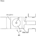
Fig. 6 is a bottom view showing a relationship of a head part, an avoidance part, and the like used in the first embodiment of the present invention. -
Fig. 7 is a side view showing an aspect in which a connection body is installed by use of a jig in the first embodiment of the present invention. -
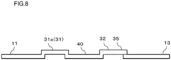
Fig. 8 is a side view showing an aspect in which a connection part and a front surface side sensing terminal are separate. -
Fig. 9 is a perspective view showing a connection body used in a second embodiment of the present invention. - As shown in
Fig. 1 , a semiconductor device, which is an example of an electronic device according to the present embodiment, has a sealingpart 90 being a sealing resin, a firstmain terminal 11 protruding outward from thesealing part 90, and a secondmain terminal 12 protruding outwardly from the sealingpart 90. As shown inFig. 2 , the semiconductor device has asemiconductor element 95 provided in thesealing part 90, thesemiconductor element 95 having a front surface electrically connected to the firstmain terminal 11 and a back surface electrically connected to the secondmain terminal 12, ahead part 40 connected to the front surface of thesemiconductor element 95, asensing terminal 13 of front surface side (hereinafter referred to as a "front surfaceside sensing terminal 13") protruding to the outside from the sealingpart 90 and used for sensing on a source side, and aconnection part 35 integrally formed with thehead part 40 and electrically connected to the front surfaceside sensing terminal 13. Among sensing current paths, a path of a current flowing through the front surface side sensingterminal 13 and theconnection part 35 does not overlap a main current path flowing through the secondmain terminal 12, thesemiconductor element 95, and the first main terminal 11 (SeeFig. 5 ). In the present embodiment, explanation will be made by use of the firstmain terminal 11 through which a main current flows as a first terminal and the front surfaceside sensing terminal 13 through which the main current flows as a second terminal, but the present invention is not limited to this configuration. It is possible to adopt an aspect in which the main current does not flow through the first terminal or use an aspect in which the second terminal is not used for sensing. - In the present embodiment, the semiconductor device is used as the electronic device and the
semiconductor element 95 is used as the electronic element, but the present invention is not limited to this configuration, and the embodiment is not particularly necessary to be a "semiconductor". - As shown in
Fig. 2 , the semiconductor device may have, for example, asubstrate 5 including an insulating material, and aconductive layer 70 provided on thesubstrate 5 and including copper. As shown inFig. 4 , aheat sink 79 including copper may be provided on a back surface of thesubstrate 5. - In the aspect shown in
Fig. 2 , the secondmain terminal 12 is connected to theconductive layer 70, and the secondmain terminal 12 is connected to the back surface of thesemiconductor element 95 via theconductive layer 70. A resist (not shown) may be provided on a periphery of a connection point of the secondmain terminal 12 with theconductive layer 70 to prevent a conductive adhesive such as solder from flowing out. The back surface of thesemiconductor element 95 and theconductive layer 70 may be connected via the conductive adhesive such as solder. Thehead part 40 and the front surface of thesemiconductor element 95 may also be connected via aconductive adhesive 75 such as solder (seeFig. 4 ). - The
semiconductor element 95 may have a withstand voltage structure such as a guard ring. When thesemiconductor element 95 has such a withstand voltage structure,avoidance parts head part 40, for avoiding contact with the withstand voltage structure may be provided as shown inFig. 3 .Such avoidance parts semiconductor element 95, and are designed in advance based on an arrangement position of the withstand voltage structure such as a guard ring, a thickness in a horizontal direction, and the like. - The
avoidance parts first avoidance part 31 provided between the firstmain terminal 11 and thehead part 40, and asecond avoidance part 32 provided between the front surfaceside sensing terminal 13 and thehead part 40. Thefirst avoidance part 31 may be afirst recess part 31a recessed to be away from thesemiconductor element 95, and thesecond avoidance part 32 may be asecond recess part 32a recessed to be away from thesemiconductor element 95. Note that, inFig. 7 , an aspect in which a recess part is not used is shown. - The first
main terminal 11 and the secondmain terminal 12 may be power terminals through which a large current flows. The main current path is formed so as to pass through the secondmain terminal 12, theconductive layer 70, the back surface and the front surface of thesemiconductor element 95, thehead part 40, thefirst avoidance part 31, and the first main terminal 11 (seeFig. 2 ). On the other hand, a sensing current path is formed so as to pass through the front surface of thesemiconductor element 95, thehead part 40, thesecond avoidance part 32, theconnection part 35, and the front surfaceside sensing terminal 13. On one hand, the current flowing from the front surface of thesemiconductor element 95 to thehead part 40 passes through thefirst avoidance part 31 and the firstmain terminal 11 along the main current path, and on the other hand passes through thesecond avoidance part 32, theconnection part 35, and the front surfaceside sensing terminal 13 along the sensing current path. - As shown in
Fig. 2 , the front surfaceside sensing terminal 13 and theconnection part 35 may be integrally formed with thehead part 40. However, the present invention is not limited to this configuration. For example, as shown inFig. 8 , theconnection part 35 and thehead part 40 may be integrally formed, but theconnection part 35 and the front surfaceside sensing terminal 13 may be formed separately. As an example, a back surface of theconnection part 35 may be electrically connected to a front surface of the front surfaceside sensing terminal 13 via a conductive adhesive or the like. - As shown in
Fig. 2 , the firstmain terminal 11 and thehead part 40 may be integrally formed. In the case where the firstmain terminal 11 and thehead part 40 are integrally formed, as shown inFigs. 3 and4 , the firstmain terminal 11 may not be connected to theconductive layer 70, but may be provided away from theconductive layer 70. In this aspect, theconductive layer 70 may not be provided under the firstmain terminal 11, or thefirst avoidance part 31 may be exposed from a side surface of the sealingpart 90 to the outside in the middle of thefirst avoidance part 31, or immediately after thefirst avoidance part 31, the firstmain terminal 11 may be exposed to the outside from the side surface of the sealingpart 90. - In the case where the first
main terminal 11 and thehead part 40 are integrally formed, and the front surfaceside sensing terminal 13, theconnection part 35, and thehead part 40 are integrally formed, as shown inFigs. 3 and7 , a back surface side height of the firstmain terminal 11 and a back surface side height of the front surfaceside sensing terminal 13 may correspond to each other. Here, the fact that the heights correspond to each other means a match within 10% of a thickness of the thicker one of the firstmain terminal 11 and the front surfaceside sensing terminal 13. When thicknesses To of the firstmain terminal 11 and the front surfaceside sensing terminal 13 are the same, deviation between the back surface side height of the firstmain terminal 11 and the back surface side height of the secondmain terminal 12 is within 10% of the thickness T0, which means that it is within 0.1T0. When the thicknesses of the firstmain terminal 11 and the front surfaceside sensing terminal 13 are different, it is within 10% of a thickness T1 of the thicker one, which means that it is within 0.1T1. The back surface side height of the firstmain terminal 11 and the back surface side height of the front surfaceside sensing terminal 13 may match. In the case of the match, it means that the deviation between the back surface side height of the firstmain terminal 11 and the back surface side height of the front surfaceside sensing terminal 13 is within a manufacturing error range. - When the first
main terminal 11 and thehead part 40 are integrally formed and theconnection part 35 and thehead part 40 are integrally formed, the back surface side height of the firstmain terminal 11 and the back surface side height of the front surfaceside sensing terminal 13 coupled with theconnection part 35 may correspond (seeFig. 8 ). Here, similarly to the aspect explained above, the fact that the heights correspond to each other means a match within 10% of the thickness of the thicker one of the firstmain terminal 11 and the front surfaceside sensing terminal 13. The back surface side height of the firstmain terminal 11 and the back surface side height of the front surfaceside sensing terminal 13 may match. In the case of the match, it means that the deviation between the back surface side height of the firstmain terminal 11 and the back surface side height of the front surfaceside sensing terminal 13 is within the manufacturing error range. In the present embodiment, "coupled" also includes an aspect in a form of "integrated". - As shown in
Fig. 2 andFig. 3 , the front surfaceside sensing terminal 13, theconnection part 35, and the firstmain terminal 11 may extend in an opposite direction from thehead part 40. In this case, the firstmain terminal 11 and the front surfaceside sensing terminal 13 maybe used as jig receivers for receiving a jig 99 (Fig. 7 ). However, the front surfaceside sensing terminal 13, theconnection part 35, and the firstmain terminal 11 may extend in different directions as viewed from thehead part 40, and the present invention is not limited to this configuration. For example, the front surfaceside sensing terminal 13, theconnection part 35, and the firstmain terminal 11 may extend to form an angle of 90 degrees or an angle greater than 90 degrees (obtuse angle). - As shown in
Fig. 6 , thehead part 40 may have asecond protrusion unit 42 protruding toward a side of thesemiconductor element 95 and afirst protrusion unit 41 protruding from thesecond protrusion unit 42 toward the side of thesemiconductor element 95. - In the aspect shown in
Fig. 2 , as an example, widths of thefirst avoidance part 31, thehead part 40, and thesecond avoidance part 32 are larger than widths of the front surfaceside sensing terminal 13 and theconnection part 35, and widths of the firstmain terminal 11 and the secondmain terminal 12 are larger than the widths of thefirst avoidance part 31, thehead part 40, and thesecond avoidance part 32. - Through the sensing current path, there is no need to pass a large current, so the widths of the
second avoidance part 32, theconnection part 35, and the front surfaceside sensing terminal 13 may be narrow. As an example, the width of each of thesecond avoidance part 32, theconnection part 35, and the front surfaceside sensing terminal 13 may be narrowed to be one-third or less or one-fifth or less of the width of thehead part 40. Note that, in the aspect shown inFig. 2 , the width of thesecond avoidance part 32 on a side of the head part is large, but the present invention is not limited to this aspect. As shown inFig. 2 , by making the width on the side of the head part of thesecond avoidance part 32 larger and making the width on the side of the head part side correspond to the width of thehead part 40, the width of the planarshape head part 40 of thesecond avoidance part 32 can be surely secured. That is, when thehead part 40, thesecond avoidance part 32, and the like are formed, it is conceivable to punch out a conductive member such as a copper plate, but from a viewpoint of ensuring the width of thehead part 40, it is preferable to set the width of thesecond avoidance part 32 adjacent to thehead part 40 to be approximately equal to the width of thehead part 40. On the other hand, when sacrificing the width of thehead part 40 to some extent, it is also conceivable to narrow the entire width of thesecond avoidance part 32. - In the aspect shown in
Fig. 1 , the secondmain terminal 12, the front surfaceside sensing terminal 13, a back surfaceside sensing terminal 14 and acontrol terminal 15 protrude from the outside from one side surface of the sealingpart 90, and the firstmain terminal 11 protrudes outward from the other side surface of the sealingpart 90. The firstmain terminal 11, the secondmain terminal 12, the front surfaceside sensing terminal 13, the back surfaceside sensing terminal 14, and thecontrol terminal 15 are bent to a front surface side, and are connected to a control substrate (not shown) provided on the front surface side. This control substrate is used to control thesemiconductor element 95. - A structure within the sealing
part 90 of the semiconductor device may be line symmetrical. As an example, each of the firstmain terminal 11, the secondmain terminal 12, the front surfaceside sensing terminal 13, the back surfaceside sensing terminal 14, thecontrol terminal 15, and theconductive layer 70 may be arranged to be axisymmetric with respect to an arbitrary straight line. Awire 19 is also shown inFig. 2 . - Next, operations and effects according to the present embodiment having the above configuration will be explained.
- According to the present embodiment, since the
head part 40 and theconnection part 35 are integrally formed, an influence of a wiring resistance can be prevented as much as possible. In addition, the currents flowing through the front surfaceside sensing terminal 13 and theconnection part 35 among the sensing current path do not overlap with the main current path through the firstmain terminal 11, thesemiconductor element 95 and the second main terminal 12 (SeeFig. 5 ), and therefore, it is also possible to prevent an influence of the wiring resistance caused by the main current path. Therefore, the voltage of thesemiconductor element 95 can be detected more accurately. - In the conventional configuration, the front surface
side sensing terminal 13 for detecting the voltage at thesemiconductor element 95 is connected to theconductive layer 70 connected to a proximal end part of a connector, and therefore, both of the sensing current path for measuring the voltage of thesemiconductor element 95 and the current path flowing through thesemiconductor element 95 pass through at least the same connector, and voltage drop of the wiring resistance of the connector affects the voltage detected by the front surfaceside sensing terminal 13. In contrast, according to the present embodiment, on one hand, the current flowing from the front surface of thesemiconductor element 95 to thehead part 40 passes through thefirst avoidance part 31 and the firstmain terminal 11 along the main current path, and on the other hand, passes through thesecond avoidance part 32, theconnection part 35, and the front surfaceside sensing terminal 13 along the sensing current path. Therefore, the voltage of thesemiconductor element 95 detected by the front surfaceside sensing terminal 13 is detected as a more accurate value. - Note that, when a large current (for example, 200A to 300A or more) flows through the first
main terminal 11 and the secondmain terminal 12, the influence of the voltage drop due to the wiring resistance becomes large. Therefore, when such a large current flows, it is veryuseful to adopt the aspect of the present embodiment. - As shown in
Fig. 2 and the like, when adopting the aspect in which the front surfaceside sensing terminal 13, theconnection part 35, and thehead part 40 are integrally formed, the front surfaceside sensing terminal 13, theconnection part 35, and thehead part 40 can integrally include the same material, and therefore, the voltage to be detected is not affected by a connection mode unlike the case where the front surfaceside sensing terminal 13, theconnection part 35, and thehead part 40 are separated . Therefore, it is advantageous in that the voltage can be detected more accurately by the front surfaceside sensing terminal 13. - As shown in
Fig. 8 , even in the case where thehead part 40 and theconnection part 35 are integrally formed and theconnection part 35 and the front surfaceside sensing terminal 13 are separately formed, when theconnection part 35 and the front surfaceside sensing terminal 13 are connected without passing through theconductive layer 70, the voltage to be detected is not affected by connection modes between theconnection part 35 and theconductive layer 70 and between the front surfaceside sensing terminal 13 and theconductive layer 70. Therefore, it is advantageous in that the voltage can be accurately detected by the front surfaceside sensing terminal 13. - When the first
main terminal 11 and thehead part 40 are integrally formed, theconductive layer 70 for connecting to the firstmain terminal 11 is unnecessary, and theconductive layer 70 may not be provided on a back surface side of the firstmain terminal 11. In the case where theconductive layer 70 is not provided in this manner, the manufacturing cost can be reduced. In the case where the firstmain terminal 11 and thehead part 40 are integrally formed, it is possible to expose the terminal outward from the side surface of the sealingpart 90 without passing through theconductive layer 70. Therefore, it can be expected that a size in an in-plane direction is reduced due to absence of theconductive layer 70. Note that, in the conventional configuration, the front surfaceside sensing terminal 13 for detecting the voltage in thesemiconductor element 95 is connected to theconductive layer 70 connected to the proximal end part of the connector, and therefore, it is necessary to provide such theconductive layer 70. - In the case where the
semiconductor element 95 has the withstand voltage structure, and theavoidance parts head part 40 for avoiding contact with the withstand voltage structure are provided (seeFig. 4 and the like), it is possible to prevent electrical connection between the withstand voltage structure of thesemiconductor element 95 and aconnection body 50. In this aspect, as shown inFig. 2 and the like, when adopting the aspect in which theconnection part 35 is integrally formed with the front surfaceside sensing terminal 13, thesecond avoidance part 32, and thehead part 40, members between thehead part 40 and the front surfaceside sensing terminal 13 can be integrally formed, and there is no change in the current flowing by the connection mode unlike a case where any one of them is separated. Therefore, the voltage or current can be detected more accurately by the front surfaceside sensing terminal 13. - Next, a second embodiment of the present invention will be described.
- In the first embodiment, the explanation was made by use of the aspect in which the
head part 40 and the firstmain terminal 11 are integrally formed. As shown inFig. 9 , aconnection body 50a according to the second embodiment is separate from a firstmain terminal 11 and ahead part 40. In the present embodiment, aproximal end part 45 is formed integrally with thehead part 40 and connected to aconductive layer 70 in a sealingpart 90. - The configuration other than the above is similar to that in the first embodiment. In the second embodiment, the same or similar members or the like as those in the first embodiment are denoted with the same reference numerals, and description thereof is omitted. In the present embodiment, with the exception of the effect obtained in the case where the
head part 40 and the firstmain terminal 11 are integrally formed, the effect similar to the effect achieved by the first embodiment can be obtained. - Lastly, the description of each embodiment described above, the description of the modification, and the disclosure of the drawings are merely examples for explaining the invention described in the claims, and the invention described in the claims is not limited by the description of the above-mentioned embodiment or the disclosure of the drawings. In addition, the description of the claims as filed is merely an example, and the description of the claims can be appropriately changed based on the description of the specification, the drawings, and the like.
-
- 11
- first main terminal
- 12
- second main terminal
- 13
- front surface side sensing terminal
- 31
- first avoidance part
- 32
- second avoidance part
- 35
- connection part
- 40
- head part
- 50, 50a
- connection body
- 70
- conductive layer
- 75
- conductive adhesive
- 90
- sealing part
- 95
- semiconductor element (electronic element)
Claims (6)
- An electronic device comprising:a sealing part;a first main terminal protruding outward from the sealing part;a second main terminal protruding outwardly from the sealing part;an electronic element provided in the sealing part and having a front surface electrically connected to the first main terminal and a back surface electrically connected to the second main terminal;a head part connected to the front surface of the electronic element;a sensing terminal protruding to an outside from the sealing part and used for sensing; anda connection part integrally formed with the head part and electrically connected to the sensing terminal, whereina current flowing through the sensing terminal and the connection part among a sensing current path does not overlap a main current path flowing through the second main terminal, the electronic element and the first main terminal.
- The electronic device according to claim 1, wherein
the sensing terminal and the connection part are integrally formed with the head part. - The electronic device according to claim 2, wherein
the first main terminal and the head part are integrally formed. - The electronic device, according to claim 1 or 2, further comprising
a proximal end part formed integrally with the head part and connected to a conductive layer in the sealing part. - The electronic device according to any one of claims 1 to 4, wherein
the electronic element has a withstand voltage structure,
the electronic device further comprises an avoidance part, formed integrally with the head part, for avoiding contact with the withstand voltage structure. - A connection body used for an electronic device having a sealing part, a first main terminal protruding outward from the sealing part, a second main terminal protruding outwardly from the sealing part and an electronic element provided in the sealing part and having a front surface electrically connected to the first main terminal and a back surface electrically connected to the second main terminal, the connection body comprising:a head part connected to the front surface of the electronic element; anda connection part integrally formed with the head part and electrically connected to a sensing terminal protruding to an outside from the sealing part and used for sensing, whereina current flowing through the connection part among a sensing current path does not overlap a main current path flowing through the second main terminal, the electronic element and the first main terminal.
Applications Claiming Priority (1)
| Application Number | Priority Date | Filing Date | Title |
|---|---|---|---|
| PCT/JP2017/006025 WO2018150555A1 (en) | 2017-02-20 | 2017-02-20 | Electronic device and connector |
Publications (2)
| Publication Number | Publication Date |
|---|---|
| EP3584592A1 true EP3584592A1 (en) | 2019-12-25 |
| EP3584592A4 EP3584592A4 (en) | 2020-11-18 |
Family
ID=63169172
Family Applications (1)
| Application Number | Title | Priority Date | Filing Date |
|---|---|---|---|
| EP17896713.9A Pending EP3584592A4 (en) | 2017-02-20 | 2017-02-20 | ELECTRONIC DEVICE AND CONNECTOR |
Country Status (6)
| Country | Link |
|---|---|
| US (1) | US11211311B2 (en) |
| EP (1) | EP3584592A4 (en) |
| JP (1) | JP6517434B2 (en) |
| KR (1) | KR102282886B1 (en) |
| CN (1) | CN110168388B (en) |
| WO (1) | WO2018150555A1 (en) |
Families Citing this family (2)
| Publication number | Priority date | Publication date | Assignee | Title |
|---|---|---|---|---|
| EP4131370A4 (en) * | 2020-04-01 | 2023-10-11 | Panasonic Intellectual Property Management Co., Ltd. | SEMICONDUCTOR MODULE |
| CN114628347B (en) * | 2022-05-16 | 2022-07-22 | 山东中清智能科技股份有限公司 | Semiconductor packaging structure and preparation method thereof |
Family Cites Families (23)
| Publication number | Priority date | Publication date | Assignee | Title |
|---|---|---|---|---|
| JP2858390B2 (en) | 1994-03-02 | 1999-02-17 | 株式会社デンソー | Method for measuring characteristics of vertical semiconductor device |
| JP3780061B2 (en) | 1997-04-17 | 2006-05-31 | 株式会社日立製作所 | Surface mount semiconductor device |
| US6249041B1 (en) | 1998-06-02 | 2001-06-19 | Siliconix Incorporated | IC chip package with directly connected leads |
| US6307755B1 (en) * | 1999-05-27 | 2001-10-23 | Richard K. Williams | Surface mount semiconductor package, die-leadframe combination and leadframe therefor and method of mounting leadframes to surfaces of semiconductor die |
| JP4623659B2 (en) * | 2006-02-23 | 2011-02-02 | パナソニック株式会社 | Semiconductor device |
| WO2008031029A2 (en) * | 2006-09-08 | 2008-03-13 | Promethean Devices Llc | Sensor, method and system of monitoring transmission lines |
| US20080185596A1 (en) * | 2007-02-02 | 2008-08-07 | Tpo Displays Corp. | System for displaying images |
| JP2008227286A (en) | 2007-03-14 | 2008-09-25 | Sanyo Electric Co Ltd | Semiconductor device and manufacturing method thereof |
| KR20090022512A (en) * | 2007-08-30 | 2009-03-04 | 삼성전자주식회사 | Image sensor and its manufacturing method |
| JP4900148B2 (en) | 2007-09-13 | 2012-03-21 | 三菱電機株式会社 | Semiconductor device |
| JP2009231643A (en) * | 2008-03-24 | 2009-10-08 | Casio Comput Co Ltd | Optical sensing element, photosensor, and display device |
| EP2690658B1 (en) | 2011-03-24 | 2019-11-13 | Mitsubishi Electric Corporation | Power semiconductor module and power unit device |
| JP5267959B2 (en) * | 2011-05-30 | 2013-08-21 | 株式会社デンソー | Semiconductor module and driving device using the same |
| JP2013004943A (en) * | 2011-06-22 | 2013-01-07 | Renesas Electronics Corp | Semiconductor device and manufacturing method thereof |
| US8853835B2 (en) * | 2012-10-05 | 2014-10-07 | Infineon Technologies Ag | Chip arrangements, a chip package and a method for manufacturing a chip arrangement |
| CN103855902A (en) * | 2012-11-28 | 2014-06-11 | 姚其良 | System for detecting working distribution angles of Hall sensors of outer-stator type two-phase direct-current motor |
| CN203275343U (en) * | 2013-05-06 | 2013-11-06 | 海南大学 | Semiconductor ozone sensor measuring circuit |
| EP2830218B1 (en) * | 2013-07-23 | 2021-04-28 | Infineon Technologies AG | Thermal observer and overload protection for power switches |
| US9557351B2 (en) * | 2013-12-18 | 2017-01-31 | Deere & Company | Sensorless current sensing methods for power electronic converters |
| CN203941234U (en) * | 2014-05-27 | 2014-11-12 | 江苏瑞新科技股份有限公司 | A kind of solar power silicon sheet resistivity current vortex proving installation |
| JPWO2015182669A1 (en) * | 2014-05-29 | 2017-04-27 | カルソニックカンセイ株式会社 | Semiconductor switching element drive circuit |
| JP6335815B2 (en) | 2015-02-24 | 2018-05-30 | 三菱電機株式会社 | Heat dissipation structure |
| EP3109649B1 (en) * | 2015-06-25 | 2019-08-07 | ABB Schweiz AG | Aging determination of power semiconductor device in electric drive system |
-
2017
- 2017-02-20 JP JP2018517911A patent/JP6517434B2/en active Active
- 2017-02-20 EP EP17896713.9A patent/EP3584592A4/en active Pending
- 2017-02-20 WO PCT/JP2017/006025 patent/WO2018150555A1/en not_active Ceased
- 2017-02-20 CN CN201780081394.XA patent/CN110168388B/en active Active
- 2017-02-20 KR KR1020197025462A patent/KR102282886B1/en active Active
- 2017-02-20 US US16/468,261 patent/US11211311B2/en active Active
Also Published As
| Publication number | Publication date |
|---|---|
| US11211311B2 (en) | 2021-12-28 |
| EP3584592A4 (en) | 2020-11-18 |
| KR102282886B1 (en) | 2021-07-27 |
| JPWO2018150555A1 (en) | 2019-02-21 |
| JP6517434B2 (en) | 2019-05-22 |
| KR20190112097A (en) | 2019-10-02 |
| US20200011904A1 (en) | 2020-01-09 |
| CN110168388A (en) | 2019-08-23 |
| CN110168388B (en) | 2021-10-22 |
| WO2018150555A1 (en) | 2018-08-23 |
Similar Documents
| Publication | Publication Date | Title |
|---|---|---|
| US10969410B2 (en) | Current sensor device | |
| US9476915B2 (en) | Magnetic field current sensors | |
| EP2733496B1 (en) | Current sensor substrate and current sensor | |
| US9995771B2 (en) | Shunt resistor | |
| CN104034935B (en) | Current sensor | |
| US20190204363A1 (en) | Current sensor | |
| EP2963428A1 (en) | Current sensor and electronic device containing same | |
| US10267824B2 (en) | Shunt resistor | |
| JP6268128B2 (en) | Switch box and overcurrent prevention method | |
| CN111443230B (en) | Current Sensor Device with Routeable Molded Leadframe | |
| US11211311B2 (en) | Electronic device and connection body | |
| US10622313B2 (en) | Shielded electronic device module and method of measuring shielding thereof | |
| WO2018092337A1 (en) | Current sensor | |
| CN214539763U (en) | Current detection device | |
| EP3584831B1 (en) | Electronic device, and connector | |
| EP4043890B1 (en) | Magnetic sensor and current detection device comprising same | |
| EP3584830B1 (en) | Electronic device | |
| JP2020020624A (en) | Magnetic sensor device | |
| WO2016080135A1 (en) | Current sensor | |
| US20230101284A1 (en) | Circuit assembly and electrical junction box | |
| CN109844554A (en) | Magnetic detecting element | |
| US11404353B2 (en) | Electronic device, connection body, and manufacturing method for electronic device |
Legal Events
| Date | Code | Title | Description |
|---|---|---|---|
| STAA | Information on the status of an ep patent application or granted ep patent |
Free format text: STATUS: THE INTERNATIONAL PUBLICATION HAS BEEN MADE |
|
| PUAI | Public reference made under article 153(3) epc to a published international application that has entered the european phase |
Free format text: ORIGINAL CODE: 0009012 |
|
| STAA | Information on the status of an ep patent application or granted ep patent |
Free format text: STATUS: REQUEST FOR EXAMINATION WAS MADE |
|
| 17P | Request for examination filed |
Effective date: 20190918 |
|
| AK | Designated contracting states |
Kind code of ref document: A1 Designated state(s): AL AT BE BG CH CY CZ DE DK EE ES FI FR GB GR HR HU IE IS IT LI LT LU LV MC MK MT NL NO PL PT RO RS SE SI SK SM TR |
|
| AX | Request for extension of the european patent |
Extension state: BA ME |
|
| DAV | Request for validation of the european patent (deleted) | ||
| DAX | Request for extension of the european patent (deleted) | ||
| REG | Reference to a national code |
Ref country code: DE Ref legal event code: R079 Free format text: PREVIOUS MAIN CLASS: G01R0031260000 Ipc: G01R0031280000 |
|
| A4 | Supplementary search report drawn up and despatched |
Effective date: 20201015 |
|
| RIC1 | Information provided on ipc code assigned before grant |
Ipc: H01L 23/498 20060101ALI20201009BHEP Ipc: H01L 23/48 20060101ALI20201009BHEP Ipc: H01L 23/373 20060101ALN20201009BHEP Ipc: G01R 31/26 20200101ALI20201009BHEP Ipc: G01R 31/28 20060101AFI20201009BHEP Ipc: H01L 23/495 20060101ALI20201009BHEP |
|
| STAA | Information on the status of an ep patent application or granted ep patent |
Free format text: STATUS: EXAMINATION IS IN PROGRESS |
|
| 17Q | First examination report despatched |
Effective date: 20230117 |