EP3582291B1 - Batteriemodul - Google Patents
Batteriemodul Download PDFInfo
- Publication number
- EP3582291B1 EP3582291B1 EP18191809.5A EP18191809A EP3582291B1 EP 3582291 B1 EP3582291 B1 EP 3582291B1 EP 18191809 A EP18191809 A EP 18191809A EP 3582291 B1 EP3582291 B1 EP 3582291B1
- Authority
- EP
- European Patent Office
- Prior art keywords
- conductive
- circuit board
- sleeve
- sampling circuit
- conductive sleeve
- Prior art date
- Legal status (The legal status is an assumption and is not a legal conclusion. Google has not performed a legal analysis and makes no representation as to the accuracy of the status listed.)
- Active
Links
Images


Classifications
-
- H—ELECTRICITY
- H01—ELECTRIC ELEMENTS
- H01M—PROCESSES OR MEANS, e.g. BATTERIES, FOR THE DIRECT CONVERSION OF CHEMICAL ENERGY INTO ELECTRICAL ENERGY
- H01M10/00—Secondary cells; Manufacture thereof
- H01M10/42—Methods or arrangements for servicing or maintenance of secondary cells or secondary half-cells
- H01M10/425—Structural combination with electronic components, e.g. electronic circuits integrated to the outside of the casing
-
- H—ELECTRICITY
- H01—ELECTRIC ELEMENTS
- H01M—PROCESSES OR MEANS, e.g. BATTERIES, FOR THE DIRECT CONVERSION OF CHEMICAL ENERGY INTO ELECTRICAL ENERGY
- H01M10/00—Secondary cells; Manufacture thereof
- H01M10/42—Methods or arrangements for servicing or maintenance of secondary cells or secondary half-cells
- H01M10/48—Accumulators combined with arrangements for measuring, testing or indicating the condition of cells, e.g. the level or density of the electrolyte
- H01M10/482—Accumulators combined with arrangements for measuring, testing or indicating the condition of cells, e.g. the level or density of the electrolyte for several batteries or cells simultaneously or sequentially
-
- H—ELECTRICITY
- H01—ELECTRIC ELEMENTS
- H01M—PROCESSES OR MEANS, e.g. BATTERIES, FOR THE DIRECT CONVERSION OF CHEMICAL ENERGY INTO ELECTRICAL ENERGY
- H01M50/00—Constructional details or processes of manufacture of the non-active parts of electrochemical cells other than fuel cells, e.g. hybrid cells
- H01M50/20—Mountings; Secondary casings or frames; Racks, modules or packs; Suspension devices; Shock absorbers; Transport or carrying devices; Holders
- H01M50/204—Racks, modules or packs for multiple batteries or multiple cells
- H01M50/207—Racks, modules or packs for multiple batteries or multiple cells characterised by their shape
- H01M50/209—Racks, modules or packs for multiple batteries or multiple cells characterised by their shape adapted for prismatic or rectangular cells
-
- H—ELECTRICITY
- H01—ELECTRIC ELEMENTS
- H01M—PROCESSES OR MEANS, e.g. BATTERIES, FOR THE DIRECT CONVERSION OF CHEMICAL ENERGY INTO ELECTRICAL ENERGY
- H01M50/00—Constructional details or processes of manufacture of the non-active parts of electrochemical cells other than fuel cells, e.g. hybrid cells
- H01M50/50—Current conducting connections for cells or batteries
-
- H—ELECTRICITY
- H01—ELECTRIC ELEMENTS
- H01M—PROCESSES OR MEANS, e.g. BATTERIES, FOR THE DIRECT CONVERSION OF CHEMICAL ENERGY INTO ELECTRICAL ENERGY
- H01M50/00—Constructional details or processes of manufacture of the non-active parts of electrochemical cells other than fuel cells, e.g. hybrid cells
- H01M50/50—Current conducting connections for cells or batteries
- H01M50/502—Interconnectors for connecting terminals of adjacent batteries; Interconnectors for connecting cells outside a battery casing
- H01M50/503—Interconnectors for connecting terminals of adjacent batteries; Interconnectors for connecting cells outside a battery casing characterised by the shape of the interconnectors
-
- H—ELECTRICITY
- H01—ELECTRIC ELEMENTS
- H01M—PROCESSES OR MEANS, e.g. BATTERIES, FOR THE DIRECT CONVERSION OF CHEMICAL ENERGY INTO ELECTRICAL ENERGY
- H01M50/00—Constructional details or processes of manufacture of the non-active parts of electrochemical cells other than fuel cells, e.g. hybrid cells
- H01M50/50—Current conducting connections for cells or batteries
- H01M50/502—Interconnectors for connecting terminals of adjacent batteries; Interconnectors for connecting cells outside a battery casing
- H01M50/519—Interconnectors for connecting terminals of adjacent batteries; Interconnectors for connecting cells outside a battery casing comprising printed circuit boards [PCB]
-
- H—ELECTRICITY
- H01—ELECTRIC ELEMENTS
- H01M—PROCESSES OR MEANS, e.g. BATTERIES, FOR THE DIRECT CONVERSION OF CHEMICAL ENERGY INTO ELECTRICAL ENERGY
- H01M50/00—Constructional details or processes of manufacture of the non-active parts of electrochemical cells other than fuel cells, e.g. hybrid cells
- H01M50/50—Current conducting connections for cells or batteries
- H01M50/502—Interconnectors for connecting terminals of adjacent batteries; Interconnectors for connecting cells outside a battery casing
- H01M50/521—Interconnectors for connecting terminals of adjacent batteries; Interconnectors for connecting cells outside a battery casing characterised by the material
- H01M50/522—Inorganic material
-
- H—ELECTRICITY
- H01—ELECTRIC ELEMENTS
- H01M—PROCESSES OR MEANS, e.g. BATTERIES, FOR THE DIRECT CONVERSION OF CHEMICAL ENERGY INTO ELECTRICAL ENERGY
- H01M50/00—Constructional details or processes of manufacture of the non-active parts of electrochemical cells other than fuel cells, e.g. hybrid cells
- H01M50/50—Current conducting connections for cells or batteries
- H01M50/528—Fixed electrical connections, i.e. not intended for disconnection
-
- H—ELECTRICITY
- H01—ELECTRIC ELEMENTS
- H01R—ELECTRICALLY-CONDUCTIVE CONNECTIONS; STRUCTURAL ASSOCIATIONS OF A PLURALITY OF MUTUALLY-INSULATED ELECTRICAL CONNECTING ELEMENTS; COUPLING DEVICES; CURRENT COLLECTORS
- H01R12/00—Structural associations of a plurality of mutually-insulated electrical connecting elements, specially adapted for printed circuits, e.g. printed circuit boards [PCB], flat or ribbon cables, or like generally planar structures, e.g. terminal strips, terminal blocks; Coupling devices specially adapted for printed circuits, flat or ribbon cables, or like generally planar structures; Terminals specially adapted for contact with, or insertion into, printed circuits, flat or ribbon cables, or like generally planar structures
- H01R12/50—Fixed connections
- H01R12/51—Fixed connections for rigid printed circuits or like structures
- H01R12/55—Fixed connections for rigid printed circuits or like structures characterised by the terminals
- H01R12/58—Fixed connections for rigid printed circuits or like structures characterised by the terminals terminals for insertion into holes
-
- H—ELECTRICITY
- H05—ELECTRIC TECHNIQUES NOT OTHERWISE PROVIDED FOR
- H05K—PRINTED CIRCUITS; CASINGS OR CONSTRUCTIONAL DETAILS OF ELECTRIC APPARATUS; MANUFACTURE OF ASSEMBLAGES OF ELECTRICAL COMPONENTS
- H05K1/00—Printed circuits
- H05K1/02—Details
- H05K1/11—Printed elements for providing electric connections to or between printed circuits
- H05K1/115—Via connections; Lands around holes or via connections
-
- H—ELECTRICITY
- H01—ELECTRIC ELEMENTS
- H01M—PROCESSES OR MEANS, e.g. BATTERIES, FOR THE DIRECT CONVERSION OF CHEMICAL ENERGY INTO ELECTRICAL ENERGY
- H01M10/00—Secondary cells; Manufacture thereof
- H01M10/42—Methods or arrangements for servicing or maintenance of secondary cells or secondary half-cells
- H01M10/425—Structural combination with electronic components, e.g. electronic circuits integrated to the outside of the casing
- H01M2010/4271—Battery management systems including electronic circuits, e.g. control of current or voltage to keep battery in healthy state, cell balancing
-
- H—ELECTRICITY
- H01—ELECTRIC ELEMENTS
- H01M—PROCESSES OR MEANS, e.g. BATTERIES, FOR THE DIRECT CONVERSION OF CHEMICAL ENERGY INTO ELECTRICAL ENERGY
- H01M2200/00—Safety devices for primary or secondary batteries
- H01M2200/10—Temperature sensitive devices
- H01M2200/103—Fuse
-
- H—ELECTRICITY
- H01—ELECTRIC ELEMENTS
- H01M—PROCESSES OR MEANS, e.g. BATTERIES, FOR THE DIRECT CONVERSION OF CHEMICAL ENERGY INTO ELECTRICAL ENERGY
- H01M2220/00—Batteries for particular applications
- H01M2220/20—Batteries in motive systems, e.g. vehicle, ship, plane
-
- H—ELECTRICITY
- H05—ELECTRIC TECHNIQUES NOT OTHERWISE PROVIDED FOR
- H05K—PRINTED CIRCUITS; CASINGS OR CONSTRUCTIONAL DETAILS OF ELECTRIC APPARATUS; MANUFACTURE OF ASSEMBLAGES OF ELECTRICAL COMPONENTS
- H05K2201/00—Indexing scheme relating to printed circuits covered by H05K1/00
- H05K2201/10—Details of components or other objects attached to or integrated in a printed circuit board
- H05K2201/10007—Types of components
- H05K2201/10037—Printed or non-printed battery
-
- H—ELECTRICITY
- H05—ELECTRIC TECHNIQUES NOT OTHERWISE PROVIDED FOR
- H05K—PRINTED CIRCUITS; CASINGS OR CONSTRUCTIONAL DETAILS OF ELECTRIC APPARATUS; MANUFACTURE OF ASSEMBLAGES OF ELECTRICAL COMPONENTS
- H05K2201/00—Indexing scheme relating to printed circuits covered by H05K1/00
- H05K2201/10—Details of components or other objects attached to or integrated in a printed circuit board
- H05K2201/10227—Other objects, e.g. metallic pieces
- H05K2201/10272—Busbars, i.e. thick metal bars mounted on the printed circuit board [PCB] as high-current conductors
-
- H—ELECTRICITY
- H05—ELECTRIC TECHNIQUES NOT OTHERWISE PROVIDED FOR
- H05K—PRINTED CIRCUITS; CASINGS OR CONSTRUCTIONAL DETAILS OF ELECTRIC APPARATUS; MANUFACTURE OF ASSEMBLAGES OF ELECTRICAL COMPONENTS
- H05K2201/00—Indexing scheme relating to printed circuits covered by H05K1/00
- H05K2201/10—Details of components or other objects attached to or integrated in a printed circuit board
- H05K2201/10227—Other objects, e.g. metallic pieces
- H05K2201/10295—Metallic connector elements partly mounted in a hole of the PCB
-
- Y—GENERAL TAGGING OF NEW TECHNOLOGICAL DEVELOPMENTS; GENERAL TAGGING OF CROSS-SECTIONAL TECHNOLOGIES SPANNING OVER SEVERAL SECTIONS OF THE IPC; TECHNICAL SUBJECTS COVERED BY FORMER USPC CROSS-REFERENCE ART COLLECTIONS [XRACs] AND DIGESTS
- Y02—TECHNOLOGIES OR APPLICATIONS FOR MITIGATION OR ADAPTATION AGAINST CLIMATE CHANGE
- Y02E—REDUCTION OF GREENHOUSE GAS [GHG] EMISSIONS, RELATED TO ENERGY GENERATION, TRANSMISSION OR DISTRIBUTION
- Y02E60/00—Enabling technologies; Technologies with a potential or indirect contribution to GHG emissions mitigation
- Y02E60/10—Energy storage using batteries
Definitions
- the present disclosure relates to a technical filed of battery, and particularly to a battery module.
- a secondary battery has begun to be widely used in the field of automobiles.
- a battery management system has to monitor important physical parameters, such as voltage and temperature, of each secondary battery in the battery module in real time, and evaluate and calculate a situation of all secondary batteries in the battery pack by using these physical parameters as an important basis, so as to prevent overcharge and over discharge to ensure a lifetime and safety of the battery system, and make corresponding adjustment strategies.
- the battery management system monitors the secondary battery by means of a sampling connection structure.
- sampling connection structure due to a number of factors, such as automobile vibration and high-voltage discharge, an overload fuse failure, mechanical connection failure, or physical contact wear and rupture, which may lead to an external short-circuit of the secondary battery, resulting in thermal runaway, may occur to the sampling connection, reducing a reliability and safety of the entire vehicle operation of electric vehicles and thus imposing a great negative impact on a sustainable development of an electric vehicle market.
- a pin is directly provided on the busbar, and a hole is provided in the sampling circuit board.
- the sampling connection in the battery module is achieved by directly inserting the pin of the bus bar into the hole provided in the sampling circuit board so that the pin is electrically connected to the sampling circuit board.
- the sampling circuit board includes a conductive layer having a small thickness and an outer insulating layer encasing the conductive layer, in the state that the pin of the busbar is inserted into the hole of the sampling circuit board, only a small contact area can be formed between the entire pin and the conductive layer, and the contact area is less than or equal to an area of the conductive layer exposed within the hole.
- the contact area between the busbar and the sampling circuit board is small, resulting in that a stable contact between the pin of the busbar and the conductive layer of the circuit board cannot be ensured.
- an unstable connection or even disconnection between the pin of the busbar and the conductive layer of the sampling circuit board may occur, resulting in inaccurate sampling data or loss of data, which seriously affects an operational reliability and safety of the battery module during usage.
- JP 2014120417A and US 2014/127554A1 disclose a battery pack, which includes a plurality of batteries, a lead plate, and a circuit board.
- the plurality of batteries are connected with one another.
- the lead plate are connected with the plurality of batteries, and made of a conductive material.
- the circuit board is connected with the plurality of batteries through the lead plate.
- the circuit board includes insertion holes passing through the circuit board along the thickness thereof.
- the lead plate includes an insertion part disposed in the insertion hole. The insertion part is folded and is thicker than the other part of the lead plate.
- JP 200834296A and JP 2005317460A cited in JP 2014120417A and US 2014/127554A1 disclose a battery pack including a lead plate directly connected with a circuit board.
- US 2012/052331A1 discloses a battery pack including a connection circuit board.
- the battery pack includes a multi-cell, a connection circuit board connected to the unit cells, a conductive lead drawn out from the connection circuit board, a printed circuit module having an opening into which the conductive lead is inserted, a solder portion formed by solder connection in which the conductive lead is inserted into the opening, wherein the conductive lead has an insertion portion inserted into the opening, a bent portion bent from the insertion portion, and a recess by which the insertion portion is divided.
- US 2009/246615A1 discloses a battery pack, which includes: a multi-cell battery having a positive electrode and a negative electrode, in which a plurality of battery cells are electrically connected to each other; a protective circuit board electrically connected to the multi-cell battery and having via holes; a pair of conductive tabs each including an insert portion inserted into a corresponding via hole and a bending portion integrally extending from the insert portion and bent from the insert portion; and a pair of soldering portions each being formed at at least some portions of a corresponding insert portion and a corresponding bending portion.
- CN 104282870A and US 2015/017484A1 disclose a battery pack, which includes a plurality of unit batteries arranged side by side in a first direction, each unit battery including a can accommodating an opening including an electrode assembly having a first electrode plate, a second electrode plate, and a separator between the electrode plates, and a cap plate sealing the opening.
- the plurality of unit batteries may be arranged side by side in the first direction with all the cap plates exposed in the same direction.
- the battery pack may further include a protection circuit module adjacent to the cap plate with a circuit board extending in the first direction and a protection device coupled to it, wherein each unit battery further includes a first terminal on a first area of the cap plate and a second terminal on a second area of the cap plate, each coupled to the unit battery and the protection circuit module.
- JP 2009163932A discloses a battery pack, which includes: flat battery cells each having an electrochemical power generation element, an outer packaging sealing the battery cell, and leads of a positive electrode and a negative electrode; a wiring board in which a slot part into which the leads of each cell are inserted in the stacked state of a plurality of battery cells, and a wiring pattern connecting in series and/or in parallel each lead inserted into the slot part with other lead are formed; a sheet-like member for heat insulation and buffer (a heat insulation buffer member); a case member having insulation properties in which the battery cells, the wiring board, and the heat insulation buffer member are housed; and a battery terminal connected to the wiring pattern of the wiring board and exposed to the outside of the case member, and the heat insulating buffer member is arranged between the cells of the stacked batteries.
- JP 2006073457 cited in JP 2009163932A provides battery cells accommodated in an exterior material and having leads from which a positive electrode and a negative electrode are led to the outside from one side of the battery cells.
- the battery module of an embodiment of the disclosure includes a busbar and a sampling circuit board electrically connected with each other, connection of which is stable, reliable and has a high impact resistant ability, and thus operational reliability and safety of the battery module can be improved.
- a battery module comprising:
- a dimension of the filler gap in a radial direction of the conductive sleeve is in a range of 0.1 mm to 0.5 mm.
- the soldered body is configured to occupy at least 75% of the filler gap in an axial direction of the conductive sleeve.
- the conductive sleeve has a wall thickness greater than or equal to 0.025 mm and less than or equal to 1 mm.
- the conductive sleeve is made of copper or a copper alloy.
- a free end of the conductive post away from the connecting plate protrudes beyond a surface of the sampling circuit board.
- the connecting plate is disposed above the sampling circuit board, and the conductive post is inserted into the conductive sleeve from top to bottom.
- the conductive post is formed in a shape of prism, and has a top end surface and a guiding bevel in connection and intersecting with the top end surface.
- the conductive post included in the busbar of the present disclosure is directly electrically connected to the conductive sleeve of the sampling circuit board.
- a contact area between the conductive post and the conductive sleeve is large and a contact between them is tight, so that an offset or separation between the conductive post and the conductive sleeve is less likely to occur, stability of connection between the conductive post and the conductive sleeve can be improved, stability of an electrical connection between the busbar and the sampling circuit board can be effectively ensured, and a possibility of unstable connection or open circuit between the busbar and the sampling circuit board can be reduced.
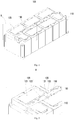
- a battery module 100 according to an embodiment of the present disclosure will be described in detail below.
- the battery module 100 of the embodiment of the present disclosure includes a plurality of single cells 110 arranged in one direction, a busbar 120 electrically connected to the single cells 110, and a sampling circuit board 130 for sampling physical parameters of the single cells 110.
- Adjacent single cells 110 may be connected in series or in parallel by the busbar 120 of the embodiment.
- the busbar 120 is directly electrically connected to the sampling circuit board 130.
- the sampling circuit board 130 of the embodiment is disposed on a top of the single cells 110. The top refers to a side of the single cells 110 to be electrically connected with each other.
- the sampling circuit board 130 of the embodiment may be a rigid circuit board or a flexible circuit board.
- the sampling circuit board 130 of the embodiment extends in the arrangement direction of the single cells 110.
- the sampling circuit board 130 of the embodiment has an upper surface and a lower surface opposite to each other, wherein the lower surface of the sampling circuit board 130 is disposed facing the single cells 110 when the sampling circuit board 130 is disposed on the top of the single cells 110.
- the sampling circuit board 130 of the embodiment includes a conductive layer 130a, an external insulating layer 130b encasing the conductive layer 130a, and a conductive hole 131 extending from the upper surface to the lower surface of the sampling circuit board 130.
- a section of the conductive layer 130a is exposed in the conductive hole 131, so that the section of the conductive layer 130a can be directly observed at the conductive hole 131.
- the sampling circuit board 130 of the embodiment further includes a conductive sleeve 132 disposed in the conductive hole 131.
- the conductive sleeve 132 is formed into a hollow structure with a central hole.
- At least a portion of the conductive sleeve 132 is disposed in the conductive hole 131 and tightly mated with the conductive hole 131.
- the conductive sleeve 132 and the section of the conductive layer 130a are tightly contacted and electrically connected with each other, thereby improving vibration resistance of the conductive sleeve 132 and ensuring stability of connection between the conductive sleeve 132 and the conductive layer 130a.
- the conductive sleeve 132 functions as a connecting member for the conductive layer 130a, so that the conductive layer 130a can be electrically connected to an external structural member through the conductive sleeve 132, thereby increasing a contact area of an electrical connection between the external structural member and the sampling circuit board 130.
- the conductive sleeve 132 and the conductive layer 130a are formed into an integral structure.
- the conductive sleeve 132 is formed by electroplating in the conductive hole 131, so that the conductive sleeve 132 and the conductive layer 130a can be formed into an integral structure.
- the conductive sleeve 132 cannot displace in the conductive hole 131 along an axial direction of the conductive hole 131, so that the conductive sleeve 132 can be connected stably and reliably with the conductive layer 130a included in the sampling circuit board 130.
- the conductive sleeve 132 and the conductive layer 130a are formed into separated parts.
- the conductive sleeve 132 and the conductive hole 131 are welded to each other. During the welding, a contact area between the conductive sleeve 132 and the conductive layer 130a are melted. After cooling, a welded area is formed between the conductive sleeve 132 and the conductive layer 130a, which ensures that an outer peripheral surface of the conductive sleeve 132 and the section of the conductive layer 130a are engaged with each other, thereby effectively improving vibration resistance of the conductive sleeve 132.
- the displacement of the conductive sleeve 132 in the conductive hole 131 along the axial direction of the conductive hole 131 is less likely to occur, thereby ensuring the stability and reliability of connection between the conductive sleeve 132 and the conductive layer 130a.
- the busbar 120 of the embodiment includes a connecting plate 121 and a conductive post 122 extending outward from the connecting plate 121.
- the connecting plate 121 included in the busbar 120 is used to be electrically connected to electrode terminals of the single cells 110.
- the conductive post 122 included in the busbar 120 is used to be inserted into the conductive sleeve 132 included in the sampling circuit board 130 so that the busbar 120 and the sampling circuit board 130 are electrically connected.
- the conductive post 122 included in the busbar 120 is directly electrically connected to the conductive sleeve 132 of the sampling circuit board 130.
- a contact area between the conductive post 122 and the conductive sleeve 132 is large and a contact between them is tight, so that an offset or separation between the conductive post 122 and the conductive sleeve 132 is less likely to occur, and stability and vibration resistance of connection between the conductive post 122 and the conductive sleeve 132 are improved, thereby effectively ensuring stability of an electrical connection between the busbar 120 and the sampling circuit board 130 and reducing a possibility of unstable connection or open circuit between the busbar 120 and the sampling circuit board 130.
- the conductive post 122 and the central hole of the conductive sleeve 132 are assembled in an interference fit.
- the conductive post 122 can be pressed into the central hole of the conductive sleeve 132 by being applied to a sufficient pressure.
- a cross section of the central hole of the conductive sleeve 132 is circular or polygonal, and the conductive post 122 is formed with a cross section in a shape of matching with the cross sectional of the central hole of the conductive sleeve 132, so that the central hole of the conductive sleeve 132 and the conductive post 122 can tightly mating with each other.
- the interference fit between the conductive post 122 and the conductive sleeve 132 can ensure that the outer peripheral surface of the conductive post 122 and the inner peripheral surface of the conductive sleeve 132 are pressed to each other, thereby effectively improving friction between them and improving a vibration resistance of a connecting area between the conductive post 122 and the conductive sleeve 132, and thus ensuring stability and reliability of connection between the conductive post 122 and the conductive sleeve 132.
- the conductive post 122 and the conductive sleeve 132 are connected with each other by soldering.
- a diameter of the conductive post 122 is smaller than that of the central hole of the conductive sleeve 132 to form a filler gap 99 with an annular cross section between the outer peripheral surface of the conductive post 122 and the inner wall of the conductive sleeve 132.
- the battery module 100 of the embodiment further includes a soldered body 140 formed by solder.
- the filler gap 99 formed between the conductive post 122 and the inner wall of the conductive sleeve 132 is filled with a solder in a molten state.
- the solder solidifies and forms a soldered body 140 between the conductive post 122 and the conductive sleeve 132.
- the conductive post 122 and the conductive sleeve 132 are connected, fixed and electrically connected by the soldered body 140.
- the soldered body 140 is provided to improve the strength and vibration resistance of connection between the conductive post 122 and the conductive sleeve 132. At least a portion of the soldered body 140 is provided in the filler gap 99.
- the above-described solder may be tin or a tin alloy, and further may be other metal materials suitable for soldering, such as copper.
- the conductive sleeve 132 of the embodiment can isolate the solder at a high temperature from the sampling circuit board 130, thereby reducing a possibility that the solder at a high temperature damages the sampling circuit board 130, and ensuring that the sampling circuit board 130 is not susceptible to high temperature damage or external force impact damage so as to maintain its integrity during connecting operation between the busbar 120 and the sampling circuit board 130.
- the cross section of the central hole of the conductive sleeve 132 may be circular or polygonal, and the shape of the cross section of the conductive post 122 is formed to match with that of the central hole of the conductive sleeve 132, so that a equidistant gap can be formed between the conductive sleeve 132 and the conductive post 122.
- the central hole of the conductive sleeve 132 can be formed as a waist-shaped hole (that is, an oblong hole), and the cross section of the conductive post 122 is rectangular.
- a dimension R of the filler gap 99 is in a range of 0.1 mm to 0.5 mm.
- the soldered body 140 is provided to occupy at least 75% of the entire filler gap 99 in the axial direction of the conductive sleeve 132. In the case that the soldered body 140 occupies less than 75% of the filler gap 99, a filling amount of the soldered body 140 in the filler gap 99 is too small, which will cause an unstable connection between the conductive post 122 and the conductive sleeve 132, and a separation between the conductive post 122 and the conductive sleeve 132 may occur.
- the conductive post 122 has a free end that is away from the connecting plate 121. After the conductive post 122 is inserted into the conductive sleeve 132, the free end of the conductive post 122 protrudes beyond a surface of the sampling circuit board 130.
- the free end of the conductive post 122 can direct the molten solder, so that the molten solder can smoothly flow into the filler gap 99 without overflowing to the surface of the sampling circuit board 130, which reduces a possibility that the solder falls on the surface of the sampling circuit board 130 and burns or damages the sampling circuit board 130, and effectively ensuring a structural integrity of the sampling circuit board 130.
- the sampling circuit board 130 of the embodiment further includes an annular body 133 located at an end of the conductive sleeve 132.
- the annular body 133 is disposed on a surface of the sampling circuit board 130 facing the single cells 110 and is provided to surround the conductive hole 131.
- the annular body 133 of the embodiment may be integrally formed with the conductive sleeve 132, or may be a separate structure from the conductive sleeve 132.
- the soldered body 140 includes a sleeve portion 141 and an annular flange 142 provided on the sleeve portion 141.
- the sleeve portion 141 is disposed in the filler gap 99, and the annular flange 142 extends from the sleeve portion over a surface of the annular body 133. Since the annular flange 142 and the annular body 133 of the conductive sleeve 132 in an axial direction of the conductive hole 131, the annular flange 142 of the soldered body 140 is pressed against the sampling circuit board 130 and thus is further limited by the sampling circuit board 130, which reduces deformation and displacement of the soldered body 140 in the axial direction of the conductive hole 131 when the battery module 100 is subjected to an external vibration and thus ensures the stability and reliability of connection between the conductive post 122 and the conductive sleeve 132.
- the conductive sleeve 132 has a wall thickness D greater than or equal to 0.025 mm.
- D the wall thickness of the conductive sleeve 132 is less than or equal to 1 mm.
- the conductive sleeve 132 is made of copper or a copper alloy which has good electrical conductivity and makes the conductive sleeve 132 and the conductive post 122 to be easily soldered, to ensure a strong connection strength and a stable connection of the conductive sleeve 132 and the conductive post 122, thereby further reducing a possibility of mechanical fracture failure between them.
- the conductive post 122 of the embodiment may be formed in a shape of prism.
- the central hole of the conductive sleeve 132 is formed into a waist-shaped hole (that is, an oblong hole).
- the cross section of the conductive post 122 is rectangular and thus the conductive post 122 is in a shape of quadrangular prism.
- the cross section of the central hole of the conductive sleeve 132 is polygonal, and the cross section of the conductive post 122 is also polygonal and is formed to match with the shape of the central hole of the conductive sleeve 132, so that a portion of the conductive post 122 inserted into the central hole of the conductive sleeve 132 are easily connected and tightly mating with the central hole of the conductive sleeve 132 by an interference fit, so as to improve the stability of connection between the conductive post 122 and the conductive sleeve 132.
- the connecting plate 121 of the embodiment includes a body portion 121a and a cantilever portion 121b extending outward from the body portion 121a.
- the body portion 121a is used to be electrically connected to the electrode terminals of the single cells 110.
- the conductive post 122 is provided at a free end of the cantilever portion 121b.
- An end of the conductive post 122 away from the free end of the cantilever portion 121b has a top end surface 122a and a guiding bevel 122b in connection and intersecting with the top end surface 122a.
- the guide bevel 122b is inclined from the top end surface 122a toward the cantilever portion 121b.
- the conductive post 122 can be inserted into the central hole of the conductive sleeve 132 more quickly and accurately under the guidance of the guiding bevel 122b.
- assembly time can be shorted.
- a possibility that the end of the conductive post 122 and the conductive sleeve 132 are scraped by each other and thus being damaged can be reduced, and thus a possibility that the end of the conductive post 122 and the conductive sleeve 132 are scraped by each other and thus generating debris, which may cause a short circuit between other electrical components, can be reduced. Therefore, the safety of the battery module 100 can be improved.
- the top end surface 122a may be a flat surface or an arc-shaped surface.
- the guiding bevel 122b may be a flat surface or an arc-shaped surface.
- the conductive post 122 has a predetermined width L.
- the top end surface 122a and the guiding bevel 122b of the conductive post 122 are arranged in a width direction X of the conductive post 122.
- the ratio of a width D of an orthographic projection of the guiding bevel 122b in an extending direction Y of the conductive post 122 to the predetermined width L of the conductive poste 122 is in a range of 1/4 to 2/5.
- a component force toward an axis of the central hole of the conductive sleeve 132 applied to the guiding bevel 122b by the sampling circuit board 130 is larger, which is conducive to guide the conductive post 122 to move faster toward the central hole of the conductive sleeve 132 and finally enter the central hole of the conductive sleeve 132.
- the two guiding bevels 122b are respectively provided on two opposite sides of the top end surface 122a.
- the busbar 120 of the embodiment has a groove 123 provided between the cantilever portion 121b and the body portion 121a.
- the single groove 123 is provided on one of two opposite sides of the cantilever portion 121b.
- the groove 123 provided between the cantilever portion 121b and the body portion 121a on one hand, can effectively eliminate stress concentration between the cantilever portion 121b and the body portion 121a, and on the other hand, can improve elastic deformation ability of the cantilever portion 121b.
- the cantilever portion 121b in the case that the conductive post 122 is subjected to an external force, it is easy for the cantilever portion 121b to swing at a predetermined amplitude by self-deformation to counteract or buffer the influence of the external force, and thus reducing a possibility of a fracture failure at the connection between the cantilever portion 121b and the body portion 121a, and improving the stability and vibration resistance of connection between the conductive post 122 and the conductive sleeve 132.
- the connecting plate 121 and the conductive post 122 are formed into an integral structure, so that connection between the conductive post 122 and the connecting plate 121 is strong with a stronger impact resistance ability.
- the busbar 120 can be obtained by punching a plate-like blank.
- the connecting plate 121 of the embodiment is disposed above the sampling circuit board 130, and the conductive post 122 is inserted into the conductive sleeve 132 from top to bottom.
- the term "from top to bottom” here also means that the conductive post 122 is moved toward the single cells 110.
- the sampling circuit board 130 is located between the connecting plate 121 and the single cells 110.
- the busbar 120 is mounted and fixed after the sampling circuit board 130 is mounted at a predetermined position on the top of the single cells 110, and thus the mounting process is optimized. Meanwhile, the conductive post 122 of the busbar 120 can limit a position of the sampling circuit board 130, which can reduce a displacement amount of upper and lower movements when the sampling circuit board 130 is subjected to an external vibration. Therefore, a possibility of mechanical fracture failure of connection between the conductive post 122 and the conductive sleeve 132 is further reduced.
- the sampling circuit board 130 of the embodiment further includes a sampling circuit electrically connected to the conductive hole 131 and a fuse component 150 connected in series between the sampling circuit and the conductive hole 131.
- the fuse component 150 can automatically fuses to prevent the secondary battery from the external short-circuit state of a long time, thereby ensuring safe and stable usage of the secondary battery.
- the fuse component 150 can be a SMD fuse or a slim copper wire embedded in the sampling loop.
- the battery module 100 of the embodiment includes a busbar 120 for electrically connecting with at least two adjacent single cells 110 and a sampling circuit board 130 for collecting parameters, such as voltage and/or temperature, of at least two adjacent single cells 110.
- the conductive post 122 included in the busbar 120 are indirectly electrically connected to the conductive layer 130a of the sampling circuit board 130 via the conductive sleeve 132 of the sampling circuit board 130.
- the contact area between the conductive post 122 and the conductive sleeve 132 of the sampling circuit board 130 is large and the conductive post 122 and the conductive sleeve 132 are tightly contacted with each other, so that offset and separation between the conductive post 122 and the conductive sleeve 132 is less likely to occur, the stability and vibration resistance of connection between the conductive post 122 and the conductive sleeve 132 can be improved, the stability of electrical connection between the busbar 120 and the sampling circuit board 130 can be ensured, and a possibility of unstable connection or disconnection between the busbar 120 and the sampling circuit board 130 can be reduced.
- the conductive post 122 respectively included in the adjacent two busbars 120 will not move and then contact with each other, thereby avoiding an external short circuit of the secondary battery.
- connection between the busbar 120 and the sampling circuit board 130 is still stable, thereby ensuring the reliability and safety of the battery module 100 during usage.
- the technical features mentioned in the various embodiments can be combined in any manner as long as there is no structural conflict. The present disclosure is not limited to the specific embodiments disclosed herein, but includes all technical solutions falling within the scope of the claims.
Landscapes
- Chemical & Material Sciences (AREA)
- Chemical Kinetics & Catalysis (AREA)
- Electrochemistry (AREA)
- General Chemical & Material Sciences (AREA)
- Engineering & Computer Science (AREA)
- Manufacturing & Machinery (AREA)
- Inorganic Chemistry (AREA)
- Microelectronics & Electronic Packaging (AREA)
- Connection Of Batteries Or Terminals (AREA)
Claims (8)
- Batteriemodul (100), umfassend:mehrere nacheinander angeordnete Einzelzellen (110);eine Abtastplatine (130), die gegenüber einer Oberseite der Einzelzellen (110) angeordnet und mit einem leitenden Loch (131) und einer in dem leitenden Loch (131) angeordneten leitenden Hülse (132) versehen ist; undeine Sammelschiene (120) mit einer Verbindungsplatte (121) und einem sich von der Verbindungsplatte (121) erstreckenden leitenden Pfosten (122), und die Verbindungsplatte (121) mit den Einzelzellen (110) verbunden ist,wobei die Sammelschiene (120) durch Einführen des leitenden Pfostens (122) in die leitende Hülse (132) mit der Abtastplatine (130) elektrisch verbunden ist;dadurch gekennzeichnet, dassein Füllspalt (99) zwischen einer äußeren Umfangsfläche des leitenden Pfostens (122) und einer Innenwand der leitenden Hülse (132) ausgebildet ist, und das Batteriemodul (100) ferner einen durch Löten gebildeten Lötkörper (140) umfasst,wobei mindestens ein Teil des Lötkörpers (140) in dem Füllspalt (99) vorgesehen ist und der leitende Pfosten (122) und die leitende Hülse (132) durch den Lötkörper (140) miteinander verbunden sind; unddie Abtastplatine (130) ferner einen Ringkörper (133) umfasst, der an einem Ende der leitenden Hülse (132) angeordnet ist, und der Ringkörper (133) auf einer der Einzelzellen (110) zugewandten Oberfläche der Abtastplatine (130) angeordnet ist und zu Umgeben des leitenden Lochs (131) vorgesehen ist, der Lötkörper (140) einen in dem Füllspalt (99) angeordneten Hülsenabschnitt (141) und einen an dem Hülsenabschnitt (141) vorgesehenen Ringflansch (142) umfasst, und der Ringflansch (142) dazu konfiguriert ist, sich vom Hülsenabschnitt (141) über eine Oberfläche des Ringkörpers (133) zu erstrecken.
- Batteriemodul (100) nach Anspruch 1, dadurch gekennzeichnet, dass eine Abmessung (R) des Füllspaltes (99) in radialer Richtung der leitenden Hülse (132) in einem Bereich von 0, 1 mm bis 0, 5 mm liegt.
- Batteriemodul (100) nach Anspruch 1, dadurch gekennzeichnet, dass der Lötkörper (140) dazu konfiguriert ist, mindestens 75% des Füllspaltes (99) in axialer Richtung der leitenden Hülse (132) einzunehmen.
- Batteriemodul (100) nach einem der Ansprüche 1 bis 3, dadurch gekennzeichnet, dass die leitende Hülse (132) eine Wandstärke (D) größer oder gleich 0,025 mm und kleiner oder gleich 1 mm aufweist.
- Batteriemodul (100) nach einem der Ansprüche 1 bis 3, dadurch gekennzeichnet, dass die leitende Hülse (132) aus Kupfer oder einer Kupferlegierung besteht.
- Batteriemodul (100) nach einem der Ansprüche 1 bis 3, dadurch gekennzeichnet, dass ein freies Ende des leitenden Pfostens (122) von der Verbindungsplatte (121) aus einer Oberfläche der Abtastplatine (130) hinausragt.
- Batteriemodul (100) nach einem der Ansprüche 1 bis 3, dadurch gekennzeichnet, dass die Verbindungsplatte (121) über der Abtastplatine (130) angeordnet ist und der leitende Pfosten (122) von oben nach unten in die leitende Hülse (132) eingeführt ist.
- Batteriemodul (100) nach einem der Ansprüche 1 bis 3, dadurch gekennzeichnet, dass der leitende Pfosten (122) in Form eines Prismas ausgebildet ist und eine obere Endfläche (122a) und eine Führungsneigung (122b), die mit der oberen Endfläche (122a) verbunden ist und diese schneidet, aufweist.
Applications Claiming Priority (1)
| Application Number | Priority Date | Filing Date | Title |
|---|---|---|---|
| CN201810622668.8A CN109004167B (zh) | 2018-06-15 | 2018-06-15 | 电池模组 |
Publications (2)
| Publication Number | Publication Date |
|---|---|
| EP3582291A1 EP3582291A1 (de) | 2019-12-18 |
| EP3582291B1 true EP3582291B1 (de) | 2020-05-13 |
Family
ID=63452440
Family Applications (1)
| Application Number | Title | Priority Date | Filing Date |
|---|---|---|---|
| EP18191809.5A Active EP3582291B1 (de) | 2018-06-15 | 2018-08-30 | Batteriemodul |
Country Status (3)
| Country | Link |
|---|---|
| US (1) | US10826134B2 (de) |
| EP (1) | EP3582291B1 (de) |
| CN (1) | CN109004167B (de) |
Families Citing this family (11)
| Publication number | Priority date | Publication date | Assignee | Title |
|---|---|---|---|---|
| JP7028105B2 (ja) * | 2018-08-29 | 2022-03-02 | 住友電装株式会社 | 電池配線モジュール |
| CN110112477B (zh) * | 2019-05-20 | 2024-02-23 | 安费诺(常州)连接系统有限公司 | 电芯连接系统 |
| CN211320199U (zh) * | 2019-12-31 | 2020-08-21 | 宁德时代新能源科技股份有限公司 | 采样组件、电池模块、电池组及装置 |
| CN111293265B (zh) * | 2020-02-24 | 2023-03-03 | 湖北亿纬动力有限公司 | 汇流排电气隔离组件及电池 |
| CN111490217A (zh) * | 2020-04-10 | 2020-08-04 | 赤壁银轮工业换热器有限公司 | 铜巴组件、电池模组以及铜巴组件连接方法 |
| DE102020005239B4 (de) | 2020-08-27 | 2023-08-24 | Diehl Advanced Mobility GmbH | Elektronikkomponente für ein Zellkontaktiersystem |
| JP7521125B2 (ja) * | 2021-10-11 | 2024-07-23 | 寧徳時代新能源科技股▲分▼有限公司 | 電池コアサンプリング電圧の補償方法、装置及び電力消費装置 |
| JP2024116720A (ja) * | 2023-02-16 | 2024-08-28 | 株式会社デンソー | バスバーモジュール、および、電池パック |
| CN116417738B (zh) * | 2023-06-12 | 2024-03-26 | 广汽埃安新能源汽车股份有限公司 | 一种电芯模组结构、动力电池及电动车辆 |
| CN116826213B (zh) * | 2023-08-29 | 2023-11-17 | 深圳市岳松科技有限公司 | 一种具有电池温控监测的bms保护板 |
| CN119601808A (zh) * | 2023-09-08 | 2025-03-11 | 蔚来电池科技(安徽)有限公司 | 采样装置、电池管理系统及电池包 |
Family Cites Families (14)
| Publication number | Priority date | Publication date | Assignee | Title |
|---|---|---|---|---|
| MY136453A (en) * | 2000-04-27 | 2008-10-31 | Philip Morris Usa Inc | "improved method and apparatus for generating an aerosol" |
| JP5111099B2 (ja) * | 2007-12-28 | 2012-12-26 | シャープ株式会社 | 電池パック |
| KR100965683B1 (ko) | 2008-03-31 | 2010-06-24 | 삼성에스디아이 주식회사 | 배터리 팩 |
| US9451710B2 (en) | 2010-08-26 | 2016-09-20 | Samsung Sdi Co., Ltd. | Battery pack |
| US8968907B2 (en) | 2010-08-30 | 2015-03-03 | Samsung Sdi Co., Ltd. | Battery pack |
| WO2013076911A1 (ja) * | 2011-11-25 | 2013-05-30 | パナソニック株式会社 | 電池パック |
| JP2014120417A (ja) * | 2012-12-19 | 2014-06-30 | Sanyo Electric Co Ltd | 電池パック |
| CN104282870B (zh) | 2013-07-09 | 2019-11-12 | 三星Sdi株式会社 | 电池组 |
| KR101483131B1 (ko) | 2013-07-09 | 2015-01-15 | 삼성에스디아이 주식회사 | 전지 팩 |
| KR101808310B1 (ko) | 2014-12-24 | 2017-12-12 | 주식회사 엘지화학 | Bms 통합형 컴팩트 이차전지 모듈 |
| KR102115481B1 (ko) | 2015-12-07 | 2020-05-26 | 주식회사 엘지화학 | Bms 통합형 컴팩트 이차전지 모듈 |
| KR101903228B1 (ko) | 2016-06-01 | 2018-10-01 | 엘지전자 주식회사 | 배터리 팩 |
| CN106450130A (zh) * | 2016-11-16 | 2017-02-22 | 上海电巴新能源科技有限公司 | 铜镍导电片及具有铜镍导电片的动力电池箱 |
| CN113675515B (zh) * | 2016-11-16 | 2025-02-14 | 奥动新能源汽车科技有限公司 | 导电片、动力电池模块及动力电池箱 |
-
2018
- 2018-06-15 CN CN201810622668.8A patent/CN109004167B/zh active Active
- 2018-08-28 US US16/115,137 patent/US10826134B2/en active Active
- 2018-08-30 EP EP18191809.5A patent/EP3582291B1/de active Active
Non-Patent Citations (1)
| Title |
|---|
| None * |
Also Published As
| Publication number | Publication date |
|---|---|
| CN109004167A (zh) | 2018-12-14 |
| US10826134B2 (en) | 2020-11-03 |
| EP3582291A1 (de) | 2019-12-18 |
| CN109004167B (zh) | 2023-12-01 |
| US20190386349A1 (en) | 2019-12-19 |
Similar Documents
| Publication | Publication Date | Title |
|---|---|---|
| EP3582291B1 (de) | Batteriemodul | |
| EP3651237B1 (de) | Batteriepack mit verbesserter montagestruktur | |
| JP5269018B2 (ja) | バッテリーパック及びバスバーホルダー | |
| JP5345648B2 (ja) | 2次電池および電池モジュール | |
| CN101997131B (zh) | 电池模块 | |
| US7550227B2 (en) | Secondary battery | |
| CN101030660B (zh) | 锂离子二次电池 | |
| KR100922471B1 (ko) | 이차전지용 보호회로기판 및 이를 이용한 이차 전지 | |
| JP5851041B2 (ja) | 新規な構造のトップキャップアセンブリー | |
| EP2337121A2 (de) | Sekundärbatteriepaket mit neuartigem aufbau | |
| CN102326278B (zh) | 具有新颖结构的可充电电池组 | |
| KR101036091B1 (ko) | 이차 전지용 회로기판 및 이를 구비하는 이차 전지 | |
| US20240291058A1 (en) | Cell Module Assembly and Battery Pack Comprising the Same | |
| US11961642B2 (en) | Shunt resistor module | |
| KR100624966B1 (ko) | 이차전지 | |
| EP4697474A1 (de) | Batteriepackstruktur | |
| KR20180010591A (ko) | 배터리 팩 | |
| KR20170040636A (ko) | 배터리 모듈 및 이를 포함하는 배터리 팩 | |
| JP2014041697A (ja) | 電池パック | |
| CN208225977U (zh) | 电池模组 | |
| KR101222301B1 (ko) | 이차 전지 | |
| CN215451610U (zh) | 一种电池模组及电池包 | |
| CN117712631A (zh) | 用于电池模块的电连接排、电池及用电设备 | |
| JP2007080743A (ja) | 電源装置 | |
| KR20080035401A (ko) | 리튬 이차전지 |
Legal Events
| Date | Code | Title | Description |
|---|---|---|---|
| STAA | Information on the status of an ep patent application or granted ep patent |
Free format text: STATUS: EXAMINATION IS IN PROGRESS |
|
| PUAI | Public reference made under article 153(3) epc to a published international application that has entered the european phase |
Free format text: ORIGINAL CODE: 0009012 |
|
| 17P | Request for examination filed |
Effective date: 20190409 |
|
| AK | Designated contracting states |
Kind code of ref document: A1 Designated state(s): AL AT BE BG CH CY CZ DE DK EE ES FI FR GB GR HR HU IE IS IT LI LT LU LV MC MK MT NL NO PL PT RO RS SE SI SK SM TR |
|
| AX | Request for extension of the european patent |
Extension state: BA ME |
|
| GRAP | Despatch of communication of intention to grant a patent |
Free format text: ORIGINAL CODE: EPIDOSNIGR1 |
|
| STAA | Information on the status of an ep patent application or granted ep patent |
Free format text: STATUS: GRANT OF PATENT IS INTENDED |
|
| GRAS | Grant fee paid |
Free format text: ORIGINAL CODE: EPIDOSNIGR3 |
|
| INTG | Intention to grant announced |
Effective date: 20200313 |
|
| GRAA | (expected) grant |
Free format text: ORIGINAL CODE: 0009210 |
|
| STAA | Information on the status of an ep patent application or granted ep patent |
Free format text: STATUS: THE PATENT HAS BEEN GRANTED |
|
| AK | Designated contracting states |
Kind code of ref document: B1 Designated state(s): AL AT BE BG CH CY CZ DE DK EE ES FI FR GB GR HR HU IE IS IT LI LT LU LV MC MK MT NL NO PL PT RO RS SE SI SK SM TR |
|
| REG | Reference to a national code |
Ref country code: GB Ref legal event code: FG4D |
|
| REG | Reference to a national code |
Ref country code: CH Ref legal event code: EP |
|
| REG | Reference to a national code |
Ref country code: DE Ref legal event code: R096 Ref document number: 602018004513 Country of ref document: DE |
|
| REG | Reference to a national code |
Ref country code: AT Ref legal event code: REF Ref document number: 1271412 Country of ref document: AT Kind code of ref document: T Effective date: 20200615 |
|
| REG | Reference to a national code |
Ref country code: LT Ref legal event code: MG4D |
|
| REG | Reference to a national code |
Ref country code: NL Ref legal event code: MP Effective date: 20200513 |
|
| PG25 | Lapsed in a contracting state [announced via postgrant information from national office to epo] |
Ref country code: LT Free format text: LAPSE BECAUSE OF FAILURE TO SUBMIT A TRANSLATION OF THE DESCRIPTION OR TO PAY THE FEE WITHIN THE PRESCRIBED TIME-LIMIT Effective date: 20200513 Ref country code: GR Free format text: LAPSE BECAUSE OF FAILURE TO SUBMIT A TRANSLATION OF THE DESCRIPTION OR TO PAY THE FEE WITHIN THE PRESCRIBED TIME-LIMIT Effective date: 20200814 Ref country code: FI Free format text: LAPSE BECAUSE OF FAILURE TO SUBMIT A TRANSLATION OF THE DESCRIPTION OR TO PAY THE FEE WITHIN THE PRESCRIBED TIME-LIMIT Effective date: 20200513 Ref country code: PT Free format text: LAPSE BECAUSE OF FAILURE TO SUBMIT A TRANSLATION OF THE DESCRIPTION OR TO PAY THE FEE WITHIN THE PRESCRIBED TIME-LIMIT Effective date: 20200914 Ref country code: SE Free format text: LAPSE BECAUSE OF FAILURE TO SUBMIT A TRANSLATION OF THE DESCRIPTION OR TO PAY THE FEE WITHIN THE PRESCRIBED TIME-LIMIT Effective date: 20200513 Ref country code: IS Free format text: LAPSE BECAUSE OF FAILURE TO SUBMIT A TRANSLATION OF THE DESCRIPTION OR TO PAY THE FEE WITHIN THE PRESCRIBED TIME-LIMIT Effective date: 20200913 Ref country code: NO Free format text: LAPSE BECAUSE OF FAILURE TO SUBMIT A TRANSLATION OF THE DESCRIPTION OR TO PAY THE FEE WITHIN THE PRESCRIBED TIME-LIMIT Effective date: 20200813 |
|
| REG | Reference to a national code |
Ref country code: DE Ref legal event code: R079 Ref document number: 602018004513 Country of ref document: DE Free format text: PREVIOUS MAIN CLASS: H01M0002200000 Ipc: H01M0050500000 |
|
| PG25 | Lapsed in a contracting state [announced via postgrant information from national office to epo] |
Ref country code: BG Free format text: LAPSE BECAUSE OF FAILURE TO SUBMIT A TRANSLATION OF THE DESCRIPTION OR TO PAY THE FEE WITHIN THE PRESCRIBED TIME-LIMIT Effective date: 20200813 Ref country code: RS Free format text: LAPSE BECAUSE OF FAILURE TO SUBMIT A TRANSLATION OF THE DESCRIPTION OR TO PAY THE FEE WITHIN THE PRESCRIBED TIME-LIMIT Effective date: 20200513 Ref country code: HR Free format text: LAPSE BECAUSE OF FAILURE TO SUBMIT A TRANSLATION OF THE DESCRIPTION OR TO PAY THE FEE WITHIN THE PRESCRIBED TIME-LIMIT Effective date: 20200513 Ref country code: LV Free format text: LAPSE BECAUSE OF FAILURE TO SUBMIT A TRANSLATION OF THE DESCRIPTION OR TO PAY THE FEE WITHIN THE PRESCRIBED TIME-LIMIT Effective date: 20200513 |
|
| REG | Reference to a national code |
Ref country code: AT Ref legal event code: MK05 Ref document number: 1271412 Country of ref document: AT Kind code of ref document: T Effective date: 20200513 |
|
| PG25 | Lapsed in a contracting state [announced via postgrant information from national office to epo] |
Ref country code: NL Free format text: LAPSE BECAUSE OF FAILURE TO SUBMIT A TRANSLATION OF THE DESCRIPTION OR TO PAY THE FEE WITHIN THE PRESCRIBED TIME-LIMIT Effective date: 20200513 Ref country code: AL Free format text: LAPSE BECAUSE OF FAILURE TO SUBMIT A TRANSLATION OF THE DESCRIPTION OR TO PAY THE FEE WITHIN THE PRESCRIBED TIME-LIMIT Effective date: 20200513 |
|
| PG25 | Lapsed in a contracting state [announced via postgrant information from national office to epo] |
Ref country code: IT Free format text: LAPSE BECAUSE OF FAILURE TO SUBMIT A TRANSLATION OF THE DESCRIPTION OR TO PAY THE FEE WITHIN THE PRESCRIBED TIME-LIMIT Effective date: 20200513 Ref country code: SM Free format text: LAPSE BECAUSE OF FAILURE TO SUBMIT A TRANSLATION OF THE DESCRIPTION OR TO PAY THE FEE WITHIN THE PRESCRIBED TIME-LIMIT Effective date: 20200513 Ref country code: CZ Free format text: LAPSE BECAUSE OF FAILURE TO SUBMIT A TRANSLATION OF THE DESCRIPTION OR TO PAY THE FEE WITHIN THE PRESCRIBED TIME-LIMIT Effective date: 20200513 Ref country code: EE Free format text: LAPSE BECAUSE OF FAILURE TO SUBMIT A TRANSLATION OF THE DESCRIPTION OR TO PAY THE FEE WITHIN THE PRESCRIBED TIME-LIMIT Effective date: 20200513 Ref country code: RO Free format text: LAPSE BECAUSE OF FAILURE TO SUBMIT A TRANSLATION OF THE DESCRIPTION OR TO PAY THE FEE WITHIN THE PRESCRIBED TIME-LIMIT Effective date: 20200513 Ref country code: ES Free format text: LAPSE BECAUSE OF FAILURE TO SUBMIT A TRANSLATION OF THE DESCRIPTION OR TO PAY THE FEE WITHIN THE PRESCRIBED TIME-LIMIT Effective date: 20200513 Ref country code: AT Free format text: LAPSE BECAUSE OF FAILURE TO SUBMIT A TRANSLATION OF THE DESCRIPTION OR TO PAY THE FEE WITHIN THE PRESCRIBED TIME-LIMIT Effective date: 20200513 Ref country code: DK Free format text: LAPSE BECAUSE OF FAILURE TO SUBMIT A TRANSLATION OF THE DESCRIPTION OR TO PAY THE FEE WITHIN THE PRESCRIBED TIME-LIMIT Effective date: 20200513 |
|
| REG | Reference to a national code |
Ref country code: DE Ref legal event code: R097 Ref document number: 602018004513 Country of ref document: DE |
|
| PG25 | Lapsed in a contracting state [announced via postgrant information from national office to epo] |
Ref country code: SK Free format text: LAPSE BECAUSE OF FAILURE TO SUBMIT A TRANSLATION OF THE DESCRIPTION OR TO PAY THE FEE WITHIN THE PRESCRIBED TIME-LIMIT Effective date: 20200513 Ref country code: PL Free format text: LAPSE BECAUSE OF FAILURE TO SUBMIT A TRANSLATION OF THE DESCRIPTION OR TO PAY THE FEE WITHIN THE PRESCRIBED TIME-LIMIT Effective date: 20200513 |
|
| PLBE | No opposition filed within time limit |
Free format text: ORIGINAL CODE: 0009261 |
|
| STAA | Information on the status of an ep patent application or granted ep patent |
Free format text: STATUS: NO OPPOSITION FILED WITHIN TIME LIMIT |
|
| PG25 | Lapsed in a contracting state [announced via postgrant information from national office to epo] |
Ref country code: MC Free format text: LAPSE BECAUSE OF FAILURE TO SUBMIT A TRANSLATION OF THE DESCRIPTION OR TO PAY THE FEE WITHIN THE PRESCRIBED TIME-LIMIT Effective date: 20200513 |
|
| 26N | No opposition filed |
Effective date: 20210216 |
|
| PG25 | Lapsed in a contracting state [announced via postgrant information from national office to epo] |
Ref country code: LU Free format text: LAPSE BECAUSE OF NON-PAYMENT OF DUE FEES Effective date: 20200830 |
|
| REG | Reference to a national code |
Ref country code: BE Ref legal event code: MM Effective date: 20200831 |
|
| PG25 | Lapsed in a contracting state [announced via postgrant information from national office to epo] |
Ref country code: BE Free format text: LAPSE BECAUSE OF NON-PAYMENT OF DUE FEES Effective date: 20200831 Ref country code: IE Free format text: LAPSE BECAUSE OF NON-PAYMENT OF DUE FEES Effective date: 20200830 |
|
| REG | Reference to a national code |
Ref country code: CH Ref legal event code: PL |
|
| PG25 | Lapsed in a contracting state [announced via postgrant information from national office to epo] |
Ref country code: LI Free format text: LAPSE BECAUSE OF NON-PAYMENT OF DUE FEES Effective date: 20210831 Ref country code: CH Free format text: LAPSE BECAUSE OF NON-PAYMENT OF DUE FEES Effective date: 20210831 |
|
| PG25 | Lapsed in a contracting state [announced via postgrant information from national office to epo] |
Ref country code: TR Free format text: LAPSE BECAUSE OF FAILURE TO SUBMIT A TRANSLATION OF THE DESCRIPTION OR TO PAY THE FEE WITHIN THE PRESCRIBED TIME-LIMIT Effective date: 20200513 Ref country code: MT Free format text: LAPSE BECAUSE OF FAILURE TO SUBMIT A TRANSLATION OF THE DESCRIPTION OR TO PAY THE FEE WITHIN THE PRESCRIBED TIME-LIMIT Effective date: 20200513 Ref country code: CY Free format text: LAPSE BECAUSE OF FAILURE TO SUBMIT A TRANSLATION OF THE DESCRIPTION OR TO PAY THE FEE WITHIN THE PRESCRIBED TIME-LIMIT Effective date: 20200513 |
|
| PG25 | Lapsed in a contracting state [announced via postgrant information from national office to epo] |
Ref country code: MK Free format text: LAPSE BECAUSE OF FAILURE TO SUBMIT A TRANSLATION OF THE DESCRIPTION OR TO PAY THE FEE WITHIN THE PRESCRIBED TIME-LIMIT Effective date: 20200513 |
|
| P01 | Opt-out of the competence of the unified patent court (upc) registered |
Effective date: 20230516 |
|
| PG25 | Lapsed in a contracting state [announced via postgrant information from national office to epo] |
Ref country code: SI Free format text: LAPSE BECAUSE OF FAILURE TO SUBMIT A TRANSLATION OF THE DESCRIPTION OR TO PAY THE FEE WITHIN THE PRESCRIBED TIME-LIMIT Effective date: 20200513 |
|
| REG | Reference to a national code |
Ref country code: DE Ref legal event code: R081 Ref document number: 602018004513 Country of ref document: DE Owner name: CONTEMPORARY AMPEREX TECHNOLOGY (HONG KONG) LI, HK Free format text: FORMER OWNER: CONTEMPORARY AMPEREX TECHNOLOGY CO., LIMITED, CITY FUJIAN, JIAOCHENG DISTRICT NINGDE, CN |
|
| REG | Reference to a national code |
Ref country code: GB Ref legal event code: 732E Free format text: REGISTERED BETWEEN 20240808 AND 20240814 |
|
| PGFP | Annual fee paid to national office [announced via postgrant information from national office to epo] |
Ref country code: DE Payment date: 20250702 Year of fee payment: 8 |
|
| PGFP | Annual fee paid to national office [announced via postgrant information from national office to epo] |
Ref country code: GB Payment date: 20250703 Year of fee payment: 8 |
|
| PGFP | Annual fee paid to national office [announced via postgrant information from national office to epo] |
Ref country code: FR Payment date: 20250703 Year of fee payment: 8 |