EP3579433B1 - Empfangsvorrichtung, empfangsverfahren und programm - Google Patents
Empfangsvorrichtung, empfangsverfahren und programm Download PDFInfo
- Publication number
- EP3579433B1 EP3579433B1 EP17894732.1A EP17894732A EP3579433B1 EP 3579433 B1 EP3579433 B1 EP 3579433B1 EP 17894732 A EP17894732 A EP 17894732A EP 3579433 B1 EP3579433 B1 EP 3579433B1
- Authority
- EP
- European Patent Office
- Prior art keywords
- signal
- direct current
- unit
- current component
- output
- Prior art date
- Legal status (The legal status is an assumption and is not a legal conclusion. Google has not performed a legal analysis and makes no representation as to the accuracy of the status listed.)
- Active
Links
Images






Classifications
-
- H—ELECTRICITY
- H04—ELECTRIC COMMUNICATION TECHNIQUE
- H04L—TRANSMISSION OF DIGITAL INFORMATION, e.g. TELEGRAPHIC COMMUNICATION
- H04L27/00—Modulated-carrier systems
- H04L27/0014—Carrier regulation
-
- H—ELECTRICITY
- H03—ELECTRONIC CIRCUITRY
- H03D—DEMODULATION OR TRANSFERENCE OF MODULATION FROM ONE CARRIER TO ANOTHER
- H03D3/00—Demodulation of angle-, frequency- or phase- modulated oscillations
- H03D3/007—Demodulation of angle-, frequency- or phase- modulated oscillations by converting the oscillations into two quadrature related signals
- H03D3/009—Compensating quadrature phase or amplitude imbalances
-
- H—ELECTRICITY
- H03—ELECTRONIC CIRCUITRY
- H03D—DEMODULATION OR TRANSFERENCE OF MODULATION FROM ONE CARRIER TO ANOTHER
- H03D3/00—Demodulation of angle-, frequency- or phase- modulated oscillations
- H03D3/007—Demodulation of angle-, frequency- or phase- modulated oscillations by converting the oscillations into two quadrature related signals
- H03D3/008—Compensating DC offsets
-
- H—ELECTRICITY
- H03—ELECTRONIC CIRCUITRY
- H03D—DEMODULATION OR TRANSFERENCE OF MODULATION FROM ONE CARRIER TO ANOTHER
- H03D7/00—Transference of modulation from one carrier to another, e.g. frequency-changing
- H03D7/16—Multiple-frequency-changing
- H03D7/165—Multiple-frequency-changing at least two frequency changers being located in different paths, e.g. in two paths with carriers in quadrature
-
- H—ELECTRICITY
- H04—ELECTRIC COMMUNICATION TECHNIQUE
- H04B—TRANSMISSION
- H04B1/00—Details of transmission systems, not covered by a single one of groups H04B3/00 - H04B13/00; Details of transmission systems not characterised by the medium used for transmission
- H04B1/06—Receivers
- H04B1/16—Circuits
-
- H—ELECTRICITY
- H04—ELECTRIC COMMUNICATION TECHNIQUE
- H04B—TRANSMISSION
- H04B1/00—Details of transmission systems, not covered by a single one of groups H04B3/00 - H04B13/00; Details of transmission systems not characterised by the medium used for transmission
- H04B1/06—Receivers
- H04B1/16—Circuits
- H04B1/30—Circuits for homodyne or synchrodyne receivers
-
- H—ELECTRICITY
- H04—ELECTRIC COMMUNICATION TECHNIQUE
- H04L—TRANSMISSION OF DIGITAL INFORMATION, e.g. TELEGRAPHIC COMMUNICATION
- H04L27/00—Modulated-carrier systems
- H04L27/10—Frequency-modulated carrier systems, i.e. using frequency-shift keying
- H04L27/14—Demodulator circuits; Receiver circuits
-
- H—ELECTRICITY
- H03—ELECTRONIC CIRCUITRY
- H03D—DEMODULATION OR TRANSFERENCE OF MODULATION FROM ONE CARRIER TO ANOTHER
- H03D1/00—Demodulation of amplitude-modulated oscillations
- H03D1/22—Homodyne or synchrodyne circuits
- H03D1/2245—Homodyne or synchrodyne circuits using two quadrature channels
-
- H—ELECTRICITY
- H03—ELECTRONIC CIRCUITRY
- H03D—DEMODULATION OR TRANSFERENCE OF MODULATION FROM ONE CARRIER TO ANOTHER
- H03D3/00—Demodulation of angle-, frequency- or phase- modulated oscillations
- H03D3/02—Demodulation of angle-, frequency- or phase- modulated oscillations by detecting phase difference between two signals obtained from input signal
- H03D3/24—Modifications of demodulators to reject or remove amplitude variations by means of locked-in oscillator circuits
- H03D3/241—Modifications of demodulators to reject or remove amplitude variations by means of locked-in oscillator circuits the oscillator being part of a phase locked loop
- H03D3/245—Modifications of demodulators to reject or remove amplitude variations by means of locked-in oscillator circuits the oscillator being part of a phase locked loop using at least twophase detectors in the loop
-
- H—ELECTRICITY
- H03—ELECTRONIC CIRCUITRY
- H03D—DEMODULATION OR TRANSFERENCE OF MODULATION FROM ONE CARRIER TO ANOTHER
- H03D7/00—Transference of modulation from one carrier to another, e.g. frequency-changing
- H03D7/16—Multiple-frequency-changing
- H03D7/161—Multiple-frequency-changing all the frequency changers being connected in cascade
- H03D7/163—Multiple-frequency-changing all the frequency changers being connected in cascade the local oscillations of at least two of the frequency changers being derived from a single oscillator
-
- H—ELECTRICITY
- H04—ELECTRIC COMMUNICATION TECHNIQUE
- H04B—TRANSMISSION
- H04B1/00—Details of transmission systems, not covered by a single one of groups H04B3/00 - H04B13/00; Details of transmission systems not characterised by the medium used for transmission
- H04B1/06—Receivers
- H04B1/16—Circuits
- H04B1/30—Circuits for homodyne or synchrodyne receivers
- H04B2001/305—Circuits for homodyne or synchrodyne receivers using DC offset compensation techniques
-
- H—ELECTRICITY
- H04—ELECTRIC COMMUNICATION TECHNIQUE
- H04L—TRANSMISSION OF DIGITAL INFORMATION, e.g. TELEGRAPHIC COMMUNICATION
- H04L27/00—Modulated-carrier systems
- H04L27/0014—Carrier regulation
- H04L2027/0024—Carrier regulation at the receiver end
Definitions
- the present invention relates to reception technologies and, more particularly, to reception devices, reception methods, and programs for receiving signals.
- Direct conversion Frequency Modulation (FM) reception devices change an RF signal into a baseband signal by orthogonal detection and subsequently amplify the baseband signal using an amplifier. Because an unnecessary direct current component is output by the amplifier, the FM reception device reduces the direct current component included in the baseband signal by using a coupling capacitor. Further, the FM reception device subjects the baseband signal in which the direct current component is reduced to FM detection (see, for example, patent document 1). Attention is drawn to document WO 2016/121232 A1 which relates to an orthogonal detection unit which applies orthogonal detection to an FM signal depending on a local oscillation signal, and outputs a baseband signal. A first correction unit and a second correction unit perform corrections on the baseband signal using a DC offset correction value.
- FM Direct conversion Frequency Modulation
- a DC offset detection unit applies polar coordinate conversion to the corrected baseband signal and derives the DC offset correction value so as to make the amplitudes in each of a plurality of phase regions prescribed on the IQ plane close to each other.
- An FM detection unit applies FM detection to the corrected baseband signal, and generates a detection signal.
- An adder adds an offset to the detection signal.
- An AFC unit generates, on the basis of the detection signal with the offset added thereto, a control signal for controlling the frequency of the local oscillation signal.
- the present invention addresses the above-described issue, and a general purpose thereof is to provide a technology of reducing the time required until the output is stabilized even when an unnecessary direct current component varies abruptly.
- the time required until the output is stabilized is reduced even when an unnecessary direct current component varies abruptly.
- Embodiment 1 of the present invention relates to a reception device configured to perform orthogonal detection of direct conversion type. Because an unnecessary direct current component included in a baseband signal subjected to orthogonal detection could degrade the characteristics, the direct current component has been reduced in the related art by using a coupling capacitor, etc. as described above. However, a coupling capacitor cannot track an abrupt variation in the direct current component. In order to reduce degradation of the characteristics caused by an abrupt variation in the direct current component, the reception device according to the embodiment performs the following process.
- the reception device uses a high-pass filter to reduce the direct current component included in the I-phase baseband signal and the Q-phase baseband signal subjected to orthogonal detection. Further, the reception device measures distribution of the I-phase baseband signal and the Q-phase baseband signal in a rectangular coordinate system. The reception device detects a variation in the direct current component when an unevenness occurs in the distribution. Upon detecting a variation in the direct current component, the reception device changes the status of the high-pass filter. More specifically, the reception device derives the values of the direct current component in the I-phase baseband signal and the Q-phase baseband signal during a period between the occurrence of the variation in the direct current component and the detection. The reception device rewrites the internal data of the high-pass filter based on the values.
- Fig. 1 shows a configuration of a reception device 100 according to Embodiment 1.
- the reception device 100 includes an antenna 10, a orthogonal detection unit 12, a first analog to digital converter (ADC) 14, a second ADC 16, a first measurement filter 18, a second measurement filter 20, a first high-pass filter (HPF) 22, a second HPF 24, a distribution detection unit (distribution detector) 26, a demodulation unit (demodulator)28, and a local oscillator 30.
- ADC analog to digital converter
- HPF high-pass filter
- HPF high-pass filter
- demodulation unit demodulator
- the orthogonal detection unit 12 includes a first amplifier unit 40, a distribution unit 42, a phase shifting unit 44, a first mixer 46, a first low-pass filter (LPF) 48, a second amplifier unit 50, a second mixer 52, a second LPF 54, and a third amplifier unit 56.
- a first amplifier unit 40 a distribution unit 42, a phase shifting unit 44, a first mixer 46, a first low-pass filter (LPF) 48, a second amplifier unit 50, a second mixer 52, a second LPF 54, and a third amplifier unit 56.
- LPF low-pass filter
- the antenna 10 receives a Radio Frequency (RF) signal from a transmission device (not shown).
- the RF signal is subjected to FM modulation but may be modulated otherwise.
- the antenna 10 outputs the received RF signal (hereinafter, also referred to as "received signal") to the first amplifier unit 40.
- the first amplifier unit 40 is a Low Noise Amplifier (LNA) and amplifiers the RF signal from the antenna 10.
- the first amplifier unit 40 outputs the amplified RF signal to the distribution unit 42.
- the distribution unit 42 splits the RF signal from the first amplifier unit 40 into signals of two systems.
- the distribution unit 42 outputs the split RF signals to the first mixer 46 and the second mixer 52.
- LNA Low Noise Amplifier
- the local oscillator 30 outputs a local oscillation signal to the phase shifting unit 44 and the first mixer 46.
- the phase shifting unit 44 shifts the phase of the local oscillation signal from the local oscillator 30 by 90 degrees.
- the phase shifting unit 44 outputs the local oscillation signal with the shifted phase to the second mixer 52.
- the first mixer 46 generates the I-phase baseband signal (hereinafter, "I signal") by multiplying the RF signal from the distribution unit 42 by the local oscillation signal from the local oscillator 30.
- the first mixer 46 outputs the I signal to the first LPF 48.
- the second mixer 52 generates the Q-phase baseband signal (hereinafter, "Q signal”) by multiplying the RF signal from the distribution unit 42 by the local oscillation signal from the phase shifting unit 44.
- the second mixer 52 outputs the Q signal to the second LPF 54.
- the first LPF 48 eliminates signals of a frequency equal to or higher than a cut-off frequency, thereby limiting the band.
- the first LPF 48 outputs the I signal comprised of low-frequency components (hereinafter, also referred to as "I signal") to the second amplifier unit 50.
- the second LPF 54 eliminates signals of a frequency equal to or higher than a cut-off frequency, thereby limiting the band.
- the second LPF 54 outputs the Q signal comprised of low-frequency components (hereinafter, also referred to as "Q signal”) to the third amplifier unit 56.
- the second amplifier unit 50 amplifies the I signal from the first LPF 48
- the third amplifier unit 56 amplifies the Q signal from the second LPF 54.
- the I signal output from the second amplifier unit 50 contains unnecessary direct current components and the Q signal output from the third amplifier unit 56 also contains unnecessary direct current components.
- the orthogonal detection unit 12 subjects the RF signal to orthogonal detection.
- the orthogonal detection unit 12 is comprised of an analog device.
- the orthogonal detection unit 12 is comprised of one chip.
- the first ADC 14 subjects the I signal from the second amplifier unit 50 to analog-to-digital conversion.
- the first ADC 14 outputs the digitized I signal (hereinafter, also referred to as "I signal") to the first measurement filter 18 and the first HPF 22.
- the second ADC 16 subjects the Q signal from the third amplifier unit 56 to analog-to-digital conversion.
- the second ADC 16 outputs the digitized Q signal (hereinafter, also referred to as "Q signal”) to the second measurement filter 20 and the second HPF 24.
- the first measurement filter 18 calculates a moving average of the I signal from the first ADC 14.
- the first measurement filter 18 outputs the moving average value of the I signal to the first HPF 22. Calculation of a moving average is equivalent to measuring the direct current component.
- the second measurement filter 20 calculates a moving average of the Q signal from the second ADC 16.
- the second measurement filter 20 outputs the moving average value of the Q signal to the second HPF 24.
- the first HPF 22 reduces the direct current component of the I signal from the first ADC 14 and outputs the I signal with the reduced direct current component (hereinafter, also referred to as "I signal") to the demodulation unit 28.
- the second HPF 24 reduces the direct current component of the Q signal from the second ADC 16 and outputs the Q signal with the reduced direct current component (hereinafter, also referred to as "Q signal") to the demodulation unit 28.
- the moving average value from the first measurement filter 18 is input to the first HPF 22, and the moving average value from the second measurement filter 20 is input to the second HPF 24, but these moving average values are not used in a normal status. The case where the moving average values are used will be described later.
- the demodulation unit 28 demodulates the I signal from the first HPF 22 and the Q signal from the second HPF 24.
- the demodulation unit 28 outputs a demodulated signal that is a demodulation result.
- the demodulation result of the demodulation unit 28 is equivalent to an audio signal.
- the distribution detection unit 26 receives the I signal from the first HPF 22 and the Q signal from the second HPF 24.
- the distribution detection unit 26 inspects the distribution of the I signal and the Q signal on the IQ plane.
- the distribution detection unit 26 detects an unevenness in the distribution, the distribution detection unit 26 outputs a detection signal to the first HPF 22 and the second HPF 24.
- the detection signal is a signal to change the status of the first HPF 22 and the second HPF 24.
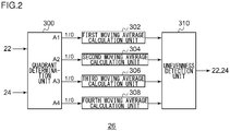
- Fig. 2 shows a configuration of the distribution detection unit 26.
- the distribution detection unit 26 includes a quadrant determination unit 300, a first moving average calculation unit 302, a second moving average calculation unit 304, a third moving average calculation unit 306, a fourth moving average calculation unit 308, and an unevenness detection unit 310.
- the quadrant determination unit 300 defines a plurality of quadrants as shown in Fig. 3 to determine the quadrant of the I signal from the first HPF 22 and the Q signal from the second HPF 24.
- Fig. 3 shows a plurality of quadrants defined by the quadrant determination unit 300. As illustrated, four quadrants A1, A2, A3, and A4 are defined. Denoting the value of the input I signal by "I” and denoting the value of input Q signal by "Q", the quadrant determination unit 300 groups the values in one of the quadrants A1, A2, A3, and A4 in accordance with the following conditions for determination.
- the quadrant determination unit 300 has output terminals corresponding to the four quadrants, respectively.
- the quadrant determination unit 300 outputs "1" from the output terminal corresponding to the quadrant in which the combination of the I signal and the Q signal is included and outputs "0" from the other output terminals.
- the first moving average calculation unit 302 is connected to the output terminal of the quadrant determination unit 300 corresponding to the quadrant "A1", and the second moving average calculation unit 304 is connected to the output terminal of the quadrant determination unit 300 corresponding to the quadrant "A2". Further, the third moving average calculation unit 306 is connected to the output terminal of the quadrant determination unit 300 corresponding to the quadrant "A3”, and the fourth moving average calculation unit 308 is connected to the output terminal of the quadrant determination unit 300 corresponding to the quadrant "A4". Each of the first moving average calculation unit 302 through the fourth moving average calculation unit 308 calculates a moving average of a predetermined number of samples of the values input from the quadrant determination unit 300. Each of the first moving average calculation unit 302 through the fourth moving average calculation unit 308 outputs the moving average value to the unevenness detection unit 310.
- the unevenness detection unit 310 receives the moving average value from each of the first moving average calculation unit 302 through the fourth moving average calculation unit 308. When the I signal and the Q signal occur in all quadrants in the predetermined number of samples, all moving average values will be other than "0". When the I signal and the Q signal do not occur in one of the quadrants, the moving average value corresponding to that quadrant will be "0". When any of the four moving average values becomes "0", the unevenness detection unit 310 outputs a detection signal, which indicates detection of an unevenness in the distribution, to the first HPF 22 and the second HPF 24.
- Fig. 4 shows another configuration of the distribution detection unit 26.
- the distribution detection unit 26 includes a quadrant determination unit 500, a power calculation unit 502, a selection unit 504, a first averaging unit 506, a second averaging unit 508, a third averaging unit 510, a fourth averaging unit 512, and a power comparison unit 514.
- the quadrant determination unit 500 performs a process similar to that of the quadrant determination unit 300.
- the quadrant determination unit 500 outputs the determined quadrant to the selection unit 504.
- the power calculation unit 502 receives the I signal from the first HPF 22 and the Q signal from the second HPF 24.
- the power calculation unit 502 calculates a square value of the I signal, calculates a square value of the Q signal, and calculates a power value by adding the square values.
- the power calculation unit 502 outputs the power value to the selection unit 504.
- the selection unit 504 receives the power value from the power calculation unit 502 and receives the result of quadrant determination from the quadrant determination unit 500.
- the selection unit 504 has output terminals corresponding to the four quadrants, respectively, and outputs the power value from the output terminal corresponding to the result of quadrant determination. The power value is not output from the other output terminals.
- the first averaging unit 506, the second averaging unit 508, the third averaging unit 510, and the fourth averaging unit 512 calculate an average of the input power value (hereinafter, "average power value"). In other words, the average power value for each quadrant is derived.
- the power comparison unit 514 receives the average of the power value from each of the first averaging unit 506 through the fourth averaging unit 512.
- the power comparison unit 514 detects an unevenness in the distribution by comparing the average power values of the respective quadrants. When the ratio between the maximum value and the minimum value of the average power values is 10 or greater, for example, the power comparison unit 514 outputs a detection signal indicating detection of an unevenness in the distribution to the first HPF 22 and the second HPF 24. The ratio is not limited to "10".
- Fig. 5 shows a configuration of the first HPF 22.
- the first HPF 22 includes an adder unit 600, a delay unit 602, an adder unit 604, an amplifier unit 606, an amplifier unit 608, a delay unit 610, a selection unit 612, and an amplifier unit 614.
- the delay unit 602 delays the I signal from the first ADC 14 by one sample.
- the I signal delayed by one sample is input to the primary LPF formed by the adder unit 604, the amplifier unit 608, and the delay unit 610, and the primary LPF outputs the averaged I signal.
- the coefficient of the amplifier unit 608 is ⁇
- the gain of the primary LPF formed by the adder unit 604, the amplifier unit 608, and the delay unit 610 will be 1/(1- ⁇ ) so that the amplifier unit 606 applies (1- ⁇ ) gain correction on the averaged I signal.
- the adder unit 600 subtracts the I signal with the corrected gain from the I signal from the first ADC 14.
- the adder unit 600 outputs an addition result as the I signal with the reduced direct current component.
- ⁇ is a value equal to or smaller than 1, and the closer ⁇ to 1, the steeper the characteristics of the HPF.
- the amplifier unit 614 corrects the gain of the moving average value.
- the selection unit 612 rewrites the value in the delay unit 610 by the moving average value with the corrected gain.
- the gain of the primary LPF formed by the adder unit 604, the amplifier unit 608, and the delay unit 610 is 1/(1- ⁇ ), and the value in the delay unit 610 will also be 1/(1- ⁇ ) times the average value. Therefore, when the gain of the input moving average value is 1, the amplifier unit 614 performs multiplication by 1/(1- ⁇ ) so that the gain will be the same as the gain of the value in the delay unit 610.
- the second HPF 24 is also configured as shown in Fig. 5 and processes the Q signal instead of the I signal.
- the distribution detection unit 26 detects an unevenness in the distribution
- the values in the first HPF 22 and the second HPF 24 are rewritten by the values of the direct current components measured in the first measurement filter 18 and the second measurement filter 20, respectively.
- the unevenness in the distribution of the I signal and the Q signal output from the first HPF 22 and the second HPF 24 is reduced so that the distortion of the signal demodulated by the demodulation unit 28 is also reduced.
- Fig. 6 shows a waveform of a signal input to the first HPF 22.
- the level of the I signal increases at "T1" due to a variation in the direct current component.
- the level of the I signal remains constant until “T1", and the level of the I signal from "T1" also remains constant.
- Fig. 7 shows a waveform of a signal output from the first HPF 22 in the absence of determination in the distribution detection unit 26.
- the first HPF 22 operates simply as an HPF, the variation in the direct current component from "T1" is directly output, and the direct current component converges to "0" in accordance with the time constant of the first HPF 22.
- the processing delay in the first HPF 22 is assumed to be "0".
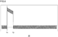
- Fig. 8 shows a waveform of a signal output from the first HPF 22.
- the distribution detection unit 26 determines that there is an unevenness in the signal after a predetermined period of time.
- the internal data in the first HPF 22 is replaced by the value of the I signal averaged by the first measurement filter 18 so that the signal as shown in Fig. 8 is output.
- the processing delay elapsed until the determination by the distribution detection unit 26 is denoted by "T2-T1" so that the level of the I signal from "T2" will be equal to the level of the I signal until "T1".
- the waveform of the signal in the second HPF 24 is also as shown in Fig. 6 through Fig. 8 .
- the features are implemented in hardware such as a CPU, a memory, or other LSI's, of any computer and in software such as a program loaded into a memory.
- the figure depicts functional blocks implemented by the cooperation of these elements. Therefore, it will be understood by those skilled in the art that the functional blocks may be implemented in a variety of manners by hardware only, software only, or by a combination of hardware and software.
- the status of the high-pass filter is changed when an unevenness in the distribution of the baseband signal is detected. Therefore, the impact of variation in the direct current component is reduced. Since the impact of variation in the direct current component is reduced, the time elapsed until the output is stabilized is reduced even in the presence of an abrupt variation in an unnecessary direct current component. Further, since the value of the signal in the high-pass filter is rewritten by the value of the direct current component when an unevenness in the distribution of the baseband signal is detected, the value is changed in such a manner the post-variation direct current component is cut.
- the variation in the output waveform of the high-pass filter caused by the variation in the direct current component is reduced. Since the variation in the output waveform of the high-pass filter caused by the variation in the direct current is reduced, the distortion in the waveform of the demodulated signal is reduced.
- Embodiment 2 of the present invention relates to direct conversion reception devices.
- Embodiment 2 is directed to the purpose of further reducing the period of time during which the signal output from the first HPF and the second HPF is subject to the impact of variation in the direct current component.
- the following description concerns a difference from the foregoing embodiment.
- Fig. 9 shows a configuration of a reception device 100 according to Embodiment 2.
- the reception device 100 includes a first delay circuit 32, a second delay circuit 34, a first detection HPF 36, and a second detection HPF 38.
- the first delay circuit 32 is provided between the first ADC 14 and the first HPF 22, and the second delay circuit 34 is provided between the second ADC 16 and the second HPF 24.
- the first HPF 22 is not connected to the distribution detection unit 26, but the first detection HPF 36 is connected to the first HPF 22.
- the second HPF 24 is not connected to the distribution detection unit 26, but the second detection HPF 38 is connected to the distribution detection unit 26.
- the first detection HPF 36 and the second detection HPF 38 have the same configuration as the first HPF 22 and the second HPF 24, respectively.
- the first delay circuit 32 delays the I signal output from the first ADC 14 over a period of time commensurate with the processing delay in the first measurement filter 18 and outputs the delayed I signal (hereinafter, also referred to as "I signal") to the first HPF 22.
- the second delay circuit 34 delays the Q signal output from the second ADC 16 over a period of time commensurate with the processing delay in the second measurement filter 20 and outputs the delayed Q signal (hereinafter, also referred to as "Q signal") to the second HPF 24.
- the first HPF 22 processes the I signal from the first delay circuit 32 as already described above
- the second HPF 24 processes the Q signal from the second delay circuit 34 as already described above.
- the first detection HPF 36 reduces the direct current component of the I signal from the first ADC 14 and outputs the I signal with the reduced direct current component (also referred to as "I signal") to the distribution detection unit 26.
- the I signal from the first ADC 14 can be said to be the I signal in which the delay induced by the first delay circuit 32 is avoided.
- the second detection HPF 38 reduces the direct current component of the Q signal from the second ADC 16 and outputs the Q signal with the reduced direct current component (also referred to as "Q signal”) to the distribution detection unit 26.
- the Q signal from the second ADC 16 can be said to be the Q signal in which the delay induced by the second delay circuit 34 is avoided.
- the distribution detection unit 26 processes the I signal from the first detection HPF 36 and the Q signal from the second detection HPF 38 as already described above.
- the distribution detection unit 26 detects an unevenness in the distribution, the distribution detection unit 26 rewrites the value of the signal in the first detection HPF 36 with the value of the direct current component measured in the first measurement filter 18. Further, when the distribution detection unit 26 detects an unevenness in the distribution, the distribution detection unit 26 rewrites the value of the signal in the second detection HPF 38 with the value of the direct current component measured in the second measurement filter 20.
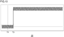
- Fig. 10 shows a waveform of a signal input to the first HPF 22.
- the I signal delayed by the first delay circuit 32 is input to the first HPF 22.
- the delay time induced by the first delay circuit 32 is denoted by "T3-T1".
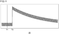
- Fig. 11 shows a waveform of a signal output from the first HPF 22 in the absence of determination in the distribution detection unit 26.
- the first HPF 22 operates simply as an HPF, the variation in the direct current component since "T3" is directly output, and the direct current component converges to "0" in accordance with the time constant of the first HPF 22.
- Fig. 12 shows a waveform of a signal output from the first HPF 22.
- the signal in the first HPF 22 is replaced by the value of the direct current component measured in the first measurement filter 18 so that the period of time subject to the impact from variation in the direct current component is further reduced.
- the baseband signal is delayed over a period of time commensurate with the processing delay in the measurement filter before outputting the baseband signal to the high-pass filter so that the timing of input of the baseband signal to the high-pass filter is delayed. Since the timing of input of the baseband signal to the high-pass filter is delayed, the period of time subject to the impact from variation in the direct current component is further reduced.
- Embodiment 3 also relates to direct conversion reception devices.
- Embodiment 3 is also directed to the purpose of further reducing the period of time subject to the impact from variation in the direct current component.
- the following description concerns a difference from the foregoing embodiments.
- the reception device 100 includes a delay device 60 and a muting unit (muting circuit) 62.
- the delay device 60 is connected to the demodulation unit 28 and receives the demodulated signal from the demodulation unit 28.
- the delay device 60 delays the demodulated signal and outputs the delayed demodulated signal (hereinafter, also referred to as "demodulated signal") to the muting unit 62.
- the muting unit 62 receives the demodulated signal from the delay device 60.
- the distribution detection unit 26 detects an unevenness in the distribution, the muting unit 62 mutes the demodulated signal. In other words, the muting unit 62 brings the demodulated signal to "0" over a certain period of time.
- Fig. 14 shows a waveform of a signal output from the demodulation unit 28. It is assumed that the waveform of the signal output from the first HPF 22 is identical to that of Fig. 8 .
- a pulse waveform may occur at "T1" and "T2".
- Fig. 15 shows a waveform of a signal output from the delay device 60.
- the delay induced by the delay device 60 shifts the pulse waveform occurring at "T1" to “T1'” and shifts the pulse waveform occurring at "T2" to "T2'".
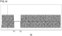
- Fig. 16 shows a waveform of a signal output from the muting unit 62.
- the muting unit 62 brings the pulse waveform occurring at "T1'" and "T2'" to "0".
- a distorted demodulated signal is output until the distribution detection unit detects an unevenness in the distribution.
- the distorted demodulated signal is delayed and muted so that the distorted demodulated signal is prevented from being output. Further, since the distorted demodulated signal is prevented from being output, the period of time subject to the impact from variation in the direct current component is further reduced.
- the time required until the output is stabilized is reduced even when an unnecessary direct current component varies abruptly.
Landscapes
- Engineering & Computer Science (AREA)
- Computer Networks & Wireless Communication (AREA)
- Signal Processing (AREA)
- Power Engineering (AREA)
- Noise Elimination (AREA)
- Circuits Of Receivers In General (AREA)
Claims (4)
- Eine Empfangsvorrichtung (100), aufweisend:einen Orthogonaldetektor (12), der konfiguriert ist zum Durchführen einer orthogonalen Erfassung auf einem empfangenen Signal, um ein I-Phase-Basisbandsignal und ein Q-Phase-Basisbandsignal, die orthogonal zueinander sind, auszugeben,Hochpassfilter (22, 24), die konfiguriert sind zum Reduzieren einer Gleichstromkomponente der entsprechenden aus dem Orthogonaldetektor (12) ausgegebenen Basisbandsignale,einen Demodulator (28), der konfiguriert ist zum Demodulieren der von den Hochpassfiltern (22, 24) ausgegebenen Basisbandsignale,einen Verteilungsdetektor (26), der konfiguriert ist zum Ableiten eines durchschnittlichen Leistungswerts des Basisbandsignals für jeden Quadranten einer IQ-Ebene, Vergleichen der durchschnittlichen Leistungswerte der entsprechenden Quadranten und Ausgeben eines Erfassungssignals, wenn das Vergleichsergebnis einen vorbestimmten Schwellwert überschreitet,Messfilter (18, 20), die konfiguriert sind zum Messen der Gleichstromkomponente der entsprechenden von dem Orthogonaldetektor (12) ausgegebenen Basisbandsignale,Verzögerungsschaltungen (32, 34), die konfiguriert sind zum Verzögern der entsprechenden von dem Orthogonaldetektor (12) ausgegebenen Basisbandsignale über eine Zeitperiode in Entsprechung zu einer Verarbeitungsverzögerung in den entsprechenden Messfiltern (18, 20), um die entsprechenden derart verzögerten Basisbandsignale zu den entsprechenden Hochpassfiltern (22, 24) auszugeben, undErfassungs-Hochpassfilter (36, 38), die konfiguriert sind zum Reduzieren der Gleichstromkomponente von entsprechenden von dem Orthogonaldetektor (12) ausgegebenen Basisbandsignalen und zum Ausgeben der entsprechenden Basisbandsignale mit der reduzierten Gleichstromkomponente an den Verteilungsdetektor (26),wobei der Verteilungsdetektor (26) das Erfassungssignal ausgibt, wobei der Erfassungsdetektor (26) konfiguriert ist zum Neuschreiben eines entsprechenden Werts eines Signals in den Hochpassfiltern (22, 24) und Erfassungs-Hochpassfiltern (36, 38) zu einem Wert der durch die Messfilter (18, 20) gemessenen Gleichstromkomponente.
- Empfangsvorrichtung (100) nach Anspruch 1, die weiterhin umfasst:
eine Ausblendungsschaltung (62), die konfiguriert ist zum Ausblenden eines von dem Demodulator (28) ausgegebenen Signals, wenn der Verteilungsdetektor (26) das Erfassungssignal ausgibt. - Ein Empfangsverfahren, aufweisend:Durchführen einer orthogonalen Erfassung auf einem empfangenen Signal, um ein erstes I-Phase-Basisbandsignal und ein erstes Q-Phase-Basisbandsignal, die orthogonal zueinander sind, auszugeben,Reduzieren einer Gleichstromkomponente jedes der ersten Basisbandsignale unter Verwendung von entsprechenden Erfassungs-Hochpassfiltern (36, 38), um dadurch zweite Basisbandsignale zu generieren,Ableiten eines durchschnittlichen Leistungswerts der zweiten Basisbandsignale für jeden Quadranten einer IQ-Ebene, Vergleichen der durchschnittlichen Leistungswerte der entsprechenden Quadranten und Ausgeben eines Erfassungssignals, wenn das Vergleichsergebnis einen vorbestimmten Schwellwert überschreitet,Messen der Gleichstromkomponente der entsprechenden aus der Orthogonalerfassung ausgegebenen ersten Basisbandsignale,Verzögern der entsprechenden von der Orthogonalerfassung ausgegebenen ersten Basisbandsignale über eine Zeitperiode in Entsprechung zu einer Verarbeitungsverzögerung in der entsprechenden Messung, um die entsprechenden derart verzögerten ersten Basisbandsignale an entsprechende Hochpassfilter (22, 24) auszugeben,Reduzieren der Gleichstromkomponente jedes der verzögerten ersten Basisbandsignale unter Verwendung von Hochpassfiltern (22, 24), um dadurch dritte Basisbandsignale zu generieren,Demodulieren jedes der dritten Basisbandsignale mit der reduzierten Gleichstromkomponente, undwenn das Erfassungssignal ausgegeben wird, Neuschreiben eines Werts eines Signals in den Hochpassfiltern (22, 24) und den Erfassungs-Hochpassfiltern (36, 38) zu einem Wert der durch die Messung gemessenen Gleichstromkomponente.
- Ein computerlesbares Speichermedium, das Befehle aufweist, die bei einer Ausführung durch einen Computer veranlassen, dass der Computer das Verfahren von Anspruch 3 durchführt.
Applications Claiming Priority (2)
| Application Number | Priority Date | Filing Date | Title |
|---|---|---|---|
| JP2017018466A JP6812816B2 (ja) | 2017-02-03 | 2017-02-03 | 受信装置、受信方法、プログラム |
| PCT/JP2017/043261 WO2018142745A1 (ja) | 2017-02-03 | 2017-12-01 | 受信装置、受信方法、プログラム |
Publications (4)
| Publication Number | Publication Date |
|---|---|
| EP3579433A1 EP3579433A1 (de) | 2019-12-11 |
| EP3579433A4 EP3579433A4 (de) | 2019-12-25 |
| EP3579433B1 true EP3579433B1 (de) | 2021-07-14 |
| EP3579433B8 EP3579433B8 (de) | 2021-08-18 |
Family
ID=63040534
Family Applications (1)
| Application Number | Title | Priority Date | Filing Date |
|---|---|---|---|
| EP17894732.1A Active EP3579433B8 (de) | 2017-02-03 | 2017-12-01 | Empfangsvorrichtung, empfangsverfahren und programm |
Country Status (4)
| Country | Link |
|---|---|
| US (1) | US10581653B2 (de) |
| EP (1) | EP3579433B8 (de) |
| JP (1) | JP6812816B2 (de) |
| WO (1) | WO2018142745A1 (de) |
Families Citing this family (2)
| Publication number | Priority date | Publication date | Assignee | Title |
|---|---|---|---|---|
| JP7056611B2 (ja) * | 2019-02-27 | 2022-04-19 | 株式会社Jvcケンウッド | 受信装置、プログラム |
| US11900961B2 (en) * | 2022-05-31 | 2024-02-13 | Microsoft Technology Licensing, Llc | Multichannel audio speech classification |
Family Cites Families (12)
| Publication number | Priority date | Publication date | Assignee | Title |
|---|---|---|---|---|
| US4969207A (en) * | 1987-03-20 | 1990-11-06 | Nippon Telegraph And Telephone Corporation | Radio receiver with reception deterioration compensation |
| JPH082058B2 (ja) | 1989-06-13 | 1996-01-10 | 日本電気株式会社 | 自動利得制御方式 |
| JPH04310037A (ja) * | 1991-04-09 | 1992-11-02 | Nec Corp | Fsk受信機 |
| DE69921475T2 (de) * | 1999-03-11 | 2006-02-02 | Mitsubishi Denki K.K. | Funkendgerät |
| JP3548148B2 (ja) * | 2001-09-27 | 2004-07-28 | 松下電器産業株式会社 | Ofdm送信装置及びofdm送信方法 |
| JP3805258B2 (ja) * | 2002-01-29 | 2006-08-02 | 松下電器産業株式会社 | ダイレクトコンバージョン受信機 |
| JP2013016878A (ja) * | 2009-11-04 | 2013-01-24 | Panasonic Corp | 受信装置及び受信方法 |
| US8638883B2 (en) * | 2010-02-03 | 2014-01-28 | Marvell World Trade Ltd. | DC offset cancellation in direct conversion receivers |
| JP2013120957A (ja) * | 2011-12-06 | 2013-06-17 | Toshiba Corp | 半導体集積回路、および、受信機 |
| US8811538B1 (en) * | 2013-03-15 | 2014-08-19 | Blackberry Limited | IQ error correction |
| WO2016121232A1 (ja) * | 2015-01-26 | 2016-08-04 | 株式会社Jvcケンウッド | Fm受信装置、fm受信方法 |
| WO2016136039A1 (ja) * | 2015-02-23 | 2016-09-01 | 株式会社Jvcケンウッド | Fm受信装置、fm受信方法 |
-
2017
- 2017-02-03 JP JP2017018466A patent/JP6812816B2/ja active Active
- 2017-12-01 WO PCT/JP2017/043261 patent/WO2018142745A1/ja not_active Ceased
- 2017-12-01 EP EP17894732.1A patent/EP3579433B8/de active Active
-
2019
- 2019-08-02 US US16/529,835 patent/US10581653B2/en active Active
Non-Patent Citations (1)
| Title |
|---|
| None * |
Also Published As
| Publication number | Publication date |
|---|---|
| WO2018142745A1 (ja) | 2018-08-09 |
| US10581653B2 (en) | 2020-03-03 |
| EP3579433B8 (de) | 2021-08-18 |
| US20190356521A1 (en) | 2019-11-21 |
| JP6812816B2 (ja) | 2021-01-13 |
| EP3579433A4 (de) | 2019-12-25 |
| EP3579433A1 (de) | 2019-12-11 |
| JP2018125794A (ja) | 2018-08-09 |
Similar Documents
| Publication | Publication Date | Title |
|---|---|---|
| US9118294B2 (en) | Receiving device and gain control method | |
| US9461681B1 (en) | Receiver | |
| US8804882B2 (en) | Receiving apparatus, and computer readable memory medium that stores a program | |
| US20090156143A1 (en) | Power control loop, transmitter with the power control loop and method for controlling output power of a transmitter device | |
| US20210234736A1 (en) | Receiver circuits with blocker attenuating mixer | |
| US9391814B2 (en) | FM receiver that receives FM signal and method for receiving FM signal | |
| US10581653B2 (en) | Reception device, reception method, recording medium for receiving signals | |
| JP5935631B2 (ja) | 補償装置及び無線通信装置 | |
| US10270483B2 (en) | FM reception device, FM reception method for receiving FM signals | |
| US20100074384A1 (en) | Receiving device, receiving method, and program | |
| US9461587B2 (en) | FM receiver that receives fm signal and method for receiving FM signal | |
| JP7060069B2 (ja) | 直流成分変動抑制装置、直流成分変動抑制方法、プログラム | |
| US10122395B2 (en) | FM reception device, FM reception method for receiving FM signals | |
| US9503296B2 (en) | FM receiver and FM receiving method for receiving FM signal | |
| JP2013124993A (ja) | レーダ受信機及びレーダ装置 | |
| JP7056611B2 (ja) | 受信装置、プログラム | |
| CN107276604B (zh) | 用于处理射频(rf)信号的方法和系统 | |
| JP6237309B2 (ja) | Fm受信装置、fm受信方法 | |
| WO2011055495A1 (ja) | 受信装置及び受信方法 | |
| JP4927054B2 (ja) | Fm信号のノイズキャンセラ回路 | |
| JP2015154242A (ja) | Fm受信装置、fm受信方法 | |
| JP2010147632A (ja) | 無線中継装置 | |
| JP2013179442A (ja) | アナログフィードバック増幅器およびアナログフィードバック制御方法 | |
| JP2010081389A (ja) | Fm信号のノイズキャンセラ回路 |
Legal Events
| Date | Code | Title | Description |
|---|---|---|---|
| STAA | Information on the status of an ep patent application or granted ep patent |
Free format text: STATUS: THE INTERNATIONAL PUBLICATION HAS BEEN MADE |
|
| PUAI | Public reference made under article 153(3) epc to a published international application that has entered the european phase |
Free format text: ORIGINAL CODE: 0009012 |
|
| STAA | Information on the status of an ep patent application or granted ep patent |
Free format text: STATUS: REQUEST FOR EXAMINATION WAS MADE |
|
| 17P | Request for examination filed |
Effective date: 20190730 |
|
| AK | Designated contracting states |
Kind code of ref document: A1 Designated state(s): AL AT BE BG CH CY CZ DE DK EE ES FI FR GB GR HR HU IE IS IT LI LT LU LV MC MK MT NL NO PL PT RO RS SE SI SK SM TR |
|
| AX | Request for extension of the european patent |
Extension state: BA ME |
|
| A4 | Supplementary search report drawn up and despatched |
Effective date: 20191121 |
|
| RIC1 | Information provided on ipc code assigned before grant |
Ipc: H04B 1/16 20060101ALI20191115BHEP Ipc: H03D 3/00 20060101ALI20191115BHEP Ipc: H04B 1/30 20060101AFI20191115BHEP Ipc: H04L 27/14 20060101ALI20191115BHEP |
|
| DAV | Request for validation of the european patent (deleted) | ||
| DAX | Request for extension of the european patent (deleted) | ||
| STAA | Information on the status of an ep patent application or granted ep patent |
Free format text: STATUS: EXAMINATION IS IN PROGRESS |
|
| 17Q | First examination report despatched |
Effective date: 20200716 |
|
| GRAP | Despatch of communication of intention to grant a patent |
Free format text: ORIGINAL CODE: EPIDOSNIGR1 |
|
| STAA | Information on the status of an ep patent application or granted ep patent |
Free format text: STATUS: GRANT OF PATENT IS INTENDED |
|
| INTG | Intention to grant announced |
Effective date: 20210218 |
|
| GRAS | Grant fee paid |
Free format text: ORIGINAL CODE: EPIDOSNIGR3 |
|
| GRAA | (expected) grant |
Free format text: ORIGINAL CODE: 0009210 |
|
| STAA | Information on the status of an ep patent application or granted ep patent |
Free format text: STATUS: THE PATENT HAS BEEN GRANTED |
|
| AK | Designated contracting states |
Kind code of ref document: B1 Designated state(s): AL AT BE BG CH CY CZ DE DK EE ES FI FR GB GR HR HU IE IS IT LI LT LU LV MC MK MT NL NO PL PT RO RS SE SI SK SM TR |
|
| REG | Reference to a national code |
Ref country code: GB Ref legal event code: FG4D |
|
| REG | Reference to a national code |
Ref country code: DE Ref legal event code: R081 Ref document number: 602017042313 Country of ref document: DE Owner name: JVCKENWOOD CORPORATION, YOKOHAMA-SHI, JP Free format text: FORMER OWNER: JVC KENWOOD CORPORATION, YOKOHAMA-SHI, KANAGAWA, JP |
|
| REG | Reference to a national code |
Ref country code: CH Ref legal event code: PK Free format text: BERICHTIGUNG B8 |
|
| REG | Reference to a national code |
Ref country code: IE Ref legal event code: FG4D |
|
| REG | Reference to a national code |
Ref country code: DE Ref legal event code: R096 Ref document number: 602017042313 Country of ref document: DE |
|
| RAP4 | Party data changed (patent owner data changed or rights of a patent transferred) |
Owner name: JVCKENWOOD CORPORATION |
|
| REG | Reference to a national code |
Ref country code: AT Ref legal event code: REF Ref document number: 1411453 Country of ref document: AT Kind code of ref document: T Effective date: 20210815 |
|
| REG | Reference to a national code |
Ref country code: LT Ref legal event code: MG9D |
|
| REG | Reference to a national code |
Ref country code: NL Ref legal event code: MP Effective date: 20210714 |
|
| REG | Reference to a national code |
Ref country code: AT Ref legal event code: MK05 Ref document number: 1411453 Country of ref document: AT Kind code of ref document: T Effective date: 20210714 |
|
| PG25 | Lapsed in a contracting state [announced via postgrant information from national office to epo] |
Ref country code: NL Free format text: LAPSE BECAUSE OF FAILURE TO SUBMIT A TRANSLATION OF THE DESCRIPTION OR TO PAY THE FEE WITHIN THE PRESCRIBED TIME-LIMIT Effective date: 20210714 Ref country code: NO Free format text: LAPSE BECAUSE OF FAILURE TO SUBMIT A TRANSLATION OF THE DESCRIPTION OR TO PAY THE FEE WITHIN THE PRESCRIBED TIME-LIMIT Effective date: 20211014 Ref country code: PT Free format text: LAPSE BECAUSE OF FAILURE TO SUBMIT A TRANSLATION OF THE DESCRIPTION OR TO PAY THE FEE WITHIN THE PRESCRIBED TIME-LIMIT Effective date: 20211115 Ref country code: LT Free format text: LAPSE BECAUSE OF FAILURE TO SUBMIT A TRANSLATION OF THE DESCRIPTION OR TO PAY THE FEE WITHIN THE PRESCRIBED TIME-LIMIT Effective date: 20210714 Ref country code: AT Free format text: LAPSE BECAUSE OF FAILURE TO SUBMIT A TRANSLATION OF THE DESCRIPTION OR TO PAY THE FEE WITHIN THE PRESCRIBED TIME-LIMIT Effective date: 20210714 Ref country code: BG Free format text: LAPSE BECAUSE OF FAILURE TO SUBMIT A TRANSLATION OF THE DESCRIPTION OR TO PAY THE FEE WITHIN THE PRESCRIBED TIME-LIMIT Effective date: 20211014 Ref country code: SE Free format text: LAPSE BECAUSE OF FAILURE TO SUBMIT A TRANSLATION OF THE DESCRIPTION OR TO PAY THE FEE WITHIN THE PRESCRIBED TIME-LIMIT Effective date: 20210714 Ref country code: RS Free format text: LAPSE BECAUSE OF FAILURE TO SUBMIT A TRANSLATION OF THE DESCRIPTION OR TO PAY THE FEE WITHIN THE PRESCRIBED TIME-LIMIT Effective date: 20210714 Ref country code: ES Free format text: LAPSE BECAUSE OF FAILURE TO SUBMIT A TRANSLATION OF THE DESCRIPTION OR TO PAY THE FEE WITHIN THE PRESCRIBED TIME-LIMIT Effective date: 20210714 Ref country code: FI Free format text: LAPSE BECAUSE OF FAILURE TO SUBMIT A TRANSLATION OF THE DESCRIPTION OR TO PAY THE FEE WITHIN THE PRESCRIBED TIME-LIMIT Effective date: 20210714 Ref country code: HR Free format text: LAPSE BECAUSE OF FAILURE TO SUBMIT A TRANSLATION OF THE DESCRIPTION OR TO PAY THE FEE WITHIN THE PRESCRIBED TIME-LIMIT Effective date: 20210714 |
|
| PG25 | Lapsed in a contracting state [announced via postgrant information from national office to epo] |
Ref country code: PL Free format text: LAPSE BECAUSE OF FAILURE TO SUBMIT A TRANSLATION OF THE DESCRIPTION OR TO PAY THE FEE WITHIN THE PRESCRIBED TIME-LIMIT Effective date: 20210714 Ref country code: LV Free format text: LAPSE BECAUSE OF FAILURE TO SUBMIT A TRANSLATION OF THE DESCRIPTION OR TO PAY THE FEE WITHIN THE PRESCRIBED TIME-LIMIT Effective date: 20210714 Ref country code: GR Free format text: LAPSE BECAUSE OF FAILURE TO SUBMIT A TRANSLATION OF THE DESCRIPTION OR TO PAY THE FEE WITHIN THE PRESCRIBED TIME-LIMIT Effective date: 20211015 |
|
| REG | Reference to a national code |
Ref country code: DE Ref legal event code: R097 Ref document number: 602017042313 Country of ref document: DE |
|
| PG25 | Lapsed in a contracting state [announced via postgrant information from national office to epo] |
Ref country code: DK Free format text: LAPSE BECAUSE OF FAILURE TO SUBMIT A TRANSLATION OF THE DESCRIPTION OR TO PAY THE FEE WITHIN THE PRESCRIBED TIME-LIMIT Effective date: 20210714 |
|
| PLBE | No opposition filed within time limit |
Free format text: ORIGINAL CODE: 0009261 |
|
| STAA | Information on the status of an ep patent application or granted ep patent |
Free format text: STATUS: NO OPPOSITION FILED WITHIN TIME LIMIT |
|
| PG25 | Lapsed in a contracting state [announced via postgrant information from national office to epo] |
Ref country code: SM Free format text: LAPSE BECAUSE OF FAILURE TO SUBMIT A TRANSLATION OF THE DESCRIPTION OR TO PAY THE FEE WITHIN THE PRESCRIBED TIME-LIMIT Effective date: 20210714 Ref country code: SK Free format text: LAPSE BECAUSE OF FAILURE TO SUBMIT A TRANSLATION OF THE DESCRIPTION OR TO PAY THE FEE WITHIN THE PRESCRIBED TIME-LIMIT Effective date: 20210714 Ref country code: RO Free format text: LAPSE BECAUSE OF FAILURE TO SUBMIT A TRANSLATION OF THE DESCRIPTION OR TO PAY THE FEE WITHIN THE PRESCRIBED TIME-LIMIT Effective date: 20210714 Ref country code: EE Free format text: LAPSE BECAUSE OF FAILURE TO SUBMIT A TRANSLATION OF THE DESCRIPTION OR TO PAY THE FEE WITHIN THE PRESCRIBED TIME-LIMIT Effective date: 20210714 Ref country code: CZ Free format text: LAPSE BECAUSE OF FAILURE TO SUBMIT A TRANSLATION OF THE DESCRIPTION OR TO PAY THE FEE WITHIN THE PRESCRIBED TIME-LIMIT Effective date: 20210714 Ref country code: AL Free format text: LAPSE BECAUSE OF FAILURE TO SUBMIT A TRANSLATION OF THE DESCRIPTION OR TO PAY THE FEE WITHIN THE PRESCRIBED TIME-LIMIT Effective date: 20210714 |
|
| 26N | No opposition filed |
Effective date: 20220419 |
|
| PG25 | Lapsed in a contracting state [announced via postgrant information from national office to epo] |
Ref country code: MC Free format text: LAPSE BECAUSE OF FAILURE TO SUBMIT A TRANSLATION OF THE DESCRIPTION OR TO PAY THE FEE WITHIN THE PRESCRIBED TIME-LIMIT Effective date: 20210714 Ref country code: IT Free format text: LAPSE BECAUSE OF FAILURE TO SUBMIT A TRANSLATION OF THE DESCRIPTION OR TO PAY THE FEE WITHIN THE PRESCRIBED TIME-LIMIT Effective date: 20210714 |
|
| REG | Reference to a national code |
Ref country code: CH Ref legal event code: PL |
|
| REG | Reference to a national code |
Ref country code: BE Ref legal event code: MM Effective date: 20211231 |
|
| PG25 | Lapsed in a contracting state [announced via postgrant information from national office to epo] |
Ref country code: LU Free format text: LAPSE BECAUSE OF NON-PAYMENT OF DUE FEES Effective date: 20211201 Ref country code: IE Free format text: LAPSE BECAUSE OF NON-PAYMENT OF DUE FEES Effective date: 20211201 |
|
| PG25 | Lapsed in a contracting state [announced via postgrant information from national office to epo] |
Ref country code: BE Free format text: LAPSE BECAUSE OF NON-PAYMENT OF DUE FEES Effective date: 20211231 |
|
| PG25 | Lapsed in a contracting state [announced via postgrant information from national office to epo] |
Ref country code: LI Free format text: LAPSE BECAUSE OF NON-PAYMENT OF DUE FEES Effective date: 20211231 Ref country code: CH Free format text: LAPSE BECAUSE OF NON-PAYMENT OF DUE FEES Effective date: 20211231 |
|
| PG25 | Lapsed in a contracting state [announced via postgrant information from national office to epo] |
Ref country code: CY Free format text: LAPSE BECAUSE OF FAILURE TO SUBMIT A TRANSLATION OF THE DESCRIPTION OR TO PAY THE FEE WITHIN THE PRESCRIBED TIME-LIMIT Effective date: 20210714 |
|
| PG25 | Lapsed in a contracting state [announced via postgrant information from national office to epo] |
Ref country code: HU Free format text: LAPSE BECAUSE OF FAILURE TO SUBMIT A TRANSLATION OF THE DESCRIPTION OR TO PAY THE FEE WITHIN THE PRESCRIBED TIME-LIMIT; INVALID AB INITIO Effective date: 20171201 |
|
| PG25 | Lapsed in a contracting state [announced via postgrant information from national office to epo] |
Ref country code: MK Free format text: LAPSE BECAUSE OF FAILURE TO SUBMIT A TRANSLATION OF THE DESCRIPTION OR TO PAY THE FEE WITHIN THE PRESCRIBED TIME-LIMIT Effective date: 20210714 |
|
| PG25 | Lapsed in a contracting state [announced via postgrant information from national office to epo] |
Ref country code: TR Free format text: LAPSE BECAUSE OF FAILURE TO SUBMIT A TRANSLATION OF THE DESCRIPTION OR TO PAY THE FEE WITHIN THE PRESCRIBED TIME-LIMIT Effective date: 20210714 |
|
| PG25 | Lapsed in a contracting state [announced via postgrant information from national office to epo] |
Ref country code: MT Free format text: LAPSE BECAUSE OF FAILURE TO SUBMIT A TRANSLATION OF THE DESCRIPTION OR TO PAY THE FEE WITHIN THE PRESCRIBED TIME-LIMIT Effective date: 20210714 |
|
| PGFP | Annual fee paid to national office [announced via postgrant information from national office to epo] |
Ref country code: DE Payment date: 20251028 Year of fee payment: 9 |
|
| PGFP | Annual fee paid to national office [announced via postgrant information from national office to epo] |
Ref country code: GB Payment date: 20251030 Year of fee payment: 9 |
|
| PGFP | Annual fee paid to national office [announced via postgrant information from national office to epo] |
Ref country code: FR Payment date: 20251117 Year of fee payment: 9 |