EP3576286A1 - Vorrichtung zur steuerung eines wechselrichters - Google Patents
Vorrichtung zur steuerung eines wechselrichters Download PDFInfo
- Publication number
- EP3576286A1 EP3576286A1 EP19161447.8A EP19161447A EP3576286A1 EP 3576286 A1 EP3576286 A1 EP 3576286A1 EP 19161447 A EP19161447 A EP 19161447A EP 3576286 A1 EP3576286 A1 EP 3576286A1
- Authority
- EP
- European Patent Office
- Prior art keywords
- phase
- voltage
- command
- command voltage
- difference
- Prior art date
- Legal status (The legal status is an assumption and is not a legal conclusion. Google has not performed a legal analysis and makes no representation as to the accuracy of the status listed.)
- Withdrawn
Links
- 230000001131 transforming effect Effects 0.000 claims abstract description 9
- 239000013598 vector Substances 0.000 description 41
- 238000010586 diagram Methods 0.000 description 14
- 230000009466 transformation Effects 0.000 description 6
- 238000000034 method Methods 0.000 description 5
- 238000005516 engineering process Methods 0.000 description 4
- 238000007796 conventional method Methods 0.000 description 3
- 238000004146 energy storage Methods 0.000 description 3
- 230000015572 biosynthetic process Effects 0.000 description 2
- 230000008859 change Effects 0.000 description 2
- 238000006243 chemical reaction Methods 0.000 description 2
- 230000000694 effects Effects 0.000 description 2
- 238000012986 modification Methods 0.000 description 2
- 230000004048 modification Effects 0.000 description 2
- 239000004065 semiconductor Substances 0.000 description 2
- 238000003786 synthesis reaction Methods 0.000 description 2
- 230000000295 complement effect Effects 0.000 description 1
- 230000007935 neutral effect Effects 0.000 description 1
- 230000008569 process Effects 0.000 description 1
Images




Classifications
-
- H—ELECTRICITY
- H02—GENERATION; CONVERSION OR DISTRIBUTION OF ELECTRIC POWER
- H02M—APPARATUS FOR CONVERSION BETWEEN AC AND AC, BETWEEN AC AND DC, OR BETWEEN DC AND DC, AND FOR USE WITH MAINS OR SIMILAR POWER SUPPLY SYSTEMS; CONVERSION OF DC OR AC INPUT POWER INTO SURGE OUTPUT POWER; CONTROL OR REGULATION THEREOF
- H02M7/00—Conversion of AC power input into DC power output; Conversion of DC power input into AC power output
- H02M7/42—Conversion of DC power input into AC power output without possibility of reversal
- H02M7/44—Conversion of DC power input into AC power output without possibility of reversal by static converters
- H02M7/48—Conversion of DC power input into AC power output without possibility of reversal by static converters using discharge tubes with control electrode or semiconductor devices with control electrode
- H02M7/53—Conversion of DC power input into AC power output without possibility of reversal by static converters using discharge tubes with control electrode or semiconductor devices with control electrode using devices of a triode or transistor type requiring continuous application of a control signal
- H02M7/537—Conversion of DC power input into AC power output without possibility of reversal by static converters using discharge tubes with control electrode or semiconductor devices with control electrode using devices of a triode or transistor type requiring continuous application of a control signal using semiconductor devices only, e.g. single switched pulse inverters
- H02M7/5387—Conversion of DC power input into AC power output without possibility of reversal by static converters using discharge tubes with control electrode or semiconductor devices with control electrode using devices of a triode or transistor type requiring continuous application of a control signal using semiconductor devices only, e.g. single switched pulse inverters in a bridge configuration
-
- H—ELECTRICITY
- H02—GENERATION; CONVERSION OR DISTRIBUTION OF ELECTRIC POWER
- H02M—APPARATUS FOR CONVERSION BETWEEN AC AND AC, BETWEEN AC AND DC, OR BETWEEN DC AND DC, AND FOR USE WITH MAINS OR SIMILAR POWER SUPPLY SYSTEMS; CONVERSION OF DC OR AC INPUT POWER INTO SURGE OUTPUT POWER; CONTROL OR REGULATION THEREOF
- H02M7/00—Conversion of AC power input into DC power output; Conversion of DC power input into AC power output
- H02M7/42—Conversion of DC power input into AC power output without possibility of reversal
- H02M7/44—Conversion of DC power input into AC power output without possibility of reversal by static converters
- H02M7/48—Conversion of DC power input into AC power output without possibility of reversal by static converters using discharge tubes with control electrode or semiconductor devices with control electrode
- H02M7/53—Conversion of DC power input into AC power output without possibility of reversal by static converters using discharge tubes with control electrode or semiconductor devices with control electrode using devices of a triode or transistor type requiring continuous application of a control signal
- H02M7/537—Conversion of DC power input into AC power output without possibility of reversal by static converters using discharge tubes with control electrode or semiconductor devices with control electrode using devices of a triode or transistor type requiring continuous application of a control signal using semiconductor devices only, e.g. single switched pulse inverters
- H02M7/539—Conversion of DC power input into AC power output without possibility of reversal by static converters using discharge tubes with control electrode or semiconductor devices with control electrode using devices of a triode or transistor type requiring continuous application of a control signal using semiconductor devices only, e.g. single switched pulse inverters with automatic control of output wave form or frequency
- H02M7/5395—Conversion of DC power input into AC power output without possibility of reversal by static converters using discharge tubes with control electrode or semiconductor devices with control electrode using devices of a triode or transistor type requiring continuous application of a control signal using semiconductor devices only, e.g. single switched pulse inverters with automatic control of output wave form or frequency by pulse-width modulation
-
- H—ELECTRICITY
- H02—GENERATION; CONVERSION OR DISTRIBUTION OF ELECTRIC POWER
- H02M—APPARATUS FOR CONVERSION BETWEEN AC AND AC, BETWEEN AC AND DC, OR BETWEEN DC AND DC, AND FOR USE WITH MAINS OR SIMILAR POWER SUPPLY SYSTEMS; CONVERSION OF DC OR AC INPUT POWER INTO SURGE OUTPUT POWER; CONTROL OR REGULATION THEREOF
- H02M1/00—Details of apparatus for conversion
- H02M1/08—Circuits specially adapted for the generation of control voltages for semiconductor devices incorporated in static converters
-
- H—ELECTRICITY
- H02—GENERATION; CONVERSION OR DISTRIBUTION OF ELECTRIC POWER
- H02M—APPARATUS FOR CONVERSION BETWEEN AC AND AC, BETWEEN AC AND DC, OR BETWEEN DC AND DC, AND FOR USE WITH MAINS OR SIMILAR POWER SUPPLY SYSTEMS; CONVERSION OF DC OR AC INPUT POWER INTO SURGE OUTPUT POWER; CONTROL OR REGULATION THEREOF
- H02M1/00—Details of apparatus for conversion
- H02M1/12—Arrangements for reducing harmonics from AC input or output
-
- H—ELECTRICITY
- H02—GENERATION; CONVERSION OR DISTRIBUTION OF ELECTRIC POWER
- H02M—APPARATUS FOR CONVERSION BETWEEN AC AND AC, BETWEEN AC AND DC, OR BETWEEN DC AND DC, AND FOR USE WITH MAINS OR SIMILAR POWER SUPPLY SYSTEMS; CONVERSION OF DC OR AC INPUT POWER INTO SURGE OUTPUT POWER; CONTROL OR REGULATION THEREOF
- H02M3/00—Conversion of DC power input into DC power output
- H02M3/22—Conversion of DC power input into DC power output with intermediate conversion into AC
- H02M3/24—Conversion of DC power input into DC power output with intermediate conversion into AC by static converters
- H02M3/28—Conversion of DC power input into DC power output with intermediate conversion into AC by static converters using discharge tubes with control electrode or semiconductor devices with control electrode to produce the intermediate AC
- H02M3/325—Conversion of DC power input into DC power output with intermediate conversion into AC by static converters using discharge tubes with control electrode or semiconductor devices with control electrode to produce the intermediate AC using devices of a triode or a transistor type requiring continuous application of a control signal
- H02M3/335—Conversion of DC power input into DC power output with intermediate conversion into AC by static converters using discharge tubes with control electrode or semiconductor devices with control electrode to produce the intermediate AC using devices of a triode or a transistor type requiring continuous application of a control signal using semiconductor devices only
-
- H—ELECTRICITY
- H02—GENERATION; CONVERSION OR DISTRIBUTION OF ELECTRIC POWER
- H02M—APPARATUS FOR CONVERSION BETWEEN AC AND AC, BETWEEN AC AND DC, OR BETWEEN DC AND DC, AND FOR USE WITH MAINS OR SIMILAR POWER SUPPLY SYSTEMS; CONVERSION OF DC OR AC INPUT POWER INTO SURGE OUTPUT POWER; CONTROL OR REGULATION THEREOF
- H02M7/00—Conversion of AC power input into DC power output; Conversion of DC power input into AC power output
- H02M7/42—Conversion of DC power input into AC power output without possibility of reversal
- H02M7/44—Conversion of DC power input into AC power output without possibility of reversal by static converters
- H02M7/48—Conversion of DC power input into AC power output without possibility of reversal by static converters using discharge tubes with control electrode or semiconductor devices with control electrode
-
- H—ELECTRICITY
- H02—GENERATION; CONVERSION OR DISTRIBUTION OF ELECTRIC POWER
- H02P—CONTROL OR REGULATION OF ELECTRIC MOTORS, ELECTRIC GENERATORS OR DYNAMO-ELECTRIC CONVERTERS; CONTROLLING TRANSFORMERS, REACTORS OR CHOKE COILS
- H02P21/00—Arrangements or methods for the control of electric machines by vector control, e.g. by control of field orientation
- H02P21/22—Current control, e.g. using a current control loop
-
- H—ELECTRICITY
- H02—GENERATION; CONVERSION OR DISTRIBUTION OF ELECTRIC POWER
- H02P—CONTROL OR REGULATION OF ELECTRIC MOTORS, ELECTRIC GENERATORS OR DYNAMO-ELECTRIC CONVERTERS; CONTROLLING TRANSFORMERS, REACTORS OR CHOKE COILS
- H02P27/00—Arrangements or methods for the control of AC motors characterised by the kind of supply voltage
- H02P27/04—Arrangements or methods for the control of AC motors characterised by the kind of supply voltage using variable-frequency supply voltage, e.g. inverter or converter supply voltage
- H02P27/06—Arrangements or methods for the control of AC motors characterised by the kind of supply voltage using variable-frequency supply voltage, e.g. inverter or converter supply voltage using DC to AC converters or inverters
- H02P27/08—Arrangements or methods for the control of AC motors characterised by the kind of supply voltage using variable-frequency supply voltage, e.g. inverter or converter supply voltage using DC to AC converters or inverters with pulse width modulation
-
- H—ELECTRICITY
- H02—GENERATION; CONVERSION OR DISTRIBUTION OF ELECTRIC POWER
- H02M—APPARATUS FOR CONVERSION BETWEEN AC AND AC, BETWEEN AC AND DC, OR BETWEEN DC AND DC, AND FOR USE WITH MAINS OR SIMILAR POWER SUPPLY SYSTEMS; CONVERSION OF DC OR AC INPUT POWER INTO SURGE OUTPUT POWER; CONTROL OR REGULATION THEREOF
- H02M1/00—Details of apparatus for conversion
- H02M1/0048—Circuits or arrangements for reducing losses
-
- H—ELECTRICITY
- H02—GENERATION; CONVERSION OR DISTRIBUTION OF ELECTRIC POWER
- H02M—APPARATUS FOR CONVERSION BETWEEN AC AND AC, BETWEEN AC AND DC, OR BETWEEN DC AND DC, AND FOR USE WITH MAINS OR SIMILAR POWER SUPPLY SYSTEMS; CONVERSION OF DC OR AC INPUT POWER INTO SURGE OUTPUT POWER; CONTROL OR REGULATION THEREOF
- H02M1/00—Details of apparatus for conversion
- H02M1/0048—Circuits or arrangements for reducing losses
- H02M1/0054—Transistor switching losses
-
- H—ELECTRICITY
- H02—GENERATION; CONVERSION OR DISTRIBUTION OF ELECTRIC POWER
- H02M—APPARATUS FOR CONVERSION BETWEEN AC AND AC, BETWEEN AC AND DC, OR BETWEEN DC AND DC, AND FOR USE WITH MAINS OR SIMILAR POWER SUPPLY SYSTEMS; CONVERSION OF DC OR AC INPUT POWER INTO SURGE OUTPUT POWER; CONTROL OR REGULATION THEREOF
- H02M7/00—Conversion of AC power input into DC power output; Conversion of DC power input into AC power output
- H02M7/42—Conversion of DC power input into AC power output without possibility of reversal
- H02M7/44—Conversion of DC power input into AC power output without possibility of reversal by static converters
- H02M7/48—Conversion of DC power input into AC power output without possibility of reversal by static converters using discharge tubes with control electrode or semiconductor devices with control electrode
- H02M7/53—Conversion of DC power input into AC power output without possibility of reversal by static converters using discharge tubes with control electrode or semiconductor devices with control electrode using devices of a triode or transistor type requiring continuous application of a control signal
- H02M7/537—Conversion of DC power input into AC power output without possibility of reversal by static converters using discharge tubes with control electrode or semiconductor devices with control electrode using devices of a triode or transistor type requiring continuous application of a control signal using semiconductor devices only, e.g. single switched pulse inverters
- H02M7/5387—Conversion of DC power input into AC power output without possibility of reversal by static converters using discharge tubes with control electrode or semiconductor devices with control electrode using devices of a triode or transistor type requiring continuous application of a control signal using semiconductor devices only, e.g. single switched pulse inverters in a bridge configuration
- H02M7/53871—Conversion of DC power input into AC power output without possibility of reversal by static converters using discharge tubes with control electrode or semiconductor devices with control electrode using devices of a triode or transistor type requiring continuous application of a control signal using semiconductor devices only, e.g. single switched pulse inverters in a bridge configuration with automatic control of output voltage or current
- H02M7/53875—Conversion of DC power input into AC power output without possibility of reversal by static converters using discharge tubes with control electrode or semiconductor devices with control electrode using devices of a triode or transistor type requiring continuous application of a control signal using semiconductor devices only, e.g. single switched pulse inverters in a bridge configuration with automatic control of output voltage or current with analogue control of three-phase output
-
- Y—GENERAL TAGGING OF NEW TECHNOLOGICAL DEVELOPMENTS; GENERAL TAGGING OF CROSS-SECTIONAL TECHNOLOGIES SPANNING OVER SEVERAL SECTIONS OF THE IPC; TECHNICAL SUBJECTS COVERED BY FORMER USPC CROSS-REFERENCE ART COLLECTIONS [XRACs] AND DIGESTS
- Y02—TECHNOLOGIES OR APPLICATIONS FOR MITIGATION OR ADAPTATION AGAINST CLIMATE CHANGE
- Y02B—CLIMATE CHANGE MITIGATION TECHNOLOGIES RELATED TO BUILDINGS, e.g. HOUSING, HOUSE APPLIANCES OR RELATED END-USER APPLICATIONS
- Y02B70/00—Technologies for an efficient end-user side electric power management and consumption
- Y02B70/10—Technologies improving the efficiency by using switched-mode power supplies [SMPS], i.e. efficient power electronics conversion e.g. power factor correction or reduction of losses in power supplies or efficient standby modes
Definitions
- the present disclosure relates to a device for controlling an inverter.
- VVVF Very Voltage and Variable Frequency
- An example of a circuit for generating the VVVF may include a voltage-type inverter which convert a DC voltage as an input to an AC variable voltage as an output.
- the voltage-type inverter may be mainly used in energy storage system (ESS), photo-voltaic (PV) inverter, and motor drive technology.
- ESS energy storage system
- PV photo-voltaic
- the pulse width modulation schemes includes a sinusoidal pulse width modulation (SPWM) and a space vector pulse width modulation (SVPWM).
- SPWM sinusoidal pulse width modulation
- SVPWM space vector pulse width modulation
- the above SPWM and SVPWM may belong to a continuous pulse width modulation scheme.
- a discontinuous pulse width modulation scheme is also used to reduce a switching loss in a power semiconductor.
- a 60° discontinuous pulse width modulation (DPWM) scheme is the most representative discontinuous pulse width modulation scheme.
- This discontinuous pulse width modulation scheme may be implemented by appropriately selecting an offset voltage in a pulse width modulation scheme using an offset voltage and a triangular carrier wave comparison PWM.
- the discontinuous pulse width modulation scheme may include a discontinuous pulse width modulation scheme of adjusting a discontinuous pulse width modulation period.
- This scheme may achieve an optimal current total harmonic distortion (THD) and loss at each operating point by freely adjusting a duration of the discontinuous pulse width modulation period.
- TDD current total harmonic distortion
- This scheme always has a minimum loss when a power factor is 1. Thus, it is necessary to have a minimum loss regardless of the power factor.
- the present disclosure aims to provide an inverter-controlling device which allows a user to control a trade-off between a switching loss and a current THD via adjustment of a discontinuous modulation duration, such that at a given discontinuous modulation duration, there is always a minimum loss regardless of a power factor.
- a device for controlling an inverter wherein the device achieves a minimum switching loss in a discontinuous modulation duration regardless of a power factor
- the inverter includes an inverting module for converting a direct current (DC) stage voltage to an alternate current (AC) voltage
- the inverting module includes 3 legs corresponding to 3 phases, wherein each leg has upper and lower switching elements
- the device being characterized in that the device includes: a command voltage transform unit configured for transforming each of 3 phases command voltages into each of pole command voltages using the DC stage voltage, a pulse width modulation index, a discontinuous modulation angle corresponding to a discontinuous modulation duration, and each phase difference between each of the 3 phase command voltages and each of 3 phases output currents of the inverting module; and a controller configured for generating a control signal based on a comparison between each pole command voltage and a triangular carrier wave, wherein the control signal controls upper and lower switching elements of each phase leg.
- the command voltage transform unit includes: an offset command voltage calculation unit for calculating an offset command voltage from the phase command voltages, the DC stage voltage, the pulse width modulation index, the discontinuous modulation angle, and each phase difference; and a pole command voltage calculation unit for calculating each pole command voltage from each phase command voltage and the offset command voltage.
- the offset command voltage calculation unit includes: a first coordinate transform unit for transforming the 3 phases command voltages to stationary reference frame-based d and q axis command voltages; an angular transform unit for transforming each phase-difference between each phase command voltage and each output current into each virtual phase-difference; a rotation transform unit for rotationally-transforming the stationary reference frame-based d and q axis command voltages by each virtual phase-difference; a second coordinate transform unit for transforming the rotation-transformed d and q axis command voltages into virtual 3-phases command voltages; and an offset command voltage generation unit for generating the offset command voltage using the phase command voltages, the DC stage voltage, the pulse width modulation index, the discontinuous modulation angle, and the virtual phase command voltages.
- the offset command voltage generation unit includes: a first determination unit for determining a maximum value and a minimum value among the actual 3 phases command voltages; a second determination unit for determining a maximum value and a minimum value among the virtual 3 phases command voltages; and a third determination unit for determining the offset command voltage using the DC stage voltage, the pulse width modulation index, the discontinuous modulation angle, the maximum and minimum values among the actual phase command voltages, and the maximum and minimum values among the virtual phase command voltages.
- v sn * denotes the offset command voltage
- V dc denotes the DC stage voltage
- k is defined as MIcos ⁇ D
- MI denotes the pulse width modulation index
- ⁇ D denotes the discontinuous modulation angle
- v max * and v min * denote the maximum and minimum values among the actual phase command voltages respectively
- the phase-difference ⁇ has a relationship 0 ⁇ ⁇ ⁇ ⁇ 3 ⁇ ⁇ D
- the phase-difference ⁇ has a relationship ⁇ 3 ⁇ ⁇ D ⁇ ⁇ ⁇ ⁇ 2 ⁇ ⁇ D
- the phase-difference ⁇ has a relationship ⁇ 2 ⁇ ⁇ D ⁇ ⁇ ⁇ ⁇ 2
- the controller includes: a comparison unit configured for: comparing each polar command voltage with a triangular carrier wave; when a difference between each polar command voltage and the triangular carrier wave is positive or zero, outputting 1 as a switching function of an upper switching element of each leg; or when a difference between each polar command voltage and the triangular carrier wave is negative, outputting 0 as a switching function of an upper switching element of each leg; and an inversion unit configured for inverting the output of the comparison unit and for outputting the inverted output as a switching function of a lower switching element of each leg.
- a period of the triangular carrier wave corresponds to a switching frequency, and maximum and minimum values of the triangular carrier wave are V dc 2 and ⁇ V dc 2 respectively.
- the control device in accordance with the present disclosure uses the phase-difference between the command voltage and output current, and the discontinuous modulation angles that are used to control the discontinuous pulse width modulation duration. Further, the control device in accordance with the present disclosure may use the generated virtual command voltage, thereby to always exhibit the possible minimum loss at a given discontinuous pulse width modulation duration regardless of the power factor.
- the virtual phase command voltage may be generated via the rotational transformation of the actual phase command voltage.
- the rotation angle used for this rotation transformation may be determined using the phase-difference between the command voltage and the output current and the discontinuous modulation angle.
- the pulse width modulation may be performed using the virtual phase command voltage, the actual phase command voltage and the discontinuous modulation angle.
- the discontinuous modulation duration may be adjusted to properly control the trade-off between the switching loss and current THD.
- the present scheme always result in a minimum loss in a given discontinuous modulation duration regardless of the power factor.
- first element or layer when a first element or layer is referred to as being present "on" a second element or layer, the first element may be disposed directly on the second element or may be disposed indirectly on the second element with a third element or layer being disposed between the first and second elements or layers. It will be understood that when an element or layer is referred to as being “connected to”, or “coupled to” another element or layer, it can be directly on, connected to, or coupled to the other element or layer, or one or more intervening elements or layers may be present. In addition, it will also be understood that when an element or layer is referred to as being “between” two elements or layers, it can be the only element or layer between the two elements or layers, or one or more intervening elements or layers may also be present.
- FIGS. 2A to 5 an inverter-controlling device and method according to an embodiment of the present disclosure will be described with reference to FIGS. 2A to 5 .
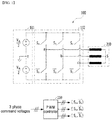
- FIG. 1 is a schematic circuit diagram of a 2-level 3-phase voltage type inverter, which is an example of an inverter used for the energy storage system (ESS), photo-voltaic (PV) inverter, and motor drive technology.
- ESS energy storage system
- PV photo-voltaic
- the inverter 100 may include a direct current (DC) stage 101 and an inverting module 102.
- n of the DC stage 101 represents a virtual DC stage neutral point position.
- the inverting module 102 includes three-phases power switches.
- S a , S b , and S c of the inverting module 102 refer to switching functions of three-phase power switches, respectively.
- An alternating voltage from the inverting module 102 is transferred to a load 200 such as a motor.
- Command voltages of 3 phases may be input to a pulse width modulation (PWM) controller 110.
- PWM controller 110 determines a switching function to be applied to the inverting module 102 and provides the determined switching function to the inverting module 102.
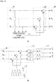
- a triangular carrier wave comparison-based modulation as controlled by the PWM controller 110 will be described with reference to FIG. 2 .
- FIG. 2 shows an example to illustrate a triangular carrier wave comparison-based PWM controlled by a PWM controller in FIG. 1 .
- (a) is an example diagram to illustrate generation of pole voltages
- (b) shows a triangular carrier wave comparison-based PWM.
- An offset command voltage calculation unit 111 calculates an offset command voltage v sn * using three-phase phase command voltages 2A.
- a pole command voltage calculation unit 112 calculates pole command voltages 2B using the three phase command voltages 2A and the offset command voltage v sn * .
- the offset voltage is a component that is common to the three-phase pole voltages. Since the offset voltage means a zero-sequence voltage, the offset voltage does not affect synthesis of an inter-line voltage.
- a period of a triangular carrier wave 2C, which is to be compared with the pole command voltages 2B corresponds to a switching frequency.
- Maximum and minimum values of the carrier wave 2C are V dc 2 and ⁇ V dc 2 respectively.
- a comparison unit 113 compares the pole command voltages 2B with the triangular carrier wave 2C. When, as a result of comparison, a difference between each of the pole command voltages 2B and the triangular carrier wave 2C is positive or zero, the switching function may be output as 1. When, as a result of comparison, a difference between each of the pole command voltages 2B and the triangular carrier wave 2C is negative, the switching function may be output as 0.
- An inversion unit 114 may obtain a switching function of each lower switching element of the inverting module 102. Since each lower switching element operates complementarily with each upper switching element, the switching function may be obtained by inverting an output of the comparison unit 113.
- FIG. 3 shows a diagram of conversion of an output phase voltage according to a switching function into a space vector.
- the output phase voltages are composed of a total of 8 voltages V 0 to V 7 based on the switching functions.
- V 0 and V 7 an voltage is not output.
- the voltage vectors V 0 and V 7 are defined as zero voltage vectors.
- a phase difference between adjacent voltage vectors is 60 degrees.
- Each of voltage vectors V 1 to V 6 has a fixed magnitude of 2 3 V dc .
- voltage vectors V 1 to V 6 are defined as effective voltage vectors.
- the phase command voltages 2A is modulated to an actual voltage via appropriate synthesis between the effective voltage vectors and the zero voltage vectors.
- the offset command voltage calculated by the offset command voltage calculation unit 111 of FIG. 2 may have quite various types.
- V max refers to the largest phase command voltage among the three phase command voltages
- V min refers to the smallest phase command voltage among the three phase command voltages
- the offset command voltage of each of Equation 6 and Equation 7 is based on a continuous pulse width modulation scheme in which the switching functions of all 3 phases change over a single carrier wave period.
- a pulse width modulation scheme in which a switching function of one phase does not change in order to reduce a switching loss is referred to as a discontinuous pulse width modulation scheme.
- a typical discontinuous pulse width modulation scheme is as follows.
- Equation 8 the phase command voltage
- a phase current is defined as Equation 9 below:
- a subscript 'xs' means a specific phase.
- xs becomes as; xs becomes bs for a b-phase; and xs becomes cs for a c-phase.
- ⁇ denotes an AC electric angle.
- ⁇ denotes a phase-difference between the voltage and current.
- V m and I m refer to a peak value of the phase command voltage and the peak value of the current, respectively.
- a typical discontinuous pulse width modulation scheme is 60° discontinuous pulse width modulation scheme (DPWM), in which when a period of a AC frequency is 360 degrees, a switching discontinuous duration from an angular point corresponding to the maximum value of the phase command voltage is 60°.
- An offset command voltage in the 60° discontinuous pulse width modulation scheme may be given by a following Equation 10.
- This DPWM is a pulse width modulation scheme in which the switching loss is minimized when the phase-difference ⁇ between the phase command voltage and phase current is 0°.
- ⁇ v sn * V dc 2 ⁇ v max if , v max + v min ⁇ 0
- v sn * ⁇ V dc 2 ⁇ v min if , v max + v min ⁇ 0
- FIG. 4 shows an operation of an a-phase based 60-degree discontinuous pulse width modulation scheme when a phase command voltage is expressed as a command voltage vector V* in a space vector system.
- This discontinuous pulse width modulation scheme may reduce the switching loss, but may have a disadvantage that the total harmonic distortion (THD) of the current increases.
- the continuous pulse width modulation scheme has a lower current THD than that of the discontinuous pulse width modulation scheme.
- the continuous pulse width modulation scheme has a drawback that the switching loss increases.
- a discontinuous pulse width modulation duration is always fixed to 120°, which is 1/3 of a single period of a fundamental wave.
- an adjustment of the discontinuous modulation duration provides for a degree of freedom for proper selection between the switching loss and current THD. This reduces the switching loss in a region of a low pulse width modulation index compared to the continuous pulse width modulation scheme. Further, a method of reducing the current THD compared to the discontinuous pulse width modulation scheme.
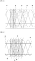
- FIG. 5 is an exemplary diagram for illustrating another implementation of the discontinuous pulse width modulation scheme.
- reference numerals 5A, 5B, and 5C refer to a, b, and c-phases command voltages v as * , v bs * and v cs * respectively.
- a reference numeral 5D represents a peak value of each phase command voltage.
- Each of 5Ds of the 3 phases command voltages is equal to MI V dc 2 when the pulse width modulation index is defined as MI.
- a reference numeral 5E in FIG. 5 represents a magnitude of a voltage at which the discontinuous pulse width modulation begins.
- the magnitude 5E of the voltage at which the discontinuous pulse width modulation begins is defined as MI V dc 2 cos ⁇ 6 .
- the a-phase switching function is always 1.
- the a-phase switching function is always 0. This may be equally applied to the b-phase command voltage 5B and the c-phase command voltage 5C.
- FIG. 6 shows an example to illustrate ADPWM (Adjustable Discontinuous PWM) as another discontinuous pulse width modulation scheme.
- reference numerals 6A, 6B and 6C denote a, b, c-phases command voltages v as * , v bs * and v cs * respectively.
- a reference numeral 6D represents a peak value of each phase command voltage.
- Each of 6Ds of the 3 phases command voltages is equal to MI V dc 2 when the pulse width modulation index is defined as MI.
- a reference numeral 6E in FIG. 6 represents a magnitude of a voltage at which the discontinuous pulse width modulation begins. The magnitude 6E of the voltage at which the discontinuous pulse width modulation begins is defined as MI V dc 2 cos ⁇ D .
- ⁇ D refers to a discontinuous pulse width modulation angle representing a length of a discontinuous pulse width modulation duration.
- ⁇ D is zero, the space vector pulse width modulation as a continuous pulse width modulation scheme is achieved.
- ⁇ D is 30°, the 60° discontinuous pulse width modulation scheme as described above is achieved.
- a reference numeral 6F means a duration during which a corresponding phase switching element does not perform a switching operation.
- a reference numeral 6G means a duration during which a corresponding phase switching element performs a normal switching operation.
- the a-phase switching function is always 0, so that the a-phase switching element performs a switching operation for the duration 6F for which the a-phase switching element does not perform the switching operation. This may be equally applied to the b-phase command voltage 6B and the c-phase command voltage 6C.
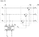
- FIG. 7 shows a configuration diagram of an implementation of the ADPWM.
- an offset command voltage calculation unit 711 receives 3 phases command voltages 7A, a DC stage voltage V dc and a k value defined in the above Equation 13 and then calculates an offset command voltage.
- a pole command voltage calculation unit 712 adds the offset command voltage V* sn to the phase command voltages 7A to calculate three-phases pole command voltages 7B.
- the discontinuous pulse width modulation scheme as described above may reduce the switching loss
- the discontinuous pulse width modulation scheme has the disadvantage of increasing the THD of the current.
- the user may appropriately control a trade-off between the switching loss and the current THD by adjusting the discontinuous modulation duration.
- the discontinuous pulse width modulation scheme may be used to reduce the switching loss.
- the current THD when using the discontinuous pulse width modulation scheme, the current THD must deteriorate.
- a conventional method may reduce the switching loss in a region of a low modulation index MI as compared to the continuous voltage modulation scheme. Using the conventional method, the current THD may be reduced compared to the discontinuous voltage modulation scheme.
- the conventional method as described above has a problem of having a minimum loss only in a state where the power factor is 1 in which the phase difference between the voltage and the current is 0°.
- the user may appropriately control the trade-off between the switching loss and the current THD by adjusting the discontinuous modulation duration.
- an inverter-controlling device may always achieve a minimum loss for a certain discontinuous modulation duration regardless of the power factor.
- the inverter-controlling device in accordance with the present disclosure is applied to a two-level three-phases voltage type inverter used for the energy storage system (ESS), photo-voltaic (PV) inverter, and motor drive technology, as shown in FIG. 1 .
- the inverter-controlling device in accordance with the present disclosure is based on a triangular wave pulse width modulation scheme using an offset voltage.
- FIG. 2 the configuration of FIG. 2 in which the pole command voltages and the triangular carrier wave are compared to each other is applied equally to the present disclosure.
- both switching discontinuous angular durations are present around an angular point corresponding to a maximum value of each phase command voltage.
- Each of both switching discontinuous angular durations is ⁇ D .
- the switching loss is minimized when the phase-difference ⁇ between each phase command voltage and each phase current is zero. That is, both switching discontinuous angular durations occurs around an angular point corresponding to a maximum value of each phase current.
- Each of both switching discontinuous angular durations is ⁇ D . Therefore, this scheme has a minimum loss compared to other discontinuous pulse width modulation schemes.
- a minimal loss may be achieved using a virtual command voltage in spite of a non-zero phase-difference between the actual command voltage and actual output current. That is, regardless of the power factor, the minimum loss may occur at a certain discontinuous modulation angle ⁇ D .
- One embodiment of the present disclosure may be implemented by applying the ADPWM based on the virtual command voltage such that a phase of the virtual command voltage coincides with a phase of the current as much as possible.
- FIG. 8 shows an example configuration of converting the phase command voltage to the pole command voltage in the inverter-controlling device in accordance with an embodiment of the present disclosure.
- an inverter-controlling device in accordance with an embodiment of the present disclosure may include an offset command voltage calculation unit 10 and a pole command voltage calculation unit 20.
- the inverter-controlling device in accordance with an embodiment of the present disclosure calculates an offset command voltage with a minimal loss for the ADPWM.
- the offset command voltage calculation unit 10 uses phase voltages 8A of three phases, a DC stage voltage V DC , the k value, a phase-difference ⁇ between each phase command voltage and each phase inverter output current to calculate each phase offset command voltage.
- the k value is defined as MIcos ⁇ D
- the pulse width modulation index is denoted as MI
- ⁇ D refers to the discontinuous modulation angle which may control the discontinuous modulation duration.
- the pole command voltage calculation unit 20 may generate each pole command voltage 8B by adding each offset command voltage to each phase command voltage 8A.
- FIG. 9 shows a detailed configuration of the offset command voltage calculation unit 10 in FIG. 8 .
- the offset command voltage calculation unit 10 in accordance with an embodiment of the present disclosure includes a first coordinate transform unit 11, a rotation transform unit 12, an angular transform unit 13, a second coordinate transform unit 14, and an offset command voltage generation unit 15.
- the first coordinate transform unit 11 may transform a, b, and c-phase variables into stationary reference frame d and q axis variables and may be expressed as Equation 14 below. 2 3 1 ⁇ 1 2 ⁇ 1 2 0 3 2 ⁇ 3 2
- the 3-phase phase command voltages may be transformed by the first coordinate transform unit 11 into the d and q-axis command voltages as expressed in Equation 15 below:
- v ds * v qs * 2 3 1 ⁇ 1 2 ⁇ 1 2 0 3 2 ⁇ 3 2 v as * v bs * v cs *
- the command voltages based the d and q axes passing through the first coordinate transform unit 11 may be transformed, by the rotation transform unit 12, into rotated d and q axis command voltages as expressed as Equation 17 below:
- v ds V v qs V cos ⁇ V ⁇ sin ⁇ V sin ⁇ V cos ⁇ V v ds * v qs *
- the second coordinate transform unit 14 may coordinate-transform the d and q axis variables to a, b, and c-phase variables, and may be expressed as Equation 18 below: 1 0 ⁇ 1 2 3 2 ⁇ 1 2 ⁇ 3 2
- the angular transform unit 13 may receive the phase-difference ⁇ between the command voltage and the output current to generate the angular information used for the rotation transformation. This will be described in more detail later.
- the offset command voltage generation unit 15 may generate the offset command voltages using the three phases command voltages 8A, the DC stage voltage, the k value, and the virtual three phases command voltages.
- FIG. 10 is a detailed block diagram of an embodiment of the offset command voltage generation unit 15 of FIG. 9 .
- the offset command voltage generation unit 15 in accordance with one embodiment of the present disclosure may include a first determination unit 31, a second determination unit 32, and a third determination unit 33.
- the generation of the offset command voltage in accordance with an embodiment of the present disclosure may use the three-phase command voltages.
- FIG. 11 is an example diagram for illustrating a relation between a phase difference ⁇ between a command voltage and an output current and a virtual phase-difference ⁇ V as an angular information used for generation of a virtual phase command voltage according to one embodiment of the present disclosure.
- (a) indicates a command voltage space vector V * , a virtual command voltage space vector V V , and a current space vector i when a phase-difference ⁇ between the command voltage and the output current is 0 ⁇ ⁇ ⁇ ⁇ 3 ⁇ ⁇ D .
- both ⁇ D sized discontinuous modulation durations are present around a current vector i
- the phase difference between the current vector and the virtual command voltage vector is 0.
- (b) indicates a command voltage space vector V *, a virtual command voltage space vector V V , and a current space vector i when a phase-difference ⁇ between the command voltage and the output current is ⁇ 3 ⁇ ⁇ D ⁇ ⁇ ⁇ ⁇ 2 ⁇ ⁇ D .
- a sector 1, sector 6, sector 3, and sector 4 only correspond to the discontinuous pulse width modulation duration. Therefore, this may disallow the coincidence between the phases of the virtual vector and the current vector.
- phase-difference ⁇ between the phases of the command voltage and the output current is ⁇ 3 ⁇ ⁇ D ⁇ ⁇ ⁇ ⁇ 2 ⁇ ⁇ D
- ⁇ V ⁇ 3 ⁇ ⁇ D .
- (c) indicates a command voltage space vector V *, a virtual command voltage space vector V V , and a current space vector i when a phase-difference ⁇ between the command voltage and the output current is ⁇ 2 ⁇ ⁇ D ⁇ ⁇ ⁇ ⁇ 2 .
- a sector 1, sector 6, sector 3, and sector 4 only correspond to the discontinuous pulse width modulation duration. Therefore, this may disallow the coincidence between the phases of the virtual vector and the current vector.
- a difference between the phase of the virtual voltage vector and the phase of the current vector should be minimized.
- the phase-difference between the virtual command voltage vector V V and the current vector is fixed to ⁇ 6 . In this way, the switching loss can be minimized by locating the discontinuous pulse width modulation duration appropriately into the sector 1, sector 6, sector 3, and sector 4 based on the current vector.
- phase-difference ⁇ between the command voltage and the output current is ⁇ 2 ⁇ ⁇ D ⁇ ⁇ ⁇ ⁇ 2
- ⁇ V ⁇ ⁇ ⁇ 6 .
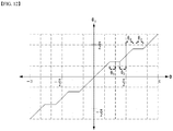
- FIG. 12 is an example diagram to illustrate the operation of the angular transform unit 13 of FIG. 9 .
- FIG. 12 shows a relationship between the phase-difference ⁇ between the command voltage and the output current and the virtual phase-difference ⁇ V used for the generation of the virtual command voltage.
- FIG. 13 is an example graph for illustrating the switching loss in the inverter-controlling device in accordance with one embodiment of the present disclosure.
- a horizontal axis in FIG. 13 denotes the phase-difference between the command voltage and the output current.
- a vertical axis represents the ratio of the switching loss of the discontinuous pulse width modulation scheme to the switching loss of the continuous pulse width modulation scheme. That is, when the switching loss ratio is 1, the same switching loss between the continuous and discontinuous pulse width modulation schemes is exhibited.
- the ratio 0.5 means that the switching loss of the discontinuous pulse width modulation scheme is reduced by 50% compared with the continuous pulse width modulation scheme.
- reference numerals 13A and 13B indicate the switching loss ratio according to the conventional ADPWM and the switching loss ratio according to one embodiment of the present disclosure respectively when a discontinuous modulation angle ⁇ D thereof is set to 6°.
- Reference numerals 14A and 14B indicate the switching loss ratio according to the conventional ADPWM and the switching loss ratio according to one embodiment of the present disclosure respectively when a discontinuous modulation angle ⁇ D thereof is set to 12°.
- Reference numerals 15A and 15B indicate the switching loss ratio according to the conventional ADPWM and the switching loss ratio according to one embodiment of the present disclosure respectively when a discontinuous modulation angle ⁇ D thereof is set to 18°.
- Reference numerals 16A and 16B indicate the switching loss ratio according to the conventional ADPWM and the switching loss ratio according to one embodiment of the present disclosure respectively when a discontinuous modulation angle ⁇ D thereof is set to 24°.
- Reference numerals 17A and 17B indicate the switching loss ratio according to the conventional ADPWM and the switching loss ratio according to one embodiment of the present disclosure respectively when a discontinuous modulation angle ⁇ D thereof is set to 30°.
- the conventional ADPWM exhibits a minimum loss when the phase difference ⁇ between the command voltage and the output current is zero at a given discontinuous pulse width modulation angle.
- the control device in accordance with the present disclosure exhibits a possible minimum loss at a given discontinuous pulse width modulation angle regardless of the phase-difference ⁇ .
- control device in accordance with the present disclosure uses the phase-difference between the command voltage and output current, and the discontinuous modulation angles that are used to control the discontinuous pulse width modulation duration. Further, the control device in accordance with the present disclosure may use the generated virtual command voltage, thereby to always exhibit the possible minimum loss at a given discontinuous pulse width modulation duration regardless of the power factor.
- the virtual phase command voltage may be generated via the rotational transformation of the actual phase command voltage.
- the rotation angle used for this rotation transformation may be determined using the phase-difference between the command voltage and the output current and the discontinuous modulation angle.
- the pulse width modulation may be performed using the virtual phase command voltage, the actual phase command voltage and the discontinuous modulation angle.
- the discontinuous modulation duration may be adjusted to properly control the trade-off between the switching loss and current THD.
- the present scheme always result in a minimum loss in a given discontinuous modulation duration regardless of the power factor.
Landscapes
- Engineering & Computer Science (AREA)
- Power Engineering (AREA)
- Inverter Devices (AREA)
Applications Claiming Priority (1)
| Application Number | Priority Date | Filing Date | Title |
|---|---|---|---|
| KR1020180062310A KR102109574B1 (ko) | 2018-05-31 | 2018-05-31 | 인버터 제어장치 |
Publications (1)
| Publication Number | Publication Date |
|---|---|
| EP3576286A1 true EP3576286A1 (de) | 2019-12-04 |
Family
ID=65724326
Family Applications (1)
| Application Number | Title | Priority Date | Filing Date |
|---|---|---|---|
| EP19161447.8A Withdrawn EP3576286A1 (de) | 2018-05-31 | 2019-03-07 | Vorrichtung zur steuerung eines wechselrichters |
Country Status (5)
| Country | Link |
|---|---|
| US (1) | US10498216B1 (de) |
| EP (1) | EP3576286A1 (de) |
| JP (1) | JP6695598B2 (de) |
| KR (1) | KR102109574B1 (de) |
| CN (1) | CN110557039B (de) |
Cited By (2)
| Publication number | Priority date | Publication date | Assignee | Title |
|---|---|---|---|---|
| CN115441764A (zh) * | 2021-06-04 | 2022-12-06 | 罗克韦尔自动化技术公司 | 减少逆变器的多相输出电压的调制中的延迟的系统和方法 |
| KR20240161394A (ko) * | 2023-05-04 | 2024-11-12 | 중앙대학교 산학협력단 | 하이브리드 오프셋 전압을 이용한 삼상 전압원 인버터의 제어 방법 |
Families Citing this family (10)
| Publication number | Priority date | Publication date | Assignee | Title |
|---|---|---|---|---|
| KR102599386B1 (ko) * | 2018-07-11 | 2023-11-09 | 현대자동차주식회사 | 모터 구동을 위한 인버터 제어 장치 및 방법 |
| KR102483999B1 (ko) * | 2020-11-27 | 2022-12-30 | 연세대학교 산학협력단 | 3 상 인버터의 제어 방법 및 3 상 인버터의 제어 장치 |
| CN115473463B (zh) * | 2021-06-10 | 2025-08-01 | 香港城市大学深圳研究院 | 开绕组三相永磁同步电机模型预测控制方法及驱动器 |
| CN114421837B (zh) * | 2021-08-31 | 2023-12-22 | 宁波诺丁汉大学 | 一种功率因数自适应的不连续脉宽调制算法 |
| CN116054620A (zh) * | 2021-10-28 | 2023-05-02 | 台达电子工业股份有限公司 | 功率转换器的控制方法与功率转换器 |
| CN114244229B (zh) * | 2021-12-22 | 2024-02-27 | 北京国家新能源汽车技术创新中心有限公司 | 一种电机控制方法、电机、车辆、储存介质以及计算机 |
| EP4210210A1 (de) | 2022-01-08 | 2023-07-12 | Goodrich Aerospace Services Private Limited | Systeme und verfahren für raumvektorpulsbreitemodulationstechnik |
| KR102621858B1 (ko) * | 2022-01-28 | 2024-01-05 | 엘지전자 주식회사 | 모터 제어 장치, 의류처리장치의 제어 장치, 모터 제어 장치의 모터 제어 방법 및 의류처리장치의 제어 장치의 모터 제어 방법 |
| CN115021604B (zh) * | 2022-06-21 | 2026-01-23 | 珠海格力电器股份有限公司 | 光伏并网逆变器的调制方法、装置、逆变器及存储介质 |
| US12549113B2 (en) * | 2023-01-31 | 2026-02-10 | Cummins Power Generation Inc. | Rebalancing pulse width modulation signals for power systems |
Citations (3)
| Publication number | Priority date | Publication date | Assignee | Title |
|---|---|---|---|---|
| US20120249046A1 (en) * | 2011-03-30 | 2012-10-04 | Bose Corporation | Rate Limited Common Mode Control for Pulse-Width Modulation Drives |
| EP3082247A2 (de) * | 2015-04-14 | 2016-10-19 | LSIS Co., Ltd. | Offsetspannungsgenerator und verfahren zur erzeugung von offsetspannung eines drehstromwechselrichters |
| US9654028B1 (en) * | 2016-03-24 | 2017-05-16 | Eaton Corporation | System and method for maximizing efficiency of three-phase inverter-based power systems |
Family Cites Families (8)
| Publication number | Priority date | Publication date | Assignee | Title |
|---|---|---|---|---|
| US6023417A (en) * | 1998-02-20 | 2000-02-08 | Allen-Bradley Company, Llc | Generalized discontinuous pulse width modulator |
| US7592765B2 (en) * | 2006-10-25 | 2009-09-22 | Gm Global Technology Operations, Inc. | Method and system for controlling synchronous motor drive systems |
| JP5194998B2 (ja) * | 2008-04-30 | 2013-05-08 | ダイキン工業株式会社 | インバータ装置及びそれを搭載した空気調和装置 |
| US8441820B2 (en) * | 2010-09-29 | 2013-05-14 | General Electric Company | DC-link voltage balancing system and method for multilevel converters |
| US9369071B2 (en) * | 2014-02-20 | 2016-06-14 | Ford Global Technologies, Llc | Discontinuous pulse width modulation |
| KR102028328B1 (ko) * | 2015-04-14 | 2019-10-04 | 엘에스산전 주식회사 | 계통 연계형 인버터 제어장치 |
| KR102009509B1 (ko) * | 2015-04-14 | 2019-08-13 | 엘에스산전 주식회사 | 3상 인버터의 옵셋 전압 생성 장치 및 방법 |
| KR101721238B1 (ko) * | 2015-07-01 | 2017-03-29 | 아주대학교 산학협력단 | 불연속 전압 변조 방식 기반의 계통 연계형 전력 변환 장치 및 방법 |
-
2018
- 2018-05-31 KR KR1020180062310A patent/KR102109574B1/ko active Active
-
2019
- 2019-02-25 JP JP2019031975A patent/JP6695598B2/ja active Active
- 2019-03-07 US US16/295,844 patent/US10498216B1/en active Active
- 2019-03-07 EP EP19161447.8A patent/EP3576286A1/de not_active Withdrawn
- 2019-03-12 CN CN201910183762.2A patent/CN110557039B/zh active Active
Patent Citations (3)
| Publication number | Priority date | Publication date | Assignee | Title |
|---|---|---|---|---|
| US20120249046A1 (en) * | 2011-03-30 | 2012-10-04 | Bose Corporation | Rate Limited Common Mode Control for Pulse-Width Modulation Drives |
| EP3082247A2 (de) * | 2015-04-14 | 2016-10-19 | LSIS Co., Ltd. | Offsetspannungsgenerator und verfahren zur erzeugung von offsetspannung eines drehstromwechselrichters |
| US9654028B1 (en) * | 2016-03-24 | 2017-05-16 | Eaton Corporation | System and method for maximizing efficiency of three-phase inverter-based power systems |
Non-Patent Citations (3)
| Title |
|---|
| BIERHOFF M ET AL: "An Analysis on Switching Loss Optimized PWM Strategies for Three Phase PWM Voltage Source Converters", PROCEEDINGS OF THE INTERNATIONAL CONFERENCE ON INDUSTRIAL ELECTRONICS CONTROL AND INSTRUMENTATION, IEEE, TAIPEI, TAIWAN, 5 November 2007 (2007-11-05), pages 1512 - 1517, XP031234988, ISBN: 978-1-4244-0783-5 * |
| LEE HAK-JUN ET AL: "A carrier-based adjustable discontinuous PWM for three-phase voltage source inverter", 2015 IEEE ENERGY CONVERSION CONGRESS AND EXPOSITION (ECCE), IEEE, 20 September 2015 (2015-09-20), pages 2870 - 2875, XP032800951, DOI: 10.1109/ECCE.2015.7310062 * |
| OHTA YOSHITO ET AL: "Controller design of a grid-tie inverter bypassing DQ transformation", 52ND IEEE CONFERENCE ON DECISION AND CONTROL, IEEE, 10 December 2013 (2013-12-10), pages 2927 - 2932, XP032577063, ISSN: 0743-1546, ISBN: 978-1-4673-5714-2, [retrieved on 20140307], DOI: 10.1109/CDC.2013.6760328 * |
Cited By (4)
| Publication number | Priority date | Publication date | Assignee | Title |
|---|---|---|---|---|
| CN115441764A (zh) * | 2021-06-04 | 2022-12-06 | 罗克韦尔自动化技术公司 | 减少逆变器的多相输出电压的调制中的延迟的系统和方法 |
| EP4099558A1 (de) * | 2021-06-04 | 2022-12-07 | Rockwell Automation Technologies, Inc. | System und verfahren zur reduzierung der verzögerung bei der modulation einer mehrphasigen ausgangsspannung eines wechselrichters |
| US11539283B1 (en) | 2021-06-04 | 2022-12-27 | Rockwell Automation Technologies, Inc. | System and method for reducing delay in the modulation of a multi-phase output voltage from an inverter |
| KR20240161394A (ko) * | 2023-05-04 | 2024-11-12 | 중앙대학교 산학협력단 | 하이브리드 오프셋 전압을 이용한 삼상 전압원 인버터의 제어 방법 |
Also Published As
| Publication number | Publication date |
|---|---|
| JP2019213442A (ja) | 2019-12-12 |
| US10498216B1 (en) | 2019-12-03 |
| JP6695598B2 (ja) | 2020-05-20 |
| CN110557039B (zh) | 2021-11-02 |
| KR102109574B1 (ko) | 2020-05-12 |
| CN110557039A (zh) | 2019-12-10 |
| US20190372453A1 (en) | 2019-12-05 |
| KR20190136501A (ko) | 2019-12-10 |
Similar Documents
| Publication | Publication Date | Title |
|---|---|---|
| EP3576286A1 (de) | Vorrichtung zur steuerung eines wechselrichters | |
| CN104242775B (zh) | 双逆变器供电的开放式绕组永磁同步电机系统零序电流抑制方法 | |
| US10153714B2 (en) | Adaptive pulse width modulation in motor control systems | |
| Chun et al. | Development of adaptive hysteresis band current control strategy of PWM inverter with constant switching frequency | |
| KR20160122923A (ko) | 3상 인버터의 옵셋 전압 생성 장치 및 방법 | |
| WO2004062078A1 (ja) | 空気調和装置用モータ駆動装置 | |
| KR20160122922A (ko) | 3상 인버터의 옵셋 전압 생성 장치 및 방법 | |
| EP3522358A1 (de) | Umrichtersteuerungsvorrichtung | |
| JP2023025679A (ja) | モーター駆動装置 | |
| JP2020137233A (ja) | 電力変換装置、発電電動機の制御装置、および、電動パワーステアリング装置 | |
| Lipo | Switching angles and DC link voltages optimization for multilevel cascade inverters | |
| Zhong et al. | Reference voltage self-equalization-based modulation strategy for open-end winding PMSM fed by dual three-level inverters with common DC bus | |
| US11303224B2 (en) | Inverter device with high follow-up capability | |
| Ren et al. | A non-nearest space vector modulation with reduced common-mode voltage for three-level ANPC inverter fed PMSM drives | |
| CN116345858A (zh) | 一种应用于中点钳位三电平逆变器的中点电位控制方法 | |
| JP7609705B2 (ja) | 電力変換装置 | |
| Kim et al. | A comparison of dpwm and inverter loss energy based fcs-mpc for ipmsm | |
| Jang et al. | Indirect matrix converter for permanent-magnet-synchronous-motor drives by improved torque predictive control | |
| Lim et al. | Two-phase commutation control method of open-end winding PMSM with reduced loss for low torque operation | |
| Ohata et al. | Zero-sequence current control dual-inverter with common source during the single-side 6-step operation | |
| Kondratenko et al. | Increasing the utilization of DC-link voltage of a five-leg VSI based on rotor angle control of dual induction motors | |
| Saeidabadi et al. | Simplified model predictive control for a five-phase PMSM using four-leg inverter | |
| JP4277360B2 (ja) | 3レベルインバータの制御装置 | |
| Kumar Modi et al. | Analysis and comparison of overmodulation algorithms for space vector modulated voltage source inverter | |
| Surana et al. | Synthesis of a Modulating Waveform for a Carrier-Based Dodecagonal Space Vector PWM Signal Generation for a Split-Phase Induction Motor Drive |
Legal Events
| Date | Code | Title | Description |
|---|---|---|---|
| PUAI | Public reference made under article 153(3) epc to a published international application that has entered the european phase |
Free format text: ORIGINAL CODE: 0009012 |
|
| STAA | Information on the status of an ep patent application or granted ep patent |
Free format text: STATUS: THE APPLICATION HAS BEEN PUBLISHED |
|
| AK | Designated contracting states |
Kind code of ref document: A1 Designated state(s): AL AT BE BG CH CY CZ DE DK EE ES FI FR GB GR HR HU IE IS IT LI LT LU LV MC MK MT NL NO PL PT RO RS SE SI SK SM TR |
|
| AX | Request for extension of the european patent |
Extension state: BA ME |
|
| STAA | Information on the status of an ep patent application or granted ep patent |
Free format text: STATUS: REQUEST FOR EXAMINATION WAS MADE |
|
| 17P | Request for examination filed |
Effective date: 20200604 |
|
| RBV | Designated contracting states (corrected) |
Designated state(s): AL AT BE BG CH CY CZ DE DK EE ES FI FR GB GR HR HU IE IS IT LI LT LU LV MC MK MT NL NO PL PT RO RS SE SI SK SM TR |
|
| STAA | Information on the status of an ep patent application or granted ep patent |
Free format text: STATUS: EXAMINATION IS IN PROGRESS |
|
| 17Q | First examination report despatched |
Effective date: 20210223 |
|
| STAA | Information on the status of an ep patent application or granted ep patent |
Free format text: STATUS: THE APPLICATION HAS BEEN WITHDRAWN |
|
| 18W | Application withdrawn |
Effective date: 20240307 |