EP3570018A1 - Gasdetektor und gasdetektionsverfahren - Google Patents
Gasdetektor und gasdetektionsverfahren Download PDFInfo
- Publication number
- EP3570018A1 EP3570018A1 EP17890993.3A EP17890993A EP3570018A1 EP 3570018 A1 EP3570018 A1 EP 3570018A1 EP 17890993 A EP17890993 A EP 17890993A EP 3570018 A1 EP3570018 A1 EP 3570018A1
- Authority
- EP
- European Patent Office
- Prior art keywords
- metal oxide
- oxide semiconductor
- sensor
- mobile electronic
- electronic device
- Prior art date
- Legal status (The legal status is an assumption and is not a legal conclusion. Google has not performed a legal analysis and makes no representation as to the accuracy of the status listed.)
- Granted
Links
- 238000001514 detection method Methods 0.000 title claims description 14
- 239000007789 gas Substances 0.000 claims abstract description 140
- 229910044991 metal oxide Inorganic materials 0.000 claims abstract description 54
- 150000004706 metal oxides Chemical class 0.000 claims abstract description 54
- 239000004065 semiconductor Substances 0.000 claims abstract description 54
- 238000010438 heat treatment Methods 0.000 claims abstract description 28
- 238000004140 cleaning Methods 0.000 claims description 22
- 238000005070 sampling Methods 0.000 claims description 4
- 238000000034 method Methods 0.000 claims description 3
- 231100000572 poisoning Toxicity 0.000 abstract description 2
- 230000000607 poisoning effect Effects 0.000 abstract description 2
- -1 siloxanes Chemical class 0.000 abstract description 2
- 239000010408 film Substances 0.000 description 15
- 238000011109 contamination Methods 0.000 description 13
- 229920001296 polysiloxane Polymers 0.000 description 13
- 238000010586 diagram Methods 0.000 description 12
- LFQSCWFLJHTTHZ-UHFFFAOYSA-N Ethanol Chemical compound CCO LFQSCWFLJHTTHZ-UHFFFAOYSA-N 0.000 description 8
- 239000000356 contaminant Substances 0.000 description 8
- KPUWHANPEXNPJT-UHFFFAOYSA-N disiloxane Chemical class [SiH3]O[SiH3] KPUWHANPEXNPJT-UHFFFAOYSA-N 0.000 description 7
- 239000000758 substrate Substances 0.000 description 5
- XOLBLPGZBRYERU-UHFFFAOYSA-N tin dioxide Chemical compound O=[Sn]=O XOLBLPGZBRYERU-UHFFFAOYSA-N 0.000 description 4
- 230000001133 acceleration Effects 0.000 description 3
- 238000012986 modification Methods 0.000 description 3
- 230000004048 modification Effects 0.000 description 3
- 239000003960 organic solvent Substances 0.000 description 3
- 238000006116 polymerization reaction Methods 0.000 description 3
- 238000004891 communication Methods 0.000 description 2
- 150000001875 compounds Chemical class 0.000 description 2
- VNWKTOKETHGBQD-UHFFFAOYSA-N methane Chemical compound C VNWKTOKETHGBQD-UHFFFAOYSA-N 0.000 description 2
- 238000009423 ventilation Methods 0.000 description 2
- 230000003197 catalytic effect Effects 0.000 description 1
- 239000002537 cosmetic Substances 0.000 description 1
- 230000007423 decrease Effects 0.000 description 1
- 230000003247 decreasing effect Effects 0.000 description 1
- 230000001419 dependent effect Effects 0.000 description 1
- PJXISJQVUVHSOJ-UHFFFAOYSA-N indium(III) oxide Inorganic materials [O-2].[O-2].[O-2].[In+3].[In+3] PJXISJQVUVHSOJ-UHFFFAOYSA-N 0.000 description 1
- 230000005389 magnetism Effects 0.000 description 1
- 239000000463 material Substances 0.000 description 1
- 238000005459 micromachining Methods 0.000 description 1
- 230000002265 prevention Effects 0.000 description 1
- 229910052710 silicon Inorganic materials 0.000 description 1
- 239000010703 silicon Substances 0.000 description 1
- 229920002379 silicone rubber Polymers 0.000 description 1
- 238000001179 sorption measurement Methods 0.000 description 1
- 239000010409 thin film Substances 0.000 description 1
Images


Classifications
-
- G—PHYSICS
- G01—MEASURING; TESTING
- G01N—INVESTIGATING OR ANALYSING MATERIALS BY DETERMINING THEIR CHEMICAL OR PHYSICAL PROPERTIES
- G01N27/00—Investigating or analysing materials by the use of electric, electrochemical, or magnetic means
- G01N27/02—Investigating or analysing materials by the use of electric, electrochemical, or magnetic means by investigating impedance
- G01N27/04—Investigating or analysing materials by the use of electric, electrochemical, or magnetic means by investigating impedance by investigating resistance
- G01N27/12—Investigating or analysing materials by the use of electric, electrochemical, or magnetic means by investigating impedance by investigating resistance of a solid body in dependence upon absorption of a fluid; of a solid body in dependence upon reaction with a fluid, for detecting components in the fluid
- G01N27/122—Circuits particularly adapted therefor, e.g. linearising circuits
- G01N27/123—Circuits particularly adapted therefor, e.g. linearising circuits for controlling the temperature
- G01N27/124—Circuits particularly adapted therefor, e.g. linearising circuits for controlling the temperature varying the temperature, e.g. in a cyclic manner
-
- B—PERFORMING OPERATIONS; TRANSPORTING
- B81—MICROSTRUCTURAL TECHNOLOGY
- B81B—MICROSTRUCTURAL DEVICES OR SYSTEMS, e.g. MICROMECHANICAL DEVICES
- B81B7/00—Microstructural systems; Auxiliary parts of microstructural devices or systems
- B81B7/0083—Temperature control
- B81B7/0087—On-device systems and sensors for controlling, regulating or monitoring
-
- B—PERFORMING OPERATIONS; TRANSPORTING
- B81—MICROSTRUCTURAL TECHNOLOGY
- B81B—MICROSTRUCTURAL DEVICES OR SYSTEMS, e.g. MICROMECHANICAL DEVICES
- B81B7/00—Microstructural systems; Auxiliary parts of microstructural devices or systems
- B81B7/0083—Temperature control
- B81B7/009—Maintaining a constant temperature by heating or cooling
- B81B7/0096—Maintaining a constant temperature by heating or cooling by heating
-
- G—PHYSICS
- G01—MEASURING; TESTING
- G01N—INVESTIGATING OR ANALYSING MATERIALS BY DETERMINING THEIR CHEMICAL OR PHYSICAL PROPERTIES
- G01N27/00—Investigating or analysing materials by the use of electric, electrochemical, or magnetic means
- G01N27/02—Investigating or analysing materials by the use of electric, electrochemical, or magnetic means by investigating impedance
- G01N27/04—Investigating or analysing materials by the use of electric, electrochemical, or magnetic means by investigating impedance by investigating resistance
- G01N27/12—Investigating or analysing materials by the use of electric, electrochemical, or magnetic means by investigating impedance by investigating resistance of a solid body in dependence upon absorption of a fluid; of a solid body in dependence upon reaction with a fluid, for detecting components in the fluid
- G01N27/128—Microapparatus
-
- G—PHYSICS
- G01—MEASURING; TESTING
- G01N—INVESTIGATING OR ANALYSING MATERIALS BY DETERMINING THEIR CHEMICAL OR PHYSICAL PROPERTIES
- G01N27/00—Investigating or analysing materials by the use of electric, electrochemical, or magnetic means
- G01N27/02—Investigating or analysing materials by the use of electric, electrochemical, or magnetic means by investigating impedance
- G01N27/04—Investigating or analysing materials by the use of electric, electrochemical, or magnetic means by investigating impedance by investigating resistance
- G01N27/14—Investigating or analysing materials by the use of electric, electrochemical, or magnetic means by investigating impedance by investigating resistance of an electrically-heated body in dependence upon change of temperature
- G01N27/18—Investigating or analysing materials by the use of electric, electrochemical, or magnetic means by investigating impedance by investigating resistance of an electrically-heated body in dependence upon change of temperature caused by changes in the thermal conductivity of a surrounding material to be tested
-
- G—PHYSICS
- G01—MEASURING; TESTING
- G01N—INVESTIGATING OR ANALYSING MATERIALS BY DETERMINING THEIR CHEMICAL OR PHYSICAL PROPERTIES
- G01N27/00—Investigating or analysing materials by the use of electric, electrochemical, or magnetic means
- G01N27/26—Investigating or analysing materials by the use of electric, electrochemical, or magnetic means by investigating electrochemical variables; by using electrolysis or electrophoresis
- G01N27/416—Systems
-
- G—PHYSICS
- G01—MEASURING; TESTING
- G01N—INVESTIGATING OR ANALYSING MATERIALS BY DETERMINING THEIR CHEMICAL OR PHYSICAL PROPERTIES
- G01N33/00—Investigating or analysing materials by specific methods not covered by groups G01N1/00 - G01N31/00
- G01N33/0004—Gaseous mixtures, e.g. polluted air
- G01N33/0009—General constructional details of gas analysers, e.g. portable test equipment
- G01N33/0011—Sample conditioning
- G01N33/0013—Sample conditioning by a chemical reaction
Definitions
- the present invention relates to a gas detector and a gas detection method.
- Patent Document 1 JP5748211B .
- a MEMS gas sensor is operated with a 30 seconds period and is heated to 100°C for 0.4 second in order to remove contaminants such as ethanol and siloxanes. Then, the gas sensor is heated about 500°C for detecting methane.
- Patent Document 1 JP5748211B
- gas sensors When gas sensors are installed within mobile electronic devices such as smartphones, gas sensors are sometimes confined in brief cases, handbags, drawers, and so on. They are closed spaces and have poor ventilation. Further, siloxane gases are generated from silicone rubbers used in the covers of the mobile electronic devices; they are also generated from silicone compounds contained in cosmetics within the handbags or drawers, and form other small items. MEMS gas sensors are contaminated by the siloxane gases in these closed spaces, and as a result, the response of the gas sensors to gases decreases in both the magnitude and the speed.
- the object of the invention is to prevent the contamination of MEMS gas sensors installed within mobile electronic devices.
- the gas detector according to the invention comprises a MEMS gas sensor having a film-like metal oxide semiconductor having an electrical resistance varying according to gases and a heater; and a drive circuit supplying electric power to the heater intermittently to heat the metal oxide semiconductor to an operating temperature and sampling the electrical resistance of the metal oxide semiconductor at the operating temperature.
- the gas detector is configured to be installed within a mobile electronic device.
- the drive circuit halts the heating of the metal oxide semiconductor to the operating temperature when a sensor of the mobile electronic device detects the mobile electronic device is placed in a closed space and then resumes the heating of the metal oxide semiconductor to the operating temperature when the sensor of the mobile electronic device detects the mobile electronic device has been taken out from the closed space.
- the gas detection method uses a MEMS gas sensor having a film-like metal oxide semiconductor having an electrical resistance varying according to gases, and a heater, and supplies electric power to the heater intermittently to heat the metal oxide semiconductor to an operating temperature by a drive circuit, and samples the electrical resistance of the metal oxide semiconductor at the operating temperature by the drive circuit. Further, the gas detector is installed within a mobile electronic device.
- the gas detection method according to the invention comprises:
- the operation of MEMS gas sensors is halted; in other words, the heating of the metal oxide semiconductor of the gas sensors to the operating temperature is halted. Then, the contamination of the MEMS gas sensors is prevented.
- the mobile electronic devices are contained in closed spaces where ventilation is insufficient, the contaminant gas concentrations increase, and therefore, the contamination arises.
- the fact that the mobile electronic devices are in closed spaces is detectable by sensors in the mobile electronic devices.
- MEMS gas sensors are more easily contaminated than conventional gas sensors, since the heating periods of MEMS gas sensors are made shorter for reducing their power consumptions.
- the senor of the mobile electronic device is an ambient light sensor or a proximity sensor. These sensors are installed in many of the mobile electronic devices.
- the ambient light sensor may detect that the surroundings are dark and therefore that the device is placed in a closed space.
- the proximity sensor may detect that the inner sides of briefcases, handbags, drawers, or the like and therefore that the device is placed in a closed space.
- the drive circuit is configured and programmed to heat the metal oxide semiconductor to the operating temperature with a predetermined period and to halt the heating of the metal oxide semiconductor to the operating temperature when the sensor of the mobile electronic device detects the mobile electronic device is placed in a closed space over a plurality of the periods.
- the contamination is caused when the gas sensor is placed in a closed space over a time duration longer than the operational period of the gas sensor. Therefore, when the heating is halted upon the detection that the device is placed in a closed space over plural periods, the contamination is prevented and the operation of the gas sensor is not unnecessary halted.
- the drive circuit is configured and programmed to carry out a heat-cleaning of the metal oxide semiconductor when resuming the heating of the metal oxide semiconductor to the operating temperature.
- the heat-cleaning means additional heating of the metal oxide semiconductor which is not carried out at normal operation.
- the heat-cleaning eliminates the contaminant gases and also other gases both adsorbed when the heating was halted. Therefore, the reliability of gas sensor signals when the operation is resumed is enhanced.
- the drive circuit is configured and programmed to count up the duration of halting the heating of the metal oxide semiconductor and adjust the condition of the heat-cleaning according to the counted duration.
- heat-cleaning dependent upon the duration of the halting is carried out. For example, no heat-cleaning may be performed for a short halting of the operation and the heat-cleaning duration is made longer when the operation has been halted for a longer duration.
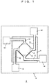
- Fig. 1 shows an example of MEMS gas sensors 2. It has a substrate 4 such as silicon and suitable for micro machining, and the substrate 4 has a cavity 6 that penetrates the substrate 4 and a support film 8 over the cavity 6 supported by, for example, four beams 12. On the support film 8, a film-like heater (not shown) and film-like electrodes (not shown) are formed, and a metal oxide semiconductor film 10 covers them.
- the metal oxide semiconductor film 10 is, for example, a thick film of SnO2 and may be other metal oxide semiconductor films such as In2O3, WO3, and so on. In addition, the metal oxide semiconductor film 10 may be a thin film. Further, both ends of the heater and ends of the electrodes are connected via the beams 12 to the pads 14.
- the support film 8 may be a diaphragm covering the cavity 6.
- the heater and the electrodes may be provided on the same layer, or alternatively, the heater may be covered by an insulating film and the electrodes may be provided on the insulating film. Further, without the electrodes, the parallel electrical resistance value of the metal oxide semiconductor and the heater may be detected.
- a catalytic layer may be provided over the metal oxide semiconductor film for eliminating unnecessary gases.
- a separate and independent filter from the substrate 4 may be provided in order for unnecessary gases to be adsorbed by the filter.
- Fig. 2 shows the gas sensor 2, a drive circuit 25 for the gas sensor, the main circuit board 26 of the mobile electronic device, and so on.
- Indicated by 16 is the heater of the gas sensor 2, by 18 the power supply such as a battery, by 20 the load resistor, and by 21,22 switches.
- a gas sensor drive 24 makes the switch 21 on and off in order to drive the heater 16, makes the switch 22 on and off, and measures the voltage over the load resistor 20 via an AD converter not shown. The voltage is determined by the electrical resistance of the metal oxide semiconductor 10. Gases are detected according to the voltage over the load resistor 20, relevant signal processing may be performed by the gas sensor drive 24 or by the main circuit board 26.
- the main circuit board 26 is the major portion of the mobile electronic device and communicates with the outside world through a communication unit 28. Further, the mobile electronic device is provided with an ambient light sensor 30 for detecting the ambient brightness, a proximity sensor 31 for detecting proximate objects such as a human body, a camera 32, a temperature sensor 32, an acceleration sensor 34, a magnetic sensor 35 for detecting terrestrial magnetism, and so on. Further, a touch panel 36, a speaker 37, a microphone 38, and so on are provided within the mobile electronic device.
- the gas sensor drive 24 needs the signal from the ambient light sensor 30 or the proximity sensor 31. While Fig.
- the gas sensor drive receives these signals from the main circuit board 26, it may directly receive the signal of the ambient light sensor 30 or the proximity sensor 31 via a bus (not shown).
- the drive circuit 25 indicates a circuit in the upper left portion in Fig. 2 except for the gas sensor 2 enclosed by a chain line.
- the power supply 18 is a common power supply for the entire mobile electronic device.
- the drive circuit 25 has a structure adapted for the connection with the main circuit board 26.
- Fig. 3 indicates the heater power or the heater voltage to the gas sensor 2 during the normal operation.
- the gas sensor 2 has an operation period Tc such as 10 seconds to 10 minutes.
- T1 such as 0.1 second to 1 second
- it is heated to a higher temperature (for example, 400 to 500°C) than the operating temperature (for example, 300 to 400°C), and then heated to the operating temperature for a time period T2 such as 1 second to 10 second.
- T2 such as 1 second to 10 second.
- the voltage over the load resistor is sampled, and the gas sensor drive 24 or the main circuit board 26 detects gases.
- the gas sensor 2 is kept at ambient temperatures.
- the operation period Tc may be shortened.
- the high-temperature heating during the period T1 may be omitted, and the temperature may be changed only between the ambient temperatures and the operating temperature.
- the timing for sampling the voltage over the load resistor is arbitrary.
- Fig. 4 indicates the algorithm for halting the operation of the heater when detecting the gas sensor 2, and therefore, the mobile electronic device are placed in a closed space.
- the gas sensor 2 is driven with the period Tc, and for example, the detection whether the mobile electronic device is placed in a closed space is performed for every period (step 1).
- a closed space means an enclosed space such as those within briefcases, handbags, pockets, drawers, and so on.
- the detection period of the closed space may be longer than the operation period Tc of the gas sensor 2.
- the ambient light sensor 30 may detect that the surrounding is dark and therefore, may detect that the mobile electronic device is placed in a closed space.
- the proximity sensor 31 detects an object always, this is a peculiar phenomenon to a closed space.
- the camera 32 may detect the brightness of the surroundings. While the type of sensors for detecting a closed space is arbitrary, a sensor installed within a mobile electronic device is used; a preferable sensor is the ambient light sensor 30 and the proximity sensor 31. As a remark, the ambient light sensor 30 may not distinguish a night time and a closed space. However, it is detectable, according to inputs to the touch panel 36 or the microphone 38, that the mobile electronic device is in operation by a user; when in usem the device may be estimated not in a closed space.
- the acceleration sensor 34 and the magnetic sensor 35 may detect that the mobile electronic device is placed in the same position for a long duration without being carried, and in this instance, the operation of the gas sensor 2 may be halted. In many cases, this means the owner of the device is in bed, and the detection of air quality in the bedroom is not important.
- the ambient light sensor 30 makes the operation of the gas sensor 2 halted when the owner is in bed. However, the proximity sensor 31 makes the operation of the gas sensor 2 continue when the owner is in bed.
- the target of the detection is that the gas sensor 2 is placed in a closed space for a duration longer than one operation period Tc.
- the detection of whether the device is placed in a closed space is performed plural times for one operation period Tc, and when all of the detections indicate a closed space, the gas sensor 2 (the mobile electronic device) is considered to be placed in a closed space.
- the gas sensor is considered to be kept in a closed space (step 2).
- step 3 When it is detected that the device is placed in a closed space, the operation of the gas sensor 2 is halted (step 3). Since the heater of the gas sensor 2 is not operated, the silicone gas adsorbed in the metal oxide semiconductor is prohibited from changing to compounds that are hardly to desorb by polymerization or the like. Further, a local convectional flow around the metal oxide semiconductor is prevented to occur, and therefore, the adsorption of silicone gases to the metal oxide semiconductor is reduced.
- organic solvents such as ethanol may contaminate MEMS gas sensors, and therefore, the contaminants are not limited to silicone gases.
- the duration when the operation is halted for example, the number of the operation periods Tc, is counted up (step 4). However, the halting duration may not be counted.
- the detection whether the device is placed in a closed space is performed for every operation period Tc, and when it is detected that the device has been taken out from a closed space (step 5), a heat-cleaning is performed in order to recover the gas response performance (step 6). Heating to 400 to 500°C for 30 seconds to 10 minutes is estimated enough long for making the adsorbed silicone gases desorb, even if some of them are polymerized. However, without the heat-cleaning, the gas sensor may be returned to normal operation shown in Fig. 3 upon the detection of open space.
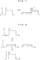
- Figs. 5 to 7 indicate examples of the heat-cleaning, where the left column indicates the normal operation pattern, and where the right column indicates the operation patterns with the heat-cleaning.
- the period for heating to the temperature higher than the operating temperature is extended from the normal period T1 to a heat-cleaning duration T3 of 30 seconds to 10 minutes.
- the metal oxide semiconductor is immediately heated to the operating temperature.
- the gas sensor 2 may be cooled to the ambient temperature and then it may be operated.
- the metal oxide semiconductor may experience a heat-cleaning at 80 to 200°C for a period T3, and various gases adsorbed when the operation of the gas sensor 2 was halted are vaporized.
- the heat-cleaning duration T3 is preferably determined, for example, according to the duration when the gas sensor 2 was placed in a closed space. For example, when the duration is relatively short (for example, from 10 minutes to 1 hour), heat-cleaning may be omitted, and when the duration is longer, the heat-cleaning period is preferably made longer.
- Fig. 9 when in contact with contaminant gases, the operation of the gas sensors 2 is halted; namely, the heater power is not added, and then the contamination is prevented.
- the heat-cleaning aims to remove various gases adsorbed when the operation of the gas sensors was halted. Therefore, the heat-cleaning may not be carried out.
- silicone or the like gases may be vaporized from the metal oxide semiconductor.
- Fig. 8 shows an example; when the gas sensor is placed in a closed space, the metal oxide semiconductor is heated to 80 to 200°C or a similar temperature for a period T4 with a predetermined interval, and as a result, the adsorbed silicone gases and so on are vaporized.
- the upper stage in the drawing indicates the normal operation pattern
- the middle stage indicates the operation pattern in a closed space
- the operation pattern is returned to the normal pattern when the gas sensor is taken out from a closed space.
- Fig. 9 indicates the difference in contamination between a case where the gas sensors 2 were operated in an environment including a silicone gas (the upper row) and a case where the operation of the gas sensors was halted in the environment including a silicone gas (the lower row).
- the gas sensors were placed in an atmosphere including 1 ppm of a siloxane gas (D5) for 24 hours; the siloxane concentration was higher than those in handbags or the like.
- the gas responses of the gas sensors before the siloxane contact are shown in the left column of Fig. 9 , and those after the siloxane contact are shown in the right column of Fig. 9 .
- gas responses to 3 ppm H2 were measured and then, gas responses to 10 ppm ethanol were measured.
- the operation pattern of the gas sensors was already indicated in Fig. 3 .
- the operation period Tc was 90 seconds, the period T1 was 1 second (the maximum temperature of the metal oxide semiconductor was about 400°C), the period T2 (the operation temperature of the metal oxide semiconductor was about 300°C) was 4 seconds.
- the metal oxide semiconductor was a thick film of SnO2 (the film thickness was about 20 micrometers).
- Fig. 9 shows the result when the gas sensors were continued to operate in the the silicone atmosphere and the lower row shows the result when the gas sensors were halted in the silicone atmosphere.
- the gas response characteristic was decreased in both the magnitude of the response and the speed of the response.
- the magnitude of the gas response was maintained at almost the same value and the speed of the response was maintained.
Landscapes
- Chemical & Material Sciences (AREA)
- Life Sciences & Earth Sciences (AREA)
- Health & Medical Sciences (AREA)
- Immunology (AREA)
- Pathology (AREA)
- Chemical Kinetics & Catalysis (AREA)
- General Physics & Mathematics (AREA)
- General Health & Medical Sciences (AREA)
- Biochemistry (AREA)
- Analytical Chemistry (AREA)
- Physics & Mathematics (AREA)
- Electrochemistry (AREA)
- Engineering & Computer Science (AREA)
- Computer Hardware Design (AREA)
- Microelectronics & Electronic Packaging (AREA)
- Medicinal Chemistry (AREA)
- Food Science & Technology (AREA)
- Combustion & Propulsion (AREA)
- Molecular Biology (AREA)
- Investigating Or Analyzing Materials By The Use Of Fluid Adsorption Or Reactions (AREA)
Applications Claiming Priority (2)
| Application Number | Priority Date | Filing Date | Title |
|---|---|---|---|
| JP2017003304 | 2017-01-12 | ||
| PCT/JP2017/047221 WO2018131503A1 (ja) | 2017-01-12 | 2017-12-28 | ガス検出装置とガス検出方法 |
Publications (3)
| Publication Number | Publication Date |
|---|---|
| EP3570018A1 true EP3570018A1 (de) | 2019-11-20 |
| EP3570018A4 EP3570018A4 (de) | 2020-10-28 |
| EP3570018B1 EP3570018B1 (de) | 2021-08-18 |
Family
ID=62839637
Family Applications (1)
| Application Number | Title | Priority Date | Filing Date |
|---|---|---|---|
| EP17890993.3A Active EP3570018B1 (de) | 2017-01-12 | 2017-12-28 | Gasdetektor und gasdetektionsverfahren |
Country Status (6)
| Country | Link |
|---|---|
| US (1) | US11385195B2 (de) |
| EP (1) | EP3570018B1 (de) |
| JP (1) | JP6864889B2 (de) |
| KR (1) | KR102252864B1 (de) |
| CN (1) | CN110178022B (de) |
| WO (1) | WO2018131503A1 (de) |
Families Citing this family (4)
| Publication number | Priority date | Publication date | Assignee | Title |
|---|---|---|---|---|
| JP6654712B2 (ja) * | 2017-02-03 | 2020-02-26 | 富士電機株式会社 | ガス警報器およびガス検出方法 |
| KR102641207B1 (ko) * | 2019-03-26 | 2024-02-28 | 엘지전자 주식회사 | 센서 모듈 |
| US12546759B2 (en) * | 2023-03-30 | 2026-02-10 | Saudi Arabian Oil Company | Thin polymer film dissolved under tension to detect hydrocarbon fuels hidden in paraffin-based lubrication oils |
| US12540909B2 (en) | 2023-12-29 | 2026-02-03 | Ge Infrastructure Technology Llc | Sensing system and method |
Family Cites Families (15)
| Publication number | Priority date | Publication date | Assignee | Title |
|---|---|---|---|---|
| JPS5529318A (en) | 1978-08-18 | 1980-03-01 | Satoru Nakayama | Fish and meat roasting instrument |
| GB2260648B (en) * | 1991-10-16 | 1995-05-17 | John Mfg Ltd | Sensor switch and a portable device sensitive to a change in movement |
| JP3830303B2 (ja) | 1999-05-28 | 2006-10-04 | 株式会社タニタ | 呼気成分測定機能を有する携帯電話機 |
| JP2009058389A (ja) * | 2007-08-31 | 2009-03-19 | New Cosmos Electric Corp | ガス検知素子 |
| JP2012172973A (ja) | 2011-02-17 | 2012-09-10 | Figaro Eng Inc | 可燃性ガス検出装置及び可燃性ガス検出方法 |
| JP5748211B2 (ja) * | 2011-05-26 | 2015-07-15 | フィガロ技研株式会社 | ガス検出装置とガス検出方法 |
| US8555701B1 (en) * | 2011-08-05 | 2013-10-15 | Cps Products, Inc. | Enhanced metal oxide gas sensor |
| US20130344609A1 (en) * | 2012-06-21 | 2013-12-26 | Felix Mayer | Chemical sensor in a portable electronic device |
| EP2762868B1 (de) * | 2013-01-31 | 2017-03-15 | Sensirion AG | Diffusionsbasierter Metalloxidgassensor |
| EP2763468B1 (de) * | 2013-01-31 | 2017-08-30 | Sensirion AG | Tragbare Sensorvorrichtung mit einem Gassensor und Verfahren zum Betrieb davon |
| EP2833128A1 (de) * | 2013-07-30 | 2015-02-04 | Sensirion AG | Integrierter chemischer Metalloxidsensor |
| KR102225031B1 (ko) * | 2014-01-14 | 2021-03-09 | 엘지전자 주식회사 | 단말기 및 그 동작 방법 |
| US20160189520A1 (en) * | 2014-12-31 | 2016-06-30 | Spec Sensors, Llc | Electronic Device Covers Having Gas Sensors |
| US9788277B2 (en) * | 2015-01-15 | 2017-10-10 | Mediatek Inc. | Power saving mechanism for in-pocket detection |
| CN104865851A (zh) * | 2015-03-20 | 2015-08-26 | 深圳市冠旭电子有限公司 | 一种根据光线变化的节能方法及装置 |
-
2017
- 2017-12-28 EP EP17890993.3A patent/EP3570018B1/de active Active
- 2017-12-28 JP JP2018561321A patent/JP6864889B2/ja active Active
- 2017-12-28 CN CN201780082478.5A patent/CN110178022B/zh not_active Expired - Fee Related
- 2017-12-28 KR KR1020197020916A patent/KR102252864B1/ko active Active
- 2017-12-28 US US16/469,356 patent/US11385195B2/en active Active
- 2017-12-28 WO PCT/JP2017/047221 patent/WO2018131503A1/ja not_active Ceased
Also Published As
| Publication number | Publication date |
|---|---|
| CN110178022A (zh) | 2019-08-27 |
| KR20190097204A (ko) | 2019-08-20 |
| JP6864889B2 (ja) | 2021-04-28 |
| CN110178022B (zh) | 2022-05-17 |
| KR102252864B1 (ko) | 2021-05-17 |
| US11385195B2 (en) | 2022-07-12 |
| EP3570018B1 (de) | 2021-08-18 |
| EP3570018A4 (de) | 2020-10-28 |
| WO2018131503A1 (ja) | 2018-07-19 |
| JPWO2018131503A1 (ja) | 2019-11-07 |
| US20190302046A1 (en) | 2019-10-03 |
Similar Documents
| Publication | Publication Date | Title |
|---|---|---|
| EP3570018B1 (de) | Gasdetektor und gasdetektionsverfahren | |
| US11977043B2 (en) | MEMS type semiconductor gas detection element | |
| US9651512B2 (en) | Gas sensor | |
| US11513092B2 (en) | Temperature-regulated gas sensor with gas selective filter | |
| Liess | Electric-field-induced migration of chemisorbed gas molecules on a sensitive film—a new chemical sensor | |
| KR20160023706A (ko) | 센서 조립체 작동 방법 | |
| WO2006096804A1 (en) | Temperature feedback control for solid state gas sensors | |
| US20190049398A1 (en) | Gas sensor, gas detection device, gas detection method and device provided with gas detection device | |
| Shin et al. | A wireless wearable sensor system based on a silver nanowire‐decorated silicon nanomembrane for precise and continuous hazardous gas monitoring | |
| EP3623805B1 (de) | Verfahren zum entgegenwirken von kontamination in gassensoren, zugehörige schaltung, vorrichtung und computerprogrammprodukt | |
| EP1220570A3 (de) | Anordnung zur Steuerung von elektrisch ansteuerbaren Geräten, insbesondere Elektrowärmegeräten | |
| KR20040111397A (ko) | 집적된 가스 센서 | |
| Das et al. | Enhanced response of co-planar MEMS microheater-based methane gas sensor | |
| JP6896679B2 (ja) | ガスセンサ | |
| EP2833129A1 (de) | Verfahren und Vorrichtung zur Analyse von Gasen durch einen auf Leitfähigkeit basierenden Partikulat-Metalloxid-Gassensor | |
| CN111094959B (zh) | 用于分析气体的方法和设备 | |
| Lang et al. | Long-term stability of a MEIS low energy hydrogen sensor | |
| Liess et al. | The modulation of thermoelectric power by chemisorption a new detection principle for microchip chemical sensors | |
| US20210270760A1 (en) | Gas detection device and gas detection method | |
| US11378537B2 (en) | Method of powering sensors, corresponding circuit and device | |
| Yeom et al. | A potentiostat-based wide-DR multi-sensor integrated interface for heterogeneous chemical sensor applications | |
| JP4016076B2 (ja) | ガス識別方法 | |
| JPH03185351A (ja) | ガス検出方法 | |
| Prieto et al. | Sensor readout circuit using AOSTFTs for IGZO (In-Ga-ZnO) sensors | |
| Sharma et al. | Design and development of multiple sensor array based on SnO 2 thin films for e-nose application |
Legal Events
| Date | Code | Title | Description |
|---|---|---|---|
| STAA | Information on the status of an ep patent application or granted ep patent |
Free format text: STATUS: THE INTERNATIONAL PUBLICATION HAS BEEN MADE |
|
| PUAI | Public reference made under article 153(3) epc to a published international application that has entered the european phase |
Free format text: ORIGINAL CODE: 0009012 |
|
| STAA | Information on the status of an ep patent application or granted ep patent |
Free format text: STATUS: REQUEST FOR EXAMINATION WAS MADE |
|
| 17P | Request for examination filed |
Effective date: 20190529 |
|
| AK | Designated contracting states |
Kind code of ref document: A1 Designated state(s): AL AT BE BG CH CY CZ DE DK EE ES FI FR GB GR HR HU IE IS IT LI LT LU LV MC MK MT NL NO PL PT RO RS SE SI SK SM TR |
|
| AX | Request for extension of the european patent |
Extension state: BA ME |
|
| DAV | Request for validation of the european patent (deleted) | ||
| DAX | Request for extension of the european patent (deleted) | ||
| A4 | Supplementary search report drawn up and despatched |
Effective date: 20200925 |
|
| RIC1 | Information provided on ipc code assigned before grant |
Ipc: G01N 27/12 20060101AFI20200921BHEP |
|
| GRAP | Despatch of communication of intention to grant a patent |
Free format text: ORIGINAL CODE: EPIDOSNIGR1 |
|
| STAA | Information on the status of an ep patent application or granted ep patent |
Free format text: STATUS: GRANT OF PATENT IS INTENDED |
|
| INTG | Intention to grant announced |
Effective date: 20210504 |
|
| RIN1 | Information on inventor provided before grant (corrected) |
Inventor name: OMORI AKIKO Inventor name: YOSHIOKA KENICHI |
|
| GRAS | Grant fee paid |
Free format text: ORIGINAL CODE: EPIDOSNIGR3 |
|
| GRAA | (expected) grant |
Free format text: ORIGINAL CODE: 0009210 |
|
| STAA | Information on the status of an ep patent application or granted ep patent |
Free format text: STATUS: THE PATENT HAS BEEN GRANTED |
|
| AK | Designated contracting states |
Kind code of ref document: B1 Designated state(s): AL AT BE BG CH CY CZ DE DK EE ES FI FR GB GR HR HU IE IS IT LI LT LU LV MC MK MT NL NO PL PT RO RS SE SI SK SM TR |
|
| REG | Reference to a national code |
Ref country code: GB Ref legal event code: FG4D |
|
| REG | Reference to a national code |
Ref country code: CH Ref legal event code: EP |
|
| REG | Reference to a national code |
Ref country code: DE Ref legal event code: R096 Ref document number: 602017044509 Country of ref document: DE |
|
| REG | Reference to a national code |
Ref country code: IE Ref legal event code: FG4D Ref country code: AT Ref legal event code: REF Ref document number: 1422085 Country of ref document: AT Kind code of ref document: T Effective date: 20210915 |
|
| REG | Reference to a national code |
Ref country code: LT Ref legal event code: MG9D |
|
| REG | Reference to a national code |
Ref country code: NL Ref legal event code: MP Effective date: 20210818 |
|
| REG | Reference to a national code |
Ref country code: AT Ref legal event code: MK05 Ref document number: 1422085 Country of ref document: AT Kind code of ref document: T Effective date: 20210818 |
|
| PG25 | Lapsed in a contracting state [announced via postgrant information from national office to epo] |
Ref country code: SE Free format text: LAPSE BECAUSE OF FAILURE TO SUBMIT A TRANSLATION OF THE DESCRIPTION OR TO PAY THE FEE WITHIN THE PRESCRIBED TIME-LIMIT Effective date: 20210818 Ref country code: RS Free format text: LAPSE BECAUSE OF FAILURE TO SUBMIT A TRANSLATION OF THE DESCRIPTION OR TO PAY THE FEE WITHIN THE PRESCRIBED TIME-LIMIT Effective date: 20210818 Ref country code: HR Free format text: LAPSE BECAUSE OF FAILURE TO SUBMIT A TRANSLATION OF THE DESCRIPTION OR TO PAY THE FEE WITHIN THE PRESCRIBED TIME-LIMIT Effective date: 20210818 Ref country code: FI Free format text: LAPSE BECAUSE OF FAILURE TO SUBMIT A TRANSLATION OF THE DESCRIPTION OR TO PAY THE FEE WITHIN THE PRESCRIBED TIME-LIMIT Effective date: 20210818 Ref country code: ES Free format text: LAPSE BECAUSE OF FAILURE TO SUBMIT A TRANSLATION OF THE DESCRIPTION OR TO PAY THE FEE WITHIN THE PRESCRIBED TIME-LIMIT Effective date: 20210818 Ref country code: PT Free format text: LAPSE BECAUSE OF FAILURE TO SUBMIT A TRANSLATION OF THE DESCRIPTION OR TO PAY THE FEE WITHIN THE PRESCRIBED TIME-LIMIT Effective date: 20211220 Ref country code: NO Free format text: LAPSE BECAUSE OF FAILURE TO SUBMIT A TRANSLATION OF THE DESCRIPTION OR TO PAY THE FEE WITHIN THE PRESCRIBED TIME-LIMIT Effective date: 20211118 Ref country code: BG Free format text: LAPSE BECAUSE OF FAILURE TO SUBMIT A TRANSLATION OF THE DESCRIPTION OR TO PAY THE FEE WITHIN THE PRESCRIBED TIME-LIMIT Effective date: 20211118 Ref country code: AT Free format text: LAPSE BECAUSE OF FAILURE TO SUBMIT A TRANSLATION OF THE DESCRIPTION OR TO PAY THE FEE WITHIN THE PRESCRIBED TIME-LIMIT Effective date: 20210818 Ref country code: LT Free format text: LAPSE BECAUSE OF FAILURE TO SUBMIT A TRANSLATION OF THE DESCRIPTION OR TO PAY THE FEE WITHIN THE PRESCRIBED TIME-LIMIT Effective date: 20210818 |
|
| PG25 | Lapsed in a contracting state [announced via postgrant information from national office to epo] |
Ref country code: PL Free format text: LAPSE BECAUSE OF FAILURE TO SUBMIT A TRANSLATION OF THE DESCRIPTION OR TO PAY THE FEE WITHIN THE PRESCRIBED TIME-LIMIT Effective date: 20210818 Ref country code: LV Free format text: LAPSE BECAUSE OF FAILURE TO SUBMIT A TRANSLATION OF THE DESCRIPTION OR TO PAY THE FEE WITHIN THE PRESCRIBED TIME-LIMIT Effective date: 20210818 Ref country code: GR Free format text: LAPSE BECAUSE OF FAILURE TO SUBMIT A TRANSLATION OF THE DESCRIPTION OR TO PAY THE FEE WITHIN THE PRESCRIBED TIME-LIMIT Effective date: 20211119 |
|
| PG25 | Lapsed in a contracting state [announced via postgrant information from national office to epo] |
Ref country code: NL Free format text: LAPSE BECAUSE OF FAILURE TO SUBMIT A TRANSLATION OF THE DESCRIPTION OR TO PAY THE FEE WITHIN THE PRESCRIBED TIME-LIMIT Effective date: 20210818 |
|
| PG25 | Lapsed in a contracting state [announced via postgrant information from national office to epo] |
Ref country code: DK Free format text: LAPSE BECAUSE OF FAILURE TO SUBMIT A TRANSLATION OF THE DESCRIPTION OR TO PAY THE FEE WITHIN THE PRESCRIBED TIME-LIMIT Effective date: 20210818 |
|
| REG | Reference to a national code |
Ref country code: DE Ref legal event code: R097 Ref document number: 602017044509 Country of ref document: DE |
|
| PG25 | Lapsed in a contracting state [announced via postgrant information from national office to epo] |
Ref country code: SM Free format text: LAPSE BECAUSE OF FAILURE TO SUBMIT A TRANSLATION OF THE DESCRIPTION OR TO PAY THE FEE WITHIN THE PRESCRIBED TIME-LIMIT Effective date: 20210818 Ref country code: SK Free format text: LAPSE BECAUSE OF FAILURE TO SUBMIT A TRANSLATION OF THE DESCRIPTION OR TO PAY THE FEE WITHIN THE PRESCRIBED TIME-LIMIT Effective date: 20210818 Ref country code: RO Free format text: LAPSE BECAUSE OF FAILURE TO SUBMIT A TRANSLATION OF THE DESCRIPTION OR TO PAY THE FEE WITHIN THE PRESCRIBED TIME-LIMIT Effective date: 20210818 Ref country code: EE Free format text: LAPSE BECAUSE OF FAILURE TO SUBMIT A TRANSLATION OF THE DESCRIPTION OR TO PAY THE FEE WITHIN THE PRESCRIBED TIME-LIMIT Effective date: 20210818 Ref country code: CZ Free format text: LAPSE BECAUSE OF FAILURE TO SUBMIT A TRANSLATION OF THE DESCRIPTION OR TO PAY THE FEE WITHIN THE PRESCRIBED TIME-LIMIT Effective date: 20210818 Ref country code: AL Free format text: LAPSE BECAUSE OF FAILURE TO SUBMIT A TRANSLATION OF THE DESCRIPTION OR TO PAY THE FEE WITHIN THE PRESCRIBED TIME-LIMIT Effective date: 20210818 |
|
| PLBE | No opposition filed within time limit |
Free format text: ORIGINAL CODE: 0009261 |
|
| STAA | Information on the status of an ep patent application or granted ep patent |
Free format text: STATUS: NO OPPOSITION FILED WITHIN TIME LIMIT |
|
| 26N | No opposition filed |
Effective date: 20220519 |
|
| PG25 | Lapsed in a contracting state [announced via postgrant information from national office to epo] |
Ref country code: MC Free format text: LAPSE BECAUSE OF FAILURE TO SUBMIT A TRANSLATION OF THE DESCRIPTION OR TO PAY THE FEE WITHIN THE PRESCRIBED TIME-LIMIT Effective date: 20210818 Ref country code: IT Free format text: LAPSE BECAUSE OF FAILURE TO SUBMIT A TRANSLATION OF THE DESCRIPTION OR TO PAY THE FEE WITHIN THE PRESCRIBED TIME-LIMIT Effective date: 20210818 |
|
| REG | Reference to a national code |
Ref country code: CH Ref legal event code: PL |
|
| PG25 | Lapsed in a contracting state [announced via postgrant information from national office to epo] |
Ref country code: SI Free format text: LAPSE BECAUSE OF FAILURE TO SUBMIT A TRANSLATION OF THE DESCRIPTION OR TO PAY THE FEE WITHIN THE PRESCRIBED TIME-LIMIT Effective date: 20210818 |
|
| REG | Reference to a national code |
Ref country code: BE Ref legal event code: MM Effective date: 20211231 |
|
| PG25 | Lapsed in a contracting state [announced via postgrant information from national office to epo] |
Ref country code: LU Free format text: LAPSE BECAUSE OF NON-PAYMENT OF DUE FEES Effective date: 20211228 Ref country code: IE Free format text: LAPSE BECAUSE OF NON-PAYMENT OF DUE FEES Effective date: 20211228 |
|
| PG25 | Lapsed in a contracting state [announced via postgrant information from national office to epo] |
Ref country code: BE Free format text: LAPSE BECAUSE OF NON-PAYMENT OF DUE FEES Effective date: 20211231 |
|
| PG25 | Lapsed in a contracting state [announced via postgrant information from national office to epo] |
Ref country code: LI Free format text: LAPSE BECAUSE OF NON-PAYMENT OF DUE FEES Effective date: 20211231 Ref country code: CH Free format text: LAPSE BECAUSE OF NON-PAYMENT OF DUE FEES Effective date: 20211231 |
|
| PGFP | Annual fee paid to national office [announced via postgrant information from national office to epo] |
Ref country code: GB Payment date: 20221229 Year of fee payment: 6 Ref country code: FR Payment date: 20221219 Year of fee payment: 6 Ref country code: DE Payment date: 20221213 Year of fee payment: 6 |
|
| PG25 | Lapsed in a contracting state [announced via postgrant information from national office to epo] |
Ref country code: CY Free format text: LAPSE BECAUSE OF FAILURE TO SUBMIT A TRANSLATION OF THE DESCRIPTION OR TO PAY THE FEE WITHIN THE PRESCRIBED TIME-LIMIT Effective date: 20210818 |
|
| PG25 | Lapsed in a contracting state [announced via postgrant information from national office to epo] |
Ref country code: HU Free format text: LAPSE BECAUSE OF FAILURE TO SUBMIT A TRANSLATION OF THE DESCRIPTION OR TO PAY THE FEE WITHIN THE PRESCRIBED TIME-LIMIT; INVALID AB INITIO Effective date: 20171228 |
|
| PG25 | Lapsed in a contracting state [announced via postgrant information from national office to epo] |
Ref country code: MK Free format text: LAPSE BECAUSE OF FAILURE TO SUBMIT A TRANSLATION OF THE DESCRIPTION OR TO PAY THE FEE WITHIN THE PRESCRIBED TIME-LIMIT Effective date: 20210818 |
|
| PG25 | Lapsed in a contracting state [announced via postgrant information from national office to epo] |
Ref country code: TR Free format text: LAPSE BECAUSE OF FAILURE TO SUBMIT A TRANSLATION OF THE DESCRIPTION OR TO PAY THE FEE WITHIN THE PRESCRIBED TIME-LIMIT Effective date: 20210818 |
|
| REG | Reference to a national code |
Ref country code: DE Ref legal event code: R119 Ref document number: 602017044509 Country of ref document: DE |
|
| GBPC | Gb: european patent ceased through non-payment of renewal fee |
Effective date: 20231228 |
|
| PG25 | Lapsed in a contracting state [announced via postgrant information from national office to epo] |
Ref country code: MT Free format text: LAPSE BECAUSE OF FAILURE TO SUBMIT A TRANSLATION OF THE DESCRIPTION OR TO PAY THE FEE WITHIN THE PRESCRIBED TIME-LIMIT Effective date: 20210818 |
|
| PG25 | Lapsed in a contracting state [announced via postgrant information from national office to epo] |
Ref country code: DE Free format text: LAPSE BECAUSE OF NON-PAYMENT OF DUE FEES Effective date: 20240702 |
|
| PG25 | Lapsed in a contracting state [announced via postgrant information from national office to epo] |
Ref country code: GB Free format text: LAPSE BECAUSE OF NON-PAYMENT OF DUE FEES Effective date: 20231228 |
|
| PG25 | Lapsed in a contracting state [announced via postgrant information from national office to epo] |
Ref country code: FR Free format text: LAPSE BECAUSE OF NON-PAYMENT OF DUE FEES Effective date: 20231231 |
|
| PG25 | Lapsed in a contracting state [announced via postgrant information from national office to epo] |
Ref country code: GB Free format text: LAPSE BECAUSE OF NON-PAYMENT OF DUE FEES Effective date: 20231228 Ref country code: FR Free format text: LAPSE BECAUSE OF NON-PAYMENT OF DUE FEES Effective date: 20231231 Ref country code: DE Free format text: LAPSE BECAUSE OF NON-PAYMENT OF DUE FEES Effective date: 20240702 |