EP3568706B1 - Apparatus for testing an optoelectronic device and method of operating the same - Google Patents
Apparatus for testing an optoelectronic device and method of operating the same Download PDFInfo
- Publication number
- EP3568706B1 EP3568706B1 EP18739026.5A EP18739026A EP3568706B1 EP 3568706 B1 EP3568706 B1 EP 3568706B1 EP 18739026 A EP18739026 A EP 18739026A EP 3568706 B1 EP3568706 B1 EP 3568706B1
- Authority
- EP
- European Patent Office
- Prior art keywords
- optoelectronic device
- thermal
- stage
- optoelectronic
- testing
- Prior art date
- Legal status (The legal status is an assumption and is not a legal conclusion. Google has not performed a legal analysis and makes no representation as to the accuracy of the status listed.)
- Active
Links
Images



Classifications
-
- G—PHYSICS
- G01—MEASURING; TESTING
- G01R—MEASURING ELECTRIC VARIABLES; MEASURING MAGNETIC VARIABLES
- G01R31/00—Arrangements for testing electric properties; Arrangements for locating electric faults; Arrangements for electrical testing characterised by what is being tested not provided for elsewhere
- G01R31/28—Testing of electronic circuits, e.g. by signal tracer
- G01R31/2851—Testing of integrated circuits [IC]
- G01R31/2855—Environmental, reliability or burn-in testing
- G01R31/2872—Environmental, reliability or burn-in testing related to electrical or environmental aspects, e.g. temperature, humidity, vibration, nuclear radiation
- G01R31/2874—Environmental, reliability or burn-in testing related to electrical or environmental aspects, e.g. temperature, humidity, vibration, nuclear radiation related to temperature
- G01R31/2875—Environmental, reliability or burn-in testing related to electrical or environmental aspects, e.g. temperature, humidity, vibration, nuclear radiation related to temperature related to heating
-
- G—PHYSICS
- G01—MEASURING; TESTING
- G01R—MEASURING ELECTRIC VARIABLES; MEASURING MAGNETIC VARIABLES
- G01R1/00—Details of instruments or arrangements of the types included in groups G01R5/00 - G01R13/00 and G01R31/00
- G01R1/02—General constructional details
- G01R1/04—Housings; Supporting members; Arrangements of terminals
- G01R1/0408—Test fixtures or contact fields; Connectors or connecting adaptors; Test clips; Test sockets
- G01R1/0433—Sockets for IC's or transistors
- G01R1/0441—Details
- G01R1/0458—Details related to environmental aspects, e.g. temperature
-
- G—PHYSICS
- G01—MEASURING; TESTING
- G01R—MEASURING ELECTRIC VARIABLES; MEASURING MAGNETIC VARIABLES
- G01R1/00—Details of instruments or arrangements of the types included in groups G01R5/00 - G01R13/00 and G01R31/00
- G01R1/02—General constructional details
- G01R1/04—Housings; Supporting members; Arrangements of terminals
- G01R1/0408—Test fixtures or contact fields; Connectors or connecting adaptors; Test clips; Test sockets
- G01R1/0433—Sockets for IC's or transistors
- G01R1/0441—Details
- G01R1/0466—Details concerning contact pieces or mechanical details, e.g. hinges or cams; Shielding
-
- G—PHYSICS
- G01—MEASURING; TESTING
- G01R—MEASURING ELECTRIC VARIABLES; MEASURING MAGNETIC VARIABLES
- G01R31/00—Arrangements for testing electric properties; Arrangements for locating electric faults; Arrangements for electrical testing characterised by what is being tested not provided for elsewhere
- G01R31/28—Testing of electronic circuits, e.g. by signal tracer
- G01R31/2851—Testing of integrated circuits [IC]
- G01R31/2855—Environmental, reliability or burn-in testing
- G01R31/2856—Internal circuit aspects, e.g. built-in test features; Test chips; Measuring material aspects, e.g. electro migration [EM]
-
- G—PHYSICS
- G01—MEASURING; TESTING
- G01R—MEASURING ELECTRIC VARIABLES; MEASURING MAGNETIC VARIABLES
- G01R31/00—Arrangements for testing electric properties; Arrangements for locating electric faults; Arrangements for electrical testing characterised by what is being tested not provided for elsewhere
- G01R31/28—Testing of electronic circuits, e.g. by signal tracer
- G01R31/2851—Testing of integrated circuits [IC]
- G01R31/2855—Environmental, reliability or burn-in testing
- G01R31/286—External aspects, e.g. related to chambers, contacting devices or handlers
- G01R31/2863—Contacting devices, e.g. sockets, burn-in boards or mounting fixtures
Definitions
- the optical performance of an optoelectronic device sometimes is measured at a number of different temperatures in order to evaluate performance of the device under different operating temperatures, and to evaluate whether the optoelectronic device is stable upon repeated exposure to non-ambient temperatures (i.e., thermal cycling).
- These tests can include directing the optoelectronic device to capture data of a test target (e.g., a grey card).
- a testing apparatus may include both the optoelectronic device and the test target.
- the entire apparatus is subjected to temperature changes in order to collect the test data from the optoelectronic device at the different temperatures.
- the optoelectronic device may be heated via convection by a heating element in close proximity to the optoelectronic device. This can result, however, in the entire apparatus being heated due inefficiencies in the method of heat transfer.
- Such a testing apparatus may have a number of problems. For example, as the temperature of the entire testing apparatus is altered, and the apparatus heat capacity is substantial, significant time may be required to reach a desired testing temperature. Further, sometimes the optoelectronic device is tested at elevated temperatures (e.g., 70°C). As the entire testing apparatus must be heated to an elevated temperature, the target also is heated to an elevated temperature. This can cause a number of issues. For example, as a single target may be used to evaluate multiple optoelectronic modules (e.g., 10s, 100s, or even 1000s), the target may exhibit dimensional changes with repeated testing such that the captured test data is inaccurate. Further, the test target may experience dimensional changes during testing (i.e., at an elevated temperature).
- elevated temperatures e.g. 70°C
- the target may exhibit dimensional changes with repeated testing such that the captured test data is inaccurate. Further, the test target may experience dimensional changes during testing (i.e., at an elevated temperature).
- test target may change chemically (e.g., the surface may oxidize), thereby generating spurious results.
- JP 2011 237350 relates to a light-emitting component test module
- US 2014/062513 relates to a thermal controller
- US 5911897 relates to a temperature control system for high power burn-in of integrated circuit chips.
- This disclosure describes apparatus for testing optoelectronic devices at multiple different temperatures that, in some cases, overcome the aforementioned challenges.
- the disclosure also describes methods for operating the apparatus.
- the apparatus can facilitate rapid optical performance measurements at multiple different temperatures.
- the test target can exhibit reduced degradation, thereby reducing or minimizing the collection of spurious measurement data.
- an apparatus for testing an optoelectronic device at multiple different temperatures includes an optoelectronic device stage, and a cavity disposed within the optoelectronic device stage.
- the cavity can be configured to accommodate the optoelectronic device such that the optoelectronic device is inset within the cavity.
- the apparatus further includes electrical contacts.
- the electrical contacts can be positioned at least partially within the optoelectronic device stage and can be operable to contact the optoelectronic device electrically.
- the electrical contacts can be operable to transmit testing commands and testing data between the optoelectronic device and a testing controller.
- the apparatus further includes a temperature sensing device.
- the temperature sensing device can be positioned within the stage proximal to the cavity and the optoelectronic device.
- the temperature sensing device can be operable to transmit temperature sensing data to a thermal controller.
- the apparatus further includes at least one spring fixedly connected to the optoelectronic device stage and a base. The spring(s) can be operable to bring the base and the optoelectronic device stage in thermal and mechanical communication.
- the apparatus further includes a thermal-adjustment device mounted proximal to the base and can be in thermal communication with the base.
- the thermal-adjustment device can be operable to exchange thermal energy with the base according to temperature adjustment data transmitted from the thermal controller.
- the apparatus further includes a target stage mounted proximal to the optoelectronic device stage. The target stage can be operable to mechanically contact the optoelectronic device.
- the apparatus further includes a target mounted within the target stage and aligned with the optoelectronic device.
- the apparatus for testing an optoelectronic device at different temperatures includes an optoelectronic device stage in thermal communication with the optoelectronic device.
- the thermal-adjustment device is a thermoelectric device.
- the thermal-adjustment device is a thermal heating element.
- the temperature-sensing device is a thermocouple.
- the temperature-sensing device is a thermistor.
- the apparatus for testing an optoelectronic device at different temperatures includes a fluid-filled thermal adjustment device mounted to a thermal adjustment device, the fluid-filled thermal adjustment device being in thermal communication with the thermal adjustment device.
- the apparatus for testing an optoelectronic device at different temperatures includes a heat sink mounted to a thermal adjustment device, the heat sink being in thermal communication with the thermal adjustment device.
- the heat sink is composed at least partially of aluminum.
- the heat sink is composed at least partially of copper.
- the electrical contacts are spring-loaded pins.
- the a cover glass is mounted within the target stage and is aligned with the optoelectronic device.
- the apparatus for testing an optoelectronic device at different temperatures includes a target stage and an optoelectronic device stage mounted forming a gas-tight seal around the optoelectronic device and a target.
- the apparatus for testing an optoelectronic device at different temperatures includes a channel operable to conduct gas between the cavity and an area external to the cavity.
- FIG. 1A An example apparatus 100 for testing an optoelectronic device at multiple different temperatures is depicted in FIG. 1A in an open position.
- the apparatus 100 includes an optoelectronic device 101.
- the optoelectronic device 101 includes an optoelectronic device stage 102 and a cavity 104 disposed within the optoelectronic device stage 102.
- the cavity 104 is configured to accommodate the optoelectronic device 101 such that the optoelectronic device 101 is inset within the cavity 104.
- the apparatus 100 further includes multiple electrical contacts 106.
- the electrical contacts 106 can be positioned at least partially within the optoelectronic device stage 102 and are operable to contact the optoelectronic device 101 electrically.
- the electrical contacts 106 are operable to transmit testing commands and testing data between the optoelectronic device and a testing controller.
- the electrical contacts 106 can be spring-loaded pins (pogo-pins), for example, or other adjustable electrical contacts.
- the apparatus 100 further includes a temperature sensing device 108.
- the temperature sensing device 108 can be positioned within the optoelectronic device stage 102 proximal to the cavity 104 and the optoelectronic device 101.
- the temperature sensing device 108 is operable to transmit temperature sensing data to a thermal controller such as a proportional-integral-derivative (PID) controller.
- PID proportional-integral-derivative
- the temperature sensing device 108 can be a thermocouple or a thermistor, for example.
- the apparatus 100 further includes at least one actuatable mechanical connector 110.
- the at least one actuatable mechanical connector 110 is fixedly connected to the optoelectronic device stage 102 and a base 112.
- the at least one actuatable mechanical connector 110 is operable to bring the base 112 and the optoelectronic device stage 102 in thermal and mechanical communication.
- the at least one actuatable mechanical connector 110 is a spring.
- the apparatus 100 further includes a thermal-adjustment device 114 mounted proximal to the base 112 and can be in thermal communication with the base 112.
- the thermal-adjustment device 114 is operable to exchange thermal energy with the base according to temperature adjustment data transmitted from the thermal controller.
- the thermal-adjustment device 114 can be a thermoelectric device or a thermal heating element, for example.
- the apparatus 100 further includes a heat sink 115 mounted to the thermal-adjustment device 114.
- the heat sink 115 is in thermal communication with the thermal adjustment device 114.
- the heat sink 115 can be at least partially composed of copper or aluminum, for example. In some instances, the heat sink 115 is at least partially composed of a high heat capacity material and/or a material with high thermal conductivity.
- the apparatus 100 further includes a target stage 116 mounted proximal to the optoelectronic device stage 102.
- the target stage 116 is operable to mechanically contact the optoelectronic device 101.
- the apparatus 100 further includes a target 118 mounted within the target stage 116 and aligned with the optoelectronic device 101 as indicated by alignment arrows Al as illustrated in FIG. 1A .
- the target can be a grey card, for example.
- FIG. 1B depicts the apparatus 100 for testing an optoelectronic device at different temperatures in a closed position.
- the apparatus 100 is illustrated with principal components in thermal and mechanical communication.
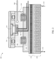
- FIG. 2 depicts another example of an apparatus for testing an optoelectronic device at multiple different temperatures.
- the apparatus 200 includes an optoelectronic device 201.
- the optoelectronic device 201 includes an optoelectronic device stage 202 and a cavity 204 disposed within the optoelectronic device stage 202.
- the cavity 204 is configured to accommodate the optoelectronic device 201 such that the optoelectronic device 201 is inset within the cavity 204.
- the apparatus 200 further includes electrical contacts 206.
- the electrical contacts 206 are positioned at least partially within the optoelectronic device stage 202 and are operable to contact the optoelectronic device 201 electrically.
- the electrical contacts 206 are operable to transmit testing commands and testing data between the optoelectronic device and a testing controller.
- the electrical contacts 206 can be spring-loaded pins (pogo-pins), for example, or other adjustable electrical contacts.
- the apparatus 200 further includes a temperature sensing device 208.
- the temperature sensing device 108 is positioned within the optoelectronic device stage 202 proximal to the cavity 204 and the optoelectronic device 201.
- the temperature sensing device 208 is operable to transmit temperature sensing data to a thermal controller such as a PID controller.
- the temperature sensing device 208 can be a thermocouple or a thermistor, for example.
- the apparatus 200 further includes at least one actuatable mechanical connector 210.
- the at least one actuatable mechanical connector 210 is fixedly connected to the optoelectronic device stage 202 and a base 212.
- the at least one actuatable mechanical connector 210 is operable to bring the base 212 and the optoelectronic device stage 202 in thermal and mechanical communication.
- the at least one actuatable mechanical connector 210 is a spring.
- the apparatus 200 further includes a thermal-adjustment device 214 mounted proximal to the base 212 and is in thermal communication with the base 212.
- the thermal-adjustment device 214 is operable to exchange thermal energy with the base according to temperature adjustment data transmitted from the thermal controller.
- the thermal-adjustment device 214 can be a thermoelectric device or a thermal heating element, for example.
- the apparatus 200 further includes a fluid-filled thermal adjustment device 220 with a fluid 222.
- the fluid-filled adjustment device 220 is mounted in thermal and mechanical communication with the thermal adjustment device 214.
- the fluid 222 can be water, ethelyne glycol, oil, air or any other suitable fluid operable to conduct heat from the vicinity of the thermal adjustment device 214 and further is operable to affect rapid temperature changes on the optoelectronic device 201.
- the apparatus 200 further includes a target stage 216 mounted proximal to the optoelectronic device stage 202.
- the target stage 216 is operable to mechanically contact the optoelectronic device 201.
- the apparatus 200 further includes a target 218 mounted within the target stage 216 and aligned with the optoelectronic device 201.
- the target can be a grey card, for example.
- FIG. 3 depicts still another example apparatus for testing an optoelectronic device at different temperatures.
- the apparatus 300 includes an optoelectronic device 301.
- the optoelectronic device 301 includes an optoelectronic device stage 302 and a cavity 304 disposed within the optoelectronic device stage 302.
- the cavity 304 is configured to accommodate the optoelectronic device 301 such that the optoelectronic device 301 is inset within the cavity 304.
- the apparatus 300 further includes a cover glass 324 aligned with the optoelectronic device 301.
- the cover glass 324 can simulate a cover glass with which the optoelectronic device 301 is likely to be aligned and mounted in operation (i.e., as implemented in an end-user's device).
- the apparatus 300 further includes electrical contacts 306.
- the electrical contacts 306 are positioned at least partially within the optoelectronic device stage 302 and are operable to contact the optoelectronic device 301 electrically.
- the electrical contacts 306 are operable to transmit testing commands and testing data between the optoelectronic device and a testing controller.
- the electrical contacts 306 can be spring-loaded pins (pogo-pins), for example, or other adjustable electrical contacts.
- the apparatus 300 further includes a temperature sensing device 308.
- the temperature sensing device 308 is positioned within the optoelectronic device stage 302 proximal to the cavity 304 and the optoelectronic device 301.
- the temperature sensing device 308 is operable to transmit temperature sensing data to a thermal controller such as a PID controller.
- the temperature sensing device 308 can be a thermocouple or a thermistor, for example.
- the apparatus 300 further includes at least one actuatable mechanical connector 310.
- the at least one actuatable mechanical connector 310 is fixedly connected to the optoelectronic device stage 302 and a base 312.
- the at least one actuatable mechanical connector 310 is operable to bring the base 312 and the optoelectronic device stage 302 in thermal and mechanical communication.
- the at least one actuatable mechanical connector 310 is a spring.
- the apparatus 300 further includes a thermal-adjustment device 314 mounted proximal to the base 312 and is in thermal communication with the base 312.
- the thermal-adjustment device 314 is operable to exchange thermal energy with the base according to temperature adjustment data transmitted from the thermal controller.
- the thermal-adjustment device 314 can be a thermoelectric device or a thermal heating element, for example.
- the apparatus 300 further includes a fluid-filled thermal adjustment device 320 with a fluid 322.
- the fluid-filled adjustment device 320 is mounted in thermal and mechanical communication with the thermal adjustment device 314.
- the fluid 322 can be water, ethylene glycol, oil, air or any other suitable fluid operable to conduct heat from the vicinity of the thermal adjustment device 314 and further is operable to affect rapid temperature changes on the optoelectronic device 301.
- the apparatus 300 further includes a target stage 316 mounted proximal to the optoelectronic device stage 302.
- the target stage 316 is operable to mechanically contact the optoelectronic device 301.
- the apparatus 300 further includes a target 318 mounted within the target stage 316 and aligned with the optoelectronic device 301.
- the target can be a grey card, for example.
- FIG. 4 depicts yet still another example apparatus for testing an optoelectronic device at different temperatures.
- the apparatus 400 includes an optoelectronic device 401.
- the optoelectronic device 401 includes an optoelectronic device stage 402 and a cavity 404 disposed within the optoelectronic device stage 402.
- the cavity 404 is configured to accommodate the optoelectronic device 401 such that the optoelectronic device 401 is inset within the cavity 404.
- the apparatus 400 further includes a cover glass 424 aligned with the optoelectronic device 401.
- the cover glass 424 can simulate a cover glass with which the optoelectronic device 401 is likely to be aligned and mounted in operation (i.e., as implemented in an end-user's device).
- the apparatus 400 further includes electrical contacts 406.
- the electrical contacts 406 are positioned at least partially within the optoelectronic device stage 402 and are operable to contact the optoelectronic device 401 electrically.
- the electrical contacts 406 are operable to transmit testing commands and testing data between the optoelectronic device and a testing controller.
- the electrical contacts 406 can be spring-loaded pins (pogo-pins), for example, or other adjustable electrical contacts.
- the apparatus 400 further includes a temperature sensing device 408.
- the temperature sensing device 408 is positioned within the optoelectronic device stage 402 proximal to the cavity 404 and the optoelectronic device 401.
- the temperature sensing device 408 is operable to transmit temperature sensing data to a thermal controller such as a PID controller.
- the temperature sensing device 408 can be a thermocouple or a thermistor, for example.
- the apparatus 400 further includes at least one actuatable mechanical connector 410.
- the at least one actuatable mechanical connector 410 is fixedly connected to the optoelectronic device stage 402 and a base 412.
- the at least one actuatable mechanical connector 410 is operable to bring the base 412 and the optoelectronic device stage 402 in thermal and mechanical communication.
- the at least one actuatable mechanical connector 410 is a spring.
- the apparatus 400 further includes a thermal-adjustment device 414 mounted proximal to the base 412 and is in thermal communication with the base 412.
- the thermal-adjustment device 414 is operable to exchange thermal energy with the base according to temperature adjustment data transmitted from the thermal controller.
- the thermal-adjustment device 414 is a thermoelectric device or a thermal heating element, for example.
- the apparatus 400 further includes a fluid-filled thermal adjustment device 420 with a fluid 422.
- the fluid-filled adjustment device 420 is mounted in thermal and mechanical communication with the thermal adjustment device 414.
- the fluid 422 can be water, ethylene glycol, oil, air or any other suitable fluid operable to conduct heat from the vicinity of the thermal adjustment device 414 and further operable to affect rapid temperature changes on the optoelectronic device 401.
- the apparatus 400 further includes a target stage 416 mounted proximal to the optoelectronic device stage 402.
- the target stage 416 is operable to mechanically contact the optoelectronic device 401.
- the apparatus 400 further includes a target 418 mounted within the target stage 416 and aligned with the optoelectronic device 401.
- the target can be a grey card, for example.
- the target stage 416 and the optoelectronic device stage 402 are mounted forming a gas-tight seal around the optoelectronic device 401 and the target 418.
- the apparatus 400 further includes an inert gas channel 426.
- the inert gas channel 426 is operable to conduct inert gas 428 between the cavity 404 and an area external to the cavity 404.
- inert gas 428 is argon or a reducing gas such as hydrogen or a mixture of gasses including hydrogen.
- the inert gas channel 426 is operable to evacuate the cavity 404.
- the humidity of the cavity 404 is altered via the inert gas channel 426.
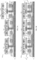
- FIG. 5A depicts an example apparatus for testing a plurality of optoelectronic devices at different temperatures.
- the apparatus 500A includes optoelectronic devices 501.
- the plurality of optoelectronic devices 501 include optoelectronic device stages 502A, 502B, 502C, and cavities 504A, 504B, 504C correspondingly disposed within each of the optoelectronic device stages 502A, 502B, 502C.
- the cavities 504A, 504B, 504C are configured to correspondingly accommodate the optoelectronic devices 501A, 501B, 501C such that the optoelectronic devices 501A, 501B, 501C are correspondingly inset within each of the cavities 504A, 504B, 504C.
- the apparatus 500A further includes electrical contacts 506.
- the electrical contacts 506 are positioned at least partially within each of the optoelectronic device stages 502A, 502B, 502C and are operable to correspondingly contact each of the optoelectronic devices 501A, 501B, 501C electrically.
- the electrical contacts 506 are operable to correspondingly transmit testing commands and testing data between each of the optoelectronic devices 501A, 501B, 501C and a testing controller.
- the electrical contacts 506 can be spring-loaded pins (pogo-pins), for example, or other adjustable electrical contacts.
- the apparatus 500A further includes temperature sensing devices 508A, 508B, 508C.
- Each of the temperature sensing devices 508A, 508B, 508C is positioned within a corresponding optoelectronic device stage 502A, 502B, 502C proximal to a corresponding cavity 504A, 504B, 504C and a corresponding optoelectronic device 501A, 501B, 501C.
- Each of the temperature sensing devices 508A, 508B, 508C is operable to transmit temperature sensing data to a thermal controller such as a PID controller.
- Each of the temperature sensing devices 508A, 508B, 508C can be a thermocouple or a thermistor, for example.
- the apparatus 500A further includes at least one actuatable mechanical connector 510A, 510B, 510C fixedly connected to a corresponding optoelectronic device stage 502A, 502B, 502C and a base 212.
- the at least one actuatable mechanical connector 510A, 510B, 510C are operable to bring the base 212 and a corresponding optoelectronic device stage 502A, 502B, 502C in thermal and mechanical communication.
- the at least one actuatable mechanical connectors 510A, 510B, 510C are springs.
- the apparatus 500A further includes a thermal-adjustment device 514 mounted proximal to the base 512 and in thermal communication with the base 512.
- the thermal-adjustment device 514 is operable to exchange thermal energy with the base according to temperature adjustment data transmitted from the thermal controller.
- the thermal-adjustment device 514 can be a thermoelectric device or a thermal heating element, for example.
- the apparatus 500A further includes target stages 516A, 516B, 516C correspondingly mounted proximal to the optoelectronic device stages 502A, 502B, 502C.
- the target stages 516A, 516B, 516C are operable to correspondingly mechanically contact the optoelectronic devices 501A, 501B, 501C.
- the apparatus 500A further includes targets 518A, 518B, 518C correspondingly mounted within the target stages 516A, 516B, 516C and correspondingly aligned with the optoelectronic devices 501A, 501B, 501C.
- the target can be a grey card, for example.
- FIG. 5B Another example apparatus for testing optoelectronic devices at different temperatures is depicted in FIG. 5B .
- the apparatus 500B includes optoelectronic devices 501.
- the optoelectronic devices 501 include optoelectronic device stages 502A, 502B, 502C, and cavities 504A, 504B, 504C correspondingly disposed within each of the optoelectronic device stages 502A, 502B, 502C.
- the cavities 504A, 504B, 504C are configured to correspondingly accommodate the optoelectronic devices 501A, 501B, 501C such that the optoelectronic devices 501A, 501B, 501C are correspondingly inset within each of the cavities 504A, 504B, 504C.
- the apparatus 500B further includes electrical contacts 506.
- the plurality of electrical contacts 506 are positioned at least partially within each of the optoelectronic device stages 502A, 502B, 502C and are operable to correspondingly contact each of the optoelectronic devices 501A, 501B, 501C electrically.
- the electrical contacts 506 are operable to correspondingly transmit testing commands and testing data between each of the optoelectronic devices 501A, 501B, 501C and a testing controller.
- the electrical contacts 506 can be spring-loaded pins (pogo-pins), for example, or other adjustable electrical contacts.
- the apparatus 500B further includes temperature sensing devices 508A, 508B, 508C.
- Each of the temperature sensing devices 508A, 508B, 508C is positioned within a corresponding optoelectronic device stage 502A, 502B, 502C proximal to a corresponding cavity 504A, 504B, 504C and a corresponding optoelectronic device 501A, 501B, 501C.
- Each of the temperature sensing devices 508A, 508B, 508C is operable to transmit temperature sensing data to a thermal controller such as a PID controller.
- Each of the temperature sensing devices 508A, 508B, 508C can be a thermocouple or a thermistor, for example.
- the apparatus 500B further includes at least one actuatable mechanical connector 510A, 510B, 510C fixedly connected to a corresponding optoelectronic device stage 502A, 502B, 502C and a base 212.
- the actuatable mechanical connectors 510A, 510B, 510C are operable to bring the base 212 and a corresponding optoelectronic device stage 502A, 502B, 502C in thermal and mechanical communication.
- the actuatable mechanical connectors 510A, 510B, 510C are springs.
- the apparatus 500B further includes a thermal-adjustment device 514 mounted proximal to the base 512 and in thermal communication with the base 512.
- the thermal-adjustment device 514 are operable to exchange thermal energy with the base according to temperature adjustment data transmitted from the thermal controller.
- the thermal-adjustment device 514 can be a thermoelectric device or a thermal heating element, for example.
- the apparatus 500B further includes a target stage 516 mounted proximal to the plurality of optoelectronic device stages 502A, 502B, 502C.
- the target stage 516 is operable to mechanically contact the optoelectronic devices 501A, 501B, 501C.
- the apparatus 500B further includes targets 518A, 518B, 518C mounted within the target stage 516 and correspondingly aligned with the optoelectronic devices 501A, 501B, 501C.
- the target can be a grey card, for example.
Landscapes
- Engineering & Computer Science (AREA)
- Physics & Mathematics (AREA)
- General Physics & Mathematics (AREA)
- Computer Hardware Design (AREA)
- Microelectronics & Electronic Packaging (AREA)
- Environmental & Geological Engineering (AREA)
- General Engineering & Computer Science (AREA)
- Toxicology (AREA)
- Health & Medical Sciences (AREA)
- Testing Of Individual Semiconductor Devices (AREA)
- Semiconductor Lasers (AREA)
- Testing Of Optical Devices Or Fibers (AREA)
- Investigating Or Analyzing Materials Using Thermal Means (AREA)
- Tests Of Electronic Circuits (AREA)
- Testing Resistance To Weather, Investigating Materials By Mechanical Methods (AREA)
Description
- The optical performance of an optoelectronic device sometimes is measured at a number of different temperatures in order to evaluate performance of the device under different operating temperatures, and to evaluate whether the optoelectronic device is stable upon repeated exposure to non-ambient temperatures (i.e., thermal cycling). These tests can include directing the optoelectronic device to capture data of a test target (e.g., a grey card). A testing apparatus may include both the optoelectronic device and the test target. In some instances, the entire apparatus is subjected to temperature changes in order to collect the test data from the optoelectronic device at the different temperatures. For example, the optoelectronic device may be heated via convection by a heating element in close proximity to the optoelectronic device. This can result, however, in the entire apparatus being heated due inefficiencies in the method of heat transfer.
- Such a testing apparatus may have a number of problems. For example, as the temperature of the entire testing apparatus is altered, and the apparatus heat capacity is substantial, significant time may be required to reach a desired testing temperature. Further, sometimes the optoelectronic device is tested at elevated temperatures (e.g., 70°C). As the entire testing apparatus must be heated to an elevated temperature, the target also is heated to an elevated temperature. This can cause a number of issues. For example, as a single target may be used to evaluate multiple optoelectronic modules (e.g., 10s, 100s, or even 1000s), the target may exhibit dimensional changes with repeated testing such that the captured test data is inaccurate. Further, the test target may experience dimensional changes during testing (i.e., at an elevated temperature). Further, the test target may change chemically (e.g., the surface may oxidize), thereby generating spurious results.
US 2005/206368 relates to an integrated circuit package testing apparatus,JP 2011 237350 US 2014/062513 relates to a thermal controller, andUS 5911897 relates to a temperature control system for high power burn-in of integrated circuit chips. - This disclosure describes apparatus for testing optoelectronic devices at multiple different temperatures that, in some cases, overcome the aforementioned challenges. The disclosure also describes methods for operating the apparatus. The apparatus can facilitate rapid optical performance measurements at multiple different temperatures. Moreover, the test target can exhibit reduced degradation, thereby reducing or minimizing the collection of spurious measurement data.
- In a first aspect, an apparatus for testing an optoelectronic device at multiple different temperatures includes an optoelectronic device stage, and a cavity disposed within the optoelectronic device stage. The cavity can be configured to accommodate the optoelectronic device such that the optoelectronic device is inset within the cavity. The apparatus further includes electrical contacts. The electrical contacts can be positioned at least partially within the optoelectronic device stage and can be operable to contact the optoelectronic device electrically. The electrical contacts can be operable to transmit testing commands and testing data between the optoelectronic device and a testing controller. The apparatus further includes a temperature sensing device. The temperature sensing device can be positioned within the stage proximal to the cavity and the optoelectronic device. The temperature sensing device can be operable to transmit temperature sensing data to a thermal controller. The apparatus further includes at least one spring fixedly connected to the optoelectronic device stage and a base. The spring(s) can be operable to bring the base and the optoelectronic device stage in thermal and mechanical communication. The apparatus further includes a thermal-adjustment device mounted proximal to the base and can be in thermal communication with the base. The thermal-adjustment device can be operable to exchange thermal energy with the base according to temperature adjustment data transmitted from the thermal controller. The apparatus further includes a target stage mounted proximal to the optoelectronic device stage. The target stage can be operable to mechanically contact the optoelectronic device. The apparatus further includes a target mounted within the target stage and aligned with the optoelectronic device.
- In some implementations, the apparatus for testing an optoelectronic device at different temperatures includes an optoelectronic device stage in thermal communication with the optoelectronic device.
- In some implementations, the thermal-adjustment device is a thermoelectric device.
- In some implementations, the thermal-adjustment device is a thermal heating element.
- In some implementations, the temperature-sensing device is a thermocouple.
- In some implementations, the temperature-sensing device is a thermistor.
- In some instances, the apparatus for testing an optoelectronic device at different temperatures includes a fluid-filled thermal adjustment device mounted to a thermal adjustment device, the fluid-filled thermal adjustment device being in thermal communication with the thermal adjustment device.
- In some cases, the apparatus for testing an optoelectronic device at different temperatures includes a heat sink mounted to a thermal adjustment device, the heat sink being in thermal communication with the thermal adjustment device.
- In some implementations, the heat sink is composed at least partially of aluminum.
- In some instances, the heat sink is composed at least partially of copper.
- In some implementations, the electrical contacts are spring-loaded pins.
- In some implementations, the a cover glass is mounted within the target stage and is aligned with the optoelectronic device.
- In some implementations, the apparatus for testing an optoelectronic device at different temperatures includes a target stage and an optoelectronic device stage mounted forming a gas-tight seal around the optoelectronic device and a target.
- In some implementations, the apparatus for testing an optoelectronic device at different temperatures includes a channel operable to conduct gas between the cavity and an area external to the cavity.
- Other aspects, features and advantages will be readily apparent from the following detailed description, the accompanying drawings, and the claims.
-
-
FIG. 1A depicts an example of an apparatus, in an open position, for testing an optoelectronic device at different temperatures. -
FIG. 1B depicts the apparatus depicted inFIG. 1A in a closed position. -
FIG. 2 depicts another example of an apparatus for testing an optoelectronic device at different temperatures. -
FIG. 3 depicts still another example of an apparatus for testing an optoelectronic device at different temperatures. -
FIG. 4 depicts yet still another example of an apparatus for testing an optoelectronic device at different temperatures. -
FIG. 5A depicts an example of an apparatus for testing multiple optoelectronic devices at different temperatures. -
FIG. 5B depicts another example of an apparatus for testing multiple optoelectronic devices at different temperatures. - An example apparatus 100 for testing an optoelectronic device at multiple different temperatures is depicted in
FIG. 1A in an open position. The apparatus 100 includes anoptoelectronic device 101. Theoptoelectronic device 101 includes anoptoelectronic device stage 102 and acavity 104 disposed within theoptoelectronic device stage 102. Thecavity 104 is configured to accommodate theoptoelectronic device 101 such that theoptoelectronic device 101 is inset within thecavity 104. - The apparatus 100 further includes multiple
electrical contacts 106. Theelectrical contacts 106 can be positioned at least partially within theoptoelectronic device stage 102 and are operable to contact theoptoelectronic device 101 electrically. Theelectrical contacts 106 are operable to transmit testing commands and testing data between the optoelectronic device and a testing controller. Theelectrical contacts 106 can be spring-loaded pins (pogo-pins), for example, or other adjustable electrical contacts. - The apparatus 100 further includes a
temperature sensing device 108. Thetemperature sensing device 108 can be positioned within theoptoelectronic device stage 102 proximal to thecavity 104 and theoptoelectronic device 101. Thetemperature sensing device 108 is operable to transmit temperature sensing data to a thermal controller such as a proportional-integral-derivative (PID) controller. Thetemperature sensing device 108 can be a thermocouple or a thermistor, for example. - The apparatus 100 further includes at least one actuatable
mechanical connector 110. The at least one actuatablemechanical connector 110 is fixedly connected to theoptoelectronic device stage 102 and abase 112. The at least one actuatablemechanical connector 110 is operable to bring thebase 112 and theoptoelectronic device stage 102 in thermal and mechanical communication. In some instances, the at least one actuatablemechanical connector 110 is a spring. - The apparatus 100 further includes a thermal-
adjustment device 114 mounted proximal to thebase 112 and can be in thermal communication with thebase 112. The thermal-adjustment device 114 is operable to exchange thermal energy with the base according to temperature adjustment data transmitted from the thermal controller. The thermal-adjustment device 114 can be a thermoelectric device or a thermal heating element, for example. - The apparatus 100 further includes a
heat sink 115 mounted to the thermal-adjustment device 114. Theheat sink 115 is in thermal communication with thethermal adjustment device 114. Theheat sink 115 can be at least partially composed of copper or aluminum, for example. In some instances, theheat sink 115 is at least partially composed of a high heat capacity material and/or a material with high thermal conductivity. - The apparatus 100 further includes a
target stage 116 mounted proximal to theoptoelectronic device stage 102. Thetarget stage 116 is operable to mechanically contact theoptoelectronic device 101. - The apparatus 100 further includes a
target 118 mounted within thetarget stage 116 and aligned with theoptoelectronic device 101 as indicated by alignment arrows Al as illustrated inFIG. 1A . The target can be a grey card, for example. -
FIG. 1B depicts the apparatus 100 for testing an optoelectronic device at different temperatures in a closed position. The apparatus 100 is illustrated with principal components in thermal and mechanical communication. -
FIG. 2 depicts another example of an apparatus for testing an optoelectronic device at multiple different temperatures. Theapparatus 200 includes an optoelectronic device 201. The optoelectronic device 201 includes anoptoelectronic device stage 202 and a cavity 204 disposed within theoptoelectronic device stage 202. The cavity 204 is configured to accommodate the optoelectronic device 201 such that the optoelectronic device 201 is inset within the cavity 204. - The
apparatus 200 further includeselectrical contacts 206. Theelectrical contacts 206 are positioned at least partially within theoptoelectronic device stage 202 and are operable to contact the optoelectronic device 201 electrically. Theelectrical contacts 206 are operable to transmit testing commands and testing data between the optoelectronic device and a testing controller. Theelectrical contacts 206 can be spring-loaded pins (pogo-pins), for example, or other adjustable electrical contacts. - The
apparatus 200 further includes atemperature sensing device 208. Thetemperature sensing device 108 is positioned within theoptoelectronic device stage 202 proximal to the cavity 204 and the optoelectronic device 201. Thetemperature sensing device 208 is operable to transmit temperature sensing data to a thermal controller such as a PID controller. Thetemperature sensing device 208 can be a thermocouple or a thermistor, for example. - The
apparatus 200 further includes at least one actuatablemechanical connector 210. The at least one actuatablemechanical connector 210 is fixedly connected to theoptoelectronic device stage 202 and abase 212. The at least one actuatablemechanical connector 210 is operable to bring thebase 212 and theoptoelectronic device stage 202 in thermal and mechanical communication. The at least one actuatablemechanical connector 210 is a spring. - The
apparatus 200 further includes a thermal-adjustment device 214 mounted proximal to thebase 212 and is in thermal communication with thebase 212. The thermal-adjustment device 214 is operable to exchange thermal energy with the base according to temperature adjustment data transmitted from the thermal controller. The thermal-adjustment device 214 can be a thermoelectric device or a thermal heating element, for example. - The
apparatus 200 further includes a fluid-filledthermal adjustment device 220 with afluid 222. The fluid-filledadjustment device 220 is mounted in thermal and mechanical communication with thethermal adjustment device 214. The fluid 222 can be water, ethelyne glycol, oil, air or any other suitable fluid operable to conduct heat from the vicinity of thethermal adjustment device 214 and further is operable to affect rapid temperature changes on the optoelectronic device 201. - The
apparatus 200 further includes atarget stage 216 mounted proximal to theoptoelectronic device stage 202. Thetarget stage 216 is operable to mechanically contact the optoelectronic device 201. - The
apparatus 200 further includes atarget 218 mounted within thetarget stage 216 and aligned with the optoelectronic device 201. The target can be a grey card, for example. -
FIG. 3 depicts still another example apparatus for testing an optoelectronic device at different temperatures. Theapparatus 300 includes an optoelectronic device 301. The optoelectronic device 301 includes anoptoelectronic device stage 302 and a cavity 304 disposed within theoptoelectronic device stage 302. The cavity 304 is configured to accommodate the optoelectronic device 301 such that the optoelectronic device 301 is inset within the cavity 304. Theapparatus 300 further includes acover glass 324 aligned with the optoelectronic device 301. Thecover glass 324 can simulate a cover glass with which the optoelectronic device 301 is likely to be aligned and mounted in operation (i.e., as implemented in an end-user's device). - The
apparatus 300 further includeselectrical contacts 306. Theelectrical contacts 306 are positioned at least partially within theoptoelectronic device stage 302 and are operable to contact the optoelectronic device 301 electrically. Theelectrical contacts 306 are operable to transmit testing commands and testing data between the optoelectronic device and a testing controller. Theelectrical contacts 306 can be spring-loaded pins (pogo-pins), for example, or other adjustable electrical contacts. - The
apparatus 300 further includes atemperature sensing device 308. Thetemperature sensing device 308 is positioned within theoptoelectronic device stage 302 proximal to the cavity 304 and the optoelectronic device 301. Thetemperature sensing device 308 is operable to transmit temperature sensing data to a thermal controller such as a PID controller. Thetemperature sensing device 308 can be a thermocouple or a thermistor, for example. - The
apparatus 300 further includes at least one actuatablemechanical connector 310. The at least one actuatablemechanical connector 310 is fixedly connected to theoptoelectronic device stage 302 and abase 312. The at least one actuatablemechanical connector 310 is operable to bring thebase 312 and theoptoelectronic device stage 302 in thermal and mechanical communication. The at least one actuatablemechanical connector 310 is a spring. - The
apparatus 300 further includes a thermal-adjustment device 314 mounted proximal to thebase 312 and is in thermal communication with thebase 312. The thermal-adjustment device 314 is operable to exchange thermal energy with the base according to temperature adjustment data transmitted from the thermal controller. The thermal-adjustment device 314 can be a thermoelectric device or a thermal heating element, for example. - The
apparatus 300 further includes a fluid-filledthermal adjustment device 320 with afluid 322. The fluid-filledadjustment device 320 is mounted in thermal and mechanical communication with thethermal adjustment device 314. The fluid 322 can be water, ethylene glycol, oil, air or any other suitable fluid operable to conduct heat from the vicinity of thethermal adjustment device 314 and further is operable to affect rapid temperature changes on the optoelectronic device 301. - The
apparatus 300 further includes atarget stage 316 mounted proximal to theoptoelectronic device stage 302. Thetarget stage 316 is operable to mechanically contact the optoelectronic device 301. - The
apparatus 300 further includes atarget 318 mounted within thetarget stage 316 and aligned with the optoelectronic device 301. The target can be a grey card, for example. -
FIG. 4 depicts yet still another example apparatus for testing an optoelectronic device at different temperatures. Theapparatus 400 includes an optoelectronic device 401. The optoelectronic device 401 includes anoptoelectronic device stage 402 and a cavity 404 disposed within theoptoelectronic device stage 402. The cavity 404 is configured to accommodate the optoelectronic device 401 such that the optoelectronic device 401 is inset within the cavity 404. Theapparatus 400 further includes acover glass 424 aligned with the optoelectronic device 401. Thecover glass 424 can simulate a cover glass with which the optoelectronic device 401 is likely to be aligned and mounted in operation (i.e., as implemented in an end-user's device). - The
apparatus 400 further includeselectrical contacts 406. Theelectrical contacts 406 are positioned at least partially within theoptoelectronic device stage 402 and are operable to contact the optoelectronic device 401 electrically. Theelectrical contacts 406 are operable to transmit testing commands and testing data between the optoelectronic device and a testing controller. Theelectrical contacts 406 can be spring-loaded pins (pogo-pins), for example, or other adjustable electrical contacts. - The
apparatus 400 further includes atemperature sensing device 408. Thetemperature sensing device 408 is positioned within theoptoelectronic device stage 402 proximal to the cavity 404 and the optoelectronic device 401. Thetemperature sensing device 408 is operable to transmit temperature sensing data to a thermal controller such as a PID controller. Thetemperature sensing device 408 can be a thermocouple or a thermistor, for example. - The
apparatus 400 further includes at least one actuatablemechanical connector 410. The at least one actuatablemechanical connector 410 is fixedly connected to theoptoelectronic device stage 402 and abase 412. The at least one actuatablemechanical connector 410 is operable to bring thebase 412 and theoptoelectronic device stage 402 in thermal and mechanical communication. The at least one actuatablemechanical connector 410 is a spring. - The
apparatus 400 further includes a thermal-adjustment device 414 mounted proximal to thebase 412 and is in thermal communication with thebase 412. The thermal-adjustment device 414 is operable to exchange thermal energy with the base according to temperature adjustment data transmitted from the thermal controller. The thermal-adjustment device 414 is a thermoelectric device or a thermal heating element, for example. - The
apparatus 400 further includes a fluid-filledthermal adjustment device 420 with afluid 422. The fluid-filledadjustment device 420 is mounted in thermal and mechanical communication with thethermal adjustment device 414. The fluid 422 can be water, ethylene glycol, oil, air or any other suitable fluid operable to conduct heat from the vicinity of thethermal adjustment device 414 and further operable to affect rapid temperature changes on the optoelectronic device 401. - The
apparatus 400 further includes a target stage 416 mounted proximal to theoptoelectronic device stage 402. The target stage 416 is operable to mechanically contact the optoelectronic device 401. - The
apparatus 400 further includes atarget 418 mounted within the target stage 416 and aligned with the optoelectronic device 401. The target can be a grey card, for example. In some instances, the target stage 416 and theoptoelectronic device stage 402 are mounted forming a gas-tight seal around the optoelectronic device 401 and thetarget 418. - The
apparatus 400 further includes aninert gas channel 426. Theinert gas channel 426 is operable to conductinert gas 428 between the cavity 404 and an area external to the cavity 404. In some instances,inert gas 428 is argon or a reducing gas such as hydrogen or a mixture of gasses including hydrogen. In some instances, theinert gas channel 426 is operable to evacuate the cavity 404. In some instances, the humidity of the cavity 404 is altered via theinert gas channel 426. -
FIG. 5A depicts an example apparatus for testing a plurality of optoelectronic devices at different temperatures. Theapparatus 500A includes optoelectronic devices 501. The plurality of optoelectronic devices 501 include optoelectronic device stages 502A, 502B, 502C, and cavities 504A, 504B, 504C correspondingly disposed within each of the optoelectronic device stages 502A, 502B, 502C. The cavities 504A, 504B, 504C are configured to correspondingly accommodate theoptoelectronic devices optoelectronic devices - The
apparatus 500A further includes electrical contacts 506. The electrical contacts 506 are positioned at least partially within each of the optoelectronic device stages 502A, 502B, 502C and are operable to correspondingly contact each of theoptoelectronic devices optoelectronic devices - The
apparatus 500A further includestemperature sensing devices temperature sensing devices optoelectronic device stage optoelectronic device temperature sensing devices temperature sensing devices - The
apparatus 500A further includes at least one actuatablemechanical connector optoelectronic device stage base 212. The at least one actuatablemechanical connector base 212 and a correspondingoptoelectronic device stage mechanical connectors - The
apparatus 500A further includes a thermal-adjustment device 514 mounted proximal to thebase 512 and in thermal communication with thebase 512. The thermal-adjustment device 514 is operable to exchange thermal energy with the base according to temperature adjustment data transmitted from the thermal controller. The thermal-adjustment device 514 can be a thermoelectric device or a thermal heating element, for example. - The
apparatus 500A further includes target stages 516A, 516B, 516C correspondingly mounted proximal to the optoelectronic device stages 502A, 502B, 502C. The target stages 516A, 516B, 516C are operable to correspondingly mechanically contact theoptoelectronic devices - The
apparatus 500A further includestargets optoelectronic devices - Another example apparatus for testing optoelectronic devices at different temperatures is depicted in
FIG. 5B . Theapparatus 500B includes optoelectronic devices 501. The optoelectronic devices 501 include optoelectronic device stages 502A, 502B, 502C, and cavities 504A, 504B, 504C correspondingly disposed within each of the optoelectronic device stages 502A, 502B, 502C. The cavities 504A, 504B, 504C are configured to correspondingly accommodate theoptoelectronic devices optoelectronic devices - The
apparatus 500B further includes electrical contacts 506. The plurality of electrical contacts 506 are positioned at least partially within each of the optoelectronic device stages 502A, 502B, 502C and are operable to correspondingly contact each of theoptoelectronic devices optoelectronic devices - The
apparatus 500B further includestemperature sensing devices temperature sensing devices optoelectronic device stage optoelectronic device temperature sensing devices temperature sensing devices - The
apparatus 500B further includes at least one actuatablemechanical connector optoelectronic device stage base 212. The actuatablemechanical connectors base 212 and a correspondingoptoelectronic device stage mechanical connectors - The
apparatus 500B further includes a thermal-adjustment device 514 mounted proximal to thebase 512 and in thermal communication with thebase 512. The thermal-adjustment device 514 are operable to exchange thermal energy with the base according to temperature adjustment data transmitted from the thermal controller. The thermal-adjustment device 514 can be a thermoelectric device or a thermal heating element, for example. - The
apparatus 500B further includes a target stage 516 mounted proximal to the plurality of optoelectronic device stages 502A, 502B, 502C. The target stage 516 is operable to mechanically contact theoptoelectronic devices - The
apparatus 500B further includestargets optoelectronic devices - The invention is defined by the appended claims.
Claims (14)
- An apparatus (100, 200, 300, 400, 500) for testing an optoelectronic device at a plurality of different temperatures, the apparatus comprising:an optoelectronic device stage (102, 202, 302, 402, 502);a cavity (104, 204, 304, 404) disposed within the optoelectronic device stage (102, 202, 302, 402, 502), the cavity (104, 204, 304, 404) being configured to accommodate the optoelectronic device such that the optoelectronic device is inset within the cavity (104, 204, 304, 404);a plurality of electrical contacts (106, 206, 306, 406, 506) positioned at least partially within the optoelectronic device stage (102, 202, 302, 402, 502) and operable to contact the optoelectronic device electrically, wherein the plurality of electrical contacts (106, 206, 306, 406, 506) are operable to transmit testing commands and testing data between the optoelectronic device and a testing controller;a temperature sensing device (108, 208, 308, 408, 508) positioned within the optoelectronic device stage (102, 202, 302, 402, 502) proximal to the cavity (104, 204, 304, 404) and the optoelectronic device, wherein the temperature sensing device (108, 208, 308, 408, 508)is operable to transmit temperature sensing data to a thermal controller;at least one spring (110, 210, 310, 410, 510) fixedly connected to the optoelectronic device stage (102, 202, 302, 402, 502) and a base (112, 212, 312, 412, 512), the at least one spring (110, 210, 310, 410, 510) being operable to bring the base (112, 212, 312, 412, 512) and the optoelectronic device stage (102, 202, 302, 402, 502) in thermal and mechanical communication;a thermal-adjustment device (114, 214, 314) mounted proximal to the base (112, 212, 312, 412, 512) and in thermal communication with the base (112, 212, 312, 412, 512), the thermal-adjustment device (114, 214, 314) being operable to exchange thermal energy with the base (112, 212, 312, 412, 512) according to temperature adjustment data transmitted from the thermal controller;a target stage (116, 216, 316, 416, 516) mounted proximal to the optoelectronic device stage (102, 202, 302, 402, 502)and operable to mechanically contact the optoelectronic device; anda target (118, 218, 318, 418) mounted within the target stage (116, 216, 316, 416, 516) and aligned with the optoelectronic device.
- The apparatus of claim 1, wherein the optoelectronic device stage (102, 202, 302, 402, 502) is in thermal communication with the optoelectronic device.
- The apparatus of claim 1, wherein the thermal-adjustment device (114, 214, 314) is a thermoelectric device.
- The apparatus of claim 1, wherein the thermal-adjustment device (114, 214, 314) is a thermal heating element.
- The apparatus of claim 1, wherein the temperature-sensing device (108, 208, 308, 408, 508) is a thermocouple.
- The apparatus of claim 1, wherein the temperature-sensing device (108, 208, 308, 408, 508) is a thermistor.
- The apparatus of claim 1 further comprising a fluid-filled thermal adjustment device (220, 320) mounted to the thermal adjustment device (214, 314), the fluid-filled thermal adjustment device (220, 320) being in thermal communication with the thermal adjustment device (214, 314).
- The apparatus of claim 1 further comprising a heat sink (115) mounted to the thermal adjustment device (114), the heat sink (115) being in thermal communication with the thermal adjustment device (114).
- The apparatus of claim 8, wherein the heat sink (115) is composed either at least partially of aluminum or at least partially of copper.
- The apparatus of claim 1, wherein the plurality of electrical contacts (106, 206, 306, 406, 506) include spring-loaded pins.
- The apparatus of claim 1, wherein the target stage (316, 416) further includes a cover glass (324, 424) mounted within the target stage (316, 416) and aligned with the optoelectronic device.
- The apparatus of claim 1, wherein the target stage (416) and the optoelectronic device stage (402) are mounted to form a gas-tight seal around the optoelectronic device and the target (418).
- The apparatus of claim 12 further including a channel (426) operable to conduct gas between the cavity (404) and an area external to the cavity (404).
- A method for testing an optoelectronic device, comprising:providing an apparatus (100, 200, 300, 400, 500) for testing the optoelectronic device as defined in claims 1-13, the apparatus including an optoelectronic device stage (102, 202, 302, 402, 502);mounting the optoelectronic device into a cavity (104, 204, 304, 404) within the optoelectronic device stage (102, 202, 302, 402, 502);contacting the optoelectronic device electrically with electrical contacts (106, 206, 306, 406, 506);mounting a target (118, 218, 318, 418) into a target stage (116, 216, 316, 416, 516);aligning the target stage(116, 216, 316, 416, 516) to the optoelectronic device;mechanically contacting the target stage (116, 216, 316, 416, 516) to the optoelectronic device such that the optoelectronic device is inset within the cavity (104, 204, 304, 404);transmitting temperature sensor data between a temperature sensing device (108, 208, 308, 408, 508) and a thermal controller, the temperature sensing device (108, 208, 308, 408, 508) being mounted within the optoelectronic device stage (102, 202, 302, 402, 502) and proximal to the cavity (104, 204, 304, 404) and the optoelectronic device;transmitting data between the thermal controller and a thermal-adjustment device (114, 214, 314) in thermal communication with the optoelectronic device; andtransmitting testing commands and testing data between the optoelectronic device and a testing controller via the electrical contacts (106, 206, 306, 406, 506).
Applications Claiming Priority (2)
| Application Number | Priority Date | Filing Date | Title |
|---|---|---|---|
| US201762445842P | 2017-01-13 | 2017-01-13 | |
| PCT/SG2018/050010 WO2018132064A1 (en) | 2017-01-13 | 2018-01-09 | Apparatus for testing an optoelectronic device and method of operating the same |
Publications (3)
| Publication Number | Publication Date |
|---|---|
| EP3568706A1 EP3568706A1 (en) | 2019-11-20 |
| EP3568706A4 EP3568706A4 (en) | 2020-01-01 |
| EP3568706B1 true EP3568706B1 (en) | 2023-05-10 |
Family
ID=62840510
Family Applications (1)
| Application Number | Title | Priority Date | Filing Date |
|---|---|---|---|
| EP18739026.5A Active EP3568706B1 (en) | 2017-01-13 | 2018-01-09 | Apparatus for testing an optoelectronic device and method of operating the same |
Country Status (5)
| Country | Link |
|---|---|
| US (1) | US10908208B2 (en) |
| EP (1) | EP3568706B1 (en) |
| CN (1) | CN110178039B (en) |
| TW (1) | TWI743290B (en) |
| WO (1) | WO2018132064A1 (en) |
Family Cites Families (25)
| Publication number | Priority date | Publication date | Assignee | Title |
|---|---|---|---|---|
| US5911897A (en) * | 1997-01-13 | 1999-06-15 | Micro Control Company | Temperature control for high power burn-in for integrated circuits |
| US7317743B2 (en) * | 2002-11-08 | 2008-01-08 | Finisar Corporation | Temperature and jitter compensation controller circuit and method for fiber optics device |
| US7206518B2 (en) * | 2002-11-19 | 2007-04-17 | Bookham Technology, Plc | High speed optoelectronic subassembly and package for optical devices |
| US6971793B2 (en) * | 2003-03-21 | 2005-12-06 | Asm Assembly Automation Ltd. | Test handler temperature monitoring system |
| KR100513728B1 (en) * | 2003-06-26 | 2005-09-08 | 삼성전자주식회사 | Opto-electric signal detector |
| US7042240B2 (en) * | 2004-02-27 | 2006-05-09 | Wells-Cti, Llc | Burn-in testing apparatus and method |
| US20060088271A1 (en) * | 2004-10-22 | 2006-04-27 | Nanocoolers, Inc. | Transient thermoelectric cooling of optoelectronic devices |
| CN2764980Y (en) * | 2004-12-27 | 2006-03-15 | 日扬电子科技(上海)有限公司 | Cooling system of dry vacuum pump used for optoelectronic device |
| TWI273251B (en) * | 2006-05-17 | 2007-02-11 | Southern Taiwan University Of | A method for analyzing the reliability of optoelectronic elements rapidly |
| CN201110883Y (en) * | 2007-12-05 | 2008-09-03 | 杭州浙大三色仪器有限公司 | Semiconductor lighting device thermal performance measuring apparatus |
| CN101187689A (en) * | 2007-12-10 | 2008-05-28 | 杭州浙大三色仪器有限公司 | Temperature control base for measuring semiconductor light-emitting device |
| JP2011237350A (en) * | 2010-05-12 | 2011-11-24 | Showa Denko Kk | Light-emitting component test module and light-emitting component test apparatus |
| CN102565001A (en) * | 2010-12-30 | 2012-07-11 | 上海龙天信息科技有限公司 | Radiation system for photoelectric hygrometer |
| CN202101835U (en) * | 2011-04-08 | 2012-01-04 | 佛山科学技术学院 | High-power white light LED temperature characteristic measurement experimental facility |
| KR101311923B1 (en) * | 2012-01-31 | 2013-10-14 | 주식회사 에타맥스 | module for testing light emitting diode |
| ITMI20121157A1 (en) * | 2012-06-29 | 2013-12-30 | Eles Semiconductor Equipment S P A | TESTING OF ELECTRONIC DEVICES WITH HEATERS AVAILABLE BETWEEN TEST CARDS AND ELECTRONIC DEVICES TO TEST |
| WO2014001528A1 (en) | 2012-06-29 | 2014-01-03 | Eles Semiconductor Equipment S.P.A. | Test board with local thermal conditioning elements |
| US9400291B2 (en) * | 2012-08-31 | 2016-07-26 | Intel Corporation | Integrated circuit test temperature control mechanism |
| CN105074488B (en) * | 2013-04-01 | 2017-11-17 | 株式会社Sirc | Sensor element with temperature compensation function and Magnetic Sensor and electric energy the measure device using the element |
| CN104807897B (en) * | 2014-01-29 | 2017-04-12 | 罗斯蒙特分析公司 | Process analysis device of improved thermal stability |
| DE102014106069B4 (en) * | 2014-04-30 | 2023-02-16 | Pictiva Displays International Limited | Optoelectronic component device, method for producing an optoelectronic component device and operating method of an optoelectronic component device |
| US20160005906A1 (en) * | 2014-07-03 | 2016-01-07 | MH Solar Co. LTD. | Optoelectronic Thermal Interfaces for 3-Dimensional Billet Devices, Including Vertical Multijunction Photovoltaic Receivers Using Heat Sinked Anode/Billet/Cathode For High Intensity Beaming and Wireless Power Transmission |
| CN105588958B (en) * | 2016-01-22 | 2018-10-09 | 中山大学 | A kind of quick multifunctional electronic component temperature characteristic measuring instrument and test cavity |
| EP3315963A1 (en) * | 2016-10-26 | 2018-05-02 | Fuchs Petrolub SE | Sample receiving element, analyses set and method for analyzing a liquid, in particular a cooling lubricant emulsion |
| US10677836B2 (en) * | 2016-12-29 | 2020-06-09 | Sensor Electronic Technology, Inc. | Optoelectronic device with semiconductor heterostructure and stress controlling structure to exert stress onto layers of the heterostructure |
-
2018
- 2018-01-09 WO PCT/SG2018/050010 patent/WO2018132064A1/en not_active Ceased
- 2018-01-09 CN CN201880006861.7A patent/CN110178039B/en active Active
- 2018-01-09 US US16/472,141 patent/US10908208B2/en active Active
- 2018-01-09 EP EP18739026.5A patent/EP3568706B1/en active Active
- 2018-01-12 TW TW107101204A patent/TWI743290B/en active
Also Published As
| Publication number | Publication date |
|---|---|
| US20190324081A1 (en) | 2019-10-24 |
| US10908208B2 (en) | 2021-02-02 |
| WO2018132064A1 (en) | 2018-07-19 |
| CN110178039A (en) | 2019-08-27 |
| EP3568706A4 (en) | 2020-01-01 |
| TWI743290B (en) | 2021-10-21 |
| CN110178039B (en) | 2021-10-26 |
| EP3568706A1 (en) | 2019-11-20 |
| TW201840983A (en) | 2018-11-16 |
Similar Documents
| Publication | Publication Date | Title |
|---|---|---|
| US20180218926A1 (en) | Active thermal control head having actuatable cold capacitor | |
| KR102536180B1 (en) | Apparatus for measuring temperature in test chamber and method of calibrating temperature in test chamber using the same | |
| US20240426938A1 (en) | Method and system for thermal control of devics in electronics tester | |
| US10068814B2 (en) | Apparatus and method for evaluating semiconductor device comprising thermal image processing | |
| JP2020122707A (en) | Electronic component handling device and electronic component testing device | |
| WO2018100881A1 (en) | Placement stand and electronic device inspecting apparatus | |
| KR20170056187A (en) | Interface module and apparatus for testing semiconductor devices having the same | |
| JP2021532582A (en) | Probe system and method for collecting optical images of the device under test | |
| KR20180028759A (en) | Test handler | |
| US20110128988A1 (en) | Temperature control of conduction-cooled devices during testing at high temperatures | |
| JP6406221B2 (en) | Semiconductor device evaluation apparatus and evaluation method | |
| US9989557B2 (en) | System and method for analyzing electronic devices having opposing thermal components | |
| KR20220023074A (en) | Semiconductor package test device and method for the same | |
| CN114460449B (en) | Electromagnetic relay low-temperature testing device and method | |
| JP5978992B2 (en) | Electronic device test apparatus and test method | |
| US10908208B2 (en) | Apparatus for testing an optoelectronic device and method of operating the same | |
| JP2020122706A (en) | Electronic component handling device and electronic component testing device | |
| US20240402240A1 (en) | Temperature adjusting system, controller, electronic device handling apparatus, tester, and electronic device testing apparatus | |
| US20250052822A1 (en) | A Battery Thermal Testing System and Apparatus | |
| US11626184B2 (en) | Apparatus for testing semiconductor device and method of testing thereof | |
| KR102066155B1 (en) | Probing method, probe card for performing the method, and probing apparatus including the probe card | |
| CN105277757A (en) | Device and method for reducing ambient temperature of lens module | |
| CN111307222A (en) | Chip temperature control test equipment | |
| NL2030144A (en) | The temperature-vacuum impacting device | |
| CN110609060B (en) | A thermal protection performance test sensor calibration device |
Legal Events
| Date | Code | Title | Description |
|---|---|---|---|
| STAA | Information on the status of an ep patent application or granted ep patent |
Free format text: STATUS: THE INTERNATIONAL PUBLICATION HAS BEEN MADE |
|
| PUAI | Public reference made under article 153(3) epc to a published international application that has entered the european phase |
Free format text: ORIGINAL CODE: 0009012 |
|
| STAA | Information on the status of an ep patent application or granted ep patent |
Free format text: STATUS: REQUEST FOR EXAMINATION WAS MADE |
|
| 17P | Request for examination filed |
Effective date: 20190709 |
|
| AK | Designated contracting states |
Kind code of ref document: A1 Designated state(s): AL AT BE BG CH CY CZ DE DK EE ES FI FR GB GR HR HU IE IS IT LI LT LU LV MC MK MT NL NO PL PT RO RS SE SI SK SM TR |
|
| AX | Request for extension of the european patent |
Extension state: BA ME |
|
| A4 | Supplementary search report drawn up and despatched |
Effective date: 20191128 |
|
| RIC1 | Information provided on ipc code assigned before grant |
Ipc: G01R 31/28 20060101ALI20191122BHEP Ipc: G01R 31/26 20140101ALI20191122BHEP Ipc: G01R 1/04 20060101AFI20191122BHEP |
|
| DAV | Request for validation of the european patent (deleted) | ||
| DAX | Request for extension of the european patent (deleted) | ||
| GRAP | Despatch of communication of intention to grant a patent |
Free format text: ORIGINAL CODE: EPIDOSNIGR1 |
|
| STAA | Information on the status of an ep patent application or granted ep patent |
Free format text: STATUS: GRANT OF PATENT IS INTENDED |
|
| INTG | Intention to grant announced |
Effective date: 20221125 |
|
| RAP3 | Party data changed (applicant data changed or rights of an application transferred) |
Owner name: AMS SENSORS SINGAPORE PTE. LTD. |
|
| GRAS | Grant fee paid |
Free format text: ORIGINAL CODE: EPIDOSNIGR3 |
|
| GRAA | (expected) grant |
Free format text: ORIGINAL CODE: 0009210 |
|
| STAA | Information on the status of an ep patent application or granted ep patent |
Free format text: STATUS: THE PATENT HAS BEEN GRANTED |
|
| AK | Designated contracting states |
Kind code of ref document: B1 Designated state(s): AL AT BE BG CH CY CZ DE DK EE ES FI FR GB GR HR HU IE IS IT LI LT LU LV MC MK MT NL NO PL PT RO RS SE SI SK SM TR |
|
| REG | Reference to a national code |
Ref country code: GB Ref legal event code: FG4D |
|
| REG | Reference to a national code |
Ref country code: AT Ref legal event code: REF Ref document number: 1567185 Country of ref document: AT Kind code of ref document: T Effective date: 20230515 Ref country code: CH Ref legal event code: EP |
|
| REG | Reference to a national code |
Ref country code: DE Ref legal event code: R096 Ref document number: 602018049608 Country of ref document: DE |
|
| REG | Reference to a national code |
Ref country code: IE Ref legal event code: FG4D |
|
| P01 | Opt-out of the competence of the unified patent court (upc) registered |
Effective date: 20230613 |
|
| REG | Reference to a national code |
Ref country code: LT Ref legal event code: MG9D |
|
| REG | Reference to a national code |
Ref country code: NL Ref legal event code: MP Effective date: 20230510 |
|
| REG | Reference to a national code |
Ref country code: AT Ref legal event code: MK05 Ref document number: 1567185 Country of ref document: AT Kind code of ref document: T Effective date: 20230510 |
|
| PG25 | Lapsed in a contracting state [announced via postgrant information from national office to epo] |
Ref country code: SE Free format text: LAPSE BECAUSE OF FAILURE TO SUBMIT A TRANSLATION OF THE DESCRIPTION OR TO PAY THE FEE WITHIN THE PRESCRIBED TIME-LIMIT Effective date: 20230510 Ref country code: PT Free format text: LAPSE BECAUSE OF FAILURE TO SUBMIT A TRANSLATION OF THE DESCRIPTION OR TO PAY THE FEE WITHIN THE PRESCRIBED TIME-LIMIT Effective date: 20230911 Ref country code: NO Free format text: LAPSE BECAUSE OF FAILURE TO SUBMIT A TRANSLATION OF THE DESCRIPTION OR TO PAY THE FEE WITHIN THE PRESCRIBED TIME-LIMIT Effective date: 20230810 Ref country code: NL Free format text: LAPSE BECAUSE OF FAILURE TO SUBMIT A TRANSLATION OF THE DESCRIPTION OR TO PAY THE FEE WITHIN THE PRESCRIBED TIME-LIMIT Effective date: 20230510 Ref country code: ES Free format text: LAPSE BECAUSE OF FAILURE TO SUBMIT A TRANSLATION OF THE DESCRIPTION OR TO PAY THE FEE WITHIN THE PRESCRIBED TIME-LIMIT Effective date: 20230510 Ref country code: AT Free format text: LAPSE BECAUSE OF FAILURE TO SUBMIT A TRANSLATION OF THE DESCRIPTION OR TO PAY THE FEE WITHIN THE PRESCRIBED TIME-LIMIT Effective date: 20230510 |
|
| PG25 | Lapsed in a contracting state [announced via postgrant information from national office to epo] |
Ref country code: RS Free format text: LAPSE BECAUSE OF FAILURE TO SUBMIT A TRANSLATION OF THE DESCRIPTION OR TO PAY THE FEE WITHIN THE PRESCRIBED TIME-LIMIT Effective date: 20230510 Ref country code: PL Free format text: LAPSE BECAUSE OF FAILURE TO SUBMIT A TRANSLATION OF THE DESCRIPTION OR TO PAY THE FEE WITHIN THE PRESCRIBED TIME-LIMIT Effective date: 20230510 Ref country code: LV Free format text: LAPSE BECAUSE OF FAILURE TO SUBMIT A TRANSLATION OF THE DESCRIPTION OR TO PAY THE FEE WITHIN THE PRESCRIBED TIME-LIMIT Effective date: 20230510 Ref country code: LT Free format text: LAPSE BECAUSE OF FAILURE TO SUBMIT A TRANSLATION OF THE DESCRIPTION OR TO PAY THE FEE WITHIN THE PRESCRIBED TIME-LIMIT Effective date: 20230510 Ref country code: IS Free format text: LAPSE BECAUSE OF FAILURE TO SUBMIT A TRANSLATION OF THE DESCRIPTION OR TO PAY THE FEE WITHIN THE PRESCRIBED TIME-LIMIT Effective date: 20230910 Ref country code: HR Free format text: LAPSE BECAUSE OF FAILURE TO SUBMIT A TRANSLATION OF THE DESCRIPTION OR TO PAY THE FEE WITHIN THE PRESCRIBED TIME-LIMIT Effective date: 20230510 Ref country code: GR Free format text: LAPSE BECAUSE OF FAILURE TO SUBMIT A TRANSLATION OF THE DESCRIPTION OR TO PAY THE FEE WITHIN THE PRESCRIBED TIME-LIMIT Effective date: 20230811 |
|
| PG25 | Lapsed in a contracting state [announced via postgrant information from national office to epo] |
Ref country code: FI Free format text: LAPSE BECAUSE OF FAILURE TO SUBMIT A TRANSLATION OF THE DESCRIPTION OR TO PAY THE FEE WITHIN THE PRESCRIBED TIME-LIMIT Effective date: 20230510 |
|
| PG25 | Lapsed in a contracting state [announced via postgrant information from national office to epo] |
Ref country code: SK Free format text: LAPSE BECAUSE OF FAILURE TO SUBMIT A TRANSLATION OF THE DESCRIPTION OR TO PAY THE FEE WITHIN THE PRESCRIBED TIME-LIMIT Effective date: 20230510 |
|
| PG25 | Lapsed in a contracting state [announced via postgrant information from national office to epo] |
Ref country code: SM Free format text: LAPSE BECAUSE OF FAILURE TO SUBMIT A TRANSLATION OF THE DESCRIPTION OR TO PAY THE FEE WITHIN THE PRESCRIBED TIME-LIMIT Effective date: 20230510 Ref country code: SK Free format text: LAPSE BECAUSE OF FAILURE TO SUBMIT A TRANSLATION OF THE DESCRIPTION OR TO PAY THE FEE WITHIN THE PRESCRIBED TIME-LIMIT Effective date: 20230510 Ref country code: RO Free format text: LAPSE BECAUSE OF FAILURE TO SUBMIT A TRANSLATION OF THE DESCRIPTION OR TO PAY THE FEE WITHIN THE PRESCRIBED TIME-LIMIT Effective date: 20230510 Ref country code: EE Free format text: LAPSE BECAUSE OF FAILURE TO SUBMIT A TRANSLATION OF THE DESCRIPTION OR TO PAY THE FEE WITHIN THE PRESCRIBED TIME-LIMIT Effective date: 20230510 Ref country code: DK Free format text: LAPSE BECAUSE OF FAILURE TO SUBMIT A TRANSLATION OF THE DESCRIPTION OR TO PAY THE FEE WITHIN THE PRESCRIBED TIME-LIMIT Effective date: 20230510 Ref country code: CZ Free format text: LAPSE BECAUSE OF FAILURE TO SUBMIT A TRANSLATION OF THE DESCRIPTION OR TO PAY THE FEE WITHIN THE PRESCRIBED TIME-LIMIT Effective date: 20230510 |
|
| REG | Reference to a national code |
Ref country code: DE Ref legal event code: R097 Ref document number: 602018049608 Country of ref document: DE |
|
| PLBE | No opposition filed within time limit |
Free format text: ORIGINAL CODE: 0009261 |
|
| STAA | Information on the status of an ep patent application or granted ep patent |
Free format text: STATUS: NO OPPOSITION FILED WITHIN TIME LIMIT |
|
| 26N | No opposition filed |
Effective date: 20240213 |
|
| PG25 | Lapsed in a contracting state [announced via postgrant information from national office to epo] |
Ref country code: SI Free format text: LAPSE BECAUSE OF FAILURE TO SUBMIT A TRANSLATION OF THE DESCRIPTION OR TO PAY THE FEE WITHIN THE PRESCRIBED TIME-LIMIT Effective date: 20230510 |
|
| PG25 | Lapsed in a contracting state [announced via postgrant information from national office to epo] |
Ref country code: SI Free format text: LAPSE BECAUSE OF FAILURE TO SUBMIT A TRANSLATION OF THE DESCRIPTION OR TO PAY THE FEE WITHIN THE PRESCRIBED TIME-LIMIT Effective date: 20230510 Ref country code: IT Free format text: LAPSE BECAUSE OF FAILURE TO SUBMIT A TRANSLATION OF THE DESCRIPTION OR TO PAY THE FEE WITHIN THE PRESCRIBED TIME-LIMIT Effective date: 20230510 |
|
| PG25 | Lapsed in a contracting state [announced via postgrant information from national office to epo] |
Ref country code: MC Free format text: LAPSE BECAUSE OF FAILURE TO SUBMIT A TRANSLATION OF THE DESCRIPTION OR TO PAY THE FEE WITHIN THE PRESCRIBED TIME-LIMIT Effective date: 20230510 |
|
| PG25 | Lapsed in a contracting state [announced via postgrant information from national office to epo] |
Ref country code: MC Free format text: LAPSE BECAUSE OF FAILURE TO SUBMIT A TRANSLATION OF THE DESCRIPTION OR TO PAY THE FEE WITHIN THE PRESCRIBED TIME-LIMIT Effective date: 20230510 |
|
| REG | Reference to a national code |
Ref country code: CH Ref legal event code: PL |
|
| PG25 | Lapsed in a contracting state [announced via postgrant information from national office to epo] |
Ref country code: LU Free format text: LAPSE BECAUSE OF NON-PAYMENT OF DUE FEES Effective date: 20240109 |
|
| GBPC | Gb: european patent ceased through non-payment of renewal fee |
Effective date: 20240109 |
|
| PG25 | Lapsed in a contracting state [announced via postgrant information from national office to epo] |
Ref country code: LU Free format text: LAPSE BECAUSE OF NON-PAYMENT OF DUE FEES Effective date: 20240109 |
|
| PG25 | Lapsed in a contracting state [announced via postgrant information from national office to epo] |
Ref country code: GB Free format text: LAPSE BECAUSE OF NON-PAYMENT OF DUE FEES Effective date: 20240109 |
|
| PG25 | Lapsed in a contracting state [announced via postgrant information from national office to epo] |
Ref country code: BE Free format text: LAPSE BECAUSE OF NON-PAYMENT OF DUE FEES Effective date: 20240131 |
|
| PG25 | Lapsed in a contracting state [announced via postgrant information from national office to epo] |
Ref country code: FR Free format text: LAPSE BECAUSE OF NON-PAYMENT OF DUE FEES Effective date: 20240131 |
|
| PG25 | Lapsed in a contracting state [announced via postgrant information from national office to epo] |
Ref country code: CH Free format text: LAPSE BECAUSE OF NON-PAYMENT OF DUE FEES Effective date: 20240131 |
|
| PG25 | Lapsed in a contracting state [announced via postgrant information from national office to epo] |
Ref country code: GB Free format text: LAPSE BECAUSE OF NON-PAYMENT OF DUE FEES Effective date: 20240109 Ref country code: FR Free format text: LAPSE BECAUSE OF NON-PAYMENT OF DUE FEES Effective date: 20240131 Ref country code: CH Free format text: LAPSE BECAUSE OF NON-PAYMENT OF DUE FEES Effective date: 20240131 Ref country code: BE Free format text: LAPSE BECAUSE OF NON-PAYMENT OF DUE FEES Effective date: 20240131 |
|
| REG | Reference to a national code |
Ref country code: BE Ref legal event code: MM Effective date: 20240131 |
|
| PG25 | Lapsed in a contracting state [announced via postgrant information from national office to epo] |
Ref country code: BG Free format text: LAPSE BECAUSE OF FAILURE TO SUBMIT A TRANSLATION OF THE DESCRIPTION OR TO PAY THE FEE WITHIN THE PRESCRIBED TIME-LIMIT Effective date: 20230510 |
|
| PG25 | Lapsed in a contracting state [announced via postgrant information from national office to epo] |
Ref country code: BG Free format text: LAPSE BECAUSE OF FAILURE TO SUBMIT A TRANSLATION OF THE DESCRIPTION OR TO PAY THE FEE WITHIN THE PRESCRIBED TIME-LIMIT Effective date: 20230510 |
|
| PG25 | Lapsed in a contracting state [announced via postgrant information from national office to epo] |
Ref country code: IE Free format text: LAPSE BECAUSE OF NON-PAYMENT OF DUE FEES Effective date: 20240109 |
|
| PG25 | Lapsed in a contracting state [announced via postgrant information from national office to epo] |
Ref country code: IE Free format text: LAPSE BECAUSE OF NON-PAYMENT OF DUE FEES Effective date: 20240109 |
|
| PG25 | Lapsed in a contracting state [announced via postgrant information from national office to epo] |
Ref country code: CY Free format text: LAPSE BECAUSE OF FAILURE TO SUBMIT A TRANSLATION OF THE DESCRIPTION OR TO PAY THE FEE WITHIN THE PRESCRIBED TIME-LIMIT; INVALID AB INITIO Effective date: 20180109 |
|
| PG25 | Lapsed in a contracting state [announced via postgrant information from national office to epo] |
Ref country code: HU Free format text: LAPSE BECAUSE OF FAILURE TO SUBMIT A TRANSLATION OF THE DESCRIPTION OR TO PAY THE FEE WITHIN THE PRESCRIBED TIME-LIMIT; INVALID AB INITIO Effective date: 20180109 |
|
| PG25 | Lapsed in a contracting state [announced via postgrant information from national office to epo] |
Ref country code: TR Free format text: LAPSE BECAUSE OF FAILURE TO SUBMIT A TRANSLATION OF THE DESCRIPTION OR TO PAY THE FEE WITHIN THE PRESCRIBED TIME-LIMIT Effective date: 20230510 |
|
| REG | Reference to a national code |
Ref country code: DE Ref legal event code: R081 Ref document number: 602018049608 Country of ref document: DE Owner name: AMS-OSRAM ASIA PACIFIC PTE. LTD., SG Free format text: FORMER OWNER: AMS SENSORS SINGAPORE PTE. LTD., SINGAPORE, SG |
|
| PGFP | Annual fee paid to national office [announced via postgrant information from national office to epo] |
Ref country code: DE Payment date: 20260121 Year of fee payment: 9 |