EP3565388B1 - Spannungsbestimmungsvorrichtung - Google Patents
Spannungsbestimmungsvorrichtung Download PDFInfo
- Publication number
- EP3565388B1 EP3565388B1 EP19161899.0A EP19161899A EP3565388B1 EP 3565388 B1 EP3565388 B1 EP 3565388B1 EP 19161899 A EP19161899 A EP 19161899A EP 3565388 B1 EP3565388 B1 EP 3565388B1
- Authority
- EP
- European Patent Office
- Prior art keywords
- voltage
- printed wiring
- terminal
- input terminal
- determination circuit
- Prior art date
- Legal status (The legal status is an assumption and is not a legal conclusion. Google has not performed a legal analysis and makes no representation as to the accuracy of the status listed.)
- Active
Links
Images

Classifications
-
- G—PHYSICS
- G01—MEASURING; TESTING
- G01R—MEASURING ELECTRIC VARIABLES; MEASURING MAGNETIC VARIABLES
- G01R19/00—Arrangements for measuring currents or voltages or for indicating presence or sign thereof
- G01R19/10—Measuring sum, difference or ratio
-
- H—ELECTRICITY
- H05—ELECTRIC TECHNIQUES NOT OTHERWISE PROVIDED FOR
- H05K—PRINTED CIRCUITS; CASINGS OR CONSTRUCTIONAL DETAILS OF ELECTRIC APPARATUS; MANUFACTURE OF ASSEMBLAGES OF ELECTRICAL COMPONENTS
- H05K1/00—Printed circuits
- H05K1/02—Details
- H05K1/0213—Electrical arrangements not otherwise provided for
- H05K1/0254—High voltage adaptations; Electrical insulation details; Overvoltage or electrostatic discharge protection ; Arrangements for regulating voltages or for using plural voltages
- H05K1/0256—Electrical insulation details, e.g. around high voltage areas
-
- H—ELECTRICITY
- H05—ELECTRIC TECHNIQUES NOT OTHERWISE PROVIDED FOR
- H05K—PRINTED CIRCUITS; CASINGS OR CONSTRUCTIONAL DETAILS OF ELECTRIC APPARATUS; MANUFACTURE OF ASSEMBLAGES OF ELECTRICAL COMPONENTS
- H05K1/00—Printed circuits
- H05K1/02—Details
- H05K1/0213—Electrical arrangements not otherwise provided for
- H05K1/0254—High voltage adaptations; Electrical insulation details; Overvoltage or electrostatic discharge protection ; Arrangements for regulating voltages or for using plural voltages
- H05K1/0262—Arrangements for regulating voltages or for using plural voltages
-
- H—ELECTRICITY
- H05—ELECTRIC TECHNIQUES NOT OTHERWISE PROVIDED FOR
- H05K—PRINTED CIRCUITS; CASINGS OR CONSTRUCTIONAL DETAILS OF ELECTRIC APPARATUS; MANUFACTURE OF ASSEMBLAGES OF ELECTRICAL COMPONENTS
- H05K1/00—Printed circuits
- H05K1/02—Details
- H05K1/0286—Programmable, customizable or modifiable circuits
- H05K1/0293—Individual printed conductors which are adapted for modification, e.g. fusable or breakable conductors, printed switches
-
- H—ELECTRICITY
- H05—ELECTRIC TECHNIQUES NOT OTHERWISE PROVIDED FOR
- H05K—PRINTED CIRCUITS; CASINGS OR CONSTRUCTIONAL DETAILS OF ELECTRIC APPARATUS; MANUFACTURE OF ASSEMBLAGES OF ELECTRICAL COMPONENTS
- H05K1/00—Printed circuits
- H05K1/02—Details
- H05K1/0296—Conductive pattern lay-out details not covered by sub groups H05K1/02 - H05K1/0295
- H05K1/0298—Multilayer circuits
-
- H—ELECTRICITY
- H05—ELECTRIC TECHNIQUES NOT OTHERWISE PROVIDED FOR
- H05K—PRINTED CIRCUITS; CASINGS OR CONSTRUCTIONAL DETAILS OF ELECTRIC APPARATUS; MANUFACTURE OF ASSEMBLAGES OF ELECTRICAL COMPONENTS
- H05K1/00—Printed circuits
- H05K1/02—Details
- H05K1/11—Printed elements for providing electric connections to or between printed circuits
- H05K1/111—Pads for surface mounting, e.g. lay-out
-
- H—ELECTRICITY
- H05—ELECTRIC TECHNIQUES NOT OTHERWISE PROVIDED FOR
- H05K—PRINTED CIRCUITS; CASINGS OR CONSTRUCTIONAL DETAILS OF ELECTRIC APPARATUS; MANUFACTURE OF ASSEMBLAGES OF ELECTRICAL COMPONENTS
- H05K1/00—Printed circuits
- H05K1/18—Printed circuits structurally associated with non-printed electric components
-
- H—ELECTRICITY
- H05—ELECTRIC TECHNIQUES NOT OTHERWISE PROVIDED FOR
- H05K—PRINTED CIRCUITS; CASINGS OR CONSTRUCTIONAL DETAILS OF ELECTRIC APPARATUS; MANUFACTURE OF ASSEMBLAGES OF ELECTRICAL COMPONENTS
- H05K1/00—Printed circuits
- H05K1/18—Printed circuits structurally associated with non-printed electric components
- H05K1/181—Printed circuits structurally associated with non-printed electric components associated with surface mounted components
-
- H—ELECTRICITY
- H10—SEMICONDUCTOR DEVICES; ELECTRIC SOLID-STATE DEVICES NOT OTHERWISE PROVIDED FOR
- H10W—GENERIC PACKAGES, INTERCONNECTIONS, CONNECTORS OR OTHER CONSTRUCTIONAL DETAILS OF DEVICES COVERED BY CLASS H10
- H10W72/00—Interconnections or connectors in packages
- H10W72/50—Bond wires
-
- B—PERFORMING OPERATIONS; TRANSPORTING
- B60—VEHICLES IN GENERAL
- B60K—ARRANGEMENT OR MOUNTING OF PROPULSION UNITS OR OF TRANSMISSIONS IN VEHICLES; ARRANGEMENT OR MOUNTING OF PLURAL DIVERSE PRIME-MOVERS IN VEHICLES; AUXILIARY DRIVES FOR VEHICLES; INSTRUMENTATION OR DASHBOARDS FOR VEHICLES; ARRANGEMENTS IN CONNECTION WITH COOLING, AIR INTAKE, GAS EXHAUST OR FUEL SUPPLY OF PROPULSION UNITS IN VEHICLES
- B60K6/00—Arrangement or mounting of plural diverse prime-movers for mutual or common propulsion, e.g. hybrid propulsion systems comprising electric motors and internal combustion engines
- B60K6/20—Arrangement or mounting of plural diverse prime-movers for mutual or common propulsion, e.g. hybrid propulsion systems comprising electric motors and internal combustion engines the prime-movers consisting of electric motors and internal combustion engines, e.g. HEVs
- B60K6/22—Arrangement or mounting of plural diverse prime-movers for mutual or common propulsion, e.g. hybrid propulsion systems comprising electric motors and internal combustion engines the prime-movers consisting of electric motors and internal combustion engines, e.g. HEVs characterised by apparatus, components or means specially adapted for HEVs
-
- B—PERFORMING OPERATIONS; TRANSPORTING
- B60—VEHICLES IN GENERAL
- B60L—PROPULSION OF ELECTRICALLY-PROPELLED VEHICLES; SUPPLYING ELECTRIC POWER FOR AUXILIARY EQUIPMENT OF ELECTRICALLY-PROPELLED VEHICLES; ELECTRODYNAMIC BRAKE SYSTEMS FOR VEHICLES IN GENERAL; MAGNETIC SUSPENSION OR LEVITATION FOR VEHICLES; MONITORING OPERATING VARIABLES OF ELECTRICALLY-PROPELLED VEHICLES; ELECTRIC SAFETY DEVICES FOR ELECTRICALLY-PROPELLED VEHICLES
- B60L2210/00—Converter types
- B60L2210/10—DC to DC converters
- B60L2210/12—Buck converters
-
- B—PERFORMING OPERATIONS; TRANSPORTING
- B60—VEHICLES IN GENERAL
- B60L—PROPULSION OF ELECTRICALLY-PROPELLED VEHICLES; SUPPLYING ELECTRIC POWER FOR AUXILIARY EQUIPMENT OF ELECTRICALLY-PROPELLED VEHICLES; ELECTRODYNAMIC BRAKE SYSTEMS FOR VEHICLES IN GENERAL; MAGNETIC SUSPENSION OR LEVITATION FOR VEHICLES; MONITORING OPERATING VARIABLES OF ELECTRICALLY-PROPELLED VEHICLES; ELECTRIC SAFETY DEVICES FOR ELECTRICALLY-PROPELLED VEHICLES
- B60L2210/00—Converter types
- B60L2210/10—DC to DC converters
- B60L2210/14—Boost converters
-
- B—PERFORMING OPERATIONS; TRANSPORTING
- B60—VEHICLES IN GENERAL
- B60L—PROPULSION OF ELECTRICALLY-PROPELLED VEHICLES; SUPPLYING ELECTRIC POWER FOR AUXILIARY EQUIPMENT OF ELECTRICALLY-PROPELLED VEHICLES; ELECTRODYNAMIC BRAKE SYSTEMS FOR VEHICLES IN GENERAL; MAGNETIC SUSPENSION OR LEVITATION FOR VEHICLES; MONITORING OPERATING VARIABLES OF ELECTRICALLY-PROPELLED VEHICLES; ELECTRIC SAFETY DEVICES FOR ELECTRICALLY-PROPELLED VEHICLES
- B60L50/00—Electric propulsion with power supplied within the vehicle
- B60L50/50—Electric propulsion with power supplied within the vehicle using propulsion power supplied by batteries or fuel cells
- B60L50/60—Electric propulsion with power supplied within the vehicle using propulsion power supplied by batteries or fuel cells using power supplied by batteries
-
- B—PERFORMING OPERATIONS; TRANSPORTING
- B60—VEHICLES IN GENERAL
- B60L—PROPULSION OF ELECTRICALLY-PROPELLED VEHICLES; SUPPLYING ELECTRIC POWER FOR AUXILIARY EQUIPMENT OF ELECTRICALLY-PROPELLED VEHICLES; ELECTRODYNAMIC BRAKE SYSTEMS FOR VEHICLES IN GENERAL; MAGNETIC SUSPENSION OR LEVITATION FOR VEHICLES; MONITORING OPERATING VARIABLES OF ELECTRICALLY-PROPELLED VEHICLES; ELECTRIC SAFETY DEVICES FOR ELECTRICALLY-PROPELLED VEHICLES
- B60L58/00—Methods or circuit arrangements for monitoring or controlling batteries or fuel cells, specially adapted for electric vehicles
- B60L58/10—Methods or circuit arrangements for monitoring or controlling batteries or fuel cells, specially adapted for electric vehicles for monitoring or controlling batteries
-
- B—PERFORMING OPERATIONS; TRANSPORTING
- B60—VEHICLES IN GENERAL
- B60Y—INDEXING SCHEME RELATING TO ASPECTS CROSS-CUTTING VEHICLE TECHNOLOGY
- B60Y2200/00—Type of vehicle
- B60Y2200/90—Vehicles comprising electric prime movers
- B60Y2200/91—Electric vehicles
-
- B—PERFORMING OPERATIONS; TRANSPORTING
- B60—VEHICLES IN GENERAL
- B60Y—INDEXING SCHEME RELATING TO ASPECTS CROSS-CUTTING VEHICLE TECHNOLOGY
- B60Y2200/00—Type of vehicle
- B60Y2200/90—Vehicles comprising electric prime movers
- B60Y2200/92—Hybrid vehicles
-
- B—PERFORMING OPERATIONS; TRANSPORTING
- B60—VEHICLES IN GENERAL
- B60Y—INDEXING SCHEME RELATING TO ASPECTS CROSS-CUTTING VEHICLE TECHNOLOGY
- B60Y2400/00—Special features of vehicle units
- B60Y2400/61—Arrangements of controllers for electric machines, e.g. inverters
-
- H—ELECTRICITY
- H02—GENERATION; CONVERSION OR DISTRIBUTION OF ELECTRIC POWER
- H02M—APPARATUS FOR CONVERSION BETWEEN AC AND AC, BETWEEN AC AND DC, OR BETWEEN DC AND DC, AND FOR USE WITH MAINS OR SIMILAR POWER SUPPLY SYSTEMS; CONVERSION OF DC OR AC INPUT POWER INTO SURGE OUTPUT POWER; CONTROL OR REGULATION THEREOF
- H02M3/00—Conversion of DC power input into DC power output
- H02M3/02—Conversion of DC power input into DC power output without intermediate conversion into AC
- H02M3/04—Conversion of DC power input into DC power output without intermediate conversion into AC by static converters
-
- H—ELECTRICITY
- H02—GENERATION; CONVERSION OR DISTRIBUTION OF ELECTRIC POWER
- H02P—CONTROL OR REGULATION OF ELECTRIC MOTORS, ELECTRIC GENERATORS OR DYNAMO-ELECTRIC CONVERTERS; CONTROLLING TRANSFORMERS, REACTORS OR CHOKE COILS
- H02P27/00—Arrangements or methods for the control of AC motors characterised by the kind of supply voltage
- H02P27/04—Arrangements or methods for the control of AC motors characterised by the kind of supply voltage using variable-frequency supply voltage, e.g. inverter or converter supply voltage
- H02P27/06—Arrangements or methods for the control of AC motors characterised by the kind of supply voltage using variable-frequency supply voltage, e.g. inverter or converter supply voltage using DC to AC converters or inverters
-
- H—ELECTRICITY
- H05—ELECTRIC TECHNIQUES NOT OTHERWISE PROVIDED FOR
- H05K—PRINTED CIRCUITS; CASINGS OR CONSTRUCTIONAL DETAILS OF ELECTRIC APPARATUS; MANUFACTURE OF ASSEMBLAGES OF ELECTRICAL COMPONENTS
- H05K1/00—Printed circuits
- H05K1/02—Details
- H05K1/11—Printed elements for providing electric connections to or between printed circuits
- H05K1/111—Pads for surface mounting, e.g. lay-out
- H05K1/112—Pads for surface mounting, e.g. lay-out directly combined with via connections
- H05K1/114—Pad being close to via, but not surrounding the via
-
- H—ELECTRICITY
- H05—ELECTRIC TECHNIQUES NOT OTHERWISE PROVIDED FOR
- H05K—PRINTED CIRCUITS; CASINGS OR CONSTRUCTIONAL DETAILS OF ELECTRIC APPARATUS; MANUFACTURE OF ASSEMBLAGES OF ELECTRICAL COMPONENTS
- H05K2201/00—Indexing scheme relating to printed circuits covered by H05K1/00
- H05K2201/10—Details of components or other objects attached to or integrated in a printed circuit board
- H05K2201/10007—Types of components
- H05K2201/10151—Sensor
-
- H—ELECTRICITY
- H05—ELECTRIC TECHNIQUES NOT OTHERWISE PROVIDED FOR
- H05K—PRINTED CIRCUITS; CASINGS OR CONSTRUCTIONAL DETAILS OF ELECTRIC APPARATUS; MANUFACTURE OF ASSEMBLAGES OF ELECTRICAL COMPONENTS
- H05K2201/00—Indexing scheme relating to printed circuits covered by H05K1/00
- H05K2201/10—Details of components or other objects attached to or integrated in a printed circuit board
- H05K2201/10431—Details of mounted components
- H05K2201/10507—Involving several components
- H05K2201/10522—Adjacent components
-
- H—ELECTRICITY
- H05—ELECTRIC TECHNIQUES NOT OTHERWISE PROVIDED FOR
- H05K—PRINTED CIRCUITS; CASINGS OR CONSTRUCTIONAL DETAILS OF ELECTRIC APPARATUS; MANUFACTURE OF ASSEMBLAGES OF ELECTRICAL COMPONENTS
- H05K2201/00—Indexing scheme relating to printed circuits covered by H05K1/00
- H05K2201/10—Details of components or other objects attached to or integrated in a printed circuit board
- H05K2201/10431—Details of mounted components
- H05K2201/10507—Involving several components
- H05K2201/10545—Related components mounted on both sides of the PCB
-
- Y—GENERAL TAGGING OF NEW TECHNOLOGICAL DEVELOPMENTS; GENERAL TAGGING OF CROSS-SECTIONAL TECHNOLOGIES SPANNING OVER SEVERAL SECTIONS OF THE IPC; TECHNICAL SUBJECTS COVERED BY FORMER USPC CROSS-REFERENCE ART COLLECTIONS [XRACs] AND DIGESTS
- Y02—TECHNOLOGIES OR APPLICATIONS FOR MITIGATION OR ADAPTATION AGAINST CLIMATE CHANGE
- Y02T—CLIMATE CHANGE MITIGATION TECHNOLOGIES RELATED TO TRANSPORTATION
- Y02T10/00—Road transport of goods or passengers
- Y02T10/60—Other road transportation technologies with climate change mitigation effect
- Y02T10/70—Energy storage systems for electromobility, e.g. batteries
Definitions
- the present invention relates to a voltage determination device.
- Japanese Unexamined Patent Application No. 2016-136608 discloses a semiconductor device (voltage determination circuit) having a multichip structure provided with a first chip that divides a high voltage and a second chip that amplifies and outputs a potential difference input from the first chip.
- This voltage determination circuit is capable of determining a high voltage (about 1000 V) used in a motor drive device for a vehicle such as a hybrid vehicle or an electric vehicle.
- JP2017167050A discloses a circuit to determine a disconnection or failure of a battery cell. For that the circuit measures voltages of different battery cells of a battery, using differential amplifiers, which are processed by a control unit.
- XP055626648 discloses a DC/DC converter which can be configured as a switch mode step-up power supply with a voltage supervisor. Once the internal circuits have stabilized with a minimum input supply of 3.6 V, the system can then have an input voltage range from 1.5 V to 40 V, to maintain a fixed boost output voltage. The supervisor circuit monitors the regulated output and indicates when this output voltage has fallen below the set value. The external loop compensation gives the user the flexibility to optimize the converter response for the appropriate operating conditions.
- the present invention has been made in view of the above-described circumstances, and an object of the present invention is to secure predetermined insulation performance while limiting an increase in a mounting area on a printed wiring board when a plurality of voltage determination circuits are mounted on the printed wiring board.
- a voltage determination device includes a printed wiring board on which a first substrate terminal to which a first voltage is input from an outside, a second substrate terminal to which a second voltage is input from the outside, and a third substrate terminal to which a third voltage is input from the outside are arranged in substantially one line; a first voltage determination circuit mounted on a first surface of the printed wiring board and configured to determine a voltage difference between the first voltage and the second voltage, the first voltage determination circuit being disposed on a first side of the printed wiring board divided by a first arrangement line passing through the first to third substrate terminals; a second voltage determination circuit mounted on the first surface of the printed wiring board and configured to determine a voltage difference between the third voltage and the second voltage, the second voltage determination circuit being disposed on the first side of the printed wiring board divided by the first arrangement line; a first printed wiring connecting the first substrate terminal and the first voltage determination circuit to each other; a second printed wiring connecting the second substrate terminal and the first voltage determination circuit to each other; a third printed wiring connecting the third substrate terminal and the second voltage
- the first voltage determination circuit includes a first high voltage side input terminal connected to the first substrate terminal through the first printed wiring and a first low voltage side input terminal connected to the second substrate terminal through the second printed wiring
- the second voltage determination circuit includes a second high voltage side input terminal connected to the third substrate terminal through the third printed wiring and a second low voltage side input terminal connected to the second substrate terminal through the fourth printed wiring
- the first voltage determination circuit and the second voltage determination circuit are disposed so that the first low voltage side input terminal and the second low voltage side input terminal are adjacent to each other.
- the first high voltage side input terminal, the first low voltage side input terminal, the second low voltage side input terminal, and the second high voltage side input terminal may be arranged in substantially one line.
- the first arrangement line and a second arrangement line passing through the first high voltage side input terminal, the first low voltage side input terminal, the second low voltage side input terminal, and the second high voltage side input terminal may be parallel to each other.
- the voltage determination device may further include a third voltage determination circuit mounted on a second surface facing the first surface of the printed wiring board and configured to determine a voltage difference between the second voltage and the third voltage, the third voltage determination circuit being disposed on the first side of the printed wiring board divided by the first arrangement line; a fifth printed wiring connecting the third substrate terminal and the third voltage determination circuit to each other; and a sixth printed wiring connecting the second substrate terminal and the third voltage determination circuit to each other.
- a third voltage determination circuit mounted on a second surface facing the first surface of the printed wiring board and configured to determine a voltage difference between the second voltage and the third voltage, the third voltage determination circuit being disposed on the first side of the printed wiring board divided by the first arrangement line; a fifth printed wiring connecting the third substrate terminal and the third voltage determination circuit to each other; and a sixth printed wiring connecting the second substrate terminal and the third voltage determination circuit to each other.
- the present invention it is possible to limit an increase in a mounting area when the first and second voltage determination circuits are mounted on the printed wiring board, and it is possible to secure predetermined insulation performance.
- a voltage determination device A is provided in a hybrid vehicle, an electric vehicle, or the like, and determines a voltage in a power control unit (PCU) that controls a drive motor or the like. That is, as shown in FIG. 1 , the PCU includes a buck-boost converter C that converts power of a battery B and an inverter I, and the voltage determination device A determines an input voltage V1 (battery voltage) of the battery B and an output voltage V2 of the buck-boost converter C in the PCU.
- PCU power control unit
- a reference potential wiring of the buck-boost converter C is commonly connected to a negative terminal of the battery B, and the buck-boost converter C is operated using a voltage (negative voltage) of the negative terminal of the battery B as a reference voltage. That is, the buck-boost converter C steps up the battery voltage (direct current voltage) or steps down a regenerative voltage (direct current voltage) input from the inverter I using the negative voltage of the battery B as the reference voltage.
- the voltage determination device A includes a first voltage determination circuit 1, a second voltage determination circuit 2, and a third voltage determination circuit 3, and outputs a determination result to a control circuit D.
- the input voltage V1 and the output voltage V2 are direct current voltages and the negative terminal of the battery B is connected to the reference potential wiring of the buck-boost converter C, in FIG. 2 , the input voltage V1 and the output voltage V2 are represented as two voltage sources (equivalent circuits) whose minus terminals are commonly connected.
- the first voltage determination circuit 1 determines the input voltage V1.
- the first voltage determination circuit 1 is a differential amplifier including a plurality of resistors and an operational amplifier (active element).
- the first voltage determination circuit 1 includes an input terminal 11 (first high voltage side input terminal), an input terminal 12 (first low voltage side input terminal), and an output terminal 13.
- the input terminal 11 is connected to a positive terminal of the battery B and an input terminal of the buck-boost converter C.
- a voltage (first voltage V1P) of the positive terminal of the battery B is input to the input terminal 11.
- the input terminal 12 is connected to the negative terminal of the battery B and the reference potential wiring of the buck-boost converter C.
- a voltage (second voltage VN) of the negative terminal of the battery B is input to the input terminal 12.
- the first voltage determination circuit 1 determines the voltage difference between the first voltage V1P and the second voltage VN. The voltage difference is a voltage obtained by dividing the input voltage V1.
- the output terminal 13 is connected to the control circuit D.
- the output terminal 13 outputs a determination result of the first voltage determination circuit 1 to the control circuit D.
- the second voltage determination circuit 2 determines the output voltage V2.
- the second voltage determination circuit 2 is a differential amplifier including a plurality of resistors and an operational amplifier (active element).
- the second voltage determination circuit 2 includes an input terminal 21 (second high voltage side input terminal), an input terminal 22 (second low voltage side input terminal), and an output terminal 23.
- the input terminal 21 is connected to an output terminal of the buck-boost converter C.
- a voltage (third voltage V2P) of the output terminal of the buck-boost converter C is input to the input terminal 21.
- the input terminal 22 is connected to the reference potential wiring of the buck-boost converter C.
- the second voltage VN which is the voltage of the reference potential wiring, that is, the voltage of the negative terminal of the battery B, is input to the input terminal 22.
- the second voltage determination circuit 2 determines the voltage difference between the second voltage VN and the third voltage V2P. The voltage difference is a voltage obtained by dividing the output voltage V2.
- the output terminal 23 is connected to the control circuit D.
- the output terminal 23 outputs a determination result of the second voltage determination circuit 2 to the control circuit D.
- the third voltage determination circuit 3 is provided for redundancy, and determines the output voltage V2 similarly to the second voltage determination circuit 2.
- the third voltage determination circuit 3 is a differential amplifier including a plurality of resistors and an operational amplifier (active element).
- the third voltage determination circuit 3 includes an input terminal 31 (third high voltage side input terminal), an input terminal 32 (third low voltage side input terminal), and an output terminal 33.
- the input terminal 31 is connected to the output terminal of the buck-boost converter C.
- the voltage (third voltage V2P) of the output terminal of the buck-boost converter C is input to the input terminal 31.
- the input terminal 32 is connected to the reference potential wiring of the buck-boost converter C.
- the second voltage VN is input to the input terminal 32.
- the third voltage determination circuit 3 determines the voltage difference between the second voltage VN and the third voltage V2P.
- the output terminal 33 is connected to the control circuit D. The output terminal 33 outputs a determination result of the third voltage determination circuit 3 to the control circuit D.
- the determination results of the first to third voltage determination circuits 1 to 3 are input to the control circuit D.
- the control circuit D is connected to a host control device such as a motor ECU (Electronic Control Unit) via a predetermined communication cable or the like, and controls the PCU, that is, the buck-boost converter C and the inverter I, on the basis of the determination results of the first to third voltage determination circuits 1 to 3.
- a host control device such as a motor ECU (Electronic Control Unit) via a predetermined communication cable or the like
- the voltage determination device A includes the first voltage determination circuit 1, the second voltage determination circuit 2, the third voltage determination circuit 3, and a printed wiring board 4.
- the printed wiring board 4 has a substantially rectangular shape, and the voltage determining device A, the control circuit D (for example, a control circuit (not shown) of the inverter I and a control circuit (not shown) of the buck-boost converter C) and the like are mounted on the printed wiring board 4.
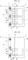
- FIG. 3A is a view of a main part of the voltage determination device A as seen from a side of a first surface 4a of the printed wiring board 4
- FIG. 3B is a view of the main part of the voltage determination device A as seen from a side of a second surface 4b of the printed wiring board 4.
- the printed circuit board 4 is provided with a first substrate terminal 41, a second substrate terminal 42, and a third substrate terminal 43.
- the first to third substrate terminals 41 to 43 are arranged in substantially one line on a first arrangement line L1 which is an imaginary line.
- the first to third substrate terminals 41 to 43 are provided so as to penetrate the printed wiring board 4 from the first surface 4a to the second surface 4b.
- the first to third substrate terminals 41 to 43 are disposed in the vicinity of an end portion 4c on one side of the printed wiring board 4 and are arranged in substantially one line along the end portion 4c.
- the first substrate terminal 41 is a positive power supply terminal connected to the positive terminal of the battery B and the input terminal of the buck-boost converter C.
- the second substrate terminal 42 is a negative power supply terminal connected to the negative terminal of the battery B and the reference potential wiring of the buck-boost converter C.
- the third substrate terminal 43 is a positive power supply terminal connected to the output terminal of the buck-boost converter C.
- the second substrate terminal 42 that is the negative power supply terminal is disposed between the first substrate terminal 41 and the third substrate terminal 43 that are the positive power supply terminals.
- the voltage (first voltage V1P) of the positive terminal of the battery B is input to the first substrate terminal 41 from an outside.
- the voltage of the negative terminal of the battery B and the voltage (second voltage VN) of the negative power supply terminal connected to the reference potential wiring of the buck-boost converter C are input to the second substrate terminal 42 from the outside.
- the voltage (third voltage V2P) of the output terminal of the buck-boost converter C is input to the third substrate terminal 43 from the outside.
- the voltage (first voltage V1P) applied to the first substrate terminal 41 is lower than the voltage (third voltage V2P) applied to the third substrate terminal 43.
- the first voltage determination circuit 1 and the second voltage determination circuit 2 are mounted on the first surface 4a of the printed wiring board 4.
- the first voltage determination circuit 1 and the second voltage determination circuit 2 are disposed on a first side (one side) of the printed wiring board 4 divided by the first arrangement line L1.
- the first voltage determination circuit 1 and the second voltage determination circuit 2 are disposed so that the input terminal 11, the input terminal 12, the input terminal 21, and the input terminal 22 are arranged in substantially one line on a second arrangement line L2 which is an imaginary line. Note that the first arrangement line L1 and the second arrangement line L2 are parallel to each other. In addition, the input terminal 12 and the input terminal 22 are disposed adjacent to each other in a direction along the second arrangement line L2.
- the input terminals 11, 12, 21, and 22 are provided at an end of the first and second voltage determination circuits 1 and 2 on a side close to the first to third substrate terminals 41 to 43.
- the input terminal 11 is disposed at a position close to the first substrate terminal 41.
- the input terminal 12 and the input terminal 22 are disposed at positions close to the second substrate terminal 42.
- the input terminal 21 is disposed at a position close to the third substrate terminal 43.
- a first printed wiring S1, a second printed wiring S2, a third printed wiring S3, and a fourth printed wiring S4 are formed on the first surface 4a of the printed wiring board 4.
- the first to fourth printed wirings S1 to S4 are formed on the printed wiring board 4 in advance.
- the first printed wiring S1 connects the first substrate terminal 41 and the input terminal 11 to each other. Therefore, the input terminal 11 is connected to the positive terminal of the battery B and the input terminal of the buck-boost converter C through the first substrate terminal 41 and the first printed wiring S1.
- the second printed wiring S2 connects the second substrate terminal 42 and the input terminal 12 to each other. Therefore, the input terminal 12 is connected to the negative terminal of the battery B and the reference potential wiring of the buck-boost converter C through the second substrate terminal 42 and the second printed wiring S2.
- the third printed wiring S3 connects the third substrate terminal 43 and the input terminal 21 to each other. Therefore, the input terminal 21 is connected to the output terminal of the buck-boost converter C through the third substrate terminal 43 and the third printed wiring S3.
- the fourth printed wiring S4 connects the second substrate terminal 42 and the input terminal 22 to each other. Therefore, the input terminal 22 is connected to the negative terminal of the battery B and the reference potential wiring of the buck-boost converter C through the second substrate terminal 42 and the fourth printed wiring S4.
- the second substrate terminal 42 to which the input terminals 12 and 22 are connected is common.
- the first to fourth printed wirings S1 to S4 connecting the input terminals 11, 12, 21, and 22 and the first to third substrate terminals 41, 42 and 43, respectively, are provided without intersecting each other and without bypassing a second side (the other side) of the printed wiring board 4 divided by the first arrangement line L1.
- the third voltage determination circuit 3 is mounted on the second surface 4b of the printed wiring board 4.
- the third voltage determination circuit 3 is disposed to face a backside of the second voltage determination circuit 2 with the printed wiring board 4 interposed therebetween.
- the third voltage determination circuit 3 is disposed so that the input terminal 31 faces the input terminal 21 with the printed wiring board 4 interposed therebetween and the input terminal 32 faces the input terminal 22 with the printed wiring board 4 interposed therebetween.
- a fifth printed wiring S5 and a sixth printed wiring S6 are formed on the second surface 4b of the printed wiring board 4.
- the fifth and sixth printed wirings S5 and S6 are formed on the printed wiring board 4 in advance.
- the fifth printed wiring S5 connects the third substrate terminal 43 and the input terminal 31 to each other. Therefore, the input terminal 31 is connected to the output terminal of the buck-boost converter C through the third substrate terminal 43 and the fifth printed wiring S5.
- the sixth printed wiring S6 connects the second substrate terminal 42 and the input terminal 32 to each other. Therefore, the input terminal 32 is connected to the reference potential wiring of the buck-boost converter C through the second substrate terminal 42 and the sixth printed wiring S6.
- the first and second voltage determination circuits 1 and 2 are mounted on the first surface 4a of the printed wiring board 4, the first and second voltage determination circuits 1 and 2 are disposed on the first side (one side) of the printed wiring board 4 divided by the first arrangement line L1, and the second substrate terminal 42 connected to the first and second voltage determination circuits 1 and 2 is common. Therefore, it is possible to dispose the first and second voltage determination circuits 1 and 2 side by side on the first side of the printed wiring board 4 divided by the first arrangement line L1, and it is possible to reduce the number of substrate terminals. Thus, it is possible to limit an increase in a mounting area when the first and second voltage determination circuits 1 and 2 are mounted on the printed wiring board 4.
- the first to fourth printed wirings S1 to S4 are provided without intersecting with each other and without bypassing the second side (the other side) of the printed wiring board 4 divided by the first arrangement line L1 passing through the first to third substrate terminals 41 to 43. Therefore, it is possible to mount the first and second voltage determination circuits 1 and 2 on the printed wiring board 4 in a state in which the insulation performance is secured. That is, according to the present embodiment, it is possible to limit the increase in the mounting area when the first and second voltage determination circuits 1 and 2 are mounted on the printed wiring board 4, and it is possible to secure a predetermined insulation performance.
- first voltage determination circuit 1 and the second voltage determination circuit 2 are disposed so that the input terminal 12 and the input terminal 22 are adjacent to each other. Therefore, it is possible to dispose the second substrate terminal 42 at a position close to both of the input terminals 12 and 22, and therefore it is possible to shorten a distance between the second substrate terminal 42 and the input terminals 12 and 22. Thus, it is possible to more effectively limit the increase in the mounting area when the first and second voltage determination circuits 1 and 2 are mounted on the printed wiring board 4.
- the input terminals 11, 12, 21, and 22 are disposed in substantially one line.
- the first arrangement line L1 passing through the first to third substrate terminals 41 to 43 and the second arrangement line L2 passing through the input terminals 11, 12, 21, and 22 are parallel to each other. Therefore, it is possible to shorten the distance between the first to third substrate terminals 41 to 43 and the input terminals 11, 12, 21, and 22. Thus, it is possible to more effectively limit the increase in the mounting area when the first and second voltage determination circuits 1 and 2 are mounted on the printed wiring board 4.
- the voltage determination device A further includes the third voltage determination circuit 3 that is mounted on the second surface 4b of the printed wiring board 4, is disposed on the first side of the printed wiring board 4 divided by the first arrangement line L1 passing through the first to third substrate terminals 41 to 43, and determines the voltage difference between the second voltage VN and the third voltage V2P. Therefore, since it is possible to mount the third voltage determination circuit 3 for redundancy of the second voltage determination circuit 2 on the printed wiring board 4 so as to face the second voltage determination circuit 2, by using the second surface of the printed wiring board 4, it is possible to limit the increase in the mounting area when the third voltage determination circuit 3 is mounted on the printed wiring board 4.
- the constitution in which the input terminals 11, 12, 21, and 22 are arranged in substantially one line is adopted, but the present invention is not limited thereto.
- the input terminals 11, 12, 21, and 22 may not be arranged in substantially one line as long as the first to fourth printed wirings S1 to S4 are provided without intersecting each other and without bypassing the second side of the printed wiring board 4 divided by the first arrangement line L1 passing through the first to third substrate terminals 41 to 43.
- the third voltage determination circuit 3 may be omitted.
- a fourth voltage determination circuit for redundancy of the first voltage determination circuit 1 may be further provided.
- the fourth voltage determination circuit includes the same constitution as the first voltage determination circuit 1 and determines the input voltage V1 of the battery B.
- the fourth voltage determination circuit includes a fourth high voltage side input terminal connected to the positive terminal of the battery B and the input terminal of the buck-boost converter C, a fourth low voltage side input terminal connected to the negative terminal of the battery B and the reference potential wiring of the buck-boost converter C, and an output terminal connected to the control circuit D.
- the voltage (first voltage V1P) of the positive terminal of the battery B is input to the fourth high voltage side input terminal and the voltage (second voltage VN) of the negative terminal of the battery B is input to the fourth low voltage side input terminal.
- the fourth voltage determination circuit determines the voltage difference between the first voltage V1P and the second voltage VN.
- the output terminal outputs a determination result of the fourth voltage determination circuit to the control circuit D.
- the fourth voltage determination circuit is mounted on the second surface 4b of the printed wiring board 4.
- the fourth voltage determination circuit is disposed to face the backside of the first voltage determination circuit 1 with the printed wiring board 4 interposed therebetween.
- the fourth high voltage side input terminal is disposed to face the input terminal 11 with the printed wiring board 4 interposed therebetween
- the fourth low voltage side input terminal is disposed to face the input terminal 12 with the printed wiring board 4 interposed therebetween. That is, the input terminal 31, the input terminal 32, the fourth high voltage side input terminal, and the fourth low voltage side input terminal are arranged, on the second surface 4b, in substantially one line on the second arrangement line L2.
- the input terminal 32 and the fourth low voltage side input terminal are disposed so as to be adjacent to each other in a direction along the second arrangement line L2.
- a seventh printed wiring that connects the first substrate terminal 41 and the fourth high voltage side input terminal to each other, and an eighth printed wiring that connects the second substrate terminal 42 and the fourth low voltage side input terminal to each other are further formed on the second surface 4b of the printed wiring board 4.
- the second substrate terminal 42 to which the input terminal 32 and the fourth low voltage side input terminal are connected is common.
- the fifth to eighth printed wirings can be provided without intersecting with each other and without bypassing the second side of the printed wiring board 4 divided by the first arrangement line L1.
Landscapes
- Engineering & Computer Science (AREA)
- Microelectronics & Electronic Packaging (AREA)
- Physics & Mathematics (AREA)
- General Physics & Mathematics (AREA)
- Measurement Of Current Or Voltage (AREA)
- Structure Of Printed Boards (AREA)
- Dc-Dc Converters (AREA)
Claims (4)
- Spannungsbestimmungsvorrichtung, umfassend:eine gedruckte Leiterplatte (4), auf der ein erster Substratanschluss (41), dem eine erste Spannung von außen zugeführt wird, ein zweiter Substratanschluss (42), dem eine zweite Spannung von außen zugeführt wird, und ein dritter Substratanschluss (43), dem eine dritte Spannung von außen zugeführt wird, in im Wesentlichen einer Linie angeordnet sind;eine erste Spannungsbestimmungsschaltung (1), die auf einer ersten Oberfläche (4a) der gedruckten Leiterplatte angebracht und dazu ausgelegt ist, eine Spannungsdifferenz zwischen der ersten Spannung und der zweiten Spannung zu bestimmen, wobei die erste Spannungsbestimmungsschaltung auf einer ersten Seite der gedruckten Leiterplatte angeordnet ist, die durch eine erste Anordnungslinie (L1) geteilt ist, die durch den ersten bis dritten Substratanschluss (41-43) verläuft;eine zweite Spannungsbestimmungsschaltung (2), die auf der ersten Oberfläche der gedruckten Leiterplatte angebracht und dazu ausgelegt ist, eine Spannungsdifferenz zwischen der dritten Spannung und der zweiten Spannung zu bestimmen, wobei die zweite Spannungsbestimmungsschaltung auf der ersten Seite der gedruckten Leiterplatte angeordnet ist, die durch die erste Anordnungslinie geteilt ist;gekennzeichnet durcheine erste gedruckte Verdrahtung (S1), die den ersten Substratanschluss (41) und die erste Spannungsbestimmungsschaltung (1) miteinander verbindet;eine zweite gedruckte Verdrahtung (S2), die den zweiten Substratanschluss (42) und die erste Spannungsbestimmungsschaltung (1) miteinander verbindet;eine dritte gedruckte Verdrahtung (S3), die den dritten Substratanschluss (43) und die zweite Spannungsbestimmungsschaltung (2) miteinander verbindet; undeine vierte gedruckte Verdrahtung (S4), die den zweiten Substratanschluss (42) und die zweite Spannungsbestimmungsschaltung (2) miteinander verbindet,wobei die erste bis vierte gedruckte Verdrahtung (S1-S4) bereitgestellt sind, ohne sich gegenseitig zu schneiden und ohne eine zweite Seite der gedruckten Leiterplatte (4) zu umgehen, die durch die erste Anordnungslinie (L1) geteilt ist,wobei die erste Spannungsbestimmungsschaltung (1) einen ersten hochspannungsseitigen Eingangsanschluss (11), der über die erste gedruckte Verdrahtung (S1) mit dem ersten Substratanschluss (41) verbunden ist, undeinen ersten niederspannungsseitigen Eingangsanschluss (12), der über die zweite gedruckte Verdrahtung (S2) mit dem zweiten Substratanschluss (42) verbunden ist, einschließt,die zweite Spannungsbestimmungsschaltung (2) einen zweiten hochspannungsseitigen Eingangsanschluss (21), der über die dritte gedruckte Verdrahtung (S3) mit dem dritten Substratanschluss (43) verbunden ist, und einen zweiten niederspannungsseitigen Eingangsanschluss (22), der über die vierte gedruckte Verdrahtung (S4) mit dem zweiten Substratanschluss (42) verbunden ist, einschließt, unddie erste Spannungsbestimmungsschaltung (1) und die zweite Spannungsbestimmungsschaltung (2) so angeordnet sind, dass der erste niederspannungsseitige Eingangsanschluss (12) und der zweite niederspannungsseitige Eingangsanschluss (22) nebeneinander liegen.
- Spannungsbestimmungsvorrichtung nach Anspruch 1,
wobei der erste hochspannungsseitige Eingangsanschluss, der erste niederspannungsseitige Eingangsanschluss, der zweite niederspannungsseitige Eingangsanschluss und der zweite hochspannungsseitige Eingangsanschluss im Wesentlichen in einer Linie angeordnet sind. - Spannungsbestimmungsvorrichtung nach Anspruch 2,
wobei die erste Anordnungslinie und eine zweite Anordnungslinie (L2), die durch den ersten hochspannungsseitige Eingangsanschluss, den ersten niederspannungsseitige Eingangsanschluss, den zweiten niederspannungsseitigen Eingangsanschluss und den zweiten hochspannungsseitigen Eingangsanschluss verläuft, parallel zueinander sind. - Spannungsbestimmungsvorrichtung nach einem der Ansprüche 1 bis 3, ferner umfassend:eine dritte Spannungsbestimmungsschaltung (3), die auf einer zweiten Oberfläche (4b) angebracht ist, die der ersten Oberfläche der gedruckten Leiterplatte zugewandt ist, und die dazu ausgelegt ist, eine Spannungsdifferenz zwischen der zweiten Spannung und der dritten Spannung zu bestimmen, wobei die dritte Spannungsbestimmungsschaltung auf der ersten Seite der gedruckten Leiterplatte angeordnet ist, die durch die erste Anordnungslinie geteilt ist;eine fünfte gedruckte Verdrahtung (S5), die den dritten Substratanschluss und die dritte Spannungsbestimmungsschaltung miteinander verbindet; undeine sechste gedruckte Verdrahtung (S6), die den zweiten Substratanschluss und die dritte Spannungsbestimmungsschaltung miteinander verbindet.
Applications Claiming Priority (1)
| Application Number | Priority Date | Filing Date | Title |
|---|---|---|---|
| JP2018066818A JP6515425B1 (ja) | 2018-03-30 | 2018-03-30 | 電圧検出装置 |
Publications (2)
| Publication Number | Publication Date |
|---|---|
| EP3565388A1 EP3565388A1 (de) | 2019-11-06 |
| EP3565388B1 true EP3565388B1 (de) | 2021-10-06 |
Family
ID=65812027
Family Applications (1)
| Application Number | Title | Priority Date | Filing Date |
|---|---|---|---|
| EP19161899.0A Active EP3565388B1 (de) | 2018-03-30 | 2019-03-11 | Spannungsbestimmungsvorrichtung |
Country Status (4)
| Country | Link |
|---|---|
| US (1) | US10877078B2 (de) |
| EP (1) | EP3565388B1 (de) |
| JP (1) | JP6515425B1 (de) |
| CN (1) | CN110320399B (de) |
Family Cites Families (13)
| Publication number | Priority date | Publication date | Assignee | Title |
|---|---|---|---|---|
| JP2001174531A (ja) * | 1999-12-15 | 2001-06-29 | Denso Corp | 組電池の異常検出装置 |
| JP4304600B2 (ja) * | 2004-01-19 | 2009-07-29 | 株式会社デンソー | 車両用フライングキャパシタ式電池電圧検出装置 |
| JP4381239B2 (ja) * | 2004-06-25 | 2009-12-09 | 三洋電機株式会社 | 車両用の電源装置 |
| WO2010113455A1 (ja) * | 2009-03-31 | 2010-10-07 | 三洋電機株式会社 | 電池モジュール、バッテリシステムおよび電動車両 |
| JPWO2011024477A1 (ja) * | 2009-08-31 | 2013-01-24 | 三洋電機株式会社 | バッテリモジュール、バッテリシステムおよび電動車両 |
| CN201666911U (zh) * | 2010-02-23 | 2010-12-08 | 深圳市英威腾电气股份有限公司 | 中高压变频调速器电压检测装置 |
| JP6107406B2 (ja) * | 2013-05-20 | 2017-04-05 | 株式会社デンソー | 電池監視装置 |
| JP6046103B2 (ja) * | 2014-10-03 | 2016-12-14 | 財團法人工業技術研究院Industrial Technology Research Institute | 圧力アレイセンサモジュールおよびその製造方法 |
| JP6541223B2 (ja) | 2015-01-16 | 2019-07-10 | 新日本無線株式会社 | 半導体装置 |
| JP6298015B2 (ja) * | 2015-07-08 | 2018-03-20 | ファナック株式会社 | 劣化検出機能を備えたプリント基板及びそれを具備するモータ駆動装置 |
| JP2017049199A (ja) * | 2015-09-04 | 2017-03-09 | トヨタ自動車株式会社 | 電圧監視装置 |
| US20170222282A1 (en) * | 2016-02-01 | 2017-08-03 | Lear Corporation | Battery diagnostic sensor unit |
| JP2017167050A (ja) * | 2016-03-17 | 2017-09-21 | 株式会社ケーヒン | 電圧検出装置 |
-
2018
- 2018-03-30 JP JP2018066818A patent/JP6515425B1/ja active Active
-
2019
- 2019-03-11 EP EP19161899.0A patent/EP3565388B1/de active Active
- 2019-03-14 US US16/353,264 patent/US10877078B2/en active Active
- 2019-03-27 CN CN201910236656.6A patent/CN110320399B/zh active Active
Also Published As
| Publication number | Publication date |
|---|---|
| EP3565388A1 (de) | 2019-11-06 |
| JP6515425B1 (ja) | 2019-05-22 |
| CN110320399A (zh) | 2019-10-11 |
| US10877078B2 (en) | 2020-12-29 |
| CN110320399B (zh) | 2023-08-04 |
| JP2019178885A (ja) | 2019-10-17 |
| US20190302153A1 (en) | 2019-10-03 |
Similar Documents
| Publication | Publication Date | Title |
|---|---|---|
| US10586970B2 (en) | Wiring module | |
| EP1881592B1 (de) | Stromwandler | |
| US8760847B2 (en) | Low inductance capacitor assembly | |
| WO2007138645A1 (ja) | 車両用補助電源装置 | |
| US11011996B2 (en) | Power converter | |
| US10424947B2 (en) | Battery monitoring device | |
| EP2604477A1 (de) | Steuervorrichtung | |
| EP2517243B1 (de) | Hybridschaltung | |
| EP3565388B1 (de) | Spannungsbestimmungsvorrichtung | |
| US10326442B2 (en) | Assembly having internally configurable solid-state switch arrangement for use as one or more disconnection switches in electrical systems and having external package common to the electrical systems | |
| CN106663676A (zh) | 半导体装置以及多相用半导体装置 | |
| JP2011194958A (ja) | 電子制御装置 | |
| US20240186272A1 (en) | Power module | |
| JP5118520B2 (ja) | 信号処理モジュール | |
| JP7435402B2 (ja) | フレキシブル基板 | |
| US11431178B2 (en) | Battery system | |
| US10547292B2 (en) | Electric circuit device | |
| JP2013021748A (ja) | インテリジェント・モジュール | |
| US20120326507A1 (en) | Power conversion apparatus having casing accommodated with a plurality of circuit boards | |
| US11081814B2 (en) | Wiring module | |
| US10637216B2 (en) | Power control system with improved thermal performance | |
| CN1947329B (zh) | 一种用于汽车发电机单元的整体调节器的制造方法 | |
| US20040056534A1 (en) | Planar DC-DC converter for multi-volt electrical applications | |
| JP6873368B2 (ja) | 電力変換装置 | |
| JP2020071929A (ja) | 電池監視装置 |
Legal Events
| Date | Code | Title | Description |
|---|---|---|---|
| PUAI | Public reference made under article 153(3) epc to a published international application that has entered the european phase |
Free format text: ORIGINAL CODE: 0009012 |
|
| STAA | Information on the status of an ep patent application or granted ep patent |
Free format text: STATUS: THE APPLICATION HAS BEEN PUBLISHED |
|
| AK | Designated contracting states |
Kind code of ref document: A1 Designated state(s): AL AT BE BG CH CY CZ DE DK EE ES FI FR GB GR HR HU IE IS IT LI LT LU LV MC MK MT NL NO PL PT RO RS SE SI SK SM TR |
|
| AX | Request for extension of the european patent |
Extension state: BA ME |
|
| STAA | Information on the status of an ep patent application or granted ep patent |
Free format text: STATUS: REQUEST FOR EXAMINATION WAS MADE |
|
| 17P | Request for examination filed |
Effective date: 20200504 |
|
| RBV | Designated contracting states (corrected) |
Designated state(s): AL AT BE BG CH CY CZ DE DK EE ES FI FR GB GR HR HU IE IS IT LI LT LU LV MC MK MT NL NO PL PT RO RS SE SI SK SM TR |
|
| GRAP | Despatch of communication of intention to grant a patent |
Free format text: ORIGINAL CODE: EPIDOSNIGR1 |
|
| STAA | Information on the status of an ep patent application or granted ep patent |
Free format text: STATUS: GRANT OF PATENT IS INTENDED |
|
| INTG | Intention to grant announced |
Effective date: 20210607 |
|
| RAP1 | Party data changed (applicant data changed or rights of an application transferred) |
Owner name: HITACHI ASTEMO, LTD. |
|
| GRAS | Grant fee paid |
Free format text: ORIGINAL CODE: EPIDOSNIGR3 |
|
| GRAA | (expected) grant |
Free format text: ORIGINAL CODE: 0009210 |
|
| STAA | Information on the status of an ep patent application or granted ep patent |
Free format text: STATUS: THE PATENT HAS BEEN GRANTED |
|
| AK | Designated contracting states |
Kind code of ref document: B1 Designated state(s): AL AT BE BG CH CY CZ DE DK EE ES FI FR GB GR HR HU IE IS IT LI LT LU LV MC MK MT NL NO PL PT RO RS SE SI SK SM TR |
|
| REG | Reference to a national code |
Ref country code: GB Ref legal event code: FG4D |
|
| REG | Reference to a national code |
Ref country code: CH Ref legal event code: EP Ref country code: AT Ref legal event code: REF Ref document number: 1437420 Country of ref document: AT Kind code of ref document: T Effective date: 20211015 |
|
| REG | Reference to a national code |
Ref country code: DE Ref legal event code: R096 Ref document number: 602019008071 Country of ref document: DE |
|
| REG | Reference to a national code |
Ref country code: IE Ref legal event code: FG4D |
|
| REG | Reference to a national code |
Ref country code: LT Ref legal event code: MG9D |
|
| REG | Reference to a national code |
Ref country code: NL Ref legal event code: MP Effective date: 20211006 |
|
| REG | Reference to a national code |
Ref country code: AT Ref legal event code: MK05 Ref document number: 1437420 Country of ref document: AT Kind code of ref document: T Effective date: 20211006 |
|
| PG25 | Lapsed in a contracting state [announced via postgrant information from national office to epo] |
Ref country code: RS Free format text: LAPSE BECAUSE OF FAILURE TO SUBMIT A TRANSLATION OF THE DESCRIPTION OR TO PAY THE FEE WITHIN THE PRESCRIBED TIME-LIMIT Effective date: 20211006 Ref country code: LT Free format text: LAPSE BECAUSE OF FAILURE TO SUBMIT A TRANSLATION OF THE DESCRIPTION OR TO PAY THE FEE WITHIN THE PRESCRIBED TIME-LIMIT Effective date: 20211006 Ref country code: FI Free format text: LAPSE BECAUSE OF FAILURE TO SUBMIT A TRANSLATION OF THE DESCRIPTION OR TO PAY THE FEE WITHIN THE PRESCRIBED TIME-LIMIT Effective date: 20211006 Ref country code: BG Free format text: LAPSE BECAUSE OF FAILURE TO SUBMIT A TRANSLATION OF THE DESCRIPTION OR TO PAY THE FEE WITHIN THE PRESCRIBED TIME-LIMIT Effective date: 20220106 Ref country code: AT Free format text: LAPSE BECAUSE OF FAILURE TO SUBMIT A TRANSLATION OF THE DESCRIPTION OR TO PAY THE FEE WITHIN THE PRESCRIBED TIME-LIMIT Effective date: 20211006 |
|
| PG25 | Lapsed in a contracting state [announced via postgrant information from national office to epo] |
Ref country code: IS Free format text: LAPSE BECAUSE OF FAILURE TO SUBMIT A TRANSLATION OF THE DESCRIPTION OR TO PAY THE FEE WITHIN THE PRESCRIBED TIME-LIMIT Effective date: 20220206 Ref country code: SE Free format text: LAPSE BECAUSE OF FAILURE TO SUBMIT A TRANSLATION OF THE DESCRIPTION OR TO PAY THE FEE WITHIN THE PRESCRIBED TIME-LIMIT Effective date: 20211006 Ref country code: PT Free format text: LAPSE BECAUSE OF FAILURE TO SUBMIT A TRANSLATION OF THE DESCRIPTION OR TO PAY THE FEE WITHIN THE PRESCRIBED TIME-LIMIT Effective date: 20220207 Ref country code: PL Free format text: LAPSE BECAUSE OF FAILURE TO SUBMIT A TRANSLATION OF THE DESCRIPTION OR TO PAY THE FEE WITHIN THE PRESCRIBED TIME-LIMIT Effective date: 20211006 Ref country code: NO Free format text: LAPSE BECAUSE OF FAILURE TO SUBMIT A TRANSLATION OF THE DESCRIPTION OR TO PAY THE FEE WITHIN THE PRESCRIBED TIME-LIMIT Effective date: 20220106 Ref country code: NL Free format text: LAPSE BECAUSE OF FAILURE TO SUBMIT A TRANSLATION OF THE DESCRIPTION OR TO PAY THE FEE WITHIN THE PRESCRIBED TIME-LIMIT Effective date: 20211006 Ref country code: LV Free format text: LAPSE BECAUSE OF FAILURE TO SUBMIT A TRANSLATION OF THE DESCRIPTION OR TO PAY THE FEE WITHIN THE PRESCRIBED TIME-LIMIT Effective date: 20211006 Ref country code: HR Free format text: LAPSE BECAUSE OF FAILURE TO SUBMIT A TRANSLATION OF THE DESCRIPTION OR TO PAY THE FEE WITHIN THE PRESCRIBED TIME-LIMIT Effective date: 20211006 Ref country code: GR Free format text: LAPSE BECAUSE OF FAILURE TO SUBMIT A TRANSLATION OF THE DESCRIPTION OR TO PAY THE FEE WITHIN THE PRESCRIBED TIME-LIMIT Effective date: 20220107 Ref country code: ES Free format text: LAPSE BECAUSE OF FAILURE TO SUBMIT A TRANSLATION OF THE DESCRIPTION OR TO PAY THE FEE WITHIN THE PRESCRIBED TIME-LIMIT Effective date: 20211006 |
|
| REG | Reference to a national code |
Ref country code: DE Ref legal event code: R097 Ref document number: 602019008071 Country of ref document: DE |
|
| PG25 | Lapsed in a contracting state [announced via postgrant information from national office to epo] |
Ref country code: SM Free format text: LAPSE BECAUSE OF FAILURE TO SUBMIT A TRANSLATION OF THE DESCRIPTION OR TO PAY THE FEE WITHIN THE PRESCRIBED TIME-LIMIT Effective date: 20211006 Ref country code: SK Free format text: LAPSE BECAUSE OF FAILURE TO SUBMIT A TRANSLATION OF THE DESCRIPTION OR TO PAY THE FEE WITHIN THE PRESCRIBED TIME-LIMIT Effective date: 20211006 Ref country code: RO Free format text: LAPSE BECAUSE OF FAILURE TO SUBMIT A TRANSLATION OF THE DESCRIPTION OR TO PAY THE FEE WITHIN THE PRESCRIBED TIME-LIMIT Effective date: 20211006 Ref country code: EE Free format text: LAPSE BECAUSE OF FAILURE TO SUBMIT A TRANSLATION OF THE DESCRIPTION OR TO PAY THE FEE WITHIN THE PRESCRIBED TIME-LIMIT Effective date: 20211006 Ref country code: DK Free format text: LAPSE BECAUSE OF FAILURE TO SUBMIT A TRANSLATION OF THE DESCRIPTION OR TO PAY THE FEE WITHIN THE PRESCRIBED TIME-LIMIT Effective date: 20211006 Ref country code: CZ Free format text: LAPSE BECAUSE OF FAILURE TO SUBMIT A TRANSLATION OF THE DESCRIPTION OR TO PAY THE FEE WITHIN THE PRESCRIBED TIME-LIMIT Effective date: 20211006 |
|
| PLBE | No opposition filed within time limit |
Free format text: ORIGINAL CODE: 0009261 |
|
| STAA | Information on the status of an ep patent application or granted ep patent |
Free format text: STATUS: NO OPPOSITION FILED WITHIN TIME LIMIT |
|
| 26N | No opposition filed |
Effective date: 20220707 |
|
| PG25 | Lapsed in a contracting state [announced via postgrant information from national office to epo] |
Ref country code: MC Free format text: LAPSE BECAUSE OF FAILURE TO SUBMIT A TRANSLATION OF THE DESCRIPTION OR TO PAY THE FEE WITHIN THE PRESCRIBED TIME-LIMIT Effective date: 20211006 Ref country code: AL Free format text: LAPSE BECAUSE OF FAILURE TO SUBMIT A TRANSLATION OF THE DESCRIPTION OR TO PAY THE FEE WITHIN THE PRESCRIBED TIME-LIMIT Effective date: 20211006 |
|
| REG | Reference to a national code |
Ref country code: CH Ref legal event code: PL |
|
| PG25 | Lapsed in a contracting state [announced via postgrant information from national office to epo] |
Ref country code: SI Free format text: LAPSE BECAUSE OF FAILURE TO SUBMIT A TRANSLATION OF THE DESCRIPTION OR TO PAY THE FEE WITHIN THE PRESCRIBED TIME-LIMIT Effective date: 20211006 |
|
| REG | Reference to a national code |
Ref country code: BE Ref legal event code: MM Effective date: 20220331 |
|
| PG25 | Lapsed in a contracting state [announced via postgrant information from national office to epo] |
Ref country code: LU Free format text: LAPSE BECAUSE OF NON-PAYMENT OF DUE FEES Effective date: 20220311 Ref country code: LI Free format text: LAPSE BECAUSE OF NON-PAYMENT OF DUE FEES Effective date: 20220331 Ref country code: IE Free format text: LAPSE BECAUSE OF NON-PAYMENT OF DUE FEES Effective date: 20220311 Ref country code: CH Free format text: LAPSE BECAUSE OF NON-PAYMENT OF DUE FEES Effective date: 20220331 |
|
| PG25 | Lapsed in a contracting state [announced via postgrant information from national office to epo] |
Ref country code: BE Free format text: LAPSE BECAUSE OF NON-PAYMENT OF DUE FEES Effective date: 20220331 |
|
| PG25 | Lapsed in a contracting state [announced via postgrant information from national office to epo] |
Ref country code: IT Free format text: LAPSE BECAUSE OF FAILURE TO SUBMIT A TRANSLATION OF THE DESCRIPTION OR TO PAY THE FEE WITHIN THE PRESCRIBED TIME-LIMIT Effective date: 20211006 |
|
| GBPC | Gb: european patent ceased through non-payment of renewal fee |
Effective date: 20230311 |
|
| PG25 | Lapsed in a contracting state [announced via postgrant information from national office to epo] |
Ref country code: GB Free format text: LAPSE BECAUSE OF NON-PAYMENT OF DUE FEES Effective date: 20230311 |
|
| PG25 | Lapsed in a contracting state [announced via postgrant information from national office to epo] |
Ref country code: GB Free format text: LAPSE BECAUSE OF NON-PAYMENT OF DUE FEES Effective date: 20230311 |
|
| PG25 | Lapsed in a contracting state [announced via postgrant information from national office to epo] |
Ref country code: MK Free format text: LAPSE BECAUSE OF FAILURE TO SUBMIT A TRANSLATION OF THE DESCRIPTION OR TO PAY THE FEE WITHIN THE PRESCRIBED TIME-LIMIT Effective date: 20211006 Ref country code: CY Free format text: LAPSE BECAUSE OF FAILURE TO SUBMIT A TRANSLATION OF THE DESCRIPTION OR TO PAY THE FEE WITHIN THE PRESCRIBED TIME-LIMIT Effective date: 20211006 |
|
| PG25 | Lapsed in a contracting state [announced via postgrant information from national office to epo] |
Ref country code: HU Free format text: LAPSE BECAUSE OF FAILURE TO SUBMIT A TRANSLATION OF THE DESCRIPTION OR TO PAY THE FEE WITHIN THE PRESCRIBED TIME-LIMIT; INVALID AB INITIO Effective date: 20190311 |
|
| PG25 | Lapsed in a contracting state [announced via postgrant information from national office to epo] |
Ref country code: MT Free format text: LAPSE BECAUSE OF FAILURE TO SUBMIT A TRANSLATION OF THE DESCRIPTION OR TO PAY THE FEE WITHIN THE PRESCRIBED TIME-LIMIT Effective date: 20211006 |
|
| PG25 | Lapsed in a contracting state [announced via postgrant information from national office to epo] |
Ref country code: TR Free format text: LAPSE BECAUSE OF FAILURE TO SUBMIT A TRANSLATION OF THE DESCRIPTION OR TO PAY THE FEE WITHIN THE PRESCRIBED TIME-LIMIT Effective date: 20211006 |
|
| PGFP | Annual fee paid to national office [announced via postgrant information from national office to epo] |
Ref country code: DE Payment date: 20260128 Year of fee payment: 8 |
|
| PGFP | Annual fee paid to national office [announced via postgrant information from national office to epo] |
Ref country code: FR Payment date: 20260209 Year of fee payment: 8 |