EP3565055A1 - In line e-probe waveguide transition - Google Patents
In line e-probe waveguide transition Download PDFInfo
- Publication number
- EP3565055A1 EP3565055A1 EP19169997.4A EP19169997A EP3565055A1 EP 3565055 A1 EP3565055 A1 EP 3565055A1 EP 19169997 A EP19169997 A EP 19169997A EP 3565055 A1 EP3565055 A1 EP 3565055A1
- Authority
- EP
- European Patent Office
- Prior art keywords
- wall
- channel
- transition device
- longitudinal axis
- waveguide
- Prior art date
- Legal status (The legal status is an assumption and is not a legal conclusion. Google has not performed a legal analysis and makes no representation as to the accuracy of the status listed.)
- Granted
Links
Images


Classifications
-
- H—ELECTRICITY
- H01—ELECTRIC ELEMENTS
- H01P—WAVEGUIDES; RESONATORS, LINES, OR OTHER DEVICES OF THE WAVEGUIDE TYPE
- H01P5/00—Coupling devices of the waveguide type
- H01P5/08—Coupling devices of the waveguide type for linking dissimilar lines or devices
- H01P5/10—Coupling devices of the waveguide type for linking dissimilar lines or devices for coupling balanced lines or devices with unbalanced lines or devices
- H01P5/103—Hollow-waveguide/coaxial-line transitions
-
- H—ELECTRICITY
- H01—ELECTRIC ELEMENTS
- H01P—WAVEGUIDES; RESONATORS, LINES, OR OTHER DEVICES OF THE WAVEGUIDE TYPE
- H01P5/00—Coupling devices of the waveguide type
- H01P5/02—Coupling devices of the waveguide type with invariable factor of coupling
- H01P5/022—Transitions between lines of the same kind and shape, but with different dimensions
- H01P5/024—Transitions between lines of the same kind and shape, but with different dimensions between hollow waveguides
-
- H—ELECTRICITY
- H01—ELECTRIC ELEMENTS
- H01P—WAVEGUIDES; RESONATORS, LINES, OR OTHER DEVICES OF THE WAVEGUIDE TYPE
- H01P1/00—Auxiliary devices
- H01P1/04—Fixed joints
- H01P1/042—Hollow waveguide joints
-
- H—ELECTRICITY
- H01—ELECTRIC ELEMENTS
- H01P—WAVEGUIDES; RESONATORS, LINES, OR OTHER DEVICES OF THE WAVEGUIDE TYPE
- H01P3/00—Waveguides; Transmission lines of the waveguide type
- H01P3/12—Hollow waveguides
-
- H—ELECTRICITY
- H05—ELECTRIC TECHNIQUES NOT OTHERWISE PROVIDED FOR
- H05B—ELECTRIC HEATING; ELECTRIC LIGHT SOURCES NOT OTHERWISE PROVIDED FOR; CIRCUIT ARRANGEMENTS FOR ELECTRIC LIGHT SOURCES, IN GENERAL
- H05B6/00—Heating by electric, magnetic or electromagnetic fields
- H05B6/64—Heating using microwaves
- H05B6/66—Circuits
- H05B6/68—Circuits for monitoring or control
- H05B6/687—Circuits for monitoring or control for cooking
-
- H—ELECTRICITY
- H05—ELECTRIC TECHNIQUES NOT OTHERWISE PROVIDED FOR
- H05B—ELECTRIC HEATING; ELECTRIC LIGHT SOURCES NOT OTHERWISE PROVIDED FOR; CIRCUIT ARRANGEMENTS FOR ELECTRIC LIGHT SOURCES, IN GENERAL
- H05B6/00—Heating by electric, magnetic or electromagnetic fields
- H05B6/64—Heating using microwaves
- H05B6/70—Feed lines
- H05B6/705—Feed lines using microwave tuning
-
- H—ELECTRICITY
- H05—ELECTRIC TECHNIQUES NOT OTHERWISE PROVIDED FOR
- H05B—ELECTRIC HEATING; ELECTRIC LIGHT SOURCES NOT OTHERWISE PROVIDED FOR; CIRCUIT ARRANGEMENTS FOR ELECTRIC LIGHT SOURCES, IN GENERAL
- H05B6/00—Heating by electric, magnetic or electromagnetic fields
- H05B6/64—Heating using microwaves
- H05B6/70—Feed lines
- H05B6/707—Feed lines using waveguides
-
- H—ELECTRICITY
- H05—ELECTRIC TECHNIQUES NOT OTHERWISE PROVIDED FOR
- H05B—ELECTRIC HEATING; ELECTRIC LIGHT SOURCES NOT OTHERWISE PROVIDED FOR; CIRCUIT ARRANGEMENTS FOR ELECTRIC LIGHT SOURCES, IN GENERAL
- H05B6/00—Heating by electric, magnetic or electromagnetic fields
- H05B6/64—Heating using microwaves
- H05B6/72—Radiators or antennas
Definitions
- the present device generally relates to a waveguide for electromagnetic field propagation, and, more specifically, to a longitudinal transition for a waveguide.
- Microwave transmitters are commonly connected to cavities of microwave ovens via transmission lines. Such transmission lines may be coupled to cooking cavities of microwaves via waveguides.
- the disclosure provides for a novel transition for a longitudinal waveguide as described in the following detailed description.
- a transition device for a hollow waveguide comprises a rectangular structure comprising an inlet wall and interior extending from the inlet wall along a longitudinal axis.
- the inlet wall is configured to receive a transmission line comprising an antenna.
- the antenna forms a proximal end proximate to the inlet wall and a distal end configured to extend into the rectangular structure of the hollow waveguide.
- a channel is formed in the rectangular structure.
- the channel comprises a base forming a tuning surface.
- the tuning surface is configured to extend along a length of the antenna in a spaced configuration parallel to the longitudinal axis.
- a method for generating an electrical field in a hollow waveguide comprises transmitting electrical current at a frequency into an inlet wall of the hollow waveguide via a transmission line.
- the method further comprises emitting electromagnetic energy radially from an antenna at the frequency perpendicular to a longitudinal axis of the hollow waveguide.
- the method further comprises tuning the electromagnetic energy via an excitation surface of a channel that at least partially bisects the hollow waveguide.
- the method additionally comprises controlling the electromagnetic energy via the channel in a cavity extending between the inlet wall and the channel. The electromagnetic energy is controlled to propagate parallel to the longitudinal axis of the hollow waveguide.
- a transition device for a hollow waveguide is disclosed.
- the transition device comprises an elongated rectangular structure comprising an inlet wall and an interior volume extending from the inlet wall along a longitudinal axis.
- the inlet wall is configured to receive a transmission line comprising an antenna forming a proximal end proximate to the inlet wall and a distal end configured to extend into the rectangular structure.
- a capacitive channel is formed through a width of the rectangular structure substantially perpendicular to the longitudinal axis.
- the capacitive channel comprises a base portion forming a tuning surface.
- the tuning surface is configured to extend along a length of the antenna in a space configuration parallel to the longitudinal axis of the elongated rectangular structure.
- the terms "upper,” “lower,” “right,” “left,” “rear,” “front,” “vertical,” “horizontal,” and derivatives thereof shall relate to the device as oriented in FIG. 1 .
- the device may assume various alternative orientations and step sequences, except where expressly specified to the contrary.
- the specific devices and processes illustrated in the attached drawings, and described in the following specification are simply exemplary embodiments of the inventive concepts defined in the appended claims. Hence, specific dimensions and other physical characteristics relating to the embodiments disclosed herein are not to be considered as limiting, unless the claims expressly state otherwise.
- the transition device 10 may be configured to receive a transmission line 14 via an inlet wall 16.
- the waveguide 12 may generally form an elongated rectangular form having a Height and a Width extending along a longitudinal axis L.
- the longitudinal transition device 10 may provide for an inline transition for the transmission line 14 configured to generate transverse electric propagation of electromagnetic radiation transmitted through the waveguide 12 along the longitudinal axis L.
- a rectangular channel 18 may be formed through the width W of the hollow waveguide 12.
- the rectangular channel 18 may form a cavity 20 extending from the inlet wall 16 to a first wall 22 of the rectangular channel 18.
- a base portion 24 may extend from the first wall 22 of the rectangular channel 18 to a second wall 26 of the rectangular channel 18.
- the rectangular channel 18 may at least partially bisect an interior volume 28 of the hollow waveguide 12 providing for the cavity 20 to be formed proximate to the inlet wall 16. Accordingly, the first wall 22 and the opening formed by the channel 18 may define a length of the cavity 20.
- the transition device 10 of the waveguide 12 may be configured to receive a probe 30 or antenna extending through the inlet wall 16 from the transmission line 14.
- the probe 30 may extend along the longitudinal axis L of the waveguide 12 from a proximal end portion 30a at the inlet wall 16 to a distal end portion 30b.
- the distal end portion 30b may terminate proximate to the second wall 26 of the rectangular channel 18.
- the probe 30 may extend parallel to a tuning surface 32 within the interior volume 28 formed by the base portion 24 of the rectangular channel 18.
- the rectangular channel 18 may form a cutout portion extending transverse to the longitudinal axis L of the waveguide 12 and provide a capacitive tuning channel (e.g. the rectangular channel 18) via the tuning surface 32.
- the transmission line 14 may correspond to a coaxial transmission line or other forms of conductive connectors.
- the probe 30 may correspond to a core portion of the transmission line 14, and, in some embodiments, may be implemented to an antenna or a microstrip antenna.
- the operation of the transition device 10 may be derived based on the duality theorem of quantum mechanics such that the transition device 10 is optimized to propagate electromagnetic radiation through the hollow waveguide 12 at a desired frequency. In some embodiments, the desired frequency may be between approximately 2.4 and 2.5 GHz. As further discussed in reference to FIGS. 4 and 5 , the performance of the transition device 10 may be optimized to transmit power from the inlet wall 16 to an outlet 34 depicted in FIG. 1 as a rectangular aperture formed in an exterior wall 36 of the waveguide 12.
- the waveguide 12 may comprise rectangular transition portion 38 formed perpendicular to the waveguide 12.
- the transition section 38 may perpendicularly or angularly align with a passage formed by the interior volume 28 of the waveguide 12.
- the transition section 38 may be configured to transmit the electromagnetic radiation upward from a linear portion of the waveguide 12 extending along the longitudinal axis to the outlet 34 formed in the exterior wall 36.
- the waveguide 12 may be configured to transmit the electromagnetic radiation through the interior volume 28 outward through the outlet 34.
- FIG. 2 demonstrates a detailed projected view of the transition device 10 of the waveguide 12 in accordance with the disclosure.
- the distal end portion 30b of the probe 30 is shown extending from the proximal end portion 30a parallel to the tuning surface 32 formed by the base portion 24 of the rectangular channel 18.
- the distal end portion 30b may terminate proximate to the second wall 26 of the rectangular channel 18. In this configuration, electromagnetic radiation may be emitted radially outward from the probe 30 and substantially into the tuning surface 32 of the rectangular channel 18.
- the electromagnetic radiation emitted from the probe 30 may be controlled by the transition device 10 to propagate perpendicular to the longitudinal axis L of the waveguide 12 outward toward the outlet 34.
- the transition device 10 may provide for the electromagnetic radiation emitted from the probe 30 to be transmitted through the hollow waveguide 12 at a high level of efficiency. The propagation of the waves through the waveguide 12 is further discussed in reference to FIGS. 4 and 5 .
- the proportions of the rectangular channel 18 and the cavity 20 may provide for the efficient control and transmission of wavelengths through the waveguide 12 at a target frequency or frequency range.
- the specific proportions of an exemplary embodiment of the transition device 10 are demonstrated. Though the specific dimensional values for the proportions of the transition device 10 are discussed in reference to FIG. 3 , the dimensions of the device may vary based on a desired frequency transmission range, proportions of the waveguide device, or various additional factors that may be understood to those having skill in the art. Accordingly, the invention as discussed herein may not be limited by the specific dimensional specifications provided here, which are provided to clearly describe at least one exemplary embodiment.
- the transition device 10 may be configured having specific dimensional proportions.
- the transmission line 14 may comprise a transmission line diameter 40 configured to engage the inlet wall 16 at an engagement height 42.
- the cavity 20 may extend a cavity height 46 from a lower surface 44 of the transition device 10.
- the cavity 20 may extend above the transmission line 14 and the probe 30 creating a volumetric opening in contiguous connection with the interior volume 28 formed by the rectangular structure of the hollow waveguide 12.
- the cavity 20 may further extend forward from the inlet wall 16 to the first wall 22 along a cavity length 48. Accordingly, the cavity 20 may be formed above the probe 30 extending along the longitudinal axis L of the hollow waveguide 12 from the inlet wall 16 to the first wall 22 of the rectangular channel 18.
- the rectangular channel 18 may comprise a channel height 50 formed by the first wall 22 and the second wall 26.
- the base portion 24 may separate the first wall 22 from the second wall 26 by a base length 52.
- a tuning surface 32 formed by the base portion 24 of the rectangular channel 18 may extend in a spaced configuration parallel to the probe 30.
- the probe 30 may comprise the distal end portion 30b extending from the proximal end portion 30a along a probe length 54. In this configuration, a probe diameter 56 or thickness of the probe 30 may terminate at the distal end portion 30b proximate to the second wall 26 of the rectangular channel 18.
- the base length 52 of the rectangular channel 18 may be greater than the cavity length 48 of the cavity 20.
- the channel height 50 may extend from an upper surface 58 to the base portion 24 such that the probe 30 is at least partially separated from the tuning surface 32 in a spaced configuration.
- the probe length 54 may be configured to extend such that the distal end portion 30b extends along the longitudinal axis L of the waveguide 12 from the inlet wall 16 to beyond the second wall 26 of the rectangular channel 18.
- longitudinal transition device 10 may be interpreted from the exemplary dimensions provided in Table 1.
- Table 1 Exemplary dimensions for longitudinal transition device Element No. Element Description Dimension (mm) 40 transmission line diameter 9.0 42 engagement height 5.8 46 cavity height 28.0 48 cavity length 11.0 50 channel height 19.0 52 base length 12.0 54 probe length 24.5 56 probe diameter 3.0
- the transition device 10 is shown having an input signal with a target frequency simulated as an input to the transmission line 14.
- the target frequency of the input signal applied to the transmission line 14 may be approximately 2.4 GHz to 2.5 GHz.
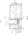
- a plurality of magnetic field lines 62 are demonstrated as directional arrows indicating the direction of the electromagnetic field induced within the transition device 10 of the hollow waveguide 12.
- the magnetic field lines 62 radiate outward from the probe 30 into the interior volume 28 formed by the transition device 10. In the cavity 20, the magnetic field lines 62 flow approximately from the first wall 22 to the inlet wall 16.
- the magnetic field lines 62 flow outward from the second wall 26 toward the outlet 34 of the waveguide 12. Based on the configuration of the rectangular channel 18 and the cavity 20, the magnetic field lines 62 in a body portion of the waveguide 12 propagate perpendicular to the longitudinal axis L of the hollow waveguide 12. In this way, the longitudinal transition device 10 discussed herein provides for the control of the electromagnetic field within the hollow waveguide 12 such that the magnetic field lines 62 are propagated perpendicular to the longitudinal axis L as the electromagnetic energy is transmitted through the hollow waveguide 12.
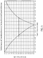
- FIG. 5 a plot of the power reflected back within the waveguide 12 to the inlet wall 16 is shown.
- the amount of power or electromagnetic energy reflected back to the inlet wall 16 is demonstrated at the target wavelengths ranging from 2.4 GHz to 2.5 GHz.
- the amount of power reflected back to the inlet wall 16 may be an indication of negative performance characteristics that may limit the transmission of the electromagnetic energy from the waveguide 12 into a microwave heating cavity.
- the energy reflected back by the waveguide 12 to the inlet wall 16 is less than one percent (1%) of the total power delivered into the waveguide 12.
- the longitudinal transition device 10 of the hollow waveguide 12 may provide for efficient operation and transmission of the electromagnetic energy into a microwave cavity.
- the term "coupled” in all of its forms, couple, coupling, coupled, etc. generally means the joining of two components (electrical or mechanical) directly or indirectly to one another. Such joining may be stationary in nature or movable in nature. Such joining may be achieved with the two components (electrical or mechanical) and any additional intermediate members being integrally formed as a single unitary body with one another or with the two components. Such joining may be permanent in nature or may be removable or releasable in nature unless otherwise stated.
Landscapes
- Physics & Mathematics (AREA)
- Electromagnetism (AREA)
- Control Of Motors That Do Not Use Commutators (AREA)
- Waveguide Aerials (AREA)
Abstract
Description
- The present device generally relates to a waveguide for electromagnetic field propagation, and, more specifically, to a longitudinal transition for a waveguide.
- Microwave transmitters are commonly connected to cavities of microwave ovens via transmission lines. Such transmission lines may be coupled to cooking cavities of microwaves via waveguides. The disclosure provides for a novel transition for a longitudinal waveguide as described in the following detailed description.
- In at least one aspect, a transition device for a hollow waveguide is disclosed. The device comprises a rectangular structure comprising an inlet wall and interior extending from the inlet wall along a longitudinal axis. The inlet wall is configured to receive a transmission line comprising an antenna. The antenna forms a proximal end proximate to the inlet wall and a distal end configured to extend into the rectangular structure of the hollow waveguide. A channel is formed in the rectangular structure. The channel comprises a base forming a tuning surface. The tuning surface is configured to extend along a length of the antenna in a spaced configuration parallel to the longitudinal axis.
- In at least another aspect, a method for generating an electrical field in a hollow waveguide is disclosed. The method comprises transmitting electrical current at a frequency into an inlet wall of the hollow waveguide via a transmission line. The method further comprises emitting electromagnetic energy radially from an antenna at the frequency perpendicular to a longitudinal axis of the hollow waveguide. The method further comprises tuning the electromagnetic energy via an excitation surface of a channel that at least partially bisects the hollow waveguide. The method additionally comprises controlling the electromagnetic energy via the channel in a cavity extending between the inlet wall and the channel. The electromagnetic energy is controlled to propagate parallel to the longitudinal axis of the hollow waveguide. In at least another aspect, a transition device for a hollow waveguide is disclosed. The transition device comprises an elongated rectangular structure comprising an inlet wall and an interior volume extending from the inlet wall along a longitudinal axis. The inlet wall is configured to receive a transmission line comprising an antenna forming a proximal end proximate to the inlet wall and a distal end configured to extend into the rectangular structure. A capacitive channel is formed through a width of the rectangular structure substantially perpendicular to the longitudinal axis. The capacitive channel comprises a base portion forming a tuning surface. The tuning surface is configured to extend along a length of the antenna in a space configuration parallel to the longitudinal axis of the elongated rectangular structure.
- These and other features, advantages, and objects of the present device will be further understood and appreciated by those skilled in the art upon studying the following specification, claims, and appended drawings.
- In the drawings:
-
FIG. 1 is a projected schematic view of a longitudinal transition device for a hollow waveguide; -
FIG. 2 is a detailed projected schematic view of the longitudinal transition device depicted in theFIG. 1 ; -
FIG. 3 is a side schematic view of a transition portion of the hollow waveguide depicted inFIG. 1 ; -
FIG. 4 is a projected view of a transition device for a hollow waveguide demonstrating the electromagnetic field lines simulated at a target input frequency; and -
FIG. 5 is a plot of the simulated power reflected by the waveguide back to an inlet in accordance with the disclosure. - For purposes of description herein the terms "upper," "lower," "right," "left," "rear," "front," "vertical," "horizontal," and derivatives thereof shall relate to the device as oriented in
FIG. 1 . However, it is to be understood that the device may assume various alternative orientations and step sequences, except where expressly specified to the contrary. It is also to be understood that the specific devices and processes illustrated in the attached drawings, and described in the following specification are simply exemplary embodiments of the inventive concepts defined in the appended claims. Hence, specific dimensions and other physical characteristics relating to the embodiments disclosed herein are not to be considered as limiting, unless the claims expressly state otherwise. - Referring to
FIG. 1 , a projected view of alongitudinal transition device 10 for ahollow waveguide 12 is shown. Thetransition device 10 may be configured to receive atransmission line 14 via aninlet wall 16. Thewaveguide 12 may generally form an elongated rectangular form having a Height and a Width extending along a longitudinal axis L. In this configuration, thelongitudinal transition device 10 may provide for an inline transition for thetransmission line 14 configured to generate transverse electric propagation of electromagnetic radiation transmitted through thewaveguide 12 along the longitudinal axis L. - In an exemplary embodiment, a
rectangular channel 18 may be formed through the width W of thehollow waveguide 12. In this configuration, therectangular channel 18 may form acavity 20 extending from theinlet wall 16 to afirst wall 22 of therectangular channel 18. Abase portion 24 may extend from thefirst wall 22 of therectangular channel 18 to asecond wall 26 of therectangular channel 18. In this configuration, therectangular channel 18 may at least partially bisect aninterior volume 28 of thehollow waveguide 12 providing for thecavity 20 to be formed proximate to theinlet wall 16. Accordingly, thefirst wall 22 and the opening formed by thechannel 18 may define a length of thecavity 20. - The
transition device 10 of thewaveguide 12 may be configured to receive aprobe 30 or antenna extending through theinlet wall 16 from thetransmission line 14. Theprobe 30 may extend along the longitudinal axis L of thewaveguide 12 from aproximal end portion 30a at theinlet wall 16 to adistal end portion 30b. Thedistal end portion 30b may terminate proximate to thesecond wall 26 of therectangular channel 18. In this configuration, theprobe 30 may extend parallel to atuning surface 32 within theinterior volume 28 formed by thebase portion 24 of therectangular channel 18. In this configuration, therectangular channel 18 may form a cutout portion extending transverse to the longitudinal axis L of thewaveguide 12 and provide a capacitive tuning channel (e.g. the rectangular channel 18) via thetuning surface 32. - In some embodiments, the
transmission line 14 may correspond to a coaxial transmission line or other forms of conductive connectors. Theprobe 30 may correspond to a core portion of thetransmission line 14, and, in some embodiments, may be implemented to an antenna or a microstrip antenna. The operation of thetransition device 10 may be derived based on the duality theorem of quantum mechanics such that thetransition device 10 is optimized to propagate electromagnetic radiation through thehollow waveguide 12 at a desired frequency. In some embodiments, the desired frequency may be between approximately 2.4 and 2.5 GHz. As further discussed in reference toFIGS. 4 and5 , the performance of thetransition device 10 may be optimized to transmit power from theinlet wall 16 to anoutlet 34 depicted inFIG. 1 as a rectangular aperture formed in anexterior wall 36 of thewaveguide 12. - In some embodiments, the
waveguide 12 may compriserectangular transition portion 38 formed perpendicular to thewaveguide 12. Thetransition section 38 may perpendicularly or angularly align with a passage formed by theinterior volume 28 of thewaveguide 12. In this configuration, thetransition section 38 may be configured to transmit the electromagnetic radiation upward from a linear portion of thewaveguide 12 extending along the longitudinal axis to theoutlet 34 formed in theexterior wall 36. In this way, thewaveguide 12 may be configured to transmit the electromagnetic radiation through theinterior volume 28 outward through theoutlet 34. -
FIG. 2 demonstrates a detailed projected view of thetransition device 10 of thewaveguide 12 in accordance with the disclosure. Referring now toFIGS. 1 and2 , thedistal end portion 30b of theprobe 30 is shown extending from theproximal end portion 30a parallel to thetuning surface 32 formed by thebase portion 24 of therectangular channel 18. Thedistal end portion 30b may terminate proximate to thesecond wall 26 of therectangular channel 18. In this configuration, electromagnetic radiation may be emitted radially outward from theprobe 30 and substantially into thetuning surface 32 of therectangular channel 18. Based on the configuration of therectangular channel 18 and thecavity 20, the electromagnetic radiation emitted from theprobe 30 may be controlled by thetransition device 10 to propagate perpendicular to the longitudinal axis L of thewaveguide 12 outward toward theoutlet 34. In this configuration, thetransition device 10 may provide for the electromagnetic radiation emitted from theprobe 30 to be transmitted through thehollow waveguide 12 at a high level of efficiency. The propagation of the waves through thewaveguide 12 is further discussed in reference toFIGS. 4 and5 . - Referring now to
FIG. 3 , a detailed side cross-sectional view of thetransition device 10 is shown. As discussed herein, the proportions of therectangular channel 18 and thecavity 20 may provide for the efficient control and transmission of wavelengths through thewaveguide 12 at a target frequency or frequency range. As demonstrated inFIG. 3 , the specific proportions of an exemplary embodiment of thetransition device 10 are demonstrated. Though the specific dimensional values for the proportions of thetransition device 10 are discussed in reference toFIG. 3 , the dimensions of the device may vary based on a desired frequency transmission range, proportions of the waveguide device, or various additional factors that may be understood to those having skill in the art. Accordingly, the invention as discussed herein may not be limited by the specific dimensional specifications provided here, which are provided to clearly describe at least one exemplary embodiment. - As demonstrated in
FIG. 3 , thetransition device 10 may be configured having specific dimensional proportions. For example, thetransmission line 14 may comprise atransmission line diameter 40 configured to engage theinlet wall 16 at anengagement height 42. Additionally, thecavity 20 may extend acavity height 46 from alower surface 44 of thetransition device 10. In this configuration, thecavity 20 may extend above thetransmission line 14 and theprobe 30 creating a volumetric opening in contiguous connection with theinterior volume 28 formed by the rectangular structure of thehollow waveguide 12. Thecavity 20 may further extend forward from theinlet wall 16 to thefirst wall 22 along acavity length 48. Accordingly, thecavity 20 may be formed above theprobe 30 extending along the longitudinal axis L of thehollow waveguide 12 from theinlet wall 16 to thefirst wall 22 of therectangular channel 18. - The
rectangular channel 18 may comprise achannel height 50 formed by thefirst wall 22 and thesecond wall 26. Thebase portion 24 may separate thefirst wall 22 from thesecond wall 26 by abase length 52. In this configuration, a tuningsurface 32 formed by thebase portion 24 of therectangular channel 18 may extend in a spaced configuration parallel to theprobe 30. Additionally, as previously discussed herein, theprobe 30 may comprise thedistal end portion 30b extending from theproximal end portion 30a along aprobe length 54. In this configuration, aprobe diameter 56 or thickness of theprobe 30 may terminate at thedistal end portion 30b proximate to thesecond wall 26 of therectangular channel 18. - Exemplary measurements for the dimensional characteristics of the
longitudinal transition device 10 are provided in Table 1 to demonstrate the relative proportions of the characteristics that may provide the performance characteristics as discussed herein. Again, the dimensional values provided herein shall not be considered limiting to the scope of the disclosure. In general, thebase length 52 of therectangular channel 18 may be greater than thecavity length 48 of thecavity 20. Additionally, thechannel height 50 may extend from anupper surface 58 to thebase portion 24 such that theprobe 30 is at least partially separated from the tuningsurface 32 in a spaced configuration. Finally, theprobe length 54 may be configured to extend such that thedistal end portion 30b extends along the longitudinal axis L of thewaveguide 12 from theinlet wall 16 to beyond thesecond wall 26 of therectangular channel 18. As provided by the disclosure, additional characteristics of thelongitudinal transition device 10 may be interpreted from the exemplary dimensions provided in Table 1.Table 1. Exemplary dimensions for longitudinal transition device Element No. Element Description Dimension (mm) 40 transmission line diameter 9.0 42 engagement height 5.8 46 cavity height 28.0 48 cavity length 11.0 50 channel height 19.0 52 base length 12.0 54 probe length 24.5 56 probe diameter 3.0 - Referring now to
FIGS. 4 and5 , simulation results for the performance of thetransition device 10 of thehollow waveguide 12 are now discussed in further detail. Referring first toFIG. 4 , thetransition device 10 is shown having an input signal with a target frequency simulated as an input to thetransmission line 14. As shown, the target frequency of the input signal applied to thetransmission line 14 may be approximately 2.4 GHz to 2.5 GHz. A plurality ofmagnetic field lines 62 are demonstrated as directional arrows indicating the direction of the electromagnetic field induced within thetransition device 10 of thehollow waveguide 12. As shown, themagnetic field lines 62 radiate outward from theprobe 30 into theinterior volume 28 formed by thetransition device 10. In thecavity 20, themagnetic field lines 62 flow approximately from thefirst wall 22 to theinlet wall 16. Additionally, themagnetic field lines 62 flow outward from thesecond wall 26 toward theoutlet 34 of thewaveguide 12. Based on the configuration of therectangular channel 18 and thecavity 20, themagnetic field lines 62 in a body portion of thewaveguide 12 propagate perpendicular to the longitudinal axis L of thehollow waveguide 12. In this way, thelongitudinal transition device 10 discussed herein provides for the control of the electromagnetic field within thehollow waveguide 12 such that themagnetic field lines 62 are propagated perpendicular to the longitudinal axis L as the electromagnetic energy is transmitted through thehollow waveguide 12. - Referring now to
FIG. 5 , a plot of the power reflected back within thewaveguide 12 to theinlet wall 16 is shown. The amount of power or electromagnetic energy reflected back to theinlet wall 16 is demonstrated at the target wavelengths ranging from 2.4 GHz to 2.5 GHz. For clarity, the amount of power reflected back to theinlet wall 16 may be an indication of negative performance characteristics that may limit the transmission of the electromagnetic energy from thewaveguide 12 into a microwave heating cavity. As demonstrated inFIG. 5 , at an exemplary target frequency of 2.46 GHz, the energy reflected back by thewaveguide 12 to theinlet wall 16 is less than one percent (1%) of the total power delivered into thewaveguide 12. Accordingly, the vast majority of the energy transmitted into thewaveguide 12 through thetransmission line 14 is transmitted outward from thewaveguide 12 into the microwave cavity via theoutlet 34. In this way, thelongitudinal transition device 10 of thehollow waveguide 12 may provide for efficient operation and transmission of the electromagnetic energy into a microwave cavity. - It will be understood by one having ordinary skill in the art that construction of the described device and other components is not limited to any specific material. Other exemplary embodiments of the device disclosed herein may be formed from a wide variety of materials, unless described otherwise herein.
- For purposes of this disclosure, the term "coupled" (in all of its forms, couple, coupling, coupled, etc.) generally means the joining of two components (electrical or mechanical) directly or indirectly to one another. Such joining may be stationary in nature or movable in nature. Such joining may be achieved with the two components (electrical or mechanical) and any additional intermediate members being integrally formed as a single unitary body with one another or with the two components. Such joining may be permanent in nature or may be removable or releasable in nature unless otherwise stated.
- The above description is considered that of the illustrated embodiments only. Modifications of the device will occur to those skilled in the art and to those who make or use the device. Therefore, it is understood that the embodiments shown in the drawings and described above is merely for illustrative purposes and not intended to limit the scope of the device, which is defined by the following claims as interpreted according to the principles of patent law.
Claims (15)
- A transition device (10) for a hollow waveguide (12) comprising:a rectangular structure comprising an inlet wall (16) and an interior volume (28) extending from the inlet wall (16) along a first longitudinal axis, wherein the inlet wall (16) is configured to receive a transmission line (14) comprising an antenna (30) forming a proximal end (30a) proximate to the inlet wall (16) and a distal end (30b) configured to extend into the rectangular structure; anda channel (18) formed in the rectangular structure, the channel (18) comprising a base portion (24) forming a tuning surface (32), wherein the tuning surface (32) is configured to extend along a length of the antenna (30) in a spaced configuration parallel to the first longitudinal axis.
- The transition device (10) according to claim 1, wherein the first longitudinal axis extends substantially parallel to a length of the transmission line (14).
- The transition device (10) according to claim 1, wherein the channel (18) is arranged transverse to the first longitudinal axis of the rectangular structure and extends through a width of the waveguide (12).
- The transition device (10) according to claim 1, wherein the channel (18) comprises a first wall (22) and a second wall (26), wherein the first wall (22) and the second wall (26) are separated by the base portion (24).
- The transition device (10) according to claim 4, wherein the waveguide (12) is configured to receive the antenna (30) and the distal end (30b) terminates in the rectangular structure proximate to the second wall (26).
- The transition device (10) according to claim 1, wherein the channel (18) forms a cavity (20) extending from the inlet wall (16) to a first wall (22) of the channel (18).
- The transition device (10) according to claim 6, wherein the rectangular structure forms a contiguous interior volume (28) configured to receive the antenna (30) from the inlet wall (16).
- The transition device (10) according to claim 7, wherein the contiguous interior volume (28) is partially bisected by the channel (18) forming the cavity (20) extending from the inlet wall (16).
- The transition device (10) according to claim 1, wherein the base portion (24) extends from a first wall (22) to a second wall (26) of the channel (18).
- The transition device (10) according to claim 9, wherein the first wall (22) and the second wall (26) are substantially parallel to the inlet wall (16).
- The transition device (10) according to claim 1, wherein the channel (18) is formed along a second longitudinal axis, wherein the second longitudinal axis is substantially perpendicular to the first longitudinal axis.
- The transition device (10) according to claim 11, wherein the channel (18) forms a rectangular opening through the rectangular structure of the waveguide (12).
- A method for generating an electrical field in a hollow waveguide (12) comprising:transmitting electrical current at a frequency into an inlet wall (16) of the hollow waveguide (12) via a transmission line (14);emitting electromagnetic energy radially from an antenna (30) at the frequency perpendicular to a longitudinal axis of the hollow waveguide (12);tuning the electromagnetic energy via an excitation surface of a channel (18) at least partially bisecting the hollow waveguide (12);controlling the electromagnetic energy via the channel (18) and a cavity (20) extending between the inlet wall (16) and the channel (18), wherein the electromagnetic energy is controlled to propagate parallel to the longitudinal axis.
- The method according to claim 13, wherein the electromagnetic energy is controlled such that the field lines (62) of the electromagnetic energy are arranged perpendicular to the longitudinal axis in the hollow waveguide (12).
- The method according to claim 13, wherein the tuning comprises emitting the electromagnetic energy radially into a base portion (24) of the channel (18) through a gap formed between the antenna (30) and the base portion (24).
Applications Claiming Priority (1)
| Application Number | Priority Date | Filing Date | Title |
|---|---|---|---|
| US15/970,925 US11404758B2 (en) | 2018-05-04 | 2018-05-04 | In line e-probe waveguide transition |
Publications (2)
| Publication Number | Publication Date |
|---|---|
| EP3565055A1 true EP3565055A1 (en) | 2019-11-06 |
| EP3565055B1 EP3565055B1 (en) | 2022-02-23 |
Family
ID=66218018
Family Applications (1)
| Application Number | Title | Priority Date | Filing Date |
|---|---|---|---|
| EP19169997.4A Not-in-force EP3565055B1 (en) | 2018-05-04 | 2019-04-17 | In line e-probe waveguide transition |
Country Status (2)
| Country | Link |
|---|---|
| US (1) | US11404758B2 (en) |
| EP (1) | EP3565055B1 (en) |
Families Citing this family (2)
| Publication number | Priority date | Publication date | Assignee | Title |
|---|---|---|---|---|
| WO2019017086A1 (en) * | 2017-07-20 | 2019-01-24 | 日本電気株式会社 | Coaxial waveguide converter and configuration method therefor |
| US20240396199A1 (en) * | 2021-09-23 | 2024-11-28 | Nuionic Technologies (Canada) Inc. | In-line waveguide mode converter |
Citations (2)
| Publication number | Priority date | Publication date | Assignee | Title |
|---|---|---|---|---|
| GB2338607A (en) * | 1998-01-17 | 1999-12-22 | Alan Frederick Corlett | Co-axial to waveguide end launch transition |
| US20090295494A1 (en) * | 2008-06-02 | 2009-12-03 | Bsc Filters Ltd | Waveguide connector |
Family Cites Families (274)
| Publication number | Priority date | Publication date | Assignee | Title |
|---|---|---|---|---|
| GB639470A (en) | 1946-08-27 | 1950-06-28 | Jiri Stivin | A device for repeated starting and stopping of an oscillation generator |
| US2659817A (en) * | 1948-12-31 | 1953-11-17 | Bell Telephone Labor Inc | Translation of electromagnetic waves |
| US2742612A (en) | 1950-10-24 | 1956-04-17 | Sperry Rand Corp | Mode transformer |
| US2956143A (en) | 1958-06-05 | 1960-10-11 | Raytheon Co | Microwave ovens |
| US2958754A (en) | 1958-12-15 | 1960-11-01 | Gen Electric | Electronic ovens |
| US2981904A (en) | 1959-01-06 | 1961-04-25 | Hughes Aircraft Co | Microwave transition device |
| US3260832A (en) | 1963-10-28 | 1966-07-12 | Westinghouse Electric Corp | Oven |
| US3265995A (en) | 1964-03-18 | 1966-08-09 | Bell Telephone Labor Inc | Transmission line to waveguide junction |
| US3440385A (en) | 1965-10-13 | 1969-04-22 | Microtherm Ltd | Electronic ovens |
| US3430023A (en) | 1967-09-11 | 1969-02-25 | Roper Corp Geo D | Door construction and ventilating system for microwave oven |
| US3489135A (en) | 1968-06-21 | 1970-01-13 | Indian Head Inc | Oven door construction |
| US3536129A (en) | 1968-11-19 | 1970-10-27 | Varian Associates | Method for thawing frozen water-bearing substances utilizing microwave energy |
| US3639717A (en) | 1970-09-08 | 1972-02-01 | Mitsubishi Electric Corp | Switch actuator for an electronic cooking device |
| US3731035A (en) | 1971-11-15 | 1973-05-01 | Litton Systems Inc | Microwave oven door |
| DE2320438A1 (en) | 1972-06-26 | 1974-01-10 | Litton Industries Inc | MICROWAVE OVEN |
| US3737812A (en) | 1972-09-08 | 1973-06-05 | Us Navy | Broadband waveguide to coaxial line transition |
| US3812316A (en) | 1973-03-28 | 1974-05-21 | Gen Electric | Door seal gasket for combined microwave and self-cleaning oven |
| JPS50110137A (en) * | 1974-02-08 | 1975-08-29 | ||
| US4000390A (en) | 1975-02-14 | 1976-12-28 | Hobart Corporation | Microwave oven door |
| US4136271A (en) | 1976-02-03 | 1979-01-23 | Matsushita Electric Industrial Co., Ltd. | Microwave oven |
| US4088861A (en) | 1976-03-18 | 1978-05-09 | Mcgraw-Edison Company | Microwave oven with torsion bar hinge |
| JPS52121838A (en) | 1976-04-06 | 1977-10-13 | Matsushita Electric Ind Co Ltd | High frequency heating device |
| FR2359522A1 (en) | 1976-07-20 | 1978-02-17 | Thomson Csf | TRANSITION BETWEEN A COAXIAL LINE AND A WAVE GUIDE, AND HYPERFREQUENCY CIRCUITS INCLUDING SUCH A TRANSITION |
| USD248607S (en) | 1976-11-19 | 1978-07-25 | Matsushita Electric Industrial Co., Ltd. | Microwave oven |
| US4166207A (en) | 1977-05-31 | 1979-08-28 | Whirlpool Corporation | Microwave generating device--door seal |
| US4101750A (en) | 1977-05-31 | 1978-07-18 | Whirlpool Corporation | Door interlock system for microwave oven |
| US4143646A (en) | 1977-10-27 | 1979-03-13 | Home Metal Products Company A Division Of Mobex Corporation | Cooking apparatus and exhaust system |
| CA1081796A (en) | 1978-02-09 | 1980-07-15 | Canadian Patents And Development Limited | Controlled heating microwave ovens using different operating frequencies |
| US4283614A (en) | 1978-02-20 | 1981-08-11 | Matsushita Electric Industrial Co., Ltd. | Cooking device with high-frequency heating means and resistance heating means |
| US4335289A (en) * | 1978-12-21 | 1982-06-15 | Amana Refrigeration, Inc. | Microwave oven |
| JPS55155120A (en) | 1979-05-18 | 1980-12-03 | Sanyo Electric Co Ltd | Electronic control type cooker |
| US4264800A (en) | 1979-06-08 | 1981-04-28 | Minnesota Mining And Manufacturing Company | Microwave oven window |
| US4374319A (en) | 1979-11-27 | 1983-02-15 | Sunset Ltd. | Counter-top oven |
| US4321445A (en) | 1980-01-28 | 1982-03-23 | Whirlpool Corporation | Door latch interlock system for microwave oven |
| USD268079S (en) | 1980-02-04 | 1983-03-01 | Sharp Corporation | Microwave oven |
| US4354562A (en) | 1980-12-03 | 1982-10-19 | Newman Martin H | Electronic weighing device |
| JPS57194296U (en) | 1981-06-04 | 1982-12-09 | ||
| US4463324A (en) | 1982-06-03 | 1984-07-31 | Sperry Corporation | Miniature coaxial line to waveguide transition |
| USD276122S (en) | 1982-07-08 | 1984-10-30 | Matsushita Electric Industrial Co., Ltd. | Microwave oven |
| USD275546S (en) | 1982-07-08 | 1984-09-18 | Matsushita Electric Industrial Co., Ltd. | Microwave oven |
| DE3238441A1 (en) | 1982-10-16 | 1984-04-19 | Licentia Patent-Verwaltungs-Gmbh, 6000 Frankfurt | Baking and roasting oven |
| USD285893S (en) | 1982-12-28 | 1986-09-30 | Matsushita Electric Industrial Co. | Front panel for a microwave oven |
| USD277355S (en) | 1982-12-30 | 1985-01-29 | Sharp Kabushiki Kaisha | Microwave oven |
| JPS59226497A (en) | 1983-06-06 | 1984-12-19 | 松下電器産業株式会社 | High frequency heater |
| USD297800S (en) | 1983-10-31 | 1988-09-27 | Bosch-Siemens Hausgerate Gmbh | Compact oven |
| US4703151A (en) | 1984-01-05 | 1987-10-27 | Matsushita Electric Industrial Co., Ltd. | Heating cooking appliance having weight detecting function |
| US4628351A (en) | 1984-04-23 | 1986-12-09 | Samsung Electronics Co., Ltd. | Cooking apparatus with a video display |
| US4786774A (en) | 1984-04-27 | 1988-11-22 | Sharp Kabushiki Kaisha | Combination compact microwave oven and ventilator system |
| DE8413224U1 (en) | 1984-04-30 | 1984-08-16 | Licentia Patent-Verwaltungs-Gmbh, 6000 Frankfurt | DOOR FOR THE BAKING AND FRYING ROOM OF A COOKING OVEN |
| US4595827A (en) | 1984-05-02 | 1986-06-17 | Matsushita Electric Industrial Co., Ltd. | Cooking apparatus with weighing device |
| USD297698S (en) | 1984-12-26 | 1988-09-20 | Imanishi Kinzoku Kogyo Kabushiki Kaisha | Microwave oven |
| CA1253923A (en) | 1985-04-15 | 1989-05-09 | Ichiroh Hori | High frequency heating apparatus with electric heating device |
| US4783639A (en) * | 1985-11-21 | 1988-11-08 | Hughes Aircraft Company | Wideband microwave diplexer including band pass and band stop resonators |
| US4642435A (en) * | 1985-12-26 | 1987-02-10 | General Electric Company | Rotating slot antenna arrangement for microwave oven |
| AU97420S (en) | 1986-04-22 | 1987-08-13 | Sharp Kk | Microwave oven |
| US4743728A (en) | 1986-05-31 | 1988-05-10 | Kabushiki Kaisha Toshiba | Dual path air circulation system for microwave ovens |
| GB8618218D0 (en) | 1986-07-25 | 1986-09-03 | Magnetronics Ltd | Edible product manufacture |
| DE3710796A1 (en) | 1987-03-31 | 1988-10-13 | Miele & Cie | MICROWAVE OVEN WITH A TURNTABLE |
| US4937413A (en) | 1987-10-26 | 1990-06-26 | Microwave Products Of America, Inc. | Acoustic sensor assembly for a microwave oven |
| US4870238A (en) | 1987-10-26 | 1989-09-26 | Hodgetts Michael J | Microwave oven popcorn control |
| US4886046A (en) | 1987-10-26 | 1989-12-12 | Whirlpool Corporation | Motor control circuit for an eye level range |
| CA1318014C (en) | 1989-07-06 | 1993-05-18 | Kevin Smith | Sealing enclosures against electromagnetic interference |
| US5075525A (en) | 1990-06-25 | 1991-12-24 | Goldstar Co., Ltd. | Wave shielding device for microwave oven |
| US6097019A (en) | 1990-07-11 | 2000-08-01 | International Business Machines Corporation | Radiation control system |
| US6054696A (en) | 1997-01-06 | 2000-04-25 | International Business Machines Corporation | Feedback system to automatically couple microwave energy into an applicator |
| CA2066725C (en) | 1990-07-25 | 1996-06-04 | Yuji Nakabayashi | High-frequency heating apparatus |
| USD330144S (en) | 1990-07-31 | 1992-10-13 | Matsushita Electric Industrial Co., Ltd. | Microwave oven |
| US5488380A (en) * | 1991-05-24 | 1996-01-30 | The Boeing Company | Packaging architecture for phased arrays |
| JP2987470B2 (en) | 1991-07-05 | 1999-12-06 | 株式会社日立ホームテック | Cooking device |
| AU118758S (en) | 1992-07-21 | 1993-11-11 | Sharp Kk | Microwave oven |
| JPH06147492A (en) | 1992-11-17 | 1994-05-27 | Matsushita Electric Ind Co Ltd | High frequency heater |
| FR2700066A1 (en) * | 1992-12-29 | 1994-07-01 | Philips Electronique Lab | Microwave device comprising at least one transition between an integrated transmission line on a substrate and a waveguide. |
| KR950002891Y1 (en) | 1993-01-12 | 1995-04-17 | 주식회사 금성사 | Weight sensor for microwave oven |
| FR2705765B1 (en) | 1993-04-29 | 1995-08-18 | Eurofours Sa | Oven door. |
| JPH07202506A (en) * | 1993-12-28 | 1995-08-04 | Nec Corp | Transmission/reception branching device |
| US5483045A (en) | 1994-06-09 | 1996-01-09 | Electric Power Research Institute | Microwave power system and method with exposure protection |
| DE4431619A1 (en) | 1994-09-05 | 1996-03-07 | Bosch Siemens Hausgeraete | Stove door of a cooker |
| JPH08171986A (en) | 1994-12-19 | 1996-07-02 | Hitachi Ltd | Microwave heating equipment |
| FR2732097B1 (en) | 1995-03-24 | 1997-05-23 | Seb Sa | SIMPLIFIED OVEN DOOR WITH REMOVABLE MODULE |
| US5619983A (en) | 1995-05-05 | 1997-04-15 | Middleby Marshall, Inc. | Combination convection steamer oven |
| US5558800A (en) | 1995-06-19 | 1996-09-24 | Northrop Grumman | Microwave power radiator for microwave heating applications |
| ES2110904B1 (en) | 1995-07-17 | 1998-10-01 | Montserrat Gibernau Antonio | PACKAGED FOOD PRODUCTS VENDING MACHINE. |
| KR0171337B1 (en) | 1995-09-18 | 1999-05-01 | 배순훈 | Microwave shielding structure for microwave oven door |
| KR100218958B1 (en) | 1996-02-23 | 1999-09-01 | 윤종용 | Tray control method for microwave oven |
| USD385155S (en) | 1996-05-23 | 1997-10-21 | White Consolidated Industries, Inc. | Microwave oven front panel |
| FR2751055B1 (en) | 1996-07-15 | 1998-09-25 | Moulinex Sa | ELECTRIC COOKING OVEN |
| DE19636890C1 (en) * | 1996-09-11 | 1998-02-12 | Bosch Gmbh Robert | Transition from a waveguide to a strip line |
| USD378723S (en) | 1996-11-06 | 1997-04-08 | White Consolidated Industries, Inc. | Microwave oven |
| US5981929A (en) | 1996-12-20 | 1999-11-09 | Matsushita Electric Industrial Co., Ltd. | Heating cooker with a space-efficient ventilating arrangement |
| CA2229951C (en) | 1997-03-18 | 2002-05-07 | Sanyo Electric Co., Ltd. | Cooking apparatus including infrared ray sensor |
| RU2122338C1 (en) | 1997-04-08 | 1998-11-27 | Георгий Галиуллович Валеев | Food preparing apparatus |
| US6008483A (en) * | 1998-10-09 | 1999-12-28 | Turbochef Technologies, Inc. | Apparatus for supplying microwave energy to a cavity |
| US5929728A (en) * | 1997-06-25 | 1999-07-27 | Hewlett-Packard Company | Imbedded waveguide structures for a microwave circuit package |
| US5912598A (en) * | 1997-07-01 | 1999-06-15 | Trw Inc. | Waveguide-to-microstrip transition for mmwave and MMIC applications |
| FR2766272B1 (en) | 1997-07-15 | 1999-10-15 | Moulinex Sa | DEVICE AND METHOD FOR MICROWAVE REFLECTOMETRY, AND MICROWAVE OVEN THUS EQUIPPED |
| US5850074A (en) * | 1997-08-30 | 1998-12-15 | Daewoo Electronics Co., Ltd. | Microwave oven equipped with a microwave generating apparatus designed to reduce secondary electron emission |
| KR100239552B1 (en) * | 1997-10-15 | 2000-03-02 | 윤종용 | microwave |
| AU136256S (en) | 1997-12-22 | 1999-01-19 | Sharp Kk | Microwave oven |
| US6097018A (en) | 1998-04-06 | 2000-08-01 | Lg Electronics Inc. | Circular polarization generating system for microwave oven |
| KR100284548B1 (en) | 1998-06-16 | 2001-05-02 | 윤종용 | Installation Structure of Hood Fan for Microwave Oven |
| US6557756B1 (en) | 1998-09-04 | 2003-05-06 | Ncr Corporation | Communications, particularly in the domestic environment |
| KR100341288B1 (en) | 1998-11-11 | 2002-10-25 | 삼성전자 주식회사 | Microwave oven to prevent overcurrent of microswitch that interrupts DC power |
| WO2000036880A2 (en) | 1998-12-17 | 2000-06-22 | Personal Chemistry I Uppsala Ab | Microwave apparatus and methods for performing chemical reactions |
| US6559882B1 (en) | 1999-09-02 | 2003-05-06 | Ncr Corporation | Domestic appliance |
| AU3485500A (en) * | 1999-03-04 | 2000-09-21 | Mt Systems, Llc | Microwave heating apparatus for gas chromatographic columns |
| JP3620818B2 (en) | 1999-04-16 | 2005-02-16 | 株式会社三協精機製作所 | Weight detector and microwave oven |
| JP3485846B2 (en) | 1999-10-29 | 2004-01-13 | 三洋電機株式会社 | Cooking device |
| US6853399B1 (en) | 2000-05-26 | 2005-02-08 | Robert A. Gilman | Kitchen appliance with video display |
| GB2367196B (en) | 2000-07-27 | 2002-09-25 | Samsung Electronics Co Ltd | Microwave oven having a switching power supply |
| US6429370B1 (en) | 2000-08-31 | 2002-08-06 | Avaya Technology Corp. | Self-adhering electromagnetic interference door seal |
| DE60016412T2 (en) | 2000-09-29 | 2006-03-02 | Whirlpool Corp., Benton Harbor | Cooking system and application in a stove |
| WO2002052674A1 (en) * | 2000-12-21 | 2002-07-04 | Paratek Microwave, Inc. | Waveguide to microstrip transition |
| ATE339662T1 (en) | 2001-02-13 | 2006-10-15 | Arcelik As | HOUSEHOLD APPLIANCE |
| SE518679C2 (en) * | 2001-03-05 | 2002-11-05 | Saab Ab | Microstrip transition |
| US7111247B2 (en) | 2001-07-02 | 2006-09-19 | Lg Electronics Inc. | Device and method for controlling menu display of microwave oven |
| US6822528B2 (en) * | 2001-10-11 | 2004-11-23 | Fujitsu Limited | Transmission line to waveguide transition including antenna patch and ground ring |
| US6696678B2 (en) | 2001-11-14 | 2004-02-24 | General Electric Company | Over turntable apparatus |
| US20050162335A1 (en) | 2002-03-08 | 2005-07-28 | Tokyo Electron Limited | Plasma device |
| US6984811B2 (en) | 2002-03-11 | 2006-01-10 | Lg Electronics, Inc. | Door for microwave oven having integrally formed control unit |
| EP2405711B1 (en) | 2002-06-26 | 2015-05-06 | Mitsui Engineering and Shipbuilding Co, Ltd. | Induction heating method and unit |
| RU2003111214A (en) | 2002-07-02 | 2004-11-20 | Эл Джи Электроникс Инк. | DEVICE CONTAINING FURNACE AND RADIO RECEIVER, METHOD FOR TURNING OFF THE OPERATION OF THE RADIO RECEIVER, WHEN INCLUDE THE FURNACE, RADIO RECEIVER - MICROWAVE (OPTION) |
| US7105787B2 (en) | 2002-10-29 | 2006-09-12 | Fiore Industries, Inc. | Reverberating adaptive microwave-stirred exposure system |
| KR20040047083A (en) | 2002-11-29 | 2004-06-05 | 삼성전자주식회사 | Microwave oven and control method thereof |
| DE10256624B4 (en) | 2002-12-03 | 2005-12-08 | Miele & Cie. Kg | microwave oven |
| USD495556S1 (en) | 2002-12-09 | 2004-09-07 | Bsh Home Appliances Corporation | Range |
| DE10307217B4 (en) | 2003-02-20 | 2006-04-13 | Schott Ag | Door with viewing window for microwave ovens |
| USD481582S1 (en) | 2003-03-25 | 2003-11-04 | Whirlpool Corporation | Countertop oven |
| US20040206755A1 (en) | 2003-04-18 | 2004-10-21 | Hadinger Peter James | Microwave heating using distributed semiconductor sources |
| EP1619933A1 (en) | 2003-04-25 | 2006-01-25 | Matsushita Electric Industrial Co., Ltd. | High-frequency heating device and method for controlling same |
| JP4372099B2 (en) | 2003-05-15 | 2009-11-25 | オムロン株式会社 | High frequency heating device |
| US7068121B2 (en) * | 2003-06-30 | 2006-06-27 | Tyco Technology Resources | Apparatus for signal transitioning from a device to a waveguide |
| KR20050002121A (en) | 2003-06-30 | 2005-01-07 | 주식회사 대우일렉트로닉스 | Microwave Oven Having Function Of Automatically Cooking Popcorn And Method Thereof |
| WO2005008137A1 (en) | 2003-07-16 | 2005-01-27 | Lg Electronics,Inc. | Door opening and closing system in electric oven |
| RU2253193C2 (en) | 2003-07-21 | 2005-05-27 | Санкт-Петербургский государственный университет | Microwave oven and method for optimizing its design characteristics |
| KR100577196B1 (en) | 2003-12-02 | 2006-05-10 | 엘지전자 주식회사 | Microwave oven with coffee maker and control method |
| DE102004002466A1 (en) | 2004-01-16 | 2005-08-11 | BSH Bosch und Siemens Hausgeräte GmbH | Oven door rests within an outer frame with two clip retainers embracing an anchorage block and hinge |
| JP2006010122A (en) | 2004-06-23 | 2006-01-12 | Matsushita Electric Ind Co Ltd | High-frequency heating device with range hood |
| US7193195B2 (en) | 2004-07-01 | 2007-03-20 | Whirlpool Corporation | Wall mounted microwave oven having a top vent with filter system |
| AU305036S (en) | 2004-10-04 | 2006-01-18 | Lg Electronics Inc | Microwave oven |
| USD530973S1 (en) | 2004-10-29 | 2006-10-31 | Lg Electronics Inc. | Microwave oven |
| USD531447S1 (en) | 2004-10-29 | 2006-11-07 | Lg Electronics Inc. | Microwave oven |
| US7603097B2 (en) * | 2004-12-30 | 2009-10-13 | Valeo Radar Systems, Inc. | Vehicle radar sensor assembly |
| USD527572S1 (en) | 2005-03-11 | 2006-09-05 | Lg Electronics Inc. | Oven |
| USD521799S1 (en) | 2005-03-18 | 2006-05-30 | Whirlpool Corporation | Countertop oven |
| USD540105S1 (en) | 2005-03-24 | 2007-04-10 | Lg Electronics Inc. | Microwave oven |
| USD532645S1 (en) | 2005-03-24 | 2006-11-28 | Lg Electronics Inc. | Microwave oven |
| KR20060128372A (en) | 2005-06-10 | 2006-12-14 | 삼성전자주식회사 | Oven |
| US7476828B2 (en) | 2005-06-10 | 2009-01-13 | Marc Genua | Media microwave oven |
| DE102005028253B3 (en) | 2005-06-17 | 2006-11-02 | Emz-Hanauer Gmbh & Co. Kgaa | Device and method to detect movement in a rotating component of a household appliance caused by imbalance has movable mass spring and damper with mass moving outwards above a given imbalance frequency |
| EP1795814A3 (en) | 2005-12-06 | 2011-01-26 | LG Electronics Inc. | Electric oven |
| US7770985B2 (en) | 2006-02-15 | 2010-08-10 | Maytag Corporation | Kitchen appliance having floating glass panel |
| WO2008102360A2 (en) | 2007-02-21 | 2008-08-28 | Bora Appliances Limited | Drying apparatus and methods and accessories for use therewith |
| US10674570B2 (en) | 2006-02-21 | 2020-06-02 | Goji Limited | System and method for applying electromagnetic energy |
| US8653482B2 (en) | 2006-02-21 | 2014-02-18 | Goji Limited | RF controlled freezing |
| CA117670S (en) | 2006-06-29 | 2007-10-24 | Sharp Kk | Oven |
| CN101118425A (en) | 2006-08-01 | 2008-02-06 | 上海中策工贸有限公司 | Nutrition processing system |
| JP5064924B2 (en) | 2006-08-08 | 2012-10-31 | パナソニック株式会社 | Microwave processing equipment |
| USD550024S1 (en) | 2006-09-15 | 2007-09-04 | Samsung Electronics Co., Ltd. | Electronic oven |
| USD540613S1 (en) | 2006-09-15 | 2007-04-17 | Samsung Electronics Co., Ltd. | Electronic oven |
| JP4967600B2 (en) | 2006-10-24 | 2012-07-04 | パナソニック株式会社 | Microwave processing equipment |
| KR101291426B1 (en) | 2007-01-02 | 2013-07-30 | 엘지전자 주식회사 | Microwave range having hood |
| EP2127481A1 (en) | 2007-02-21 | 2009-12-02 | RF Dynamics Ltd. | Rf controlled freezing |
| DE102007012378A1 (en) | 2007-03-14 | 2008-09-18 | BSH Bosch und Siemens Hausgeräte GmbH | Domestic appliance, especially oven |
| US9131543B2 (en) | 2007-08-30 | 2015-09-08 | Goji Limited | Dynamic impedance matching in RF resonator cavity |
| EP2031937B1 (en) | 2007-09-03 | 2010-01-27 | Electrolux Home Products Corporation N.V. | A microwave oven door with a wave chokes system |
| EP2031939B1 (en) | 2007-09-03 | 2013-02-27 | Electrolux Home Products Corporation N.V. | A wave choke device for a microwave oven door |
| EP2031938B1 (en) | 2007-09-03 | 2013-02-27 | Electrolux Home Products Corporation N.V. | A wave choke system for a microwave oven door |
| CN201081287Y (en) | 2007-09-12 | 2008-07-02 | 广东格兰仕集团有限公司 | Hot air convection microwave oven with steam function |
| US8236144B2 (en) | 2007-09-21 | 2012-08-07 | Rf Thummim Technologies, Inc. | Method and apparatus for multiple resonant structure process and reaction chamber |
| EP2205043B1 (en) | 2007-10-18 | 2017-01-25 | Panasonic Corporation | Microwave heating device |
| KR101450879B1 (en) | 2007-11-28 | 2014-10-14 | 엘지전자 주식회사 | A vent grill |
| JP2009156546A (en) | 2007-12-27 | 2009-07-16 | Panasonic Corp | Cooker |
| AU320419S (en) | 2008-03-28 | 2008-07-29 | Breville R & D Pty Ltd | Toaster oven |
| KR101004863B1 (en) | 2008-04-01 | 2010-12-28 | 엘지전자 주식회사 | Microwave |
| RU2390096C2 (en) | 2008-04-21 | 2010-05-20 | Государственное образовательное учреждение высшего профессионального образования Академия Федеральной службы охраны Российской Федерации (Академия ФСО России) | Method for assignment of frequencies to radio-electronic facilities |
| US8610038B2 (en) | 2008-06-30 | 2013-12-17 | The Invention Science Fund I, Llc | Microwave oven |
| US8927913B2 (en) | 2008-06-30 | 2015-01-06 | The Invention Science Fund I, Llc | Microwave processing systems and methods |
| USD586619S1 (en) | 2008-08-07 | 2009-02-17 | Sunbeam Products, Inc. | Toaster oven |
| JP5358580B2 (en) | 2008-09-17 | 2013-12-04 | パナソニック株式会社 | Microwave heating device |
| RU2393650C2 (en) | 2008-09-22 | 2010-06-27 | Валерий Степанович Жилков | Microwave oven |
| USD602306S1 (en) | 2008-09-25 | 2009-10-20 | Danny Lavy | Toaster oven |
| DE102008042467A1 (en) | 2008-09-30 | 2010-04-01 | BSH Bosch und Siemens Hausgeräte GmbH | Door for cooking chamber of baking-oven, has intermediate space blocked in counter bearings by clamping forces, and spring element supported at door front and provided for tensioning intermediate space and inner pane |
| KR101571584B1 (en) | 2008-11-10 | 2015-11-24 | 고지 엘티디. | Device and method for controlling energy |
| US9560699B2 (en) | 2008-11-25 | 2017-01-31 | Upscale Holdings, Inc. | Microwave processing chamber |
| US8390403B1 (en) * | 2009-01-26 | 2013-03-05 | Hrl Laboratories, Llc | Wideband ridged waveguide to diode detector transition |
| JP2010178305A (en) * | 2009-02-02 | 2010-08-12 | Mitsubishi Electric Corp | Waveguide power distributer |
| USD625557S1 (en) | 2009-06-16 | 2010-10-19 | Sunbeam Products, Inc. | Countertop oven |
| AU327596S (en) | 2009-08-19 | 2009-09-11 | Breville R & D Pty Ltd | Toaster oven |
| USD626370S1 (en) | 2009-08-27 | 2010-11-02 | Sumsung Electronics Co., Ltd. | Microwave oven |
| CN102484910B (en) | 2009-09-16 | 2014-07-09 | 松下电器产业株式会社 | Microwave heating device |
| EP2485565A4 (en) | 2009-09-29 | 2013-05-15 | Panasonic Corp | HIGH FREQUENCY HEATING DEVICE AND HIGH FREQUENCY HEATING METHOD |
| US8244287B2 (en) * | 2009-10-29 | 2012-08-14 | Z-Communications, Inc. | Radio and antenna system and dual-mode microwave coupler |
| KR101663449B1 (en) | 2009-11-10 | 2016-10-06 | 고지 엘티디. | Device and method for controlling energy |
| EP2326141B1 (en) | 2009-11-18 | 2012-12-26 | Whirlpool Corporation | Microwave oven and related method including a magnetron for heating and a SSMG for heated objects sensing |
| EP2512206A4 (en) | 2009-12-09 | 2013-11-13 | Panasonic Corp | APPARATUS AND METHOD FOR HEATING BY HIGH FREQUENCY |
| US8745203B2 (en) | 2009-12-21 | 2014-06-03 | Whirlpool Corporation | Mechanical proximity sensor enabled eService connector system |
| JP2011146143A (en) | 2010-01-12 | 2011-07-28 | Panasonic Corp | Microwave processing device |
| KR101863971B1 (en) | 2010-05-03 | 2018-07-04 | 고지 엘티디. | Modal analysis |
| KR101727904B1 (en) | 2010-05-26 | 2017-04-18 | 엘지전자 주식회사 | A cooking apparatus using microwave and method for operating the same |
| US9179506B2 (en) | 2010-05-26 | 2015-11-03 | Lg Electronics Inc. | Door choke and cooking apparatus including the same |
| PL2393340T3 (en) * | 2010-06-04 | 2015-12-31 | Whirlpool Co | Microwave heating apparatus with rotatable antenna and method thereof |
| PL2393339T3 (en) | 2010-06-04 | 2017-03-31 | Whirlpool Corporation | Versatile microwave heating apparatus |
| USD655970S1 (en) | 2010-06-24 | 2012-03-20 | De' Longhi Appliances Srl Con Unico Socio | Microwave oven |
| EP2589262B1 (en) | 2010-07-01 | 2015-08-19 | Goji Limited | Processing objects by radio frequency (rf) energy |
| JP5967723B2 (en) | 2010-10-12 | 2016-08-10 | ゴジ リミテッド | Device and method for applying electromagnetic energy to a container |
| EP2469177A1 (en) | 2010-12-23 | 2012-06-27 | Miele & Cie. KG | Cooking device |
| CN102012051A (en) | 2010-12-24 | 2011-04-13 | 美的集团有限公司 | Microwave oven with touch screen |
| CN102620324A (en) | 2011-01-31 | 2012-08-01 | 乐金电子(天津)电器有限公司 | Steam microwave oven |
| USD663156S1 (en) | 2011-03-04 | 2012-07-10 | Electrolux Home Products, Inc. | Oven |
| USD658439S1 (en) | 2011-03-04 | 2012-05-01 | Electrolux Home Products, Inc. | Oven |
| USD673000S1 (en) | 2011-03-09 | 2012-12-25 | De'Longhi Appliances SRL Con Unico Socio | Electric oven |
| USD678711S1 (en) | 2011-03-30 | 2013-03-26 | Seb | Electric oven |
| USD662759S1 (en) | 2011-04-06 | 2012-07-03 | Calphalon Corporation | Toaster oven |
| US11168894B2 (en) | 2011-05-20 | 2021-11-09 | Premark Feg L.L.C. | Combination cooking oven with operator friendly humidity control |
| US8860532B2 (en) * | 2011-05-20 | 2014-10-14 | University Of Central Florida Research Foundation, Inc. | Integrated cavity filter/antenna system |
| FR2976651B1 (en) | 2011-06-16 | 2015-03-20 | Topinox Sarl | WINDOW FOR MICROWAVE OVEN, AND MICROWAVE OVEN HAVING SUCH A WINDOW |
| US9585203B2 (en) | 2011-08-04 | 2017-02-28 | Panasonic Intellectual Property Management Co., Ltd. | Microwave heating device |
| AU340735S (en) | 2011-08-17 | 2012-02-03 | Breville R & D Pty Ltd | Compact oven and toaster |
| KR20140058646A (en) | 2011-08-31 | 2014-05-14 | 고지 엘티디. | Object processing state sensing using rf radiation |
| JP5435000B2 (en) | 2011-09-27 | 2014-03-05 | パナソニック株式会社 | Microwave processing equipment |
| US8552813B2 (en) * | 2011-11-23 | 2013-10-08 | Raytheon Company | High frequency, high bandwidth, low loss microstrip to waveguide transition |
| KR101315443B1 (en) | 2011-12-02 | 2013-10-07 | 강호창 | Micro-coil assembly |
| US20130156906A1 (en) | 2011-12-14 | 2013-06-20 | J.K. Raghavan | Salamander Element for Closed System Oven |
| EP2618634A1 (en) | 2012-01-23 | 2013-07-24 | Whirlpool Corporation | Microwave heating apparatus |
| US9161390B2 (en) | 2012-02-06 | 2015-10-13 | Goji Limited | Methods and devices for applying RF energy according to energy application schedules |
| US9210740B2 (en) | 2012-02-10 | 2015-12-08 | Goji Limited | Apparatus and method for improving efficiency of RF heating |
| WO2013121288A1 (en) | 2012-02-14 | 2013-08-22 | Goji Ltd. | A device for applying rf energy to a cavity |
| JP6052740B2 (en) | 2012-02-14 | 2016-12-27 | パナソニックIpマネジメント株式会社 | Electronics |
| WO2013132740A1 (en) | 2012-03-09 | 2013-09-12 | パナソニック株式会社 | Microwave heating device |
| WO2013140266A2 (en) | 2012-03-19 | 2013-09-26 | Goji Ltd. | Applying rf energy according to time variations in em feedback |
| US20130277353A1 (en) | 2012-04-23 | 2013-10-24 | Dacor, Inc. | Android controlled oven |
| JPWO2013171990A1 (en) | 2012-05-15 | 2016-01-12 | パナソニックIpマネジメント株式会社 | Microwave heating device |
| USD673418S1 (en) | 2012-05-17 | 2013-01-01 | Samsung Electronics Cp., Ltd. | Microwave oven |
| WO2014006510A2 (en) | 2012-07-02 | 2014-01-09 | Goji Ltd. | Rf energy application based on electromagnetic feedback |
| KR101359460B1 (en) | 2012-08-24 | 2014-02-10 | 린나이코리아 주식회사 | Water spray structure of a steam convection oven |
| US9762088B2 (en) | 2012-10-03 | 2017-09-12 | Mitsubishi Electric Corporation | Electromagnetic transmission device, power amplification device, and electromagnetic transmission system |
| CN203025135U (en) | 2012-12-04 | 2013-06-26 | 广东美的微波电器制造有限公司 | Humidity detection device |
| US20140197161A1 (en) | 2013-01-16 | 2014-07-17 | Standex International Corporation | Door switch apparatus for microwave ovens |
| US9420641B2 (en) | 2013-01-23 | 2016-08-16 | Whirlpool Corporation | Microwave oven multiview silhouette volume calculation for mass estimation |
| WO2014114783A1 (en) | 2013-01-25 | 2014-07-31 | Electrolux Home Products Corporation N. V. | A gasket adapted for a microwave oven or a cooking oven with microwave heating function and a microwave oven or a cooking oven with microwave heating function comprising the same |
| USD717579S1 (en) | 2013-03-01 | 2014-11-18 | Whirlpool Corporation | Digital countertop oven |
| EP2775794B1 (en) | 2013-03-04 | 2018-12-26 | Electrolux Appliances Aktiebolag | A door for a microwave appliance |
| US9520635B2 (en) * | 2013-03-22 | 2016-12-13 | Peraso Technologies Inc. | RF system-in-package with microstrip-to-waveguide transition |
| WO2014171152A1 (en) | 2013-04-19 | 2014-10-23 | パナソニック株式会社 | Microwave heating device |
| US10560986B2 (en) | 2013-08-20 | 2020-02-11 | Whirlpool Corporation | Method for detecting the status of popcorn in a microwave |
| WO2015099651A1 (en) | 2013-12-23 | 2015-07-02 | Whirlpool Corporation | Method of calibrating a multifeed radio frequency device |
| WO2015099650A1 (en) | 2013-12-23 | 2015-07-02 | Whirlpool Corporation | Method of control of a multifeed radio frequency device |
| WO2015099648A1 (en) | 2013-12-23 | 2015-07-02 | Whirlpool Corporation | Multiple cavity microwave oven door |
| USD737620S1 (en) | 2014-03-04 | 2015-09-01 | Spectrum Brands, Inc. | Toaster |
| USD737622S1 (en) | 2014-03-04 | 2015-09-01 | Spectrum Brands, Inc. | Toaster |
| US10368404B2 (en) | 2014-03-21 | 2019-07-30 | Whirlpool Corporation | Solid-state microwave device |
| EP3122805B1 (en) | 2014-03-24 | 2020-07-08 | SABIC Global Technologies B.V. | Transparent articles including electromagnetic radiation shielding |
| JP2015195175A (en) | 2014-03-25 | 2015-11-05 | パナソニックIpマネジメント株式会社 | Microwave processor |
| US20150289324A1 (en) | 2014-04-07 | 2015-10-08 | Mark Braxton Rober | Microwave oven with thermal imaging temperature display and control |
| US10149352B2 (en) | 2014-04-21 | 2018-12-04 | Guangdong Midea Kitchen Appliances Manufacturing Co., Ltd. | Microwave oven |
| US9578694B2 (en) | 2014-06-20 | 2017-02-21 | Haier U.S. Appliance Solutions, Inc. | Ventilation systems and methods for operating the same |
| CA161653S (en) | 2014-09-25 | 2015-12-07 | Lg Electronics Inc | Microwave oven |
| CN104676676B (en) | 2014-10-27 | 2017-03-08 | 广东美的厨房电器制造有限公司 | Microwave oven |
| USD736554S1 (en) | 2014-11-20 | 2015-08-18 | Hamilton Beach Brands, Inc. | Oven |
| US9814104B2 (en) | 2015-01-27 | 2017-11-07 | Illinois Tool Works Inc. | Space-efficient choke system for containing RF leakage |
| KR20160093858A (en) | 2015-01-30 | 2016-08-09 | (주) 에너텍 | Convection oven |
| EP3057381B1 (en) | 2015-02-11 | 2017-08-23 | Electrolux Appliances Aktiebolag | An oven door for a microwave oven |
| JP6721352B2 (en) * | 2015-03-23 | 2020-07-15 | 日本無線株式会社 | Waveguide/transmission line converter and antenna device |
| US9644847B2 (en) | 2015-05-05 | 2017-05-09 | June Life, Inc. | Connected food preparation system and method of use |
| CN204987134U (en) | 2015-08-11 | 2016-01-20 | 广东美的厨房电器制造有限公司 | Door body of microwave heating device and microwave heating device |
| CN105042654B (en) | 2015-08-11 | 2017-08-04 | 广东美的厨房电器制造有限公司 | The door body and microwave heating equipment of microwave heating equipment |
| RU2600506C1 (en) * | 2015-10-02 | 2016-10-20 | Общество с ограниченной ответственностью "Радио Гигабит" | Waveguide-microstrip junction |
| US20170099988A1 (en) | 2015-10-09 | 2017-04-13 | Geniuss Inc. | INTEGRATED OVEN with a TABLET COMPUTER/FLAT PANEL DISPLAY |
| US20170105572A1 (en) | 2015-10-14 | 2017-04-20 | Geniuss Inc. | Advertising on an oven's video display |
| JP6482456B2 (en) * | 2015-12-28 | 2019-03-13 | 日立オートモティブシステムズ株式会社 | Millimeter wave antenna and millimeter wave sensor using the same |
| WO2017137224A1 (en) * | 2016-02-12 | 2017-08-17 | Telefonaktiebolaget Lm Ericsson (Publ) | A transition arrangement comprising a contactless transition or connection between an siw and a waveguide or an antenna |
| US10490874B2 (en) * | 2016-03-18 | 2019-11-26 | Te Connectivity Corporation | Board to board contactless interconnect system using waveguide sections connected by conductive gaskets |
| WO2017190792A1 (en) | 2016-05-06 | 2017-11-09 | Arcelik Anonim Sirketi | Cooking appliance with improved manufacturability |
| KR101781477B1 (en) * | 2016-09-19 | 2017-10-23 | 유한회사 에스피앤파트너스 | Microwave range and radiation module thereof |
-
2018
- 2018-05-04 US US15/970,925 patent/US11404758B2/en active Active
-
2019
- 2019-04-17 EP EP19169997.4A patent/EP3565055B1/en not_active Not-in-force
Patent Citations (2)
| Publication number | Priority date | Publication date | Assignee | Title |
|---|---|---|---|---|
| GB2338607A (en) * | 1998-01-17 | 1999-12-22 | Alan Frederick Corlett | Co-axial to waveguide end launch transition |
| US20090295494A1 (en) * | 2008-06-02 | 2009-12-03 | Bsc Filters Ltd | Waveguide connector |
Also Published As
| Publication number | Publication date |
|---|---|
| US11404758B2 (en) | 2022-08-02 |
| EP3565055B1 (en) | 2022-02-23 |
| US20190341667A1 (en) | 2019-11-07 |
Similar Documents
| Publication | Publication Date | Title |
|---|---|---|
| CN108074789B (en) | A microwave transmission device and semiconductor processing equipment | |
| CN113163570B (en) | Accelerating tube | |
| Lawson et al. | Performance characteristics of a high-power X-band two-cavity gyroklystron | |
| CN103636059B (en) | Microwave cavity | |
| CN107333382B (en) | A kind of side coupled standing wave accelerator tube and standing wave accelerator | |
| EP3565055B1 (en) | In line e-probe waveguide transition | |
| US20080100236A1 (en) | Multi-section particle accelerator with controlled beam current | |
| CN101485041A (en) | Filter with crosses | |
| CN105555009A (en) | Energy switch for on-axis electrical coupling standing wave accelerating tube | |
| JP5580648B2 (en) | Waveguide converter and radar apparatus | |
| JP2005027299A (en) | Signal conversion apparatus and multi-port device | |
| WO2021102109A1 (en) | Thz vacuum electronic devices with micro-fabricated electromagnetic circuits | |
| JP2016006918A (en) | Transmission line and high frequency circuit | |
| EP4086520A1 (en) | Microwave cooking apparatus and control device therefor | |
| JPH04229600A (en) | Electric power coupling device for ac- celerator cavity | |
| US2702884A (en) | Adjustable power divider with directional coupling | |
| US20100156558A1 (en) | Microwave pulse compressor using switched oversized waveguide resonator | |
| CN109935506B (en) | Input-output coupler | |
| CN111180844A (en) | A device for excitation and transmission of artificial surface plasmon higher-order modes | |
| Samsonov et al. | Experiments on W-band high-gain helical-waveguide gyro-TWT | |
| CN214205933U (en) | Accelerating device capable of adjusting coupling degree and accelerator comprising same | |
| CN113906627B (en) | RF window | |
| Karmakar et al. | Design of High-Power Microwave Directional Coupler for 28 GHz Gyrotron Application | |
| CN109698107A (en) | Surface wave plasma equipment | |
| CN106992337A (en) | A kind of Ka wave bands circular waveguide TE01 mode exciters |
Legal Events
| Date | Code | Title | Description |
|---|---|---|---|
| PUAI | Public reference made under article 153(3) epc to a published international application that has entered the european phase |
Free format text: ORIGINAL CODE: 0009012 |
|
| STAA | Information on the status of an ep patent application or granted ep patent |
Free format text: STATUS: THE APPLICATION HAS BEEN PUBLISHED |
|
| AK | Designated contracting states |
Kind code of ref document: A1 Designated state(s): AL AT BE BG CH CY CZ DE DK EE ES FI FR GB GR HR HU IE IS IT LI LT LU LV MC MK MT NL NO PL PT RO RS SE SI SK SM TR |
|
| AX | Request for extension of the european patent |
Extension state: BA ME |
|
| STAA | Information on the status of an ep patent application or granted ep patent |
Free format text: STATUS: REQUEST FOR EXAMINATION WAS MADE |
|
| 17P | Request for examination filed |
Effective date: 20200506 |
|
| RBV | Designated contracting states (corrected) |
Designated state(s): AL AT BE BG CH CY CZ DE DK EE ES FI FR GB GR HR HU IE IS IT LI LT LU LV MC MK MT NL NO PL PT RO RS SE SI SK SM TR |
|
| STAA | Information on the status of an ep patent application or granted ep patent |
Free format text: STATUS: EXAMINATION IS IN PROGRESS |
|
| 17Q | First examination report despatched |
Effective date: 20201124 |
|
| GRAP | Despatch of communication of intention to grant a patent |
Free format text: ORIGINAL CODE: EPIDOSNIGR1 |
|
| STAA | Information on the status of an ep patent application or granted ep patent |
Free format text: STATUS: GRANT OF PATENT IS INTENDED |
|
| INTG | Intention to grant announced |
Effective date: 20211125 |
|
| GRAS | Grant fee paid |
Free format text: ORIGINAL CODE: EPIDOSNIGR3 |
|
| GRAA | (expected) grant |
Free format text: ORIGINAL CODE: 0009210 |
|
| STAA | Information on the status of an ep patent application or granted ep patent |
Free format text: STATUS: THE PATENT HAS BEEN GRANTED |
|
| AK | Designated contracting states |
Kind code of ref document: B1 Designated state(s): AL AT BE BG CH CY CZ DE DK EE ES FI FR GB GR HR HU IE IS IT LI LT LU LV MC MK MT NL NO PL PT RO RS SE SI SK SM TR |
|
| REG | Reference to a national code |
Ref country code: GB Ref legal event code: FG4D |
|
| REG | Reference to a national code |
Ref country code: CH Ref legal event code: EP |
|
| REG | Reference to a national code |
Ref country code: AT Ref legal event code: REF Ref document number: 1471147 Country of ref document: AT Kind code of ref document: T Effective date: 20220315 |
|
| REG | Reference to a national code |
Ref country code: IE Ref legal event code: FG4D |
|
| REG | Reference to a national code |
Ref country code: DE Ref legal event code: R096 Ref document number: 602019011769 Country of ref document: DE |
|
| REG | Reference to a national code |
Ref country code: LT Ref legal event code: MG9D |
|
| REG | Reference to a national code |
Ref country code: NL Ref legal event code: MP Effective date: 20220223 |
|
| REG | Reference to a national code |
Ref country code: AT Ref legal event code: MK05 Ref document number: 1471147 Country of ref document: AT Kind code of ref document: T Effective date: 20220223 |
|
| PG25 | Lapsed in a contracting state [announced via postgrant information from national office to epo] |
Ref country code: SE Free format text: LAPSE BECAUSE OF FAILURE TO SUBMIT A TRANSLATION OF THE DESCRIPTION OR TO PAY THE FEE WITHIN THE PRESCRIBED TIME-LIMIT Effective date: 20220223 Ref country code: RS Free format text: LAPSE BECAUSE OF FAILURE TO SUBMIT A TRANSLATION OF THE DESCRIPTION OR TO PAY THE FEE WITHIN THE PRESCRIBED TIME-LIMIT Effective date: 20220223 Ref country code: PT Free format text: LAPSE BECAUSE OF FAILURE TO SUBMIT A TRANSLATION OF THE DESCRIPTION OR TO PAY THE FEE WITHIN THE PRESCRIBED TIME-LIMIT Effective date: 20220623 Ref country code: NO Free format text: LAPSE BECAUSE OF FAILURE TO SUBMIT A TRANSLATION OF THE DESCRIPTION OR TO PAY THE FEE WITHIN THE PRESCRIBED TIME-LIMIT Effective date: 20220523 Ref country code: NL Free format text: LAPSE BECAUSE OF FAILURE TO SUBMIT A TRANSLATION OF THE DESCRIPTION OR TO PAY THE FEE WITHIN THE PRESCRIBED TIME-LIMIT Effective date: 20220223 Ref country code: LT Free format text: LAPSE BECAUSE OF FAILURE TO SUBMIT A TRANSLATION OF THE DESCRIPTION OR TO PAY THE FEE WITHIN THE PRESCRIBED TIME-LIMIT Effective date: 20220223 Ref country code: HR Free format text: LAPSE BECAUSE OF FAILURE TO SUBMIT A TRANSLATION OF THE DESCRIPTION OR TO PAY THE FEE WITHIN THE PRESCRIBED TIME-LIMIT Effective date: 20220223 Ref country code: ES Free format text: LAPSE BECAUSE OF FAILURE TO SUBMIT A TRANSLATION OF THE DESCRIPTION OR TO PAY THE FEE WITHIN THE PRESCRIBED TIME-LIMIT Effective date: 20220223 Ref country code: BG Free format text: LAPSE BECAUSE OF FAILURE TO SUBMIT A TRANSLATION OF THE DESCRIPTION OR TO PAY THE FEE WITHIN THE PRESCRIBED TIME-LIMIT Effective date: 20220523 |
|
| PG25 | Lapsed in a contracting state [announced via postgrant information from national office to epo] |
Ref country code: PL Free format text: LAPSE BECAUSE OF FAILURE TO SUBMIT A TRANSLATION OF THE DESCRIPTION OR TO PAY THE FEE WITHIN THE PRESCRIBED TIME-LIMIT Effective date: 20220223 Ref country code: LV Free format text: LAPSE BECAUSE OF FAILURE TO SUBMIT A TRANSLATION OF THE DESCRIPTION OR TO PAY THE FEE WITHIN THE PRESCRIBED TIME-LIMIT Effective date: 20220223 Ref country code: GR Free format text: LAPSE BECAUSE OF FAILURE TO SUBMIT A TRANSLATION OF THE DESCRIPTION OR TO PAY THE FEE WITHIN THE PRESCRIBED TIME-LIMIT Effective date: 20220524 Ref country code: FI Free format text: LAPSE BECAUSE OF FAILURE TO SUBMIT A TRANSLATION OF THE DESCRIPTION OR TO PAY THE FEE WITHIN THE PRESCRIBED TIME-LIMIT Effective date: 20220223 Ref country code: AT Free format text: LAPSE BECAUSE OF FAILURE TO SUBMIT A TRANSLATION OF THE DESCRIPTION OR TO PAY THE FEE WITHIN THE PRESCRIBED TIME-LIMIT Effective date: 20220223 |
|
| PG25 | Lapsed in a contracting state [announced via postgrant information from national office to epo] |
Ref country code: IS Free format text: LAPSE BECAUSE OF FAILURE TO SUBMIT A TRANSLATION OF THE DESCRIPTION OR TO PAY THE FEE WITHIN THE PRESCRIBED TIME-LIMIT Effective date: 20220623 |
|
| PG25 | Lapsed in a contracting state [announced via postgrant information from national office to epo] |
Ref country code: SM Free format text: LAPSE BECAUSE OF FAILURE TO SUBMIT A TRANSLATION OF THE DESCRIPTION OR TO PAY THE FEE WITHIN THE PRESCRIBED TIME-LIMIT Effective date: 20220223 Ref country code: SK Free format text: LAPSE BECAUSE OF FAILURE TO SUBMIT A TRANSLATION OF THE DESCRIPTION OR TO PAY THE FEE WITHIN THE PRESCRIBED TIME-LIMIT Effective date: 20220223 Ref country code: RO Free format text: LAPSE BECAUSE OF FAILURE TO SUBMIT A TRANSLATION OF THE DESCRIPTION OR TO PAY THE FEE WITHIN THE PRESCRIBED TIME-LIMIT Effective date: 20220223 Ref country code: EE Free format text: LAPSE BECAUSE OF FAILURE TO SUBMIT A TRANSLATION OF THE DESCRIPTION OR TO PAY THE FEE WITHIN THE PRESCRIBED TIME-LIMIT Effective date: 20220223 Ref country code: DK Free format text: LAPSE BECAUSE OF FAILURE TO SUBMIT A TRANSLATION OF THE DESCRIPTION OR TO PAY THE FEE WITHIN THE PRESCRIBED TIME-LIMIT Effective date: 20220223 Ref country code: CZ Free format text: LAPSE BECAUSE OF FAILURE TO SUBMIT A TRANSLATION OF THE DESCRIPTION OR TO PAY THE FEE WITHIN THE PRESCRIBED TIME-LIMIT Effective date: 20220223 |
|
| REG | Reference to a national code |
Ref country code: DE Ref legal event code: R097 Ref document number: 602019011769 Country of ref document: DE |
|
| PG25 | Lapsed in a contracting state [announced via postgrant information from national office to epo] |
Ref country code: AL Free format text: LAPSE BECAUSE OF FAILURE TO SUBMIT A TRANSLATION OF THE DESCRIPTION OR TO PAY THE FEE WITHIN THE PRESCRIBED TIME-LIMIT Effective date: 20220223 |
|
| REG | Reference to a national code |
Ref country code: CH Ref legal event code: PL |
|
| PLBE | No opposition filed within time limit |
Free format text: ORIGINAL CODE: 0009261 |
|
| STAA | Information on the status of an ep patent application or granted ep patent |
Free format text: STATUS: NO OPPOSITION FILED WITHIN TIME LIMIT |
|
| REG | Reference to a national code |
Ref country code: BE Ref legal event code: MM Effective date: 20220430 |
|
| PG25 | Lapsed in a contracting state [announced via postgrant information from national office to epo] |
Ref country code: MC Free format text: LAPSE BECAUSE OF FAILURE TO SUBMIT A TRANSLATION OF THE DESCRIPTION OR TO PAY THE FEE WITHIN THE PRESCRIBED TIME-LIMIT Effective date: 20220223 Ref country code: LU Free format text: LAPSE BECAUSE OF NON-PAYMENT OF DUE FEES Effective date: 20220417 Ref country code: LI Free format text: LAPSE BECAUSE OF NON-PAYMENT OF DUE FEES Effective date: 20220430 Ref country code: CH Free format text: LAPSE BECAUSE OF NON-PAYMENT OF DUE FEES Effective date: 20220430 |
|
| 26N | No opposition filed |
Effective date: 20221124 |
|
| PG25 | Lapsed in a contracting state [announced via postgrant information from national office to epo] |
Ref country code: SI Free format text: LAPSE BECAUSE OF FAILURE TO SUBMIT A TRANSLATION OF THE DESCRIPTION OR TO PAY THE FEE WITHIN THE PRESCRIBED TIME-LIMIT Effective date: 20220223 Ref country code: BE Free format text: LAPSE BECAUSE OF NON-PAYMENT OF DUE FEES Effective date: 20220430 |
|
| PG25 | Lapsed in a contracting state [announced via postgrant information from national office to epo] |
Ref country code: IE Free format text: LAPSE BECAUSE OF NON-PAYMENT OF DUE FEES Effective date: 20220417 |
|
| P01 | Opt-out of the competence of the unified patent court (upc) registered |
Effective date: 20230522 |
|
| PG25 | Lapsed in a contracting state [announced via postgrant information from national office to epo] |
Ref country code: HU Free format text: LAPSE BECAUSE OF FAILURE TO SUBMIT A TRANSLATION OF THE DESCRIPTION OR TO PAY THE FEE WITHIN THE PRESCRIBED TIME-LIMIT; INVALID AB INITIO Effective date: 20190417 |
|
| PG25 | Lapsed in a contracting state [announced via postgrant information from national office to epo] |
Ref country code: MK Free format text: LAPSE BECAUSE OF FAILURE TO SUBMIT A TRANSLATION OF THE DESCRIPTION OR TO PAY THE FEE WITHIN THE PRESCRIBED TIME-LIMIT Effective date: 20220223 Ref country code: CY Free format text: LAPSE BECAUSE OF FAILURE TO SUBMIT A TRANSLATION OF THE DESCRIPTION OR TO PAY THE FEE WITHIN THE PRESCRIBED TIME-LIMIT Effective date: 20220223 |
|
| PG25 | Lapsed in a contracting state [announced via postgrant information from national office to epo] |
Ref country code: TR Free format text: LAPSE BECAUSE OF FAILURE TO SUBMIT A TRANSLATION OF THE DESCRIPTION OR TO PAY THE FEE WITHIN THE PRESCRIBED TIME-LIMIT Effective date: 20220223 |
|
| PGFP | Annual fee paid to national office [announced via postgrant information from national office to epo] |
Ref country code: GB Payment date: 20240423 Year of fee payment: 6 |
|
| PGFP | Annual fee paid to national office [announced via postgrant information from national office to epo] |
Ref country code: DE Payment date: 20240429 Year of fee payment: 6 |
|
| PGFP | Annual fee paid to national office [announced via postgrant information from national office to epo] |
Ref country code: IT Payment date: 20240423 Year of fee payment: 6 Ref country code: FR Payment date: 20240430 Year of fee payment: 6 |
|
| PG25 | Lapsed in a contracting state [announced via postgrant information from national office to epo] |
Ref country code: MT Free format text: LAPSE BECAUSE OF FAILURE TO SUBMIT A TRANSLATION OF THE DESCRIPTION OR TO PAY THE FEE WITHIN THE PRESCRIBED TIME-LIMIT Effective date: 20220223 |
|
| REG | Reference to a national code |
Ref country code: DE Ref legal event code: R119 Ref document number: 602019011769 Country of ref document: DE |
|
| GBPC | Gb: european patent ceased through non-payment of renewal fee |
Effective date: 20250417 |
|
| PG25 | Lapsed in a contracting state [announced via postgrant information from national office to epo] |
Ref country code: DE Free format text: LAPSE BECAUSE OF NON-PAYMENT OF DUE FEES Effective date: 20251104 |
|
| PG25 | Lapsed in a contracting state [announced via postgrant information from national office to epo] |
Ref country code: GB Free format text: LAPSE BECAUSE OF NON-PAYMENT OF DUE FEES Effective date: 20250417 |
|
| PG25 | Lapsed in a contracting state [announced via postgrant information from national office to epo] |
Ref country code: FR Free format text: LAPSE BECAUSE OF NON-PAYMENT OF DUE FEES Effective date: 20250430 |
|
| PG25 | Lapsed in a contracting state [announced via postgrant information from national office to epo] |
Ref country code: IT Free format text: LAPSE BECAUSE OF NON-PAYMENT OF DUE FEES Effective date: 20250417 |