EP3564628B1 - Optical element - Google Patents
Optical element Download PDFInfo
- Publication number
- EP3564628B1 EP3564628B1 EP19172096.0A EP19172096A EP3564628B1 EP 3564628 B1 EP3564628 B1 EP 3564628B1 EP 19172096 A EP19172096 A EP 19172096A EP 3564628 B1 EP3564628 B1 EP 3564628B1
- Authority
- EP
- European Patent Office
- Prior art keywords
- diffraction
- features
- optical element
- scale
- detector
- Prior art date
- Legal status (The legal status is an assumption and is not a legal conclusion. Google has not performed a legal analysis and makes no representation as to the accuracy of the status listed.)
- Active
Links
Images


Classifications
-
- G—PHYSICS
- G01—MEASURING; TESTING
- G01D—MEASURING NOT SPECIALLY ADAPTED FOR A SPECIFIC VARIABLE; ARRANGEMENTS FOR MEASURING TWO OR MORE VARIABLES NOT COVERED IN A SINGLE OTHER SUBCLASS; TARIFF METERING APPARATUS; MEASURING OR TESTING NOT OTHERWISE PROVIDED FOR
- G01D5/00—Mechanical means for transferring the output of a sensing member; Means for converting the output of a sensing member to another variable where the form or nature of the sensing member does not constrain the means for converting; Transducers not specially adapted for a specific variable
- G01D5/26—Mechanical means for transferring the output of a sensing member; Means for converting the output of a sensing member to another variable where the form or nature of the sensing member does not constrain the means for converting; Transducers not specially adapted for a specific variable characterised by optical transfer means, i.e. using infrared, visible, or ultraviolet light
- G01D5/32—Mechanical means for transferring the output of a sensing member; Means for converting the output of a sensing member to another variable where the form or nature of the sensing member does not constrain the means for converting; Transducers not specially adapted for a specific variable characterised by optical transfer means, i.e. using infrared, visible, or ultraviolet light with attenuation or whole or partial obturation of beams of light
- G01D5/34—Mechanical means for transferring the output of a sensing member; Means for converting the output of a sensing member to another variable where the form or nature of the sensing member does not constrain the means for converting; Transducers not specially adapted for a specific variable characterised by optical transfer means, i.e. using infrared, visible, or ultraviolet light with attenuation or whole or partial obturation of beams of light the beams of light being detected by photocells
- G01D5/36—Forming the light into pulses
- G01D5/38—Forming the light into pulses by diffraction gratings
-
- G—PHYSICS
- G01—MEASURING; TESTING
- G01D—MEASURING NOT SPECIALLY ADAPTED FOR A SPECIFIC VARIABLE; ARRANGEMENTS FOR MEASURING TWO OR MORE VARIABLES NOT COVERED IN A SINGLE OTHER SUBCLASS; TARIFF METERING APPARATUS; MEASURING OR TESTING NOT OTHERWISE PROVIDED FOR
- G01D5/00—Mechanical means for transferring the output of a sensing member; Means for converting the output of a sensing member to another variable where the form or nature of the sensing member does not constrain the means for converting; Transducers not specially adapted for a specific variable
- G01D5/26—Mechanical means for transferring the output of a sensing member; Means for converting the output of a sensing member to another variable where the form or nature of the sensing member does not constrain the means for converting; Transducers not specially adapted for a specific variable characterised by optical transfer means, i.e. using infrared, visible, or ultraviolet light
- G01D5/32—Mechanical means for transferring the output of a sensing member; Means for converting the output of a sensing member to another variable where the form or nature of the sensing member does not constrain the means for converting; Transducers not specially adapted for a specific variable characterised by optical transfer means, i.e. using infrared, visible, or ultraviolet light with attenuation or whole or partial obturation of beams of light
- G01D5/34—Mechanical means for transferring the output of a sensing member; Means for converting the output of a sensing member to another variable where the form or nature of the sensing member does not constrain the means for converting; Transducers not specially adapted for a specific variable characterised by optical transfer means, i.e. using infrared, visible, or ultraviolet light with attenuation or whole or partial obturation of beams of light the beams of light being detected by photocells
- G01D5/36—Forming the light into pulses
- G01D5/366—Particular pulse shapes
Definitions
- This invention relates to an optical element, and in particular to an optical element such as a diffraction grating used in a position measurement device.
- an encoder apparatus 2 can be used to determine movement between two relatively moveable parts of an apparatus, and typically comprises a scale 4 and a readhead 6 (one provided on one part of the apparatus and the other on the other part of the apparatus).
- the scale can comprise a series of features 8, 10 which the readhead can read so as to measure its position along the scale (the scale's features, for example, could be provided on a substrate which is fastened to the part of the apparatus, or could even be formed integrally as part of the apparatus).
- An encoder can work by, for example, essentially "counting" its position along the length of the scale, e.g. from start-up and/or from a defined reference marker(s) on the scale.
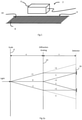
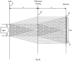
- Figure 2a is a schematic ray diagram illustrating the concept behind this.
- Light from a source e.g. within the readhead
- the diffraction grating diffracts the light into further diffraction orders which recombine at the detector (e.g. a photodiode/sensor array) so as to produce an interference fringe.
- the readhead can record and/or report movement and position by monitoring the movement of the interference fringe across the detector.
- the encoder apparatus is described in US5861953 .
- reference marks can be provided, for instance embedded within the scale's diffraction features, in order to provide defined reference positions.
- Such an encoder apparatus is described in US7659992 .
- Figure 2a is a very simplified illustration of the real optical situation encountered in an encoder apparatus.
- the situation is shown for only one light ray from the source whereas in fact an area of the scale is illuminated by the source. Accordingly, in reality the optical situation shown in Figure 2a is repeated many times over along the length of the scale (i.e. over the area that is illuminated by the source), hence producing a long interference pattern at the detector, which is schematically illustrated in Figure 2b .
- the +/- 1 st orders are shown (e.g. as will be understood the light will be diffracted into multiple orders, e.g. +/- 3 rd , +/- 5 th , etc diffraction orders).
- the ray diagrams are shown as transmissive ray diagrams (that is the light is shown as being transmitted through each of the scale and diffraction grating, whereas in reality at least one of these could be reflective).
- the output of the readhead's detector is used to monitor the relative position of the readhead and scale.
- Such encoders can rely on the recombination of diffracted orders to produce a resultant field at the detector.
- diffraction gratings are configured such that their diffraction features are as equidistantly spaced as possible.
- US5814812 and US5332896 describes an alternative embodiment in which it suggests shifting the diffraction features such that rather than being equidistantly spaced, the spacing between them varies predictably, according to a definite pattern, and in particular, periodically.
- US6094307 relates to a different type of encoder in which the displacement signal is ideally in the form of a triangular-waveform signal proportional to the apparent transparent portion seen from the light source side, wherein the apparent transparent portion varies depending on the degree of overlap between first and second gratings.
- This document discloses a particular amplitude grating having slits which are arranged in a pattern in which the spacings are not constant, but vary in phase, in order to reduce various distortion components in the displacement signal caused by diffraction of light or the like.
- US5696584 and US5559599 describe phase diffraction gratings for optical position encoders wherein the 0 th diffraction order is suppressed and the +/-1 st diffraction orders are maintained.
- US5994692 describes a diffraction grating arrangement wherein the even diffraction orders are suppressed.
- US5113286 also describes a grating for a digital optical system wherein the even orders are suppressed.
- WO2008110239 describes a diffractive component for an interferometer which comprises plural regions of at least a first type and a second type, for generating two or more types of wavefronts serving different functions.
- the present invention relates to an improved optical element that has diffraction features for creating diffraction orders used in the generation of the field detected by the detector.
- the invention relates to an optical element in which the diffraction features are arranged such that they have been shifted from an otherwise nominally regular spaced arrangement.
- an optical element as defined in claim 1.
- the range of the variation in the spacing between the centres of adjacent diffraction features in said series of diffraction features can be not less than 1/200 th of the average period of the diffraction grating's features.
- the optical element can be a diffraction grating for an encoder readhead.
- the diffraction features could be arranged such that the ratio of the intensity of the 1 st order to the 5 th order generated by the optical element is at least 100:1, and/or the ratio of the intensity of the 1 st order to the 7 th order generated by the optical element is at least 150:1.
- the spacing between the centres of adjacent diffraction features can vary irregularly from one pair of adjacent diffraction features to the next along the entire length of the optical element.
- the series of diffraction features can comprise at least five diffraction features.
- an encoder apparatus for determining movement between two relatively moveable parts of an apparatus, the encoder apparatus comprising: a detector; and at least one optical element as defined in claim 1 configured such that said 1 st and selected m th odd numbered diffraction orders contribute to the production at the detector of a signal varying with movement between the two parts.
- a scale/diffraction grating for an encoder is configured to diffract the EMR received from a light source/the scale so as to generate a resultant field, such as an interference fringe or modulate spot(s) at a detector.
- a resultant field such as an interference fringe or modulate spot(s) at a detector.
- the resultant field e.g. the interference fringe or the modulated spot(s)
- the resultant field is primarily formed by the recombining of the +/-1 st diffraction orders from the diffraction grating.
- higher diffraction orders e.g.
- This adverse effect of higher diffraction orders on the generation of interference fringes has been found to increase when the size and/or spacing between optical components such as the detector and a diffraction grating in the readhead and/or scale is reduced (e.g. when trying to reduce the size of the readhead). For example, this can particularly be an issue when the distance between the readhead diffraction grating and detector (shown as "v" in Figures 2 and 3 ) is not more than 10mm, especially not more than 5mm and for example not more than 2mm, for instance 1.8mm or less.
- This adverse effect of higher diffraction orders on the generation of interference fringes has also been found to increase with increases in the nominal period of the scale's diffraction features, e.g. when the nominal period is at least 10 ⁇ m, for example at least 20 ⁇ m, especially at least 30 ⁇ m, for instance at least 40 ⁇ m.
- the adverse effect of higher diffraction orders on the generation of interference fringes has been found to be particularly problematic when the Talbot number of the encoder system falls below 7.25, more particularly below 5, especially below 2 (for example 1.75 or less), and for instance below 1 (for example 0.75 or less).
- ⁇ is the wavelength of the illumination
- u 0 is the distance between the first grating and the second grating (e.g. u in Figures 2a , 2b and 3 )
- pi is the period of the first grating (e.g. the period of the scale 4 in Figures 2a , 2b and 3 )
- p 2 is the period of the second grating (e.g. the period of the diffraction grating 14 in Figures 2a , 2b and 3 ).
- diffraction gratings and/or scales can be designed which minimise the adverse impact of the higher orders on the resultant field.
- the inventors have identified that rather than making the spacing between adjacent diffraction features constant, or even varying in a regular or predictable (e.g. periodic) manner, as is the case with known diffraction gratings, having the freedom so as to shift them from a nominally regular spacing such that the spacing between them (e.g. the spacing between their centres (e.g. their centre of masses) taken along the measuring direction of the scale) can vary selectively, for instance irregularly, can enable selected diffraction orders to be controlled so as to minimise and even substantially eliminate them, whilst substantially maintaining others.
- the exact way in which the spacing between adjacent features will vary can depend on many factors such as the type and configuration of the encoder apparatus as a whole as well as which orders are to be selectively controlled.
- the diffraction features can be shifted from a nominally regular spacing, each feature being shifted by a selected predetermined amount so as to substantially minimise/eliminate at least one odd numbered (e.g. n th ) diffraction order whilst maintaining the existence of the 1 st and at least one other selected odd numbered (e.g. m th ) diffraction order, such that said 1 st and at least one other selected (e.g. m th ) diffraction orders contribute to the production at the detector a signal varying with movement between the two relatively moveable parts of an apparatus.
- odd numbered e.g. n th
- m th selected odd numbered
- the intensity of select diffraction orders can be controlled by shifting the diffraction grating's and/or the scale's features away from a nominally regularly spaced arrangement to one in which the spacing between adjacent diffraction features varies irregularly from one pair of features to the next. This has been found to reduce harmonics in the resultant field at the detector (compared to an encoder apparatus in which a diffraction grating with a constant spacing between diffraction features), resulting in a superior signal output by the detector.
- analysis of the detector's output to determine or monitor the position could be performed within the readhead itself.
- the raw (or conditioned) output of the detector could be output from the readhead to an external processor device which analyses the signal to determine or monitor the relative position of the readhead and scale.
- a series of diffraction features can be a series of features on/in the substrate of the optical element which together diffract incoming EMR into a number of diffraction orders.
- the diffraction features could be marks made on the surface of the optical element's substrate.
- the composition of the optical element's substrate could be manipulated to form the features.
- the shape of the optical element's substrate could be configured to form the diffraction features.
- the shape, size and/or arrangement of diffraction features can vary depending on the particular implementation. Nevertheless, the diffraction features can be generally elongate in shape, for example substantially elliptical or rectangular, with their length extending substantially perpendicular to the encoder apparatus' measurement direction.
- the diffraction features could be in the form of amplitude diffraction features or phase diffraction features. That is for example, the optical element can be an amplitude optical element or a phase optical element, for example an amplitude scale or a phase scale, or an amplitude index grating or a phase index grating.
- the diffraction features of amplitude optical elements e.g.
- phase optical elements e.g. such as phase scales
- phase optical elements e.g. such as phase scales
- phase of EMR e.g. by virtue of the optical element having features with specific thickness, depth, density, material type or the like to control the phase of light
- phase diffraction features modulate the phase of light passing through/reflecting off the optical element to product diffraction orders.
- a combination of phase and amplitude features could be used.
- the encoder apparatus' scale can be an optical element in which its series of consecutive diffraction features comprises at least one set of diffraction features within which the spacing between the centres of adjacent diffraction features varies irregularly from one pair of adjacent diffraction features to the next.
- the scale can comprise a reference mark between two series of consecutive diffraction features. Accordingly, a series of consecutive diffraction features can be delineated by a reference mark.
- a reference mark can be a feature which can be distinguished from the diffraction features.
- a reference mark can be read by a reference mark reading arrangement. Reference marks are typically used to identify "known" or "reference" locations along the length of the scale.
- Such a reference mark reading arrangement might comprise a reference mark sensor that is separate to the above mentioned detector.
- the scale can comprise more than one reference mark.
- a reference mark can be provided adjacent the scale's diffraction features as is commonly known.
- the optical element is a diffraction grating
- the readhead can comprise the detector.
- the readhead can comprise a diffraction grating.
- the diffraction grating can interact with electromagnetic radiation (e.g. from the scale) to produce the signal at the detector (e.g. via effecting the recombination of diffraction orders at the detector).
- the readhead's diffraction grating can be an optical element in which its series of consecutive diffraction features comprises at least one set of diffraction features within which the spacing between the centres of adjacent diffraction features varies irregularly from one pair of adjacent diffraction features to the next.
- the scale and diffraction grating can both comprise said at least one optical element. That is the scale and diffraction grating can both be optical elements in which their series of consecutive diffraction features comprises at least one set of diffraction features within which the spacing between the centres of adjacent diffraction features varies irregularly from one pair of adjacent diffraction features to the next.
- the scale can be the at least one optical element referred to above
- a diffraction grating can be the at least one optical element referred to above
- the scale and a diffraction grating can be the at least one optical element referred to above.
- the range of the variation in the spacing between the centres of adjacent diffraction features in said at least one set of diffraction features can be not less than 1/200 th of the average spacing between the centres of adjacent diffraction features, for instance not less than 1/100 th of the average spacing.
- the range in absolute terms will depend on the system used, but can for example be at least 5 ⁇ m (microns), for instance at least 10 ⁇ m (microns), optionally at least 15 ⁇ m (microns), for instance 17 ⁇ m (microns) or more, and optionally not more than 30 ⁇ m (microns), for example not more than 20 ⁇ m (microns).
- the range of the variation in the spacing between the centres of adjacent diffraction features in said at least one set of diffraction features can be not less than 1/20 th of the average spacing between the centres of adjacent diffraction features, for instance not less than 1/10 th of the average spacing, and optionally not more than 1 ⁇ 2 of the average spacing, for instance not more than 1 ⁇ 4 of the average spacing.
- the average spacing between the centres of adjacent diffraction features in said series of consecutive diffraction features can be, for example, not more than 2mm, more preferably not more than 1mm, especially preferably not more than 0.5mm, and for example can be not less than 500nm, for example not less than 1 ⁇ m (micron).
- the diffraction features can be arranged such that the intensity of at least the +/-5 th and/or 7 th (and/or higher odd orders) diffraction order resulting from the optical element is attenuated compared to a scale having equally, or even predictably or periodically varying, spaced diffraction features.
- the diffraction features can be arranged such that the intensity of at least the +/-5 th and/or 7 th (and/or higher odd orders) diffraction order resulting from the optical element is substantially eliminated.
- the diffraction features can be arranged such that the intensity of at least the +/-5 th diffraction order resulting from the optical element is not more than 0.75%, for example not more than 0.5% of the intensity of the incident light on the optical element, and possibly even less, such as not more than 0.05% of the intensity of the incident light on the optical element.
- the diffraction features can be arranged such that the intensity of at least the +/-7 th diffraction order resulting from the optical element is not more than 0.25%, for example not more than 0.1% of the intensity of the incident light on the optical element, and possibly even less, such as not more than 0.05% (and for example 0.02%, or even 0.015% or less) of the intensity of the incident light on the optical element.
- the diffraction features can be arranged such that the intensity of at least the +/-1 st diffraction order resulting from the optical element is at least 20%, optionally at least 30%, for example 36% or more of the intensity of the incident light on the optical element.
- the diffraction features can be arranged such that the intensity of at least the +/-3 rd diffraction order resulting from the optical element is at least 1%, optionally at least 1.5%, for example 1.9% or more of the intensity of the incident light on the optical element.
- the diffraction features can be arranged such that the intensity of at least the +/-3 rd diffraction order resulting from the optical element is not more than 1%.
- the diffraction features can be arranged such that the ratio of the intensity of the 1 st order to the 5 th order (or indeed any odd diffraction order higher than the 5 th diffraction order) is at least 100:1, optionally at least 200:1, for example at least 300:1, and possibly even more such as at least 700:1.
- the diffraction features can be arranged such that the ratio of the intensity of the 1 st order to the 7 th order (or indeed any higher odd diffraction order) is at least 150:1, optionally at least 300:1, for example at least 500:1, and possibly even more such as at least 1500:1, or higher still such as at least 3000:1.
- the distance between the detector and the diffraction grating can be, for example, not more than 50mm, preferably not more than 10mm, especially preferably not more than 5mm, for example not more than 2mm, for instance 1.8mm or less.
- the readhead can comprise an EMR source (e.g. a light source).
- EMR from the EMR source e.g. light from the light source
- EMR from the EMR source can first interact with the scale to produce diffraction orders before interacting with the diffraction grating to produce further diffraction orders.
- EMR from the EMR source can interact with a diffraction grating prior to the scale (and optionally also with the same or a different diffraction grating after the scale as well).
- the diffraction grating can be configured to interact with EMR (e.g. light) (e.g. from the scale) to produce an interference fringe field at the detector which changes as movement between the scale and readhead occurs. Accordingly, the detector can be configured to output a signal in response to the changing field.
- EMR e.g. light
- the detector can be configured to output a signal in response to the changing field.
- the spacing between adjacent diffraction features can vary irregularly from one pair of adjacent features to the next, such that the signal output by the detector is substantially harmonic free.
- the optical element can comprise at least one consecutive series of diffraction features in which the spacing between the centres of adjacent diffraction features do not vary irregularly from one pair of adjacent diffraction features to the next.
- all of the optical element's diffraction features are arranged such that the spacing between the centres of adjacent diffraction features varies irregularly from one pair of adjacent diffraction features to the next. Accordingly, the spacing between the centres of adjacent diffraction features can vary irregularly from one pair of adjacent diffraction features to the next along the entire length of the optical element.
- the at least one set of diffraction features (within which the spacing between the centres of adjacent diffraction features varies irregularly from one pair to the next) can be repeated at least once along the length of the optical element (i.e. so that there are at least two instances of the same arrangement of diffraction features). Optionally, it can be repeated at least once within said series of consecutive diffraction features.
- the width of diffraction features in the set of diffraction features can be not more than the average spacing between the centres of adjacent diffraction features.
- the width of the diffraction features in said series of consecutive diffraction features can be the same. As will be understood, the widths of the spacing between the diffraction features will vary due to the variation in spacing between them.
- the set of diffraction features can comprise at least five diffraction features, more preferably at least 10 features, for example at least 20 features, for example 30 features (but as will be understood, depending on the particular embodiment could be much more).
- a set of diffraction features can comprise many more diffraction features, such as at least 100 features (but as will be understood, depending on the particular embodiment could be much more, for instance many thousands of features).
- a readhead for an encoder apparatus comprising a detector and a diffraction grating as described in claim 1, configured such that said 1 st and selected m th diffraction orders can contribute to the production of an interference signal at the detector.
- the range of the variation in the spacing between the centres of adjacent diffraction features can be not less than 1/200 th of the average period of the diffraction grating's features.
- the diffraction features could be arranged such that the ratio of the intensity of the 1 st order to the 5 th order generated by the optical element is at least 100:1, and/or the ratio of the intensity of the 1 st order to the 7 th order generated by the optical element is at least 150:1.
- the spacing between the centres of adjacent diffraction features could vary irregularly from one pair of adjacent diffraction features to the next along the entire length of the diffraction grating.
- the diffraction grating could comprise an array of at least five diffraction features.
- a method of manufacturing a diffraction grating for an encoder apparatus comprising determining a select arrangement of diffraction features such that the spacing between the centres of adjacent diffraction features varies such that at least one n th odd numbered diffraction order is substantially eliminated whilst the existence of the 1 st and at least one selected m th odd numbered diffraction order is maintained to such a level that said 1 st and selected m th diffraction orders can contribute to the production of an interference signal at a detector of an encoder apparatus, and forming diffraction features on a substrate according to said select arrangement.
- This application also describes an optical element for generating diffraction orders (e.g. for an encoder apparatus), comprising: an array of diffraction features arranged such that the spacing between the centres of adjacent diffraction features varies irregularly from one pair of adjacent features to the next. In which the spacing between the centres of adjacent diffraction features varies irregularly from one pair of adjacent features to the next, such that the ratio of the intensity of the 1st diffraction order to the 5th diffraction order is at least 100:1, and/or the intensity of the 1st diffraction order to the 7th diffraction order is at least 150:1.
- the optical element can be a diffraction grating for an encoder readhead.
- the optical element can be a scale.
- This application also describes a readhead for an encoder apparatus comprising a detector and a diffraction grating, in which the spacing between the centres of adjacent diffraction features on the diffraction grating varies irregularly from one pair of adjacent features to the next.
- This application also describes a method of manufacturing a diffraction grating for an encoder apparatus comprising determining a select arrangement of diffraction features such that the spacing between the centres of adjacent diffraction features varies irregularly from one pair of adjacent features to the next such that the intensity of the diffraction orders comply with predetermined criteria, and forming diffraction features on a substrate according to said select arrangement.
- predetermined criteria for the intensity of diffraction orders are given above and below in connection with the other aspects of the invention (e.g. the ratios of the intensity of the 1:n th orders).
- This application also describes an optical element for generating diffraction orders for an encoder apparatus, comprising: an array of diffraction features configured such that the ratio of the intensity of the 1st diffraction order to the 5th diffraction order created by the array of diffraction features is at least 100:1.
- the array of diffraction features can be configured in that the spacing between the centres of adjacent diffraction features is chosen for each pair of adjacent diffraction features such that such that the ratio of the intensity of the 1st diffraction order to the 5th diffraction order created by the array of diffraction features is at least 100:1.
- This application also describes an encoder apparatus comprising: a scale having a series of features; a readhead, comprising a detector and a diffraction grating comprising an array of diffraction features arranged such that the spacing between adjacent diffraction features varies irregularly from one pair of adjacent features to the next.
- the encoder apparatus generally designated by reference numeral 2 comprises a scale 4 and a readhead 6.
- the readhead 6 is moveable relative to the scale 4 (although it could be the other way around, or indeed both could be moveable).
- the scale 4 could be mounted to a stationary part of a machine and the readhead 6 mounted to a moveable part of a machine.
- the scale 4 could take many different forms, including for example linear scale as illustrated or rotary scale (e.g. provided on a ring, either on its circumferential edge or on its planar face).
- the scale 4 is an amplitude scale (in that it controls the amplitude of light leaving the scale toward the readhead) and comprises a substrate which has periodic features 10 in the form of dark/relatively non-reflective lines 10 made on an otherwise relatively reflective substrate such that between the periodic features 10 the scale is relatively reflective 8.
- the scale's periodic features could be made in other ways, such as for example by forming relatively reflective lines on an otherwise relatively non-reflective substrate, or even by forming both the relatively reflective and non-reflective lines on a substrate.
- the periodic markings 10 could be provided in other ways, for example, the scale's features or marks could be provided in the form of facets or lines which reflect the light toward and away from the readhead.
- the scale 4 could be a phase scale, in which peaks and pits in the scale modulate the phase of light leaving the scale toward the readhead.
- the scale's substrate is metal, although as will be understood other materials such as glass for instance could be used.
- the periodic marks 10 form the incremental scale facilitating measurement along the X axis (the "measurement dimension").
- a reference mark can be provided either next to or embedded within the periodic marks making up the incremental scale. Details of such reference marks are well known and for instance described in US7659992 , the content of which is incorporated into this specification by this reference.
- the readhead 6 comprises an electromagnetic radiation (“EMR") source, in particular a light source 12, for example a light emitting diode (“LED”), a diffraction grating 14 and a detector 16.
- EMR electromagnetic radiation
- a light source 12 for example a light emitting diode
- LED light emitting diode
- a diffraction grating 14 and a detector 16.
- other components might be present in the readhead, depending on the particular implementation. For instance, a lens might be present, e.g. to collimate the EMR/light from the source.
- the readhead 6 could also comprise components for detecting the reference mark(s), such as a lens and another detector. Again, such a set up is described in US7659992 .
- light from the light source 12 is emitted from the readhead 6 toward the scale 4 through a window 18 in the readhead's housing 11.
- the light has a wavelength in the region of 850nm, but of course this could vary depending on the specific implementation and need not necessarily be visible light but instead could be EMR having a wavelength of anything from 300nm to 2000nm, for example.
- the choice of a suitable wavelength for the source can depend on many factors, including the availability of suitable gratings and detectors that work at the EMR wavelength.
- the light is diffracted and reflected by the scale 4, back through the window 18 toward the diffraction grating 14 where the light is diffracted again before forming a resultant field 40 (see Figure 2b ) (in this case an interference fringe, but could for example be modulated spot(s)) at the detector 16.
- a resultant field 40 in this case an interference fringe, but could for example be modulated spot(s)
- the readhead could be configured such that the diffraction grating 14 is provided on the outermost surface of the readhead and is the component via which light enters the readhead.
- the detector 16 detects the resultant field (e.g. the interference fringes) to produce a signal which is output by the readhead via interface 20 and cable 22 to an external device.
- the resultant field e.g. movement of the interference fringes relative to the detector 16 or a change in intensity of the modulated spot(s)
- the output of can be processed to provide an incremental up/down count which enables an incremental measurement of displacement.
- the resultant field 40 is produced by the recombination of diffracted orders of light from the diffraction grating 14 and scale 4.
- the detector 16 can comprise a plurality of photodiodes, for example.
- the detector 16 can be in the form of an electro-grating, which in other words is a photo-sensor array which can for example comprise two or more sets of interdigitated/interlaced photo-sensitive sensors, each set detecting a different phase of the interference fringe 17 at the detector 16.
- FIG. 10 An example is illustrated in Figure 10 , in which a part of a detector 16 is shown, and in which the photodiodes of four sets of photodiodes A, B, C and D are interdigitated, and the outputs from each photodiode in a set are combined to provide a single output, A', B', C' and D'.
- all the photodiodes in any one set detect the intensity of same phase of the interference fringe (if the fringe period and sensor period are the same).
- This arrangement has the advantage that due to a filtering effect of the optics, the readhead 6 is largely immune to the presence or absence of either of the reflective 8 or non-reflective 10 lines the scale.
- the presence of contamination and/or any reference mark does not significantly affect the interference fringe detected by the detector 16. More details of a scale and readhead of this type are described in US5861953 , the entire contents of which are incorporated into this specification by this reference.
- the electrograting/photo-sensor array can take other forms, such as comprising only three sets of photodiodes that are interdigitated, and different layouts can be used.
- Figure 5 is a schematic plan illustration of a known diffraction grating 114.
- the diffraction grating 114 comprises a series 150 of consecutive diffraction features 130 arranged periodically such that when light passes through the diffracting grating 114 (or is reflected off the diffraction grating), the light is diffracted/split into multiple orders.
- the diffraction features 130 are arranged periodically, that is they occur at a period "p", such that the distance between the centres of adjacent pairs of the same type of feature is constant along the length of the diffraction gating (i.e. is always "s").
- the diffraction grating 114 is not shown to scale and is merely schematic to aid illustration of the invention.
- the diffraction grating is a phase grating.
- the diffraction features 130 manipulate (in other words modulate) the phase of the light passing through/reflected off the diffraction grating in order to create the diffraction orders. This could be achieved for example by the depth of the grating being different at the diffraction features (e.g. the depth of the diffraction grating substrate at the features illustrated by the dark bars 130 could be shallower than that at the features illustrated by the light bars 132).
- the dark 130 and light 132 bars in Figure 2 merely represent regions which affect the phase of light passing through it in to a different extent, e.g. the dark 130 and light 132 bars represent different depths of the diffraction grating's 114 substrate. It could well be, and for example it could be preferable, that the opacity/reflectivity of the diffraction features 130 are the same as the other regions 132 of the diffraction grating 114. As will be understood, other types of diffraction grating include amplitude gratings in which the features manipulate/modulate the amplitude of light passing through/reflected off the diffraction grating in order to create the diffraction orders.
- Figure 6 is a schematic plan illustration of a diffraction grating 14 according to the present invention.
- the diffraction grating 14 comprises a series 50 of consecutive diffraction features 30 arranged and configured such that when light passes through the diffraction grating 14, the light is diffracted/split into multiple orders.
- the diffraction features 30 have been deliberately and selectively shifted from their nominally periodic "p" position such that the spacing "s n " between adjacent diffraction features 30 varies from one pair of diffraction feature to the next. For instance, the distance between the first pair of diffraction features 30 represented by the dark lines is si, whereas the distance between the next pair is s 2 .
- the spacing s n between such adjacent pairs of diffraction features 30 varies irregularly along the length of the scale. That is, the variation in the spacing s n does not change periodically or according to any sort of recognisable pattern.
- the width "w" of the diffraction feature 30 of diffraction grating 14 (that is their size taken in a dimension parallel to the extent of the series of diffraction features ) is constant for all the diffraction features 30. However, this need not necessarily be the case and their widths could vary.
- the dark bars 30 are selected/described as the diffraction features. Nevertheless, as will be understood, the invention is equally applicable if the part of the diffraction grating 14 represented by the light bars 32 are selected/described as the diffraction features. This is because as can be seen the spacing between the centres of the light bars 32 also varies irregularly from one pair to the next. In line with the paragraph above, this also illustrates that the widths of the diffraction features can vary.
- the series 50 of consecutive diffraction features comprises only one set of diffraction features within which the spacing between the centres of adjacent diffraction features varies irregularly from one pair of adjacent diffraction features to the next. That is the length of the set is the same as the length of the series 50, which is also the length of the diffraction grating 14.
- the series 50 of consecutive diffraction features might comprise one or more repeating sets of diffraction features within which the spacing between the centres of adjacent diffraction features varies irregularly from one pair of adjacent diffraction features to the next. This is described in more detail below in connection with the embodiment of Figure 9 .
- Figure 7 is a graph illustrating the variation in spacing between adjacent pairs of the diffraction features 30 of the diffraction grating 14 shown in Figure 6 (which has an average feature spacing of approximately 43 ⁇ m).
- the variation in the spacing is not constant, not constantly increasing or decreasing, and not varying according to some periodic function. Rather, the variation is irregular with no recognisable pattern. As explained below, this is because the position shift of each feature from its nominally periodic position is chosen independently so that they manipulate the diffraction orders as needed (e.g. in order to minimise the intensity of the +/- 5 th order), rather than according to some predetermined function.
- the table below gives an example of another embodiment for a phase diffraction grating according to the invention.
- the table represents the shift of each feature from a nominal feature spacing of 46.67 ⁇ m (micron) (and hence width of 23.34 ⁇ m (micron)) which would be suitable for use in an encoder having an amplitude scale of 40 ⁇ m (micron).
- the spacing between adjacent pairs of diffraction features varies because the diffraction grating has been generated according to a process in which the diffraction features have been deliberately/purposefully shifted from their nominally periodic/regular position by a select amount so as to control the diffraction orders produced by the diffraction grating.
- the process by which the shift of each feature from its nominally periodic/regular position can be determined could for instance involve an iterative algorithm, such as for example a Direct Binary Search. Such a process can involve modelling the behaviour of the encoder system and iteratively going through multiple configurations in order to arrive at an optimum solution via a minimisation process.
- the particular arrangement of the diffraction features 30 on the diffraction grating 14 will depend on many factors including the type of encoder the diffraction grating is to be used in and/or what and/or how the diffraction orders are to be controlled. For instance, in some circumstances it might be desirable to attenuate the +/- 3 rd diffraction order whereas in other circumstances it might be desirable to strengthen the +/- 5 th diffraction order. Accordingly, the particular arrangement of diffraction orders needed to provide for these different scenarios will be different.
- the extent of shift is grossly exaggerated in Figure 6 to aid illustration of the invention.
- the nominal periodic spacing "p" of the diffraction features could be 20 ⁇ m (microns), and the shift of diffraction features from its nominal periodic position could be up to +/- p/2, e.g. in the given example +/- 10 ⁇ m (microns), for example.
- a typical diffraction grating for an encoder readhead might be 2 or 3mm long, and so the typical number diffraction features can be in the order of 100-150.
- the diffraction grating could be even smaller, and for instance between 1mm and 2mm long, such as for example between 1.4mm and 1.5mm long.
- the number of diffraction features can be even smaller, such as somewhere between 25 and 35, for example 30.
- the placement of such diffraction features can be selected so as to control the diffraction orders created by the diffraction grating. Accordingly, for example, as described above it can be preferred that the intensity of the +/- 5 th diffraction order be minimised in order to improve the quality of the resultant field produced at the detector 16, e.g. in order to remove harmonics in the signal produced by the detector 16. It has been found that a diffraction grating according to the present invention can be used to achieve this.
- Figure 8 shows a bar chart illustrating the intensity of different orders (as a percentage of the incident light) produced from a standard diffraction grating in which the spacing between adjacent pairs of diffraction features is constant along the length of the scale, and also the intensity of different orders produced from a diffraction grating according to the invention.
- the intensity of the +/- 5 th and above orders have been significantly reduced compared to the standard grating.
- the diffraction grating 14 has been designed such that there is still some significant +/- 3 rd order as well as +/- 1 st order because it has been found that in some circumstances the +/- 3 rd order can contribute positively to the formation of the interference fringe at the detector 16.
- the bar chart of Figure 8 is marked up with values actually measured from a diffraction grating according to the invention, and values actually measured from a standard diffraction grating.
- the standard diffraction grating is "standard" in that it is the same as the diffraction grating according to the invention (i.e. same material, same feature size, same type (e.g.
- both phase gratings same nominal feature period, etc
- the diffraction features are regularly spaced.
- the intensities of the orders and incident light are measured by placing the diffraction grating into a holding jig.
- Laser light in this case 850nm (nanometres)
- the diffraction orders are measured using a power meter connected to a rotating stage. When the stage moves, a measurement is taken from the power meter and logged to a computer.
- the stage takes a measurement every 0.003 degrees. This produces a large set of power measurements over a given angle range.
- localised averaging of the data can be used. For instance an average of 10 points over 0.03 degrees is taken.
- the intensity of the incident light is measured by the power meter by repeating the above, but where the laser light is arranged to pass light through a blank region of the grating which has no diffraction features.
- other set ups could be used to measure the intensities.
- the grating/jig could be moved instead of/as well as the power meter.
- multiple power meters could be used (e.g. one for each diffraction order to avoid having to provide movement).
- multiple diffraction orders could fall simultaneously on a single CCD (e.g. so that they can be measured simultaneously).
- the diffraction grating according to the invention provides a measured ratio of the intensity of the 1 st order to the 5 th order which is above 800:1, and provides a measured ratio of the intensity of 1 st order to the 7 th order which is above 3000:1:
- it is the diffraction grating's diffraction features that have been arranged such that their spacing varies irregularly in order to improve the signal output by the detector.
- the arrangement shown in Figure 6 could be the scale 4 instead of the diffraction grating 14.
- scales 4 are typically much longer than the diffraction grating (that is even though they can be as small as a few millimetres long, they can be as large as many metres, even tens of metres long) and hence the position of a greater number of features needs to be determined.
- This burden could be reduced by determining the position of a set number of diffraction features along a set length of the optical element (e.g. the scale 4) using the iterative process described above, and then using the results of that process multiple times along the length of the optical element (e.g. the scale 4), e.g. as illustrated in Figure 9 .
- the scale 4 comprises a series 100 of consecutive diffraction features which as shown are delineated by reference marks 102, 103.
- a set 104 of diffraction features within which the spacing between the centres of adjacent diffraction features varies irregularly from one pair of adjacent diffraction features to the next.
- this same set 104 is repeated twice more within the series 100 of consecutive diffraction features.
- the same set 104 is also used in a different series of consecutive diffraction features (subsequent to the second reference mark 103 shown).
- the encoder apparatus comprises a diffraction grating in the readhead, but this need not necessarily be the case. Indeed, it is possible that no diffraction grating is needed at all. In this case the only optical element according to the invention is the scale. Such an encoder is for example described in US2003/0010906 .
- the encoder apparatus could be configured such that the light from the source interacts with a diffraction grating (e.g. in the readhead) before it interacts with a scale (and optionally also interacts with another or the same diffraction grating (e.g. in the readhead) after the scale).
- all of the diffraction grating's diffraction features, and/or the all of the scale's diffraction features are arranged such that their spacing between the centres of adjacent diffraction features varies irregularly from one pair of adjacent diffraction features to the next. This need not be the case. For instance, only some of them need be arranged this way, with the others being arranged with non-irregular spacing, e.g. being constantly spaced.
Landscapes
- Physics & Mathematics (AREA)
- General Physics & Mathematics (AREA)
- Optical Transform (AREA)
- Diffracting Gratings Or Hologram Optical Elements (AREA)
Applications Claiming Priority (4)
| Application Number | Priority Date | Filing Date | Title |
|---|---|---|---|
| EP12250185 | 2012-12-20 | ||
| GBGB1301186.1A GB201301186D0 (en) | 2012-12-20 | 2013-01-23 | Optical element |
| EP13780378.9A EP2936073B1 (en) | 2012-12-20 | 2013-10-15 | Optical element |
| PCT/GB2013/052684 WO2014096764A1 (en) | 2012-12-20 | 2013-10-15 | Optical element |
Related Parent Applications (2)
| Application Number | Title | Priority Date | Filing Date |
|---|---|---|---|
| EP13780378.9A Division EP2936073B1 (en) | 2012-12-20 | 2013-10-15 | Optical element |
| EP13780378.9A Division-Into EP2936073B1 (en) | 2012-12-20 | 2013-10-15 | Optical element |
Publications (2)
| Publication Number | Publication Date |
|---|---|
| EP3564628A1 EP3564628A1 (en) | 2019-11-06 |
| EP3564628B1 true EP3564628B1 (en) | 2022-02-16 |
Family
ID=47713780
Family Applications (2)
| Application Number | Title | Priority Date | Filing Date |
|---|---|---|---|
| EP19172096.0A Active EP3564628B1 (en) | 2012-12-20 | 2013-10-15 | Optical element |
| EP13780378.9A Active EP2936073B1 (en) | 2012-12-20 | 2013-10-15 | Optical element |
Family Applications After (1)
| Application Number | Title | Priority Date | Filing Date |
|---|---|---|---|
| EP13780378.9A Active EP2936073B1 (en) | 2012-12-20 | 2013-10-15 | Optical element |
Country Status (8)
| Country | Link |
|---|---|
| US (2) | US9952068B2 (enExample) |
| EP (2) | EP3564628B1 (enExample) |
| JP (1) | JP6563813B2 (enExample) |
| KR (1) | KR102128135B1 (enExample) |
| CN (1) | CN105008865B (enExample) |
| ES (2) | ES2744978T3 (enExample) |
| GB (1) | GB201301186D0 (enExample) |
| WO (1) | WO2014096764A1 (enExample) |
Families Citing this family (7)
| Publication number | Priority date | Publication date | Assignee | Title |
|---|---|---|---|---|
| JP6957088B2 (ja) * | 2017-04-19 | 2021-11-02 | 株式会社ミツトヨ | 光学式エンコーダ |
| CN109141293B (zh) * | 2018-08-08 | 2020-04-24 | 深圳市银星智能科技股份有限公司 | 基于结构光的物体测量方法及电子设备 |
| US10979248B1 (en) * | 2018-12-26 | 2021-04-13 | Open Invention Network Llc | Onboarding a VNF which includes a VNFC composed of manageable software elements |
| CN111290063A (zh) * | 2019-12-23 | 2020-06-16 | 南开大学 | 一种复振幅调制的介质-金属双层超表面 |
| CN113237498A (zh) * | 2021-05-13 | 2021-08-10 | 华北水利水电大学 | 一种基于平面变周期透射光栅的光学位移传感系统 |
| EP4484898A1 (en) | 2023-06-29 | 2025-01-01 | Renishaw PLC | Encoder apparatus |
| CN118857116B (zh) * | 2024-09-24 | 2025-02-07 | 杭州隆硕科技有限公司 | 一种基于光电反射的位移测量方法、装置、设备及介质 |
Citations (5)
| Publication number | Priority date | Publication date | Assignee | Title |
|---|---|---|---|---|
| US5113286A (en) * | 1990-09-27 | 1992-05-12 | At&T Bell Laboratories | Diffraction grating apparatus and method of forming a surface relief pattern in diffraction grating apparatus |
| US5559599A (en) * | 1993-11-12 | 1996-09-24 | Dr. Johannes Heidenhain Gmbh | Graduation scale having a continuous planar surface with a protective diffusion barrier layer thereon |
| US5696584A (en) * | 1995-01-28 | 1997-12-09 | Johannes Heidenhain Gmbh | Phase grating having an unprotected relief structure with a grating structure that causes destructive interference of reflections |
| US5994692A (en) * | 1995-03-25 | 1999-11-30 | Dr. Johannes Heidenhain Gmbh | Photo-electric position measuring system having a scanning grating with transverse graduations |
| WO2008110239A1 (en) * | 2007-03-15 | 2008-09-18 | Carl Zeiss Smt Ag | Diffractive component, interferometer arrangement, method for qualifying a dual diffraction grating, method of manufacturing an optical element, and interferometric method |
Family Cites Families (22)
| Publication number | Priority date | Publication date | Assignee | Title |
|---|---|---|---|---|
| DE3412128C1 (de) | 1984-03-31 | 1985-05-09 | Dr. Johannes Heidenhain Gmbh, 8225 Traunreut | Positionsmesseinrichtung |
| GB8413955D0 (en) | 1984-05-31 | 1984-07-04 | Pa Consulting Services | Displacement measuring apparatus |
| GB8432574D0 (en) | 1984-12-22 | 1985-02-06 | Renishaw Plc | Opto-electronic scale-reading apparatus |
| JP2539269B2 (ja) * | 1989-07-17 | 1996-10-02 | オークマ株式会社 | 光学式エンコ―ダ |
| JP2575935B2 (ja) | 1990-07-30 | 1997-01-29 | オークマ株式会社 | 位置検出装置 |
| EP0541827B1 (de) * | 1991-11-04 | 1995-04-12 | Dr. Johannes Heidenhain GmbH | Vorrichtung zur Erzeugung oberwellenfreier periodischer Signale |
| DE4436784B4 (de) | 1993-10-26 | 2005-08-18 | Carl Zeiss | Absolutes Positionsmeßsystem |
| JP2695623B2 (ja) | 1994-11-25 | 1998-01-14 | 株式会社ミツトヨ | 光学式エンコーダ |
| GB9424969D0 (en) | 1994-12-10 | 1995-02-08 | Renishaw Plc | Opto-electronic scale reading apparatus |
| JP3215289B2 (ja) * | 1995-04-17 | 2001-10-02 | オークマ株式会社 | スケール及びエンコーダ |
| DE19532246A1 (de) | 1995-09-01 | 1997-03-06 | Heidenhain Gmbh Dr Johannes | Vorrichtung zur Filterung von Oberwellen-Signalanteilen |
| JP3209914B2 (ja) * | 1996-03-19 | 2001-09-17 | オークマ株式会社 | 光学式エンコーダ |
| US6094307A (en) * | 1996-05-17 | 2000-07-25 | Okuma Corporation | Optical grating and encoder |
| DE19726935B4 (de) | 1997-06-25 | 2014-06-12 | Dr. Johannes Heidenhain Gmbh | Optische Positionsmeßeinrichtung |
| EP0896206B1 (de) | 1997-08-07 | 2002-12-11 | Dr. Johannes Heidenhain GmbH | Abtasteinheit für eine optische Positionsmesseinrichtung |
| US6723980B2 (en) | 2001-07-16 | 2004-04-20 | Wai-Hon Lee | Position sensor with grating to detect moving object with periodic pattern |
| DE10347604A1 (de) | 2003-10-14 | 2005-05-12 | Heidenhain Gmbh Dr Johannes | Optische Positionsmesseinrichtung |
| GB0413710D0 (en) | 2004-06-21 | 2004-07-21 | Renishaw Plc | Scale reading apparatus |
| GB0613902D0 (en) * | 2006-07-13 | 2006-08-23 | Renishaw Plc | Scale and readhead |
| JP5011201B2 (ja) | 2008-05-01 | 2012-08-29 | 株式会社ミツトヨ | 絶対位置測長型エンコーダ |
| ES2758525T3 (es) | 2008-12-17 | 2020-05-05 | Fagor Automation S Coop | Encoder de posición absoluta |
| ITMI20110562A1 (it) | 2011-04-06 | 2012-10-07 | Comelz Spa | Procedimento e dispositivo di rilevamento di posizione di un organo trasportatore. |
-
2013
- 2013-01-23 GB GBGB1301186.1A patent/GB201301186D0/en not_active Ceased
- 2013-10-15 ES ES13780378T patent/ES2744978T3/es active Active
- 2013-10-15 JP JP2015548743A patent/JP6563813B2/ja active Active
- 2013-10-15 EP EP19172096.0A patent/EP3564628B1/en active Active
- 2013-10-15 KR KR1020157019443A patent/KR102128135B1/ko active Active
- 2013-10-15 WO PCT/GB2013/052684 patent/WO2014096764A1/en not_active Ceased
- 2013-10-15 CN CN201380072987.1A patent/CN105008865B/zh active Active
- 2013-10-15 EP EP13780378.9A patent/EP2936073B1/en active Active
- 2013-10-15 ES ES19172096T patent/ES2909008T3/es active Active
- 2013-10-15 US US14/651,495 patent/US9952068B2/en active Active
-
2018
- 2018-03-19 US US15/925,002 patent/US10768026B2/en active Active
Patent Citations (5)
| Publication number | Priority date | Publication date | Assignee | Title |
|---|---|---|---|---|
| US5113286A (en) * | 1990-09-27 | 1992-05-12 | At&T Bell Laboratories | Diffraction grating apparatus and method of forming a surface relief pattern in diffraction grating apparatus |
| US5559599A (en) * | 1993-11-12 | 1996-09-24 | Dr. Johannes Heidenhain Gmbh | Graduation scale having a continuous planar surface with a protective diffusion barrier layer thereon |
| US5696584A (en) * | 1995-01-28 | 1997-12-09 | Johannes Heidenhain Gmbh | Phase grating having an unprotected relief structure with a grating structure that causes destructive interference of reflections |
| US5994692A (en) * | 1995-03-25 | 1999-11-30 | Dr. Johannes Heidenhain Gmbh | Photo-electric position measuring system having a scanning grating with transverse graduations |
| WO2008110239A1 (en) * | 2007-03-15 | 2008-09-18 | Carl Zeiss Smt Ag | Diffractive component, interferometer arrangement, method for qualifying a dual diffraction grating, method of manufacturing an optical element, and interferometric method |
Also Published As
| Publication number | Publication date |
|---|---|
| ES2744978T3 (es) | 2020-02-27 |
| JP6563813B2 (ja) | 2019-08-21 |
| US10768026B2 (en) | 2020-09-08 |
| JP2016506516A (ja) | 2016-03-03 |
| WO2014096764A1 (en) | 2014-06-26 |
| CN105008865A (zh) | 2015-10-28 |
| CN105008865B (zh) | 2017-10-20 |
| KR102128135B1 (ko) | 2020-06-29 |
| US9952068B2 (en) | 2018-04-24 |
| EP2936073A1 (en) | 2015-10-28 |
| ES2909008T3 (es) | 2022-05-04 |
| EP3564628A1 (en) | 2019-11-06 |
| US20180209824A1 (en) | 2018-07-26 |
| KR20150097738A (ko) | 2015-08-26 |
| US20150308865A1 (en) | 2015-10-29 |
| EP2936073B1 (en) | 2019-06-12 |
| GB201301186D0 (en) | 2013-03-06 |
Similar Documents
| Publication | Publication Date | Title |
|---|---|---|
| US10768026B2 (en) | Optical element | |
| EP3347681B1 (en) | Encoder apparatus | |
| EP3052897B1 (en) | Measurement encoder | |
| KR101240413B1 (ko) | 원점 검출 장치, 변위 측정 장치 및 광학 장치 | |
| EP3052898B1 (en) | Reference mark detector arrangement | |
| EP2889586B1 (en) | Optical encoder | |
| JP5974329B2 (ja) | 光電式エンコーダ | |
| JP5046523B2 (ja) | 位置測定装置 | |
| EP3052896A1 (en) | Position measurement encoder | |
| CN107044861B (zh) | 光电式编码器 | |
| EP3850310B1 (en) | Measurement device | |
| JP6684087B2 (ja) | 光エンコーダ | |
| EP4390326A1 (en) | Encoder apparatus | |
| JP5154072B2 (ja) | 光電式エンコーダ | |
| JP4543311B2 (ja) | 光学式エンコーダ | |
| EP3527953B1 (en) | Methods to calculate the shape of a mask slots of an optical incremental encoder | |
| EP4639092A1 (en) | Encoder apparatus | |
| JP7066264B2 (ja) | エンコーダおよびエンコーダの制御方法 | |
| JP2021193354A (ja) | 光学式エンコーダ及び制御装置 |
Legal Events
| Date | Code | Title | Description |
|---|---|---|---|
| PUAI | Public reference made under article 153(3) epc to a published international application that has entered the european phase |
Free format text: ORIGINAL CODE: 0009012 |
|
| STAA | Information on the status of an ep patent application or granted ep patent |
Free format text: STATUS: THE APPLICATION HAS BEEN PUBLISHED |
|
| AC | Divisional application: reference to earlier application |
Ref document number: 2936073 Country of ref document: EP Kind code of ref document: P |
|
| AK | Designated contracting states |
Kind code of ref document: A1 Designated state(s): AL AT BE BG CH CY CZ DE DK EE ES FI FR GB GR HR HU IE IS IT LI LT LU LV MC MK MT NL NO PL PT RO RS SE SI SK SM TR |
|
| STAA | Information on the status of an ep patent application or granted ep patent |
Free format text: STATUS: REQUEST FOR EXAMINATION WAS MADE |
|
| 17P | Request for examination filed |
Effective date: 20200505 |
|
| RBV | Designated contracting states (corrected) |
Designated state(s): AL AT BE BG CH CY CZ DE DK EE ES FI FR GB GR HR HU IE IS IT LI LT LU LV MC MK MT NL NO PL PT RO RS SE SI SK SM TR |
|
| STAA | Information on the status of an ep patent application or granted ep patent |
Free format text: STATUS: EXAMINATION IS IN PROGRESS |
|
| 17Q | First examination report despatched |
Effective date: 20200708 |
|
| GRAJ | Information related to disapproval of communication of intention to grant by the applicant or resumption of examination proceedings by the epo deleted |
Free format text: ORIGINAL CODE: EPIDOSDIGR1 |
|
| GRAP | Despatch of communication of intention to grant a patent |
Free format text: ORIGINAL CODE: EPIDOSNIGR1 |
|
| GRAP | Despatch of communication of intention to grant a patent |
Free format text: ORIGINAL CODE: EPIDOSNIGR1 |
|
| STAA | Information on the status of an ep patent application or granted ep patent |
Free format text: STATUS: GRANT OF PATENT IS INTENDED |
|
| INTG | Intention to grant announced |
Effective date: 20211001 |
|
| GRAS | Grant fee paid |
Free format text: ORIGINAL CODE: EPIDOSNIGR3 |
|
| GRAA | (expected) grant |
Free format text: ORIGINAL CODE: 0009210 |
|
| STAA | Information on the status of an ep patent application or granted ep patent |
Free format text: STATUS: THE PATENT HAS BEEN GRANTED |
|
| AC | Divisional application: reference to earlier application |
Ref document number: 2936073 Country of ref document: EP Kind code of ref document: P |
|
| AK | Designated contracting states |
Kind code of ref document: B1 Designated state(s): AL AT BE BG CH CY CZ DE DK EE ES FI FR GB GR HR HU IE IS IT LI LT LU LV MC MK MT NL NO PL PT RO RS SE SI SK SM TR |
|
| REG | Reference to a national code |
Ref country code: GB Ref legal event code: FG4D |
|
| REG | Reference to a national code |
Ref country code: CH Ref legal event code: EP |
|
| REG | Reference to a national code |
Ref country code: DE Ref legal event code: R096 Ref document number: 602013080940 Country of ref document: DE |
|
| REG | Reference to a national code |
Ref country code: AT Ref legal event code: REF Ref document number: 1469156 Country of ref document: AT Kind code of ref document: T Effective date: 20220315 |
|
| REG | Reference to a national code |
Ref country code: IE Ref legal event code: FG4D |
|
| REG | Reference to a national code |
Ref country code: ES Ref legal event code: FG2A Ref document number: 2909008 Country of ref document: ES Kind code of ref document: T3 Effective date: 20220504 |
|
| REG | Reference to a national code |
Ref country code: LT Ref legal event code: MG9D |
|
| REG | Reference to a national code |
Ref country code: NL Ref legal event code: MP Effective date: 20220216 |
|
| PG25 | Lapsed in a contracting state [announced via postgrant information from national office to epo] |
Ref country code: SE Free format text: LAPSE BECAUSE OF FAILURE TO SUBMIT A TRANSLATION OF THE DESCRIPTION OR TO PAY THE FEE WITHIN THE PRESCRIBED TIME-LIMIT Effective date: 20220216 Ref country code: RS Free format text: LAPSE BECAUSE OF FAILURE TO SUBMIT A TRANSLATION OF THE DESCRIPTION OR TO PAY THE FEE WITHIN THE PRESCRIBED TIME-LIMIT Effective date: 20220216 Ref country code: PT Free format text: LAPSE BECAUSE OF FAILURE TO SUBMIT A TRANSLATION OF THE DESCRIPTION OR TO PAY THE FEE WITHIN THE PRESCRIBED TIME-LIMIT Effective date: 20220616 Ref country code: NO Free format text: LAPSE BECAUSE OF FAILURE TO SUBMIT A TRANSLATION OF THE DESCRIPTION OR TO PAY THE FEE WITHIN THE PRESCRIBED TIME-LIMIT Effective date: 20220516 Ref country code: NL Free format text: LAPSE BECAUSE OF FAILURE TO SUBMIT A TRANSLATION OF THE DESCRIPTION OR TO PAY THE FEE WITHIN THE PRESCRIBED TIME-LIMIT Effective date: 20220216 Ref country code: LT Free format text: LAPSE BECAUSE OF FAILURE TO SUBMIT A TRANSLATION OF THE DESCRIPTION OR TO PAY THE FEE WITHIN THE PRESCRIBED TIME-LIMIT Effective date: 20220216 Ref country code: HR Free format text: LAPSE BECAUSE OF FAILURE TO SUBMIT A TRANSLATION OF THE DESCRIPTION OR TO PAY THE FEE WITHIN THE PRESCRIBED TIME-LIMIT Effective date: 20220216 Ref country code: BG Free format text: LAPSE BECAUSE OF FAILURE TO SUBMIT A TRANSLATION OF THE DESCRIPTION OR TO PAY THE FEE WITHIN THE PRESCRIBED TIME-LIMIT Effective date: 20220516 |
|
| PG25 | Lapsed in a contracting state [announced via postgrant information from national office to epo] |
Ref country code: PL Free format text: LAPSE BECAUSE OF FAILURE TO SUBMIT A TRANSLATION OF THE DESCRIPTION OR TO PAY THE FEE WITHIN THE PRESCRIBED TIME-LIMIT Effective date: 20220216 Ref country code: LV Free format text: LAPSE BECAUSE OF FAILURE TO SUBMIT A TRANSLATION OF THE DESCRIPTION OR TO PAY THE FEE WITHIN THE PRESCRIBED TIME-LIMIT Effective date: 20220216 Ref country code: GR Free format text: LAPSE BECAUSE OF FAILURE TO SUBMIT A TRANSLATION OF THE DESCRIPTION OR TO PAY THE FEE WITHIN THE PRESCRIBED TIME-LIMIT Effective date: 20220517 Ref country code: FI Free format text: LAPSE BECAUSE OF FAILURE TO SUBMIT A TRANSLATION OF THE DESCRIPTION OR TO PAY THE FEE WITHIN THE PRESCRIBED TIME-LIMIT Effective date: 20220216 |
|
| PG25 | Lapsed in a contracting state [announced via postgrant information from national office to epo] |
Ref country code: IS Free format text: LAPSE BECAUSE OF FAILURE TO SUBMIT A TRANSLATION OF THE DESCRIPTION OR TO PAY THE FEE WITHIN THE PRESCRIBED TIME-LIMIT Effective date: 20220617 |
|
| PG25 | Lapsed in a contracting state [announced via postgrant information from national office to epo] |
Ref country code: SM Free format text: LAPSE BECAUSE OF FAILURE TO SUBMIT A TRANSLATION OF THE DESCRIPTION OR TO PAY THE FEE WITHIN THE PRESCRIBED TIME-LIMIT Effective date: 20220216 Ref country code: SK Free format text: LAPSE BECAUSE OF FAILURE TO SUBMIT A TRANSLATION OF THE DESCRIPTION OR TO PAY THE FEE WITHIN THE PRESCRIBED TIME-LIMIT Effective date: 20220216 Ref country code: RO Free format text: LAPSE BECAUSE OF FAILURE TO SUBMIT A TRANSLATION OF THE DESCRIPTION OR TO PAY THE FEE WITHIN THE PRESCRIBED TIME-LIMIT Effective date: 20220216 Ref country code: EE Free format text: LAPSE BECAUSE OF FAILURE TO SUBMIT A TRANSLATION OF THE DESCRIPTION OR TO PAY THE FEE WITHIN THE PRESCRIBED TIME-LIMIT Effective date: 20220216 Ref country code: DK Free format text: LAPSE BECAUSE OF FAILURE TO SUBMIT A TRANSLATION OF THE DESCRIPTION OR TO PAY THE FEE WITHIN THE PRESCRIBED TIME-LIMIT Effective date: 20220216 Ref country code: CZ Free format text: LAPSE BECAUSE OF FAILURE TO SUBMIT A TRANSLATION OF THE DESCRIPTION OR TO PAY THE FEE WITHIN THE PRESCRIBED TIME-LIMIT Effective date: 20220216 |
|
| REG | Reference to a national code |
Ref country code: DE Ref legal event code: R097 Ref document number: 602013080940 Country of ref document: DE |
|
| PG25 | Lapsed in a contracting state [announced via postgrant information from national office to epo] |
Ref country code: AL Free format text: LAPSE BECAUSE OF FAILURE TO SUBMIT A TRANSLATION OF THE DESCRIPTION OR TO PAY THE FEE WITHIN THE PRESCRIBED TIME-LIMIT Effective date: 20220216 |
|
| PLBE | No opposition filed within time limit |
Free format text: ORIGINAL CODE: 0009261 |
|
| STAA | Information on the status of an ep patent application or granted ep patent |
Free format text: STATUS: NO OPPOSITION FILED WITHIN TIME LIMIT |
|
| 26N | No opposition filed |
Effective date: 20221117 |
|
| PG25 | Lapsed in a contracting state [announced via postgrant information from national office to epo] |
Ref country code: SI Free format text: LAPSE BECAUSE OF FAILURE TO SUBMIT A TRANSLATION OF THE DESCRIPTION OR TO PAY THE FEE WITHIN THE PRESCRIBED TIME-LIMIT Effective date: 20220216 |
|
| PG25 | Lapsed in a contracting state [announced via postgrant information from national office to epo] |
Ref country code: MC Free format text: LAPSE BECAUSE OF FAILURE TO SUBMIT A TRANSLATION OF THE DESCRIPTION OR TO PAY THE FEE WITHIN THE PRESCRIBED TIME-LIMIT Effective date: 20220216 |
|
| REG | Reference to a national code |
Ref country code: AT Ref legal event code: UEP Ref document number: 1469156 Country of ref document: AT Kind code of ref document: T Effective date: 20220216 |
|
| REG | Reference to a national code |
Ref country code: BE Ref legal event code: MM Effective date: 20221031 |
|
| PG25 | Lapsed in a contracting state [announced via postgrant information from national office to epo] |
Ref country code: LU Free format text: LAPSE BECAUSE OF NON-PAYMENT OF DUE FEES Effective date: 20221015 |
|
| P01 | Opt-out of the competence of the unified patent court (upc) registered |
Effective date: 20230602 |
|
| PG25 | Lapsed in a contracting state [announced via postgrant information from national office to epo] |
Ref country code: BE Free format text: LAPSE BECAUSE OF NON-PAYMENT OF DUE FEES Effective date: 20221031 |
|
| PG25 | Lapsed in a contracting state [announced via postgrant information from national office to epo] |
Ref country code: IE Free format text: LAPSE BECAUSE OF NON-PAYMENT OF DUE FEES Effective date: 20221015 |
|
| PG25 | Lapsed in a contracting state [announced via postgrant information from national office to epo] |
Ref country code: HU Free format text: LAPSE BECAUSE OF FAILURE TO SUBMIT A TRANSLATION OF THE DESCRIPTION OR TO PAY THE FEE WITHIN THE PRESCRIBED TIME-LIMIT; INVALID AB INITIO Effective date: 20131015 |
|
| PG25 | Lapsed in a contracting state [announced via postgrant information from national office to epo] |
Ref country code: CY Free format text: LAPSE BECAUSE OF FAILURE TO SUBMIT A TRANSLATION OF THE DESCRIPTION OR TO PAY THE FEE WITHIN THE PRESCRIBED TIME-LIMIT Effective date: 20220216 |
|
| PG25 | Lapsed in a contracting state [announced via postgrant information from national office to epo] |
Ref country code: MK Free format text: LAPSE BECAUSE OF FAILURE TO SUBMIT A TRANSLATION OF THE DESCRIPTION OR TO PAY THE FEE WITHIN THE PRESCRIBED TIME-LIMIT Effective date: 20220216 |
|
| PG25 | Lapsed in a contracting state [announced via postgrant information from national office to epo] |
Ref country code: TR Free format text: LAPSE BECAUSE OF FAILURE TO SUBMIT A TRANSLATION OF THE DESCRIPTION OR TO PAY THE FEE WITHIN THE PRESCRIBED TIME-LIMIT Effective date: 20220216 |
|
| PG25 | Lapsed in a contracting state [announced via postgrant information from national office to epo] |
Ref country code: MT Free format text: LAPSE BECAUSE OF FAILURE TO SUBMIT A TRANSLATION OF THE DESCRIPTION OR TO PAY THE FEE WITHIN THE PRESCRIBED TIME-LIMIT Effective date: 20220216 |
|
| PGFP | Annual fee paid to national office [announced via postgrant information from national office to epo] |
Ref country code: DE Payment date: 20241029 Year of fee payment: 12 |
|
| PGFP | Annual fee paid to national office [announced via postgrant information from national office to epo] |
Ref country code: GB Payment date: 20241022 Year of fee payment: 12 |
|
| PGFP | Annual fee paid to national office [announced via postgrant information from national office to epo] |
Ref country code: FR Payment date: 20241025 Year of fee payment: 12 Ref country code: AT Payment date: 20241018 Year of fee payment: 12 |
|
| PGFP | Annual fee paid to national office [announced via postgrant information from national office to epo] |
Ref country code: IT Payment date: 20241022 Year of fee payment: 12 Ref country code: ES Payment date: 20241118 Year of fee payment: 12 |
|
| PGFP | Annual fee paid to national office [announced via postgrant information from national office to epo] |
Ref country code: CH Payment date: 20241101 Year of fee payment: 12 |
|
| REG | Reference to a national code |
Ref country code: CH Ref legal event code: U11 Free format text: ST27 STATUS EVENT CODE: U-0-0-U10-U11 (AS PROVIDED BY THE NATIONAL OFFICE) Effective date: 20251101 |