EP3560085B1 - Improvements in single inductor multiple output regulators - Google Patents
Improvements in single inductor multiple output regulators Download PDFInfo
- Publication number
- EP3560085B1 EP3560085B1 EP16819575.8A EP16819575A EP3560085B1 EP 3560085 B1 EP3560085 B1 EP 3560085B1 EP 16819575 A EP16819575 A EP 16819575A EP 3560085 B1 EP3560085 B1 EP 3560085B1
- Authority
- EP
- European Patent Office
- Prior art keywords
- output
- voltage
- error voltage
- control circuit
- operable
- Prior art date
- Legal status (The legal status is an assumption and is not a legal conclusion. Google has not performed a legal analysis and makes no representation as to the accuracy of the status listed.)
- Active
Links
Images


Classifications
-
- H—ELECTRICITY
- H02—GENERATION; CONVERSION OR DISTRIBUTION OF ELECTRIC POWER
- H02M—APPARATUS FOR CONVERSION BETWEEN AC AND AC, BETWEEN AC AND DC, OR BETWEEN DC AND DC, AND FOR USE WITH MAINS OR SIMILAR POWER SUPPLY SYSTEMS; CONVERSION OF DC OR AC INPUT POWER INTO SURGE OUTPUT POWER; CONTROL OR REGULATION THEREOF
- H02M3/00—Conversion of DC power input into DC power output
- H02M3/02—Conversion of DC power input into DC power output without intermediate conversion into AC
- H02M3/04—Conversion of DC power input into DC power output without intermediate conversion into AC by static converters
- H02M3/10—Conversion of DC power input into DC power output without intermediate conversion into AC by static converters using discharge tubes with control electrode or semiconductor devices with control electrode
- H02M3/145—Conversion of DC power input into DC power output without intermediate conversion into AC by static converters using discharge tubes with control electrode or semiconductor devices with control electrode using devices of a triode or transistor type requiring continuous application of a control signal
- H02M3/155—Conversion of DC power input into DC power output without intermediate conversion into AC by static converters using discharge tubes with control electrode or semiconductor devices with control electrode using devices of a triode or transistor type requiring continuous application of a control signal using semiconductor devices only
- H02M3/156—Conversion of DC power input into DC power output without intermediate conversion into AC by static converters using discharge tubes with control electrode or semiconductor devices with control electrode using devices of a triode or transistor type requiring continuous application of a control signal using semiconductor devices only with automatic control of output voltage or current, e.g. switching regulators
- H02M3/158—Conversion of DC power input into DC power output without intermediate conversion into AC by static converters using discharge tubes with control electrode or semiconductor devices with control electrode using devices of a triode or transistor type requiring continuous application of a control signal using semiconductor devices only with automatic control of output voltage or current, e.g. switching regulators including plural semiconductor devices as final control devices for a single load
- H02M3/1582—Buck-boost converters
-
- G—PHYSICS
- G05—CONTROLLING; REGULATING
- G05F—SYSTEMS FOR REGULATING ELECTRIC OR MAGNETIC VARIABLES
- G05F1/00—Automatic systems in which deviations of an electric quantity from one or more predetermined values are detected at the output of the system and fed back to a device within the system to restore the detected quantity to its predetermined value or values, i.e. retroactive systems
- G05F1/10—Regulating voltage or current
- G05F1/46—Regulating voltage or current wherein the variable actually regulated by the final control device is DC
-
- H—ELECTRICITY
- H02—GENERATION; CONVERSION OR DISTRIBUTION OF ELECTRIC POWER
- H02M—APPARATUS FOR CONVERSION BETWEEN AC AND AC, BETWEEN AC AND DC, OR BETWEEN DC AND DC, AND FOR USE WITH MAINS OR SIMILAR POWER SUPPLY SYSTEMS; CONVERSION OF DC OR AC INPUT POWER INTO SURGE OUTPUT POWER; CONTROL OR REGULATION THEREOF
- H02M1/00—Details of apparatus for conversion
- H02M1/0083—Converters characterised by their input or output configuration
- H02M1/009—Converters characterised by their input or output configuration having two or more independently controlled outputs
Definitions
- the present invention relates to control circuits for voltage regulators and in particular to control circuits for a single inductor multiple output voltage regulator operable to provide an independent regulated voltage at each of a plurality of outputs using a single inductor.
- Single-Inductor Single-Output (SISO) DC-DC converters otherwise known as DC-DC switching regulators, are well known in the art. Switches are used to appropriately store and release energy in the inductor using non-overlapping phases that are a fraction (each typically approximately one half) of the switching period.
- the circuits include a feedback control-loop to ensure the output is as close as possible to the required voltage level. Examples include step-down (buck), step-up (boost) and buck-boost DC-DC converters or switching regulators.
- DC-DC switching regulators capable of providing two or more outputs with an independent DC voltage
- Such topologies known as Single Inductor Multiple Output (SIMO) regulators
- SIMO Single Inductor Multiple Output
- Such topologies known as Single Inductor Multiple Output (SIMO) regulators
- SIMO Single Inductor Multiple Output
- Such regulators operate by allowing the single inductor to be time-shared amongst two or more outputs through deployment of additional switches on the output side of the inductor.
- US patent application US2014/225577 describes a buck-boost regulation methodology operable, in one embodiment, with a single inductor, four-switch buck-boost regulator configured for discontinuous conduction mode.
- control circuit for a single inductor multiple output voltage regulator, the voltage regulator comprising an inductor and being operable to provide an independent regulated voltage at each of a plurality of outputs
- the control circuit comprising: output switches for selective connection of each output to a first inductor terminal of the inductor; and a controller operable to control said output switches in a plurality of switching periods, such that, in a first operational state, each output is periodically connected to the first inductor terminal for a respective connected time duration to generate said regulated voltage at that output, wherein the controller is operable to designate one of said outputs as a priority output, said priority output being the output for which at least a first portion of its corresponding connected time duration is first calculated, said controller being further operable such that the priority output designation is periodically switched to a different one of said outputs.
- control circuit for a single inductor multiple output voltage regulator, the control circuit comprising an inductor and being operable to provide an independent regulated voltage at each of a plurality of outputs, the control circuit comprising: output switches for selective connection of each output to a first inductor terminal of the inductor; and a controller operable to control said output switches in a plurality of switching periods such that, in a first operational state, each output is periodically connected to the first inductor terminal for a respective connected time duration to generate said regulated voltage at that output; said controller being further operable to: determine whether the voltage regulator is in a locked condition; determine whether the locked condition is valid; and if the locked condition is invalid, to use a respective alternative voltage regulator to supply one or more of the outputs.
- a single inductor multiple output voltage regulator operable to provide an independent regulated voltage at each of a plurality of outputs, comprising: the control circuit of the first aspect; and said inductor.
- Described herein are methods for reducing cross-regulation and/or increasing stability of a single inductor multiple output voltage regulator, and single inductor multiple output voltage regulators implementing such methods.
- the proposed method is herein described as a Charge Controlled Energizing Cycle per Switching Period (CCECSP) method, and is suitable for driving a set of switches to obtain a SIMO DC-DC regulator.
- CCECSP Charge Controlled Energizing Cycle per Switching Period
- buck SIMO DC-DC regulator buck SIMO DC-DC regulator; however it will be readily apparent that the disclosure is not limited to such, and is equally applicable to a boost SIMO DC-DC regulator or to a buck-boost SIMO DC-DC regulator.
- the regulator may generate two or more independent output voltages.
- the independent output voltages may be all at different voltage levels, or two (or more) of the independent output voltages may be at the same level.
- FIG. 1 illustrates a SIMO regulator capable of regulating two independent outputs according to the concepts described herein.
- Such regulators are sometimes referred to as single inductor dual output (SIDO) regulators.
- the buck regulator comprises a pair of input side electronic switches 101 and a pair of output side switches 102 as illustrated. It should be noted that regulators with more than two outputs would require additional switches, at least one extra switch per output, along with additional voltage and current sensing connections for each output.
- An additional low dropout regulator (LDO) circuit may also be provided for each of the additional outputs.
- LDO low dropout regulator
- the output side switches 102 selectively connect a first inductor terminal 104a of an inductor 104 having inductance L to a respective output: specifically first output side switch SW1 connects the inductor to first output 114 and second output side switch SW2 connects the inductor to second output 115.
- Input side switches 101 selectively connect a second terminal 104b of the inductor 104 to one of two supply voltages, and comprise a high-side switch HS which is responsible for allowing current to flow from voltage supply VDD 103 through the inductor 104, and a low-side switch LS which is responsible for allowing current to flow from the inductor 104 toward voltage supply VSS 105.
- a finite state machine (FSM) 106 receives digital signals representative of the voltages sensed at each output, having been digitised by respective analogue-to-digital converters (ADCs), specifically ADC1 107 and ADC2 108. Further inputs to FSM 106 are provided by a set of interrupt triggering signals from Over Current Detector (OCD) 109, Zero Current Detector (ZCD) 110, Over Voltage Detector (OVD) 111 and Under Voltage Detector (UVD) 112; and from low-dropout regulator (LDO) circuits 113.
- OCD Over Current Detector
- ZCD Zero Current Detector
- OLED Over Voltage Detector
- UVD Under Voltage Detector
- LDO low-dropout regulator
- the output loads for each output are represented by a respective capacitor (C 1 , C 2 ) and resistor (R 1 , R 2 ) pair connected in parallel for the first output 114 and second output 115, respectively.
- a bridge capacitor C ER 116 is connected between the outputs 114, 115 in order to decrease the equivalent series resistance (ESR) effect due to each output load's capacitor (C 1 , C 2 ). Additionally, the bridge capacitor 116 decreases the voltage drop on the opposite output, thereby reducing cross-correlation.
- a capacitor switching network may be provided for switching the bridge capacitor between the two outputs having switching transition 180 degrees out of phase at any instant. The FSM 106 will know which transitions occur, and therefore can control the capacitor switching network accordingly.
- OCD 109, ZCD 110, OVD 111 and UVD 112 may each comprise an open-loop comparator based detection circuit.
- Each detection circuit may comprise a sensor (voltage sensor or current sensor as appropriate) to obtain a sensed (voltage or current) value.
- the open-loop comparator translates this sensed value into a binary indicator by comparing the sensed value to a corresponding threshold.
- the binary indicator will be set to an appropriate value indicating either a normal condition or an abnormal condition (i.e., over current condition, zero current condition, over voltage condition or under voltage condition as appropriate).
- an appropriate interrupt may be generated and stored in a "current state" register of the FSM 106. When an interrupt is detected, the FSM 106 transitions to a corresponding state as described in the next section and illustrated in Figure 3 .
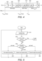
- FIG. 2 illustrates an example sequence of operational states according to FSM 106. Following a "reset” state 200, the state of the FSM proceeds to a "trigger" state 210. In “trigger” state 210, all analogue circuits are initialized to ensure that they fully enter into a regime status. After this state, the FSM transitions to a "start-up" state 220 and remains in this state until a first voltage level of at least one of the outputs 114, 115 exceeds a required voltage level.
- the FSM 106 enters into a "steady-state" state 230, during which instant the timings of the charging and discharging cycles for each of the outputs 114, 115 are determined according to the CCECSP algorithm implemented in the FSM 106.
- this "steady-state” state the FSM 106 adaptively maintains the voltage developed across each output 114, 115 at the required level.
- the actions taken in each of these states are similar except that they relate to different outputs, i.e.
- a switching sequence defines a respective time duration in which the inductor is connected to each output.
- the "connected time duration" for a particular output is the time duration that the inductor is connected to that output.
- the connected time duration for each output will comprise a charging phase and discharging phase corresponding to that output, each of variable duration.
- the connected time duration corresponding to each output will be variable with their sum always being equal to the switching period T sw .
- the charging phase and discharging phase of a connected time duration may comprise adjacent slots in a time period, or their slots may be separated by charging and/or discharging phases corresponding to other outputs.
- the order of the charging phase and discharge phase of a particular connected time duration within a switching period can be varied and/or is arbitrary.
- the time duration of the connection for the first output comprises the sum of a first charging phase time duration ta and a first discharging phase time duration td
- the connected time duration for the second output comprises the sum of a second charging phase time duration tb and a second discharging phase time duration tc.
- Figure 3(a) illustrates such operation. It shows (top) the inductor current against time during a switching period divided into the four phases of respective durations ta, tb, tc, td, and below this the corresponding switch control signals for switches HS, LS, SW1, SW2 over the same time.
- the four different phases comprise, more specifically:
- FIG. 3(b) illustrates the switching sequence in an OCD or OVD interrupt state.
- the interrupt has been called from the first output 114.
- the duration of discharging phase ta is shorter than that of charging phase td.
- the OCD circuit remains active. This enables the determination of whether, by the end of the OCD interrupt state switching period, the sensed current has returned to a normal condition or remains in an abnormal (over current) condition.
- Determination as to whether the sensed current is in a normal or abnormal condition may be determined by comparison to a threshold current value: e.g., an over current condition is determined if the sensed current is above an over current threshold.
- the interrupt and "current state" register can be set accordingly. An essentially similar method is used to determine when to exit the OVD interrupt state.
- Figure 3(c) illustrates an example switching sequence during a ZCD or UVD interrupt state having been called from the first output 114.
- the time durations of the phases are adjusted such that the time duration of the first charging phase ta for the first output 114 is extended while the time duration of the first discharging phase td for the first output 114 is decreased.
- the algorithm ensures a consistent and rapid increase of inductor current I L and, consequently, of the voltage on the first output 114.
- Figure 3(d) illustrates an example switching sequence during an LDO interrupt state, in this example an "LDO2" state interrupt is called from the second output 115.
- this "LDO2" state the durations of the first charging phase ta and first discharging phase td for the first output 114 are adjusted according to the algorithm of steady-state whereas the durations of second charging phase tb and second discharging phase tc are set to zero, since the second output 115 is now supplied by the second LDO (LDO2) rather than by the SIMO.
- time-slots within switching period Tsw depends upon both analogue and digital (mixed-signal) constraints of the technology used.
- Increasing the resolution of these time-slots requires a corresponding increase in the bandwidth of the mixed-signal feedback loop constituting the regulator.
- Having a bandwidth much higher than switching period T SW may, for example, cause instability in the SIMO, if compensation in the mixed signal feedback loop is not provided.
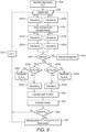
- the mixed-signal feedback loop is subdivided into three parts.
- the first part 400 comprises analogue pre-conditioning of the output voltages, including sampling and quantisation, by low-pass filter 405 and ADC 407 of each output.
- ADC 407 may be the appropriate one of ADCs 107, 108 of Figure 1 .
- the second part 410 relates to the "CCECSP" FSM 406 (corresponding to FSM 106), reading the ADC 407 outputs, performing calculations and determining actuating and control signals for the SIMO regulator.
- the third part 420 comprises a dead-time generator 425, followed by the switch drivers 430 and the switches 401 (corresponding to pairs of switches 101, 102).
- the resolution with which phase durations ta, tb, tc, and td are calculated is set to be at least lower than or equal to one-hundredth of the switching period ( T SW / 100 ) .
- clock multiplier mck is defined as a digital representation of the switching period T SW having a digital resolution of 128.
- the ADCs 407 have the main role to digitise the output voltages both in time and in amplitude.
- the sampling period i.e.
- Pre-conditioners for ADCs have a bandwidth BW of F sADC / 2 in order to avoid aliasing.
- the ADC sampling introduces a delay in Tsw within the chain.
- the number of bits of ADCs 407 determines the accuracy by which the SIMO can settle the outputs.
- the proposed "CCECSP" FSM 406 is able to control output voltages within 6*A RES accuracy.
- the total accumulated delay is a further parameter on which the SIMO system stability depends, and in this context it is limited to T SW +6*mck. Due to this unavoidable delay, the effective minimum time-slot for the charging and discharging phases is limited to 4*mck , i.e., the delay induced by the third part 420 of the chain.
- Figure 5 is a flow diagram showing steps of an exemplary algorithm of the algorithmic state machine (ASM) which implements the "start-up" state.
- the algorithm determines the phase durations ta, tb, tc, and td, and therefore the connected time duration for each output, in dependence only on the relationship between a first error voltage ve1 and a second error voltage ve2.
- First error voltage ve1 is calculated as the difference between the voltage vout1 at the first output 114 and a predetermined required voltage level vr1 for the output 114
- the second error voltage ve2 is calculated as the difference between the voltage vout2 at the second output 115 and a predetermined required voltage level vr2 for the output 115.
- step 510 updated data from the ADCs 107, 108 is received, comprising updated values for the output voltages vout1, vout2 and the supply voltage VDD.
- step 520 it is determined whether either one of error voltages ve1 and ve2 has become positive. If yes, "steady-state" state is entered and control transitions to the ASM of Figure 6 .
- This principle can be extended to arrangements with more than two outputs. In such a method error voltages from all the outputs are compared, and charging priority is assigned to the output having the highest absolute error voltage (the error voltages should all have negative values at start-up), with no priority assigned if all error voltages are equal. This process will end when at least one among outputs has reach its desired voltage (i.e., the error voltage goes positive).
- FIG. 6 is a flow diagram showing steps of an exemplary algorithm of the algorithmic state machine (ASM) which implements the "steady-state" state.
- ASM algorithmic state machine
- the initial priority output is set, such that one of the outputs is designated as a priority output P. This determines for which output the initial charging (or discharging) phase duration is first calculated. This concept is explained in more detail under the heading "Alternating the output Priority" below.
- step 602 updated data from the ADCs 107, 108 is received, comprising the most recently sampled values for the output voltages vout1, vout2 and the supply voltage VDD.
- the duration or length of first charging phase ta k may be calculated by an iterative update of duration ta k-1 , where discrete steps k correspond to a switching period Tsw.
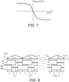
- This piece-wise linear error function is an approximation of error function f ⁇ ve 1 k ⁇ 1 vr 1 as shown in Figure 7 , this figure being a plot of both f ⁇ ve 1 k ⁇ 1 vr 1 (dotted line) and f pw ⁇ ve 1 k ⁇ 1 vr 1 (solid line) against ⁇ ve 1 k ⁇ 1 vr 1 .
- the error function shown is purely exemplary and its actual form is not critical to the concepts disclosed herein. As such, the error function may take a different form to that illustrated here.
- step 610 saturations (min and max) in the charging phase duration calculated in the previous step, here first charging phase duration ta k , are checked.
- the min saturation is imposed by technological constraints (it is the minimum required time to switch on and off pairs of switches 101, 102) whereas the max saturation is calculated to ensure there is sufficient time within the overall switching period for calculating and assigning the remaining time-slots.
- step 625 it is determined whether an interrupt has occurred: if so, interrupt management is performed at step 630 and the algorithm returns to step 602; if not it is determined at step 635a whether the sum of second charging phase duration tb k and second discharging phase duration tc k exceed the residual res. If so, at step 640a, second charging phase duration tb k and second discharging phase duration tc k are recalculated to fit the residual through the ratio slope2.
- This ratio ensures that no variation in charging and discharging for the second output occurs in the current switching period Tsw.
- Second discharging phase duration tc k is then recalculated according to Equation (4) with the recalculated tb k .
- a first calculation is performed (i.e., which output is designated as the priority output).
- a calculation is first performed for the connected time duration corresponding to the first output, specifically for the first charging period.
- steps 605a, 615a, 620a, 635a, 640a, 645a are substituted by steps 605b, 615b, 620b, 635b, 640b, 645b, as follows:
- the algorithm would be adapted where there are more than two outputs, to calculate charging and discharging phases for each output, and optionally to enable output priorities for the three or more outputs to be set and/or varied, such that each output may be designated as priority output.
- the order of calculation i.e., the designated priority output
- the charging phases may be calculated first (based on historical averages as described in the next section)
- the discharge phases may instead be calculated first in this manner.
- coefficients coeff1 and coeff2 are updated. These coefficients effectively increase the time resolution, and hence bandwidth, of the system as the magnitude of the error voltage at the corresponding output increases relative to the magnitude of an historical average of that error voltage.
- a respective error voltage moving average is used to update the coefficients coeff1 and coeff2 depending on the sign of the average errors.
- the coefficients in each step are updated by ⁇ 1, or else left unchanged.
- a sliding window is used on the last N error voltage readings (where N may be any integer; e.g, N may be between 1 and 20, between 1 and 10 and more specifically 4 or 8).
- the update process for coefficients coeff1 and coeff2 hence represent a superposition of a first-order infinite impulse response (IIR) filter with a non-linear function of low-pass finite impulse response (FIR) filter.
- IIR infinite impulse response
- FIR finite impulse response
- This combination is thus a non-linear time-variant filtering.
- the main effect off such non-linear time-variant filtering is to adapt the transient response to the error voltages ve1 and ve2, thereby improving stability: as an error voltage becomes greater in absolute value, the bandwidth of the system is increased enabling fast convergence of the system to a desired steady-state regime whereas a decrease of an error voltage translates into a progressive reduction in the bandwidth and consequent improvement in stability.
- the algorithm alternates for which output the charging phase (and consequently discharging phase) is first calculated. Periodically alternating the order with which the loads are connected to inductor further reduces cross-regulation of the two outputs.
- a first effect that this alternation of switching priority addresses is cross-regulation introduced by a systematic bias due to the order of calculation of the charging phases. By periodically changing priority, this bias is periodically switched to a different output.
- a second effect concerns the physical switching constraints and the sign of the spike which results from switching the output switches: by changing the priority to the other output, the sign of the spike is inverted.
- Figure 8 is a timing diagram of a steady state operation as described by Figure 6 .
- switching period T sw1 first output and second output are in steady state.
- switching period T sw2 the current at the first output is increasing with no change on the second output. Consequently, charging phase duration ta increases.
- the sum of phase durations tb and tc are lower than the residual, discharging phase duration td reduces.
- the sum of phase durations tb and tc will decrease slightly to reach a new steady state.
- a switching period T sw N ALT +1 i.e., the period immediately after N ALT cycles have passed. It can be seen that the priority in assigning the charging and discharging phases for the first and second outputs have been alternated, such that second charging phase duration tb is calculated first.
- priority output is switched between the outputs (e.g., rotated around the outputs), with the priority output being switched to a different output periodically, for example every N ALT switching periods.
- the switching between outputs may be in accordance with a predetermined order.
- priority output in this context refers (in the widest sense) only to the priority in the order of calculation of at least a first portion of its corresponding connected time duration. In a main embodiment, this first portion may be the corresponding charging phase, although it may instead be the corresponding discharging phase.
- SIDO regulators can occur when the difference between the load currents (the current ratio) at the two outputs is too high, e.g., when the current drawn at a first output is more than 30 times greater than the current drawn at the second output. In such a case the cross-regulation does not allow proper regulation of the second output voltage.
- digital logic may be added to detect a "locked" steady state condition followed by a determination as to whether the steady-state condition is valid or invalid.
- a stable counter may be employed and incremented each switching period T SW if the immediately previous M output voltage averages ve1 avg , ve2 avg at each output have presented no change, where M is any integer.
- integer M may be, for example, between 1 and 20, between 1 and 10 and more specifically 4 or 8. If the stable counter reaches a given threshold, the system is deemed to be in a "locked” condition. It is then determined whether the locked condition is a valid locked condition.
- a locked condition i.e., an invalid locked condition
- the corresponding output deemed to be at the incorrect voltage is fed by an LDO, leaving the other output connected as a (single output) step-down DC-DC regulator, or where there are more than two outputs, with the remaining outputs continuing to be connected and controlled as a SIDO/SIMO according to the methods described herein.
- CMOS transistors may be used to implement the ADCs and switches while the FSM and drivers may be implemented using digital cells. Hence it is a mixed-signal circuit.
- Phase durations ta, tb, tc and td may comprise non-overlapped phase durations to prevent charge sharing and charge loss between the nodes connected to the inductor.
- An advantage of implementing the FSM digitally is that it can be readily ported to other CMOS processes and, in addition, can be easily adapted to handle any number of outputs.
- switches and resistances are synonymous and should be understood to encompass situations where the connection or coupling is not direct (e.g., where there may be intervening elements or devices).
- switches and resistances are shown, it should be appreciated that this is purely by way of example and any suitable equivalent or similar devices may be used where it is possible to do so, or where there would be little effort for the skilled person to use such a suitable equivalent or similar device.
- the switches, resistances etc. may comprise any of, and where possible, any combination of: MOSFETs, LD-MOSFETS, other transistor devices or other switching devices.
Landscapes
- Engineering & Computer Science (AREA)
- Power Engineering (AREA)
- Physics & Mathematics (AREA)
- Electromagnetism (AREA)
- General Physics & Mathematics (AREA)
- Radar, Positioning & Navigation (AREA)
- Automation & Control Theory (AREA)
- Dc-Dc Converters (AREA)
Applications Claiming Priority (1)
| Application Number | Priority Date | Filing Date | Title |
|---|---|---|---|
| PCT/EP2016/082574 WO2018113996A1 (en) | 2016-12-23 | 2016-12-23 | Improvements in single inductor multiple output regulators |
Publications (2)
| Publication Number | Publication Date |
|---|---|
| EP3560085A1 EP3560085A1 (en) | 2019-10-30 |
| EP3560085B1 true EP3560085B1 (en) | 2024-11-06 |
Family
ID=57680276
Family Applications (1)
| Application Number | Title | Priority Date | Filing Date |
|---|---|---|---|
| EP16819575.8A Active EP3560085B1 (en) | 2016-12-23 | 2016-12-23 | Improvements in single inductor multiple output regulators |
Country Status (5)
| Country | Link |
|---|---|
| US (1) | US11038422B2 (enExample) |
| EP (1) | EP3560085B1 (enExample) |
| JP (1) | JP6980789B2 (enExample) |
| CN (1) | CN110100381B (enExample) |
| WO (1) | WO2018113996A1 (enExample) |
Families Citing this family (5)
| Publication number | Priority date | Publication date | Assignee | Title |
|---|---|---|---|---|
| EP3748833A1 (en) | 2019-06-04 | 2020-12-09 | Nxp B.V. | Single inductor dual output control method |
| US10924017B2 (en) * | 2019-06-13 | 2021-02-16 | Qualcomm Incorporated | Techniques for controlling a single-inductor multiple-output switched-mode power supply |
| US11703897B2 (en) * | 2020-03-05 | 2023-07-18 | Stmicroelectronics S.R.L. | LDO overshoot protection in a cascaded architecture |
| CN115395762B (zh) * | 2022-10-28 | 2023-03-24 | 深圳英集芯科技股份有限公司 | 单电感变压的多电压独立输出电路及相关产品 |
| CN117811335B (zh) * | 2023-12-29 | 2024-07-19 | 无锡中感微电子股份有限公司 | 低电压纹波的直流-直流转换器 |
Family Cites Families (23)
| Publication number | Priority date | Publication date | Assignee | Title |
|---|---|---|---|---|
| US6275016B1 (en) * | 2001-02-15 | 2001-08-14 | Texas Instruments Incorporated | Buck-boost switching regulator |
| US7249267B2 (en) * | 2002-12-21 | 2007-07-24 | Power-One, Inc. | Method and system for communicating filter compensation coefficients for a digital power control system |
| US7498690B2 (en) * | 2004-12-01 | 2009-03-03 | Texas Instruments Incorporated | System and method for regulating power in a multiple-output switching converter |
| US7759918B2 (en) * | 2006-06-16 | 2010-07-20 | Semiconductor Components Industries, L.L.C. | Method for inhibiting thermal run-away |
| US20080231115A1 (en) * | 2007-03-16 | 2008-09-25 | Gyuha Cho | Multiple-Output DC-DC Converter |
| WO2009152468A2 (en) * | 2008-06-13 | 2009-12-17 | The Regents Of The University Of Colorado, A Body Corporate | Monitoring and control of power converters |
| US8975879B2 (en) * | 2009-09-14 | 2015-03-10 | Dialog Semiconductor Gmbh | Switching converter having a plurality N of outputs providing N output signals and at least one inductor and method for controlling such a switching converter |
| US20110187189A1 (en) * | 2010-02-02 | 2011-08-04 | Intersil Americas Inc. | System and method for controlling single inductor dual output dc/dc converters |
| JP2012157145A (ja) * | 2011-01-26 | 2012-08-16 | Tbk:Kk | 双方向コンバータ、その制御回路およびその制御方法 |
| US9099919B2 (en) * | 2011-05-09 | 2015-08-04 | The Hong Kong University Of Science And Technology | Single-inductor-multiple-output regulator with synchronized current mode hysteretic control |
| JP5880239B2 (ja) * | 2012-04-13 | 2016-03-08 | 株式会社ソシオネクスト | 電源装置及び電源の制御方法 |
| JP5979955B2 (ja) * | 2012-04-20 | 2016-08-31 | ルネサスエレクトロニクス株式会社 | 半導体集積回路装置、電源装置及び電源装置の制御方法 |
| US9088211B2 (en) * | 2013-02-14 | 2015-07-21 | Texas Instruments Incorporated | Buck-boost converter with buck-boost transition switching control |
| TWI496405B (zh) * | 2013-07-05 | 2015-08-11 | Nat Univ Chung Cheng | A single inductance multi-stage output conversion device that increases the load range |
| CN107271756B (zh) * | 2014-12-04 | 2019-12-17 | 杰华特微电子(杭州)有限公司 | 负载电压检测电路及方法 |
| US9991793B2 (en) * | 2015-07-10 | 2018-06-05 | Kabushiki Kaisha Toshiba | Power supply circuit and control method for the same |
| CN105515376B (zh) * | 2015-12-31 | 2018-06-29 | 矽力杰半导体技术(杭州)有限公司 | 基于单电感多输出的电压调节电路及其控制方法 |
| KR101981212B1 (ko) * | 2016-01-11 | 2019-05-22 | 한국전자통신연구원 | 단일 인덕터 다중 출력 직류-직류 변환기, 그리고 그것의 동작 방법 |
| US9692296B1 (en) * | 2016-02-12 | 2017-06-27 | Texas Instruments Incorporated | Single-input-multiple-output (SIMO) DC-DC converters and SIMO DC-DC converter control circuits |
| CN105790582B (zh) * | 2016-03-08 | 2019-01-15 | 中山大学 | 一种单电感多输出直流-直流变换器及其控制方法 |
| JP2016106521A (ja) * | 2016-03-16 | 2016-06-16 | ルネサスエレクトロニクス株式会社 | デジタル制御電源装置 |
| US10622889B2 (en) * | 2016-08-24 | 2020-04-14 | Samsung Electronics Co., Ltd. | Voltage converting apparatus and method of controlling voltage converting apparatus |
| US10811982B2 (en) * | 2017-07-21 | 2020-10-20 | Solaredge Technologies Ltd. | Single inductor multiple output (SIMO) converter and control thereof |
-
2016
- 2016-12-23 WO PCT/EP2016/082574 patent/WO2018113996A1/en not_active Ceased
- 2016-12-23 CN CN201680091817.1A patent/CN110100381B/zh active Active
- 2016-12-23 US US16/472,853 patent/US11038422B2/en active Active
- 2016-12-23 JP JP2019534289A patent/JP6980789B2/ja active Active
- 2016-12-23 EP EP16819575.8A patent/EP3560085B1/en active Active
Also Published As
| Publication number | Publication date |
|---|---|
| CN110100381B (zh) | 2021-11-12 |
| WO2018113996A1 (en) | 2018-06-28 |
| US11038422B2 (en) | 2021-06-15 |
| US20190372464A1 (en) | 2019-12-05 |
| CN110100381A (zh) | 2019-08-06 |
| EP3560085A1 (en) | 2019-10-30 |
| JP2020502988A (ja) | 2020-01-23 |
| JP6980789B2 (ja) | 2021-12-15 |
Similar Documents
| Publication | Publication Date | Title |
|---|---|---|
| EP3560085B1 (en) | Improvements in single inductor multiple output regulators | |
| US8085024B2 (en) | Self-tuning digital current estimator for low-power switching converters | |
| US7570036B2 (en) | Multi-threshold multi-gain active transient response circuit and method for digital multiphase pulse width modulated regulators | |
| US8120203B2 (en) | Intelligent management of current sharing group | |
| EP1691474B1 (en) | Overcurrent protection for a buck-boost switching regulator | |
| US8138732B2 (en) | DCR sense for a COT power converter | |
| US20100060257A1 (en) | Current sensor for power conversion | |
| US9966832B1 (en) | Predictive ripple-cancelling signal into error amplifier of switch mode power supply | |
| US20180191333A1 (en) | Multi-phase control for pulse width modulation power converters | |
| US20160301313A1 (en) | Phase Current Estimation for Switching Power Converters | |
| US8575910B2 (en) | Single-cycle charge regulator for digital control | |
| US20180032096A1 (en) | Method and system for dc-dc voltage converters | |
| US10060954B2 (en) | Load capacitance determination circuitry and power supply control | |
| US20170141684A1 (en) | Method and System for DC-DC Voltage Converters | |
| US20190296641A1 (en) | Buck-boost switching converter | |
| US20190058400A1 (en) | Method and system for dc-dc voltage converters | |
| CN113783398A (zh) | 针对功率转换器的负载线调节 | |
| EP3823144A1 (en) | Method and apparatus for regulating an output voltage of a power converter during a load transient | |
| US10796830B1 (en) | Single inductor dual output control method | |
| CN112448578B (zh) | 开关电源电路 | |
| JP2013198253A (ja) | Dc/dcコンバータ | |
| Stack et al. | A high accuracy and high bandwidth current sense circuit for digitally controlled DC-DC buck converters | |
| US20250020700A1 (en) | Current sense circuit and current sensing method | |
| JP5272067B2 (ja) | スイッチング電源装置 | |
| Hashim et al. | Fast transient digitally controlled buck regulator with inductor current slew-rate boost |
Legal Events
| Date | Code | Title | Description |
|---|---|---|---|
| STAA | Information on the status of an ep patent application or granted ep patent |
Free format text: STATUS: UNKNOWN |
|
| STAA | Information on the status of an ep patent application or granted ep patent |
Free format text: STATUS: THE INTERNATIONAL PUBLICATION HAS BEEN MADE |
|
| PUAI | Public reference made under article 153(3) epc to a published international application that has entered the european phase |
Free format text: ORIGINAL CODE: 0009012 |
|
| STAA | Information on the status of an ep patent application or granted ep patent |
Free format text: STATUS: REQUEST FOR EXAMINATION WAS MADE |
|
| 17P | Request for examination filed |
Effective date: 20190718 |
|
| AK | Designated contracting states |
Kind code of ref document: A1 Designated state(s): AL AT BE BG CH CY CZ DE DK EE ES FI FR GB GR HR HU IE IS IT LI LT LU LV MC MK MT NL NO PL PT RO RS SE SI SK SM TR |
|
| AX | Request for extension of the european patent |
Extension state: BA ME |
|
| DAV | Request for validation of the european patent (deleted) | ||
| DAX | Request for extension of the european patent (deleted) | ||
| STAA | Information on the status of an ep patent application or granted ep patent |
Free format text: STATUS: EXAMINATION IS IN PROGRESS |
|
| 17Q | First examination report despatched |
Effective date: 20220215 |
|
| GRAP | Despatch of communication of intention to grant a patent |
Free format text: ORIGINAL CODE: EPIDOSNIGR1 |
|
| GRAP | Despatch of communication of intention to grant a patent |
Free format text: ORIGINAL CODE: EPIDOSNIGR1 |
|
| STAA | Information on the status of an ep patent application or granted ep patent |
Free format text: STATUS: GRANT OF PATENT IS INTENDED |
|
| INTG | Intention to grant announced |
Effective date: 20240614 |
|
| GRAS | Grant fee paid |
Free format text: ORIGINAL CODE: EPIDOSNIGR3 |
|
| GRAA | (expected) grant |
Free format text: ORIGINAL CODE: 0009210 |
|
| STAA | Information on the status of an ep patent application or granted ep patent |
Free format text: STATUS: THE PATENT HAS BEEN GRANTED |
|
| RAP3 | Party data changed (applicant data changed or rights of an application transferred) |
Owner name: U-BLOX AG |
|
| AK | Designated contracting states |
Kind code of ref document: B1 Designated state(s): AL AT BE BG CH CY CZ DE DK EE ES FI FR GB GR HR HU IE IS IT LI LT LU LV MC MK MT NL NO PL PT RO RS SE SI SK SM TR |
|
| REG | Reference to a national code |
Ref country code: GB Ref legal event code: FG4D |
|
| P01 | Opt-out of the competence of the unified patent court (upc) registered |
Free format text: CASE NUMBER: APP_54632/2024 Effective date: 20241003 |
|
| REG | Reference to a national code |
Ref country code: CH Ref legal event code: EP |
|
| REG | Reference to a national code |
Ref country code: DE Ref legal event code: R096 Ref document number: 602016090150 Country of ref document: DE |
|
| REG | Reference to a national code |
Ref country code: IE Ref legal event code: FG4D |
|
| PGFP | Annual fee paid to national office [announced via postgrant information from national office to epo] |
Ref country code: DE Payment date: 20241210 Year of fee payment: 9 |
|
| PGFP | Annual fee paid to national office [announced via postgrant information from national office to epo] |
Ref country code: GB Payment date: 20241226 Year of fee payment: 9 |
|
| PGFP | Annual fee paid to national office [announced via postgrant information from national office to epo] |
Ref country code: FR Payment date: 20241231 Year of fee payment: 9 |
|
| REG | Reference to a national code |
Ref country code: LT Ref legal event code: MG9D |
|
| REG | Reference to a national code |
Ref country code: NL Ref legal event code: MP Effective date: 20241106 |
|
| PG25 | Lapsed in a contracting state [announced via postgrant information from national office to epo] |
Ref country code: HR Free format text: LAPSE BECAUSE OF FAILURE TO SUBMIT A TRANSLATION OF THE DESCRIPTION OR TO PAY THE FEE WITHIN THE PRESCRIBED TIME-LIMIT Effective date: 20241106 Ref country code: PT Free format text: LAPSE BECAUSE OF FAILURE TO SUBMIT A TRANSLATION OF THE DESCRIPTION OR TO PAY THE FEE WITHIN THE PRESCRIBED TIME-LIMIT Effective date: 20250306 Ref country code: IS Free format text: LAPSE BECAUSE OF FAILURE TO SUBMIT A TRANSLATION OF THE DESCRIPTION OR TO PAY THE FEE WITHIN THE PRESCRIBED TIME-LIMIT Effective date: 20250306 |
|
| PG25 | Lapsed in a contracting state [announced via postgrant information from national office to epo] |
Ref country code: FI Free format text: LAPSE BECAUSE OF FAILURE TO SUBMIT A TRANSLATION OF THE DESCRIPTION OR TO PAY THE FEE WITHIN THE PRESCRIBED TIME-LIMIT Effective date: 20241106 Ref country code: NL Free format text: LAPSE BECAUSE OF FAILURE TO SUBMIT A TRANSLATION OF THE DESCRIPTION OR TO PAY THE FEE WITHIN THE PRESCRIBED TIME-LIMIT Effective date: 20241106 |
|
| REG | Reference to a national code |
Ref country code: AT Ref legal event code: MK05 Ref document number: 1740484 Country of ref document: AT Kind code of ref document: T Effective date: 20241106 |
|
| PG25 | Lapsed in a contracting state [announced via postgrant information from national office to epo] |
Ref country code: BG Free format text: LAPSE BECAUSE OF FAILURE TO SUBMIT A TRANSLATION OF THE DESCRIPTION OR TO PAY THE FEE WITHIN THE PRESCRIBED TIME-LIMIT Effective date: 20241106 |
|
| PG25 | Lapsed in a contracting state [announced via postgrant information from national office to epo] |
Ref country code: ES Free format text: LAPSE BECAUSE OF FAILURE TO SUBMIT A TRANSLATION OF THE DESCRIPTION OR TO PAY THE FEE WITHIN THE PRESCRIBED TIME-LIMIT Effective date: 20241106 |
|
| PG25 | Lapsed in a contracting state [announced via postgrant information from national office to epo] |
Ref country code: NO Free format text: LAPSE BECAUSE OF FAILURE TO SUBMIT A TRANSLATION OF THE DESCRIPTION OR TO PAY THE FEE WITHIN THE PRESCRIBED TIME-LIMIT Effective date: 20250206 |
|
| PG25 | Lapsed in a contracting state [announced via postgrant information from national office to epo] |
Ref country code: AT Free format text: LAPSE BECAUSE OF FAILURE TO SUBMIT A TRANSLATION OF THE DESCRIPTION OR TO PAY THE FEE WITHIN THE PRESCRIBED TIME-LIMIT Effective date: 20241106 Ref country code: LV Free format text: LAPSE BECAUSE OF FAILURE TO SUBMIT A TRANSLATION OF THE DESCRIPTION OR TO PAY THE FEE WITHIN THE PRESCRIBED TIME-LIMIT Effective date: 20241106 Ref country code: GR Free format text: LAPSE BECAUSE OF FAILURE TO SUBMIT A TRANSLATION OF THE DESCRIPTION OR TO PAY THE FEE WITHIN THE PRESCRIBED TIME-LIMIT Effective date: 20250207 |
|
| PG25 | Lapsed in a contracting state [announced via postgrant information from national office to epo] |
Ref country code: PL Free format text: LAPSE BECAUSE OF FAILURE TO SUBMIT A TRANSLATION OF THE DESCRIPTION OR TO PAY THE FEE WITHIN THE PRESCRIBED TIME-LIMIT Effective date: 20241106 |
|
| PG25 | Lapsed in a contracting state [announced via postgrant information from national office to epo] |
Ref country code: RS Free format text: LAPSE BECAUSE OF FAILURE TO SUBMIT A TRANSLATION OF THE DESCRIPTION OR TO PAY THE FEE WITHIN THE PRESCRIBED TIME-LIMIT Effective date: 20250206 |
|
| PG25 | Lapsed in a contracting state [announced via postgrant information from national office to epo] |
Ref country code: SM Free format text: LAPSE BECAUSE OF FAILURE TO SUBMIT A TRANSLATION OF THE DESCRIPTION OR TO PAY THE FEE WITHIN THE PRESCRIBED TIME-LIMIT Effective date: 20241106 |
|
| PG25 | Lapsed in a contracting state [announced via postgrant information from national office to epo] |
Ref country code: DK Free format text: LAPSE BECAUSE OF FAILURE TO SUBMIT A TRANSLATION OF THE DESCRIPTION OR TO PAY THE FEE WITHIN THE PRESCRIBED TIME-LIMIT Effective date: 20241106 |
|
| PG25 | Lapsed in a contracting state [announced via postgrant information from national office to epo] |
Ref country code: EE Free format text: LAPSE BECAUSE OF FAILURE TO SUBMIT A TRANSLATION OF THE DESCRIPTION OR TO PAY THE FEE WITHIN THE PRESCRIBED TIME-LIMIT Effective date: 20241106 |
|
| PG25 | Lapsed in a contracting state [announced via postgrant information from national office to epo] |
Ref country code: RO Free format text: LAPSE BECAUSE OF FAILURE TO SUBMIT A TRANSLATION OF THE DESCRIPTION OR TO PAY THE FEE WITHIN THE PRESCRIBED TIME-LIMIT Effective date: 20241106 |
|
| PG25 | Lapsed in a contracting state [announced via postgrant information from national office to epo] |
Ref country code: SK Free format text: LAPSE BECAUSE OF FAILURE TO SUBMIT A TRANSLATION OF THE DESCRIPTION OR TO PAY THE FEE WITHIN THE PRESCRIBED TIME-LIMIT Effective date: 20241106 |
|
| PG25 | Lapsed in a contracting state [announced via postgrant information from national office to epo] |
Ref country code: CZ Free format text: LAPSE BECAUSE OF FAILURE TO SUBMIT A TRANSLATION OF THE DESCRIPTION OR TO PAY THE FEE WITHIN THE PRESCRIBED TIME-LIMIT Effective date: 20241106 |
|
| PG25 | Lapsed in a contracting state [announced via postgrant information from national office to epo] |
Ref country code: IT Free format text: LAPSE BECAUSE OF FAILURE TO SUBMIT A TRANSLATION OF THE DESCRIPTION OR TO PAY THE FEE WITHIN THE PRESCRIBED TIME-LIMIT Effective date: 20241106 |
|
| REG | Reference to a national code |
Ref country code: CH Ref legal event code: PL |
|
| REG | Reference to a national code |
Ref country code: DE Ref legal event code: R097 Ref document number: 602016090150 Country of ref document: DE |
|
| PG25 | Lapsed in a contracting state [announced via postgrant information from national office to epo] |
Ref country code: LU Free format text: LAPSE BECAUSE OF NON-PAYMENT OF DUE FEES Effective date: 20241223 |
|
| PG25 | Lapsed in a contracting state [announced via postgrant information from national office to epo] |
Ref country code: SE Free format text: LAPSE BECAUSE OF FAILURE TO SUBMIT A TRANSLATION OF THE DESCRIPTION OR TO PAY THE FEE WITHIN THE PRESCRIBED TIME-LIMIT Effective date: 20241106 |
|
| PLBE | No opposition filed within time limit |
Free format text: ORIGINAL CODE: 0009261 |
|
| STAA | Information on the status of an ep patent application or granted ep patent |
Free format text: STATUS: NO OPPOSITION FILED WITHIN TIME LIMIT |
|
| PG25 | Lapsed in a contracting state [announced via postgrant information from national office to epo] |
Ref country code: MC Free format text: LAPSE BECAUSE OF FAILURE TO SUBMIT A TRANSLATION OF THE DESCRIPTION OR TO PAY THE FEE WITHIN THE PRESCRIBED TIME-LIMIT Effective date: 20241106 |
|
| REG | Reference to a national code |
Ref country code: BE Ref legal event code: MM Effective date: 20241231 |
|
| 26N | No opposition filed |
Effective date: 20250807 |
|
| PG25 | Lapsed in a contracting state [announced via postgrant information from national office to epo] |
Ref country code: BE Free format text: LAPSE BECAUSE OF NON-PAYMENT OF DUE FEES Effective date: 20241231 |
|
| PG25 | Lapsed in a contracting state [announced via postgrant information from national office to epo] |
Ref country code: CH Free format text: LAPSE BECAUSE OF NON-PAYMENT OF DUE FEES Effective date: 20241231 |
|
| PG25 | Lapsed in a contracting state [announced via postgrant information from national office to epo] |
Ref country code: IE Free format text: LAPSE BECAUSE OF NON-PAYMENT OF DUE FEES Effective date: 20241223 |