EP3557595A1 - Limitation d'un courant electrique de fonctionnement d'un circuit de courant de fonctionnement - Google Patents
Limitation d'un courant electrique de fonctionnement d'un circuit de courant de fonctionnement Download PDFInfo
- Publication number
- EP3557595A1 EP3557595A1 EP18167724.6A EP18167724A EP3557595A1 EP 3557595 A1 EP3557595 A1 EP 3557595A1 EP 18167724 A EP18167724 A EP 18167724A EP 3557595 A1 EP3557595 A1 EP 3557595A1
- Authority
- EP
- European Patent Office
- Prior art keywords
- winding
- electrical
- current
- limiting device
- conductor
- Prior art date
- Legal status (The legal status is an assumption and is not a legal conclusion. Google has not performed a legal analysis and makes no representation as to the accuracy of the status listed.)
- Withdrawn
Links
- 239000004020 conductor Substances 0.000 claims abstract description 151
- 238000004804 winding Methods 0.000 claims abstract description 134
- 230000000670 limiting effect Effects 0.000 claims abstract description 70
- 239000000463 material Substances 0.000 claims abstract description 45
- 230000005291 magnetic effect Effects 0.000 claims abstract description 29
- 238000001816 cooling Methods 0.000 claims abstract description 21
- 230000008878 coupling Effects 0.000 claims abstract description 19
- 238000010168 coupling process Methods 0.000 claims abstract description 19
- 238000005859 coupling reaction Methods 0.000 claims abstract description 19
- 238000004519 manufacturing process Methods 0.000 claims description 12
- 230000007704 transition Effects 0.000 claims description 12
- 238000000034 method Methods 0.000 claims description 10
- 230000000694 effects Effects 0.000 description 12
- 230000006870 function Effects 0.000 description 11
- 239000003302 ferromagnetic material Substances 0.000 description 10
- 230000001939 inductive effect Effects 0.000 description 8
- 230000002829 reductive effect Effects 0.000 description 8
- 238000011161 development Methods 0.000 description 7
- 230000018109 developmental process Effects 0.000 description 7
- 239000004065 semiconductor Substances 0.000 description 6
- 239000002887 superconductor Substances 0.000 description 6
- XEEYBQQBJWHFJM-UHFFFAOYSA-N Iron Chemical group [Fe] XEEYBQQBJWHFJM-UHFFFAOYSA-N 0.000 description 5
- PZKRHHZKOQZHIO-UHFFFAOYSA-N [B].[B].[Mg] Chemical compound [B].[B].[Mg] PZKRHHZKOQZHIO-UHFFFAOYSA-N 0.000 description 5
- 239000000758 substrate Substances 0.000 description 5
- XUIMIQQOPSSXEZ-UHFFFAOYSA-N Silicon Chemical compound [Si] XUIMIQQOPSSXEZ-UHFFFAOYSA-N 0.000 description 4
- 230000000712 assembly Effects 0.000 description 4
- 238000000429 assembly Methods 0.000 description 4
- 230000008901 benefit Effects 0.000 description 4
- 229910052710 silicon Inorganic materials 0.000 description 4
- 239000010703 silicon Substances 0.000 description 4
- 239000012809 cooling fluid Substances 0.000 description 3
- 230000001419 dependent effect Effects 0.000 description 3
- 238000013461 design Methods 0.000 description 3
- 238000010586 diagram Methods 0.000 description 3
- 238000005516 engineering process Methods 0.000 description 3
- 230000001976 improved effect Effects 0.000 description 3
- 229910000679 solder Inorganic materials 0.000 description 3
- 230000001960 triggered effect Effects 0.000 description 3
- 230000009471 action Effects 0.000 description 2
- 239000010949 copper Substances 0.000 description 2
- 230000002349 favourable effect Effects 0.000 description 2
- PCHJSUWPFVWCPO-UHFFFAOYSA-N gold Chemical compound [Au] PCHJSUWPFVWCPO-UHFFFAOYSA-N 0.000 description 2
- 229910052737 gold Inorganic materials 0.000 description 2
- 239000010931 gold Substances 0.000 description 2
- 230000007246 mechanism Effects 0.000 description 2
- 229910052574 oxide ceramic Inorganic materials 0.000 description 2
- 229910021521 yttrium barium copper oxide Inorganic materials 0.000 description 2
- 241000954177 Bangana ariza Species 0.000 description 1
- RYGMFSIKBFXOCR-UHFFFAOYSA-N Copper Chemical compound [Cu] RYGMFSIKBFXOCR-UHFFFAOYSA-N 0.000 description 1
- 229910000881 Cu alloy Inorganic materials 0.000 description 1
- 239000000853 adhesive Substances 0.000 description 1
- 230000001070 adhesive effect Effects 0.000 description 1
- 230000002411 adverse Effects 0.000 description 1
- 229910045601 alloy Inorganic materials 0.000 description 1
- 239000000956 alloy Substances 0.000 description 1
- 229910052782 aluminium Inorganic materials 0.000 description 1
- XAGFODPZIPBFFR-UHFFFAOYSA-N aluminium Chemical compound [Al] XAGFODPZIPBFFR-UHFFFAOYSA-N 0.000 description 1
- 238000013459 approach Methods 0.000 description 1
- 230000002238 attenuated effect Effects 0.000 description 1
- 230000015572 biosynthetic process Effects 0.000 description 1
- 230000008859 change Effects 0.000 description 1
- 238000010276 construction Methods 0.000 description 1
- 229910052802 copper Inorganic materials 0.000 description 1
- 238000013016 damping Methods 0.000 description 1
- 230000007423 decrease Effects 0.000 description 1
- 238000010292 electrical insulation Methods 0.000 description 1
- 238000005530 etching Methods 0.000 description 1
- 230000005496 eutectics Effects 0.000 description 1
- 230000005294 ferromagnetic effect Effects 0.000 description 1
- 230000005669 field effect Effects 0.000 description 1
- 239000011521 glass Substances 0.000 description 1
- 239000003292 glue Substances 0.000 description 1
- 230000006872 improvement Effects 0.000 description 1
- 230000006698 induction Effects 0.000 description 1
- 238000009434 installation Methods 0.000 description 1
- 239000011810 insulating material Substances 0.000 description 1
- 239000010410 layer Substances 0.000 description 1
- 238000001465 metallisation Methods 0.000 description 1
- 238000004377 microelectronic Methods 0.000 description 1
- 238000011017 operating method Methods 0.000 description 1
- 239000011224 oxide ceramic Substances 0.000 description 1
- 230000036961 partial effect Effects 0.000 description 1
- 230000008569 process Effects 0.000 description 1
- 238000012545 processing Methods 0.000 description 1
- 239000011241 protective layer Substances 0.000 description 1
- 230000007420 reactivation Effects 0.000 description 1
- 230000000717 retained effect Effects 0.000 description 1
- 238000000926 separation method Methods 0.000 description 1
- 229910052709 silver Inorganic materials 0.000 description 1
- 239000004332 silver Substances 0.000 description 1
- XLYOFNOQVPJJNP-UHFFFAOYSA-N water Substances O XLYOFNOQVPJJNP-UHFFFAOYSA-N 0.000 description 1
Images


Classifications
-
- H—ELECTRICITY
- H01—ELECTRIC ELEMENTS
- H01F—MAGNETS; INDUCTANCES; TRANSFORMERS; SELECTION OF MATERIALS FOR THEIR MAGNETIC PROPERTIES
- H01F38/00—Adaptations of transformers or inductances for specific applications or functions
- H01F38/02—Adaptations of transformers or inductances for specific applications or functions for non-linear operation
- H01F38/023—Adaptations of transformers or inductances for specific applications or functions for non-linear operation of inductances
-
- H—ELECTRICITY
- H01—ELECTRIC ELEMENTS
- H01F—MAGNETS; INDUCTANCES; TRANSFORMERS; SELECTION OF MATERIALS FOR THEIR MAGNETIC PROPERTIES
- H01F6/00—Superconducting magnets; Superconducting coils
-
- H—ELECTRICITY
- H01—ELECTRIC ELEMENTS
- H01F—MAGNETS; INDUCTANCES; TRANSFORMERS; SELECTION OF MATERIALS FOR THEIR MAGNETIC PROPERTIES
- H01F6/00—Superconducting magnets; Superconducting coils
- H01F2006/001—Constructive details of inductive current limiters
-
- H—ELECTRICITY
- H01—ELECTRIC ELEMENTS
- H01F—MAGNETS; INDUCTANCES; TRANSFORMERS; SELECTION OF MATERIALS FOR THEIR MAGNETIC PROPERTIES
- H01F6/00—Superconducting magnets; Superconducting coils
- H01F6/06—Coils, e.g. winding, insulating, terminating or casing arrangements therefor
- H01F6/065—Feed-through bushings, terminals and joints
Definitions
- the invention relates to a current limiting device for limiting an electrical operating current of an operating circuit having a first and a second electrical connection for connection to the operating circuit, a first winding having at least a first electrical conductor, wherein in each case a conductor end of the at least one first electrical conductor to a a second winding having at least a second electrical conductor made of an electrically superconducting material whose conductor ends are electrically coupled to each other, wherein the first and the second winding are arranged to make a magnetic coupling, and a cooling unit, the is designed to cool the second winding in normal operation to a temperature which is less than a transition temperature of the electrically superconducting material.
- the invention further relates to a method for operating a current limiting device for limiting an electrical operating current of an operating circuit, wherein a first winding, which has at least one first electrical conductor and is connected to the operating circuit, is acted upon by an electrical operating current of the operating circuit, a second winding with at least one second electrical conductor made of an electrically superconducting material whose conductor ends are electrically coupled to each other, is magnetically coupled to the first winding, and the second winding is cooled during normal operation to a temperature which is less than a transition temperature of the electrically superconducting material ,
- the invention also relates to a method for producing a current limiting device for limiting an electrical operating current of an operating circuit, wherein a first winding with at least a first electrical conductor is made, wherein in each case a conductor end of the at least one first electrical conductor is connected to a respective one of two electrical terminals for connecting the current limiting device to the operating circuit, a second winding is produced with at least one second electrical
- Generic current limiting devices also called superconducting current limiters (SFCL) for short, are well-studied devices which are suitable for limiting operating currents outside normal operation, in particular for an overcurrent which is greater than a rated current, such as, for example, in the event of a short circuit in an electrical center. or high-voltage system, serve. They can be designed with different concepts both as predominantly inductive and as predominantly resistive current-limiting devices or also from any combination of both concepts.
- SFCL superconducting current limiters
- Resistive current limiting devices are electrically connected directly to the operating circuit.
- a resistive current-limiting device generally has a superconducting band conductor, which is acted upon by the operating current of the operating circuit.
- inductive current limiting device two different concepts are in use, on the one hand with a shielded ferromagnetic material and on the other hand with a premagnetized ferromagnetic material.
- a current is induced by means of an electrical coil through which the operating current flows due to a magnetic coupling in a superconducting winding.
- the ferromagnetic material is shielded and temporarily ineffective.
- the ferromagnetic material is effective and there is a change in the impedance, which acts to limit the current.
- An electric voltage which drops in the case of engagement of the limiting means at the current limiting means can be adjusted via a turns ratio of the first and second windings and via the resistive resistance of the superconducting winding in the non-superconducting state.
- the current-limiting device can conduct an overcurrent, for example the short-circuit current, for a given time, for example a few seconds.
- an overcurrent for example the short-circuit current
- An important condition for the use of a generic current-limiting device is further that, especially in the case of short circuit, the current in the superconductor is rapidly interrupted.
- interruption of the current in the superconductor is possible only by switching off the current through the choke coil. Decisive here is therefore the switching off of the current in the superconductor. If possible, the current-limiting functionality should be retained.
- a heated superconducting material to produce its superconducting electrical conductivity may need to be cooled below the transition temperature again, so that the superconducting current flow, which is in the normal operation of the current limiting device, when the operating current is smaller than the reference current can be resumed.
- a period of several seconds may be required for appropriate cooling. This applies to the frequently used above-mentioned concepts both for the resistive current-limiting device and for the inductive current-limiting device with the shielded ferromagnetic material.
- Current limiting devices are generally used in power engineering, in particular the electrical power supply.
- electrical power engineering such current limiting devices are used using choke coils according to the principle of the shielded iron core (shielded, ferromagnetic material) or the Gleichstromvormagnetinstrumenten iron core (pre-magnetized ferromagnetic material).
- the iron cores used there have a high volume and a high weight and incidentally in normal operation outside the current limiting functionality a comparatively high impedance with respect to the operating circuit to which they are connected cause.
- a generic current limiting device discloses, for example, the DE 10 2007 007 087 A1 US-A-4/51325 discloses a current limiting device having a variable coil impedance.
- a superconducting coil inside a choke coil, the inductance and consequently also the impedance of the choke coil can be reduced. This is done by inducing a current in the superconducting coil through the choke coil which at least partially compensates for a magnetic field of the choke coil.
- the superconducting coil is cooled by means of a cryostat to a temperature which is lower than the transition temperature of the particular superconducting material used. This coil is shorted.
- the superconducting coil at least partially compensates the magnetic field of the choke coil.
- the inductance of the choke coil is reduced and a voltage drop across the choke coil is reduced accordingly.
- the current limiting functionality is realized in that at a certain current value of the operating current, which is applied to the choke coil and which is greater than the comparison value, the superconducting material of the superconducting coil is in a normal state.
- the inductance of the choke coil as a whole increases, so that thereby a current limiting functionality of the choke coil can be achieved.
- the current limiting device is therefore formed here from a choke coil which is magnetically coupled to the superconducting coil.
- the current-limiting device basically does not need any ferromagnetic material, in particular also no iron core.
- the above procedure is also applicable to an inductive current limiting device based on the principle of the shielded iron core.
- the current limiting effect is usually lower than in the case of a resistive current-limiting device, it is customary to use a parallel-connected choke coil waived.
- it is not easily possible to interrupt the electric current flowing through the second winding because the electric current in the second winding is induced solely by magnetic coupling with the first winding. For this reason, therefore, usually the first winding is switched off from the operating circuit and thus interrupted the operating current.
- an inductive current limiter for DC applications is known, which is designed as an inductive superconducting current limiter, also known as Superconducting Fault Current Limiter (SFCL), and whose function is based on a magnetic field of a flow-rate reactor by means of a short coil of a superconducting material compensate to provide the lowest possible inductance through the inductor outside the limiting functionality.
- SFCL Superconducting Fault Current Limiter
- the superconducting coil can no longer conduct the corresponding coil current superconducting, whereby the compensation of the magnetic field is significantly reduced.
- the inductance of the inductor increases accordingly strong.
- the superconducting coil may initially be cooled below the critical temperature again due to thermal effects during the triggered state.
- the resistive solder joint has the disadvantage of limited effectiveness.
- the time to restore the normal operating state outside the triggered state is comparatively long.
- the invention has for its object to improve reactivation of the current limiting device after triggering due to an operating current that is greater than the comparison current to improve.
- the invention proposes a current-limiting device, a method for operating the current-limiting device and also a method for producing the current-limiting device according to the independent claims.
- a generic current-limiting device it is in particular proposed that it has a switching unit for electrically coupling the conductor ends of the at least one second electrical conductor as a function of a switching state of the switching unit.
- the conductor ends of the at least one second electrical conductor are electrically coupled as a function of a switching state of a switching unit coupling the conductor ends.
- a switching unit is arranged, by means of which the conductor ends of the at least one second electrical conductor are electrically coupled as a function of a switching state of the switching unit.
- the invention is based on the idea that by integrating a switching unit in the current limiting device a shutdown for a current flow in the second winding can be achieved so that the adverse effects caused by the triggering of the current limiting device, can be returned quickly and quickly. As a result, proper operation of the current-limiting device can be achieved again as soon as possible.
- the switching unit may comprise one or more electromechanical switching elements and optionally also semiconductor switches as needed. Of course, combinations thereof may be provided.
- the switching unit is arranged directly in the region of the second winding and, moreover, can also be formed in one piece with the second winding. This allows a compact design can be achieved, so that the intended functionality of the current limiting device can be improved.
- the operating circuit is a circuit in which a predetermined operating current flows during normal operation in an undisturbed state. This stream can preferably be performed permanently in the operating circuit.
- the operating circuit can thus be, for example, an electrical energy supply network, in particular a medium-voltage network or a high-voltage network.
- the invention is not limited to medium voltage or high voltage applications. Of course, it can also be used at a low voltage, in particular a low voltage according to the Directive 2014/35 / EU of the European Parliament and of the Council of 26 February 2014 on the harmonization of the laws of the Member States relating to the supply of electrical equipment for use within certain voltage limits in the market.
- Low voltage means in particular an alternating voltage between about 50 V and 1000 V or a DC voltage between about 75 V and about 1500 V.
- Mean voltage means in particular an electrical AC voltage between about 1000 V to about 52 kV.
- High voltage means in particular an alternating voltage that is greater than about 52 kV, in particular greater than 60 kV, preferably greater than 63
- the operating circuit is used to electrically couple electrical devices such as electrical loads, electrical power generators and / or the like for the purpose of exchanging electrical energy.
- the operating current is therefore an electrical current which serves to distribute the electrical energy between the electrical devices connected to the operating circuit.
- the current limiting device preferably has the first and the second electrical connection for connection to the operating circuit.
- the current-limiting device is therefore designed, in particular, to be connected to the operating circuit in such a way that the operating current of the operating circuit also flows through the current-limiting device. This purpose is served by the first and the second electrical connection.
- the current-limiting device can therefore have its own housing as an individually manageable module, on which the two electrical connections are arranged in order to enable a connection to the operating circuit.
- appropriate electromechanical connection means such as plug and / or screw terminals, solder joints, clamp connections and / or the like may be provided.
- the current-limiting device has the first winding, which has at least one electrical conductor, wherein in each case one conductor end of the at least one first electrical conductor is connected to a respective one of the electrical connections. If two or even more first electrical conductors are provided, these are preferably connected in parallel to the terminals.
- the plurality of first electrical conductors are preferably also arranged spatially substantially parallel.
- the first winding can thus provide a choke coil, which provides an electrical inductance in a known manner.
- the first winding has at least a single turn of the at least one first electrical conductor. As a rule, however, a plurality of turns of the at least one electrical conductor are provided for forming the first winding.
- the first electrical conductor may be an ordinary electrical conductor, which may have a variety of cross-sectional shapes such as round, square, combinations thereof and / or the like as needed. Also conceivable are waveguides, for example tubes, for cooling, for example by means of water. This could be particularly interesting in this concept, due to the advantageous compact design, in particular with respect to a magnetic coupling between the first and the second winding.
- the electrical conductor may preferably have an insulating layer, so that, in particular in the case of a plurality of adjacently arranged turns, an electrical insulation can be achieved with respect to adjacently arranged turns or by means of further first electrical conductors.
- the at least one first electrical conductor may be formed from a material such as copper, aluminum, alloys thereof and / or the like.
- a conductor cross section of the first electrical conductor is preferably adapted to a rated current for the operating circuit.
- the conductor ends are preferably connected directly to the first and the second electrical connection.
- the current-limiting device furthermore has the second winding with the at least one second electrical conductor made of an electrically superconducting material.
- the electrically superconducting material may be, for example, YBCO or the like. But other suitable materials that show superconducting properties can be used here. Combinations thereof may also be provided.
- the at least one second electrical conductor may, like the first electrical conductor, have a suitable cross-section in order to achieve the desired current conduction during normal operation to realize in the second winding. Even if a shape of the cross section of the at least one second electrical conductor can be selected as well as the at least one first electrically conductor, the second electrical conductor is preferably designed as a strip.
- the shape of the cross sections of the at least one first and the at least one second conductor may be selected to be approximately equal and also different from each other.
- the second electrical conductor likewise has conductor ends, which, however, are electrically coupled to one another here, unlike the at least one first electrical conductor, so that the second winding can be substantially short-circuited.
- the first and second windings are arranged to make a magnetic coupling with each other. This makes it possible for the first and the second winding to interact magnetically with one another. If the first winding flows through the operating current, it generates a magnetic field, which causes a corresponding current flow in the second winding. Since the second winding can be substantially short-circuited by the coupling of the line ends of the second electrical conductor, a compensation of the magnetic field generated by the first winding can be achieved hereby. An inductance of the first winding can thereby be reduced.
- the compensation of the inductance can be achieved particularly favorable in that the superconducting material is cooled by means of the cooling unit to a temperature which is less than its transition temperature.
- the second winding is superconducting if it is correspondingly cold.
- a large compensation effect with respect to the inductance of the first winding can be achieved.
- the operating current is smaller than the comparison value, which may correspond to a comparison current, thus an almost complete compensation of the inductance of the first winding can be achieved, especially if the second Winding is arranged and / or aligned within the first winding.
- the current flow in the second winding increases in such a way that the superconducting effect of the at least one second electrical conductor is reduced or even completely lost. Consequently, as a result, the inductance of the first winding increases, so that the current limiting device provides a large inductance in order to achieve the desired current limiting function can.
- the current-limiting device hardly affects the operating circuit. If, however, the operating current is greater than the comparison current, the inductance increases, preferably almost directly, so that the desired current-limiting effect can be provided.
- the comparison value which is dependent on properties of the second winding, thus determines from which current the current limiting device provides its current limiting functionality. As a result, the comparison value or the comparison current can be determined.
- the cooling unit can be designed, for example, as an integrated cryostat or the like.
- the cooling unit can of course also be formed only by a suitable heat exchanger device, which is connected to a corresponding heat sink.
- the cooling unit is preferably thermally well coupled to the second winding, in particular the second electrical conductor.
- the switching unit is provided according to the invention.
- the switching unit namely the conductor ends the at least one second electrical conductor are electrically separated from each other depending on the switching state of the switching unit.
- a current flow in the second electrical conductor can be interrupted so that the standby mode of the current-limiting device can be restored almost in a timely manner.
- disconnecting the initial state does not need to be restored immediately. After disconnecting, it is possible to wait for a re-cooling time, before subsequently switching the switching unit back into the switched-on switching state. Then the initial state is restored.
- one or more electromechanical switching elements and also alternatively or additionally semiconductor switching elements can be provided.
- the switching element or the switching elements can be arranged integrated into the second winding.
- a separate control unit is provided, by means of which the switching unit is controlled in the desired manner.
- the switching unit may preferably occupy at least two switching states, namely a switched-on switching state and a switched-off switching state. In the switched-on switching state, the conductor ends of the second electrical conductor are directly electrically connected to each other. In the switched-off state, the conductor ends, however, are electrically isolated from each other, so that a current flow can be substantially interrupted.
- the winding namely the first and / or the second winding, is preferably formed from the at least one electrical conductor, which provides at least one turn for this winding.
- a plurality of conductors may be provided, which are preferably arranged adjacent to each other and which may be connected in series and / or also connected in parallel.
- the second winding can Furthermore, it can be provided that, in the case of a plurality of electrical conductors, the respective electrical conductors can be short-circuited by means of the switching unit.
- the switching unit can provide appropriate switching elements for this purpose.
- the operating current can be lowered and thereby adapted to the requirements of the energy supply network.
- the switching unit is also thermally coupled to the second winding. It can thereby be achieved that a thermal gradient within the second winding can be largely avoided. In particular, in standby mode, an expense for the cooling of the second conductor can therefore be kept as low as possible.
- the thermal coupling of the switching unit can be achieved, for example, in that the switching unit is formed integrally with the second winding.
- the conductor ends of the at least one electrical conductor of the second winding are preferably arranged opposite one another and the switching unit is designed to produce the electrical coupling of the line ends by means of at least one contact bridge.
- the conductor ends can be electrically coupled to one another in a simple manner, without the conductor ends having to be mechanically moved or actuated. Especially with superconducting materials, which often have mechanically unfavorable properties, this is advantageous. Thereby, a reliable switching unit can be provided.
- the switching unit comprises a microswitch arrangement with a plurality of microswitches.
- the micro switch arrangement it is possible to integrate the switching unit in a simple manner, in particular in the second winding.
- the micro-switch assembly may be in the manner of a micro-electro-mechanical system Be formed (MEMS).
- MEMS micro-electro-mechanical system Be formed
- the microswitches may in particular be formed by electromechanical switching elements and, for example, have dimensions in the range from about 10 ⁇ m to about 100 ⁇ m or more.
- the microswitches can be manufactured by manufacturing processes of semiconductor technology, for example by using etching or the like.
- the microswitches can be directly connected to the at least one second electrical conductor, in particular on the superconducting material or its protective layer, which may preferably consist of silver of gold, of the at least one second conductor.
- microswitch can have the further advantage that a light resistive electrical resistance can thereby be created, in particular in standby mode, which can be advantageously used for reducing the current in the second winding.
- a light resistive electrical resistance can thereby be created, in particular in standby mode, which can be advantageously used for reducing the current in the second winding.
- the switching elements in particular the micro-switches, can be designed to be actuated, for example, electrostatically, electromagnetically, electrothermomechanically or even piezoelectrically or the like.
- These drive mechanisms for the switching elements or the microswitches preferably do not require any direct mechanical contact in order to be able to actuate the switching element or the microswitch. This is particularly advantageous in view of the fact that the switching elements or the micro-switch can be arranged integrated into the second winding. Since the second winding, in particular the second electrical conductor, must be cooled as a rule, this can easily control the Switching elements or the microswitch be realized outside a cooled area.
- the switching elements or the microswitches are designed substantially insensitive to a magnetic action, so that the functionality can be largely avoided by a possible magnetic field of the first winding.
- the switching elements or the microswitches could also be arranged within the second winding, in which case they would then be arranged in the standby mode in a magnetically shielded region, it should be borne in mind that if the comparison current is exceeded by the operating current, the superconducting effect of the material is lost or can be attenuated, whereby a shielding effect is reduced accordingly or eliminated and the switching elements or the microswitch would then be exposed to the magnetic field.
- the microswitches are at least partially connected in parallel. This makes it possible to use standardized microswitches and to connect them in parallel as required in order to be able to carry out a predefinable rated current in the switched-on switching state. This proves to be particularly advantageous when a plurality of standardized micro-switches is arranged on a common carrier. As a result, the parallel connection can also be realized in a simple way, which can be achieved at least partially via the carrier.
- microswitches are at least partially connected in series.
- This development has the advantage that an improved dielectric strength can be achieved. Since only relatively small creepage and clearance distances can usually be realized by means of the microswitch, it may be useful to achieve a predetermined dielectric strength, a suitable number of micro-switches to connect in series. As a result, the requirements in terms of creepage distances and clearances can be better met.
- this development may also include an at least partial parallel connection of the microswitch.
- the microswitches can be manufactured in a simple manner using known semiconductor technology manufacturing methods.
- it can be achieved in this way that the micro-switches can be formed with substantially the same electrical and / or mechanical properties, so that reliable operation of the individual micro-switches can be achieved with low tolerances.
- a simple arrangement of the microswitch arrangement in the region of the second winding can be achieved in this way.
- the microswitch arrangement is designed to control at least some of the microswitches by means of a common control signal. As a result, a uniform actuation of the individual microswitches can be achieved. This proves to be particularly advantageous when some of the microswitches are connected in parallel or also connected in series. Overall, so that a reliable switching operation can be achieved.
- the microswitches have a respective pivoting lever whose pivotal state is adjustable by means of a drive element at least as a function of the switching state of the switching unit.
- a suitable contact element can be arranged on the pivot lever, which can contact an opposite contact element or also a plurality of contact elements, which are preferably stationarily positioned, in a respective pivot position.
- the pivot state of the pivot lever can be adjusted accordingly by means of the drive element, so that the desired Switching state of the switching unit can be made.
- the drive element or the drive unit can be formed by a contact, which acts on the pivoting lever via a force field in order to be able to pivot it into the desired pivoting position which corresponds to the respective switching state.
- each swivel lever of the micro-switch is assigned its own drive element, wherein the micro-switch arrangement is designed to control the drive elements independently of each other.
- the micro-switch arrangement is designed to control the drive elements independently of each other.
- the current distribution of the microswitches can be set in parallel operation by the action of a respective force of the drive element on the pivoting lever.
- corresponding spring elements can be provided in addition, by means of which the force can be calibrated appropriately.
- the drive elements are independently controllable, so that, if necessary, the current control of the individual micro-switches can be varied almost individually.
- the microswitches are magnetically unaffected. It can thereby be achieved that the functionality of the microswitch is not influenced by a magnetic field of the first and / or the second winding. This can be accomplished by selecting one or more suitable materials for the microswitches, which are preferably non-ferromagnetic.
- the second winding comprises at least two electrical conductors formed separately from one another and the switching unit is designed to couple the respective conductor ends of these electrical conductors separately depending on the switching state of the switching unit.
- the at least two second electrical conductors can be operated almost independently of each other.
- they are electrically insulated from each other. This makes it possible to adjust the functionality of the second winding as needed.
- the switching unit is designed to provide mutually independent respective switching states for the second electrical conductors. This makes it possible to adjust the current limiting device not only during commissioning, but also during normal operation later. As a result, a highly flexible current-limiting device can be achieved.
- the production of micro-switches can be at least partially comparable to the manufacturing process of the second electrical conductor of the superconducting material.
- the microswitch directly, preferably directly, on or in the superconducting second conductor, in particular to integrate.
- the at least one second electrical conductor is designed as a band conductor.
- the at least one second electrical conductor in particular in turns thereof.
- This can be achieved in that the at least one second electrical conductor forms only a single turn of the second winding.
- a plurality of second electrical conductors may be provided which form respective further individual turns. Each of these windings can be equipped correspondingly switchable by means of a microswitch arrangement.
- a switching unit in particular a micro switch arrangement
- a winding of at least one second electrical conductor made of a superconducting material on the one hand good damping of the current of the second winding can be achieved.
- the at least one second electrical conductor can be switched off without having to separate the first winding, which is connected in the operating circuit in the manner of a choke coil, from the operating circuit.
- the switching unit in particular the microswitch assembly
- a galvanic separation of the corresponding conductor ends can be achieved.
- the switching unit in particular the microswitch arrangement, makes it possible to achieve a very short turn-off time, for example of a few microseconds or the like. Since a small induced voltage can be achieved by a suitable construction with preferably a few turns, problems when switching off the second winding by means of the switching unit arcs can be largely avoided.
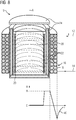
- FIG. 8 shows a schematic sectional view of a current limiting device 10 for limiting an electrical operating current of an operating circuit not shown.
- the current limiting device 10 has a first and a second electrical connection 12, 14 for connection to the operating circuit. This is in FIG. 8 only shown schematically.
- the current limiting device 10 comprises a first winding 16 in the manner of a choke coil, which has a first electrical conductor 18 made of a copper alloy, which forms the first winding 16 with a plurality of turns.
- the first winding 16 is formed in the manner of a cylindrical coil. Conductor ends of the first electrical conductor 18 are connected to a respective one of the electrical terminals 12, 14. As a result, the first winding 16 can be acted upon by the operating current of the operating circuit.
- the current-limiting device 10 furthermore comprises a second winding 20 with a plurality of second electrical conductors 22 made of an electrically superconducting material, in the present case magnesium diboride.
- an electrically superconducting material in the present case magnesium diboride.
- Magnesium diboride has a transition temperature of about 39 K and thus applies as a high-temperature superconductor, but other superconducting materials are known, which have higher transition temperatures.
- the superconducting material may also comprise an oxide ceramic material as a high-temperature superconductor.
- this may be a material of the type REBa 2 Cu 3 O x .
- This material class advantageously allows the formation of electrical conductors with high transition temperatures, in particular with respect to the critical temperature of magnesium diboride.
- the application of the invention is not limited to these materials.
- other suitable superconducting materials can also be used.
- YBCO ReBCO
- ReBCO is particularly suitable as a superconducting material which can be used as an alternative to magnesium diboride.
- each of the second electrical conductors 22 forms a single winding of its own, wherein the respective conductor ends of a respective one of the second electrical conductors 22 are electrically coupled together.
- each of the second electrical conductors 22 forms a short-circuited turn of the second winding 20.
- the individual windings are arranged coaxially adjacent to one another, so that in this case too a coil essentially in the form of a cylindrical coil is formed.
- the first and second windings 16, 20 are arranged to make a magnetic coupling.
- the first and the second winding each of which is substantially cylindrically shaped, are arranged to each other such that the second winding 20 within an inner diameter of the first winding 16 concentric with the first winding 16 with respect to an axis A is arranged.
- the first and the second winding in the present case have approximately the same axial extent.
- the turns of the second electrical conductors 22 form short-circuited individual turns.
- the first and second windings 16, 20 are thus magnetically coupled.
- a cooling unit 24 which comprises a container made of a thermally insulating material and a in the Has substantially cylindrical cup shape, which can be formed closed at a first end and closed at a second end by means of a circular disc.
- the second winding 20 is arranged inside the container of the cooling unit 24.
- the container is arranged together with the second winding 20 within the inner diameter of the first winding 16.
- a cooling fluid 38 is further arranged, by means of which the second winding 20 can be cooled to a lower temperature than the transition temperature of the superconducting material of the second electrical conductor 22.
- the container of the cooling unit 24 is formed of a non-ferromagnetic material.
- FIG. 8 is a schematic diagram representation provided, from which a course of a magnetic field strength is shown as a function of a radius with respect to the axis A. Below a predetermined comparison current, in which the second winding 20 carries a current in the superconducting operating state, a magnetic field strength H within the second winding 20 is approximately zero. In a region between the inner radius and an outer radius of the second winding 20, the magnetic field strength H increases up to a maximum value of H 1 .
- This value of the magnetic field strength remains substantially constant up to the inner diameter of the first winding 16. In the further course radially outward then decreases the magnetic field strength H in a known manner until it reaches a minimum value, to then approach outside of the first winding 16 with increasing radius zero.
- the field strength curve of the magnetic field strength is shown schematically as a function of the radial distance from the axis A.
- the current limiting device 10 In the in FIG. 8 In the illustrated state, the current limiting device 10 is in a standby mode, which is maintained as long as the operating current is less than the comparison current.
- the comparison current is greater than the comparison value
- the second winding 20, in particular its second electrical conductor 22 leaves the superconducting state and the field strength course changes to the effect that a magnetic field now also occurs within the second winding 20.
- the inductance of the first winding 16 correspondingly increases, whereby the current limiting device 10 provides a high impedance with respect to the operating current.
- the operating current if it is greater than the comparison value, be limited.
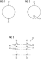
- FIG. 1 and FIG. 9 now show a first embodiment for the second winding 20 according to the invention.
- a schematic plan view of the second winding 20 is shown.
- an associated schematic side view of the winding 20 is shown.
- the conductor ends of the second electrical conductors 22 are electrically connected to respective micro switch assemblies 26 as switching units.
- the respective second electrical conductor 22 can either be short-circuited or opened.
- the second electrical conductors 22 are presently designed as a band conductor and the micro switch assemblies 26 are attached to the respective conductor ends.
- FIG. 2 and FIG. 10 show an alternative embodiment of the second winding 20, wherein the conductor ends of the second electrical conductors 22 are bent inwardly and the micro switch assemblies 26 attached to the inner conductor ends are.
- the microswitch assemblies 26 are substantially protected against magnetic field in a standby mode of the current limiting device 10, wherein the operating current is smaller than the comparison current. This is also particularly advantageous if switches other than MEMS are used.
- FIG. 3 shows a schematic diagram representation of a microswitch assembly 26, as in the previous embodiments according to the 1 and 2 respectively 9 and 10 can be used. It can be seen that a plurality of microswitches 30 mounted on a common carrier 32 (FIG. FIG. 4 ) are arranged in series, in order to provide a predetermined dielectric strength in the off state can. In order at the same time to be able to achieve a corresponding current-carrying capacity in the switched-on state, several of the aforementioned series circuits are connected in parallel. By the number of series-connected and / or parallel microswitch 30, a rated current and also a rated voltage can be adjusted if necessary.
- the second electrical conductors 22 are band-shaped and have a width of about 12 mm.
- a thickness of the band-shaped second conductor 22 is about 0.15 mm. Due to the special design of the second winding 20 can be achieved that when opening the micro-switch assembly 26 only a voltage of some 10 V is applied, although the current limiting device 10 can be operated in an operating circuit, which is designed for a rated voltage of about 10 kV or more ,
- the number of parallel connected series circuits of microswitches 30 may be selected depending on the rated current, which may be, for example, in a range of about 100 A to about 1 kA or more.
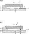
- FIG. 4 shows a schematic sectional view of a single microswitch 30 of the microswitch assembly 26. It can be seen that the micro-switch 30 is disposed on a substrate 32 and the carrier. Although only a single microswitch is shown in the present case, it is provided in the present embodiment that all of the microswitches 30 are in accordance with FIG FIG. 3 are arranged on the common substrate 32.
- the substrate 32 is formed of glass. However, another suitable material may be chosen.
- the substrate 32 is connected to a silicon plate 50 by means of a eutectic adhesive 48, wherein the silicon plate 50 and the substrate 32 are treated accordingly by known methods to form a pivoting lever 34 of the respective microswitch 30.
- the pivot lever 34 is elastic due to its dimensions and can therefore be used to realize a switching function of the microswitch 30.
- the pivot lever 34 is fixedly arranged for this purpose with a first end 52, so that a second end 54 is pivotable in a predetermined manner.
- a contact bridge 28 is arranged, which is fixedly connected to the second end 54 of the pivot lever 34.
- the contact bridge 28 has an electrically conductive connecting element 46.
- connecting element 46 electrical contact elements 42, 44 are arranged on the corresponding conductor ends of the second electrical conductor 22.
- an electrical contact between the contact elements 42, 44 is produced by means of the connecting element 46 of the contact bridge 28.
- the contact bridge 28 with the connecting element 46 is arranged away from the contact elements 42, 44, so that a current through the respective one of the second electrical conductors 22 is suppressed. This can be seen in the perspective Representation of a section of the microswitch 30 in the schematic representation according to FIG. 5 ,
- a contact stroke in the present case about 2 microns to about 3 microns.
- a length of the pivot lever 34 is presently about 200 microns to about 300 microns.
- an electrostatic drive element 36 is presently provided.
- the drive element 36 comprises a metallization as an electrode, which can be acted upon by means of a control device, not shown, with a predetermined electrical voltage. In this way, an electrostatic force can be exerted on the pivot lever 34, which is dependent on the voltage applied to the drive element 36, so that the desired switching states can be set in a predeterminable manner.
- FIGS. 6 and 7 show the micro-switch 30 in the two different switching states, wherein FIG. 6 the switched off switching state and FIG. 7 represent the switched-on switching state.
- FIG. 6 the switched off switching state
- FIG. 7 represent the switched-on switching state.
- the further information corresponds to what has already been said on the basis of 4 and 5 why, in this regard, reference is made to the relevant explanations.
- the microswitch assembly 26 is in the present case realized in the manner of micro-electro-mechanical system and uses technologies that is already known for the processing of semiconductor microelectronics based on silicon. With regard to the realization of the microswitch assembly 26 is further on Keimel et al., Micro-Electromechanical-Systems based switches for power applications, IEEE Transactions on Industrial Applications, 48 (4), 1163-1169, July 2012 , referenced.
- an actuating mechanism for the micro-switches 30 is based on electrostatics.
- an actuation voltage may range from about 35V to about 80V.
- a contact resistance may be, for example, about 1 ⁇ in the switched-on switching state.
- contact material in the present case gold is provided, but it can also be used if necessary, another suitable material. It can also be advantageous to form the stationary and the moving contact elements made of different materials.
- the opposing contacts need not necessarily be of the same material.
- the microswitch 30 may be configured for a rated voltage of about 40V to about 100V.
- a current load may range from about 0.05 A to about 0.2 A.
- a size of the microswitch 30 may be about 0.0004 cm 2 to about 0.001 cm 2 .
- a switching time can be achieved in a range from about 1 ⁇ s to about 20 ⁇ s. In this arrangement, it is possible that about 10,000 to about 100,000 operations can be achieved.
- microswitch 30 By a combination of the microswitch 30 to the microswitch assembly 26 according to FIG. 3 It is possible to reach rated voltages in a range up to about 1000V. Here, a current of about 630 A can be achieved. For this purpose, about 25 microswitches 30 in series and about 3,150 such series circuits can be connected in parallel. This may result in a number of micro-switches 30 of about 236,250.
- the switching unit is formed by a microswitch arrangement 26, it can be provided in alternative embodiments that the switching unit can also be formed by semiconductor switches, for example based on transistors such as Isolated Gate Bipolar Transistor (IGBT), field effect transistors, thyristors and / or the like. Also conceivable are commercially available mechanical low-voltage switches.
- IGBT Isolated Gate Bipolar Transistor
- the arrangement of the windings can be adapted to each other as needed.
- a cross section of the windings need not be circular. It can also be elliptical or angular. Combinations thereof may also be provided.
- the cooling unit 24 it may be provided for the cooling unit 24 that the cooling fluid 38 is conveyed via connecting lines, not shown, to a cooling device in order to be cooled there to a predetermined temperature. As a result, a cooling circuit for the cooling unit 24 can be formed.
Landscapes
- Engineering & Computer Science (AREA)
- Power Engineering (AREA)
- Physics & Mathematics (AREA)
- Nonlinear Science (AREA)
- Emergency Protection Circuit Devices (AREA)
Priority Applications (1)
| Application Number | Priority Date | Filing Date | Title |
|---|---|---|---|
| EP18167724.6A EP3557595A1 (fr) | 2018-04-17 | 2018-04-17 | Limitation d'un courant electrique de fonctionnement d'un circuit de courant de fonctionnement |
Applications Claiming Priority (1)
| Application Number | Priority Date | Filing Date | Title |
|---|---|---|---|
| EP18167724.6A EP3557595A1 (fr) | 2018-04-17 | 2018-04-17 | Limitation d'un courant electrique de fonctionnement d'un circuit de courant de fonctionnement |
Publications (1)
| Publication Number | Publication Date |
|---|---|
| EP3557595A1 true EP3557595A1 (fr) | 2019-10-23 |
Family
ID=62062824
Family Applications (1)
| Application Number | Title | Priority Date | Filing Date |
|---|---|---|---|
| EP18167724.6A Withdrawn EP3557595A1 (fr) | 2018-04-17 | 2018-04-17 | Limitation d'un courant electrique de fonctionnement d'un circuit de courant de fonctionnement |
Country Status (1)
| Country | Link |
|---|---|
| EP (1) | EP3557595A1 (fr) |
Citations (4)
| Publication number | Priority date | Publication date | Assignee | Title |
|---|---|---|---|---|
| DD130084A1 (de) * | 1977-01-31 | 1978-03-01 | Horst Gerlach | Verfahren zur strombegrenzung fuer schnellwiedereinschaltung bei einer induktiven strombegrenzung |
| EP1060553A1 (fr) * | 1998-03-05 | 2000-12-20 | Abb Research Ltd. | Dispositif et procede de limitation d'intensite dote d'un agencement de transformateur supraconducteur dans un circuit electrique |
| DE102007007087A1 (de) | 2007-02-13 | 2008-08-21 | Woco Industrietechnik Gmbh | Abgasrückführungsventil umfassend einen einstellbaren Positionsdetektor |
| DE102016223022A1 (de) | 2016-09-23 | 2018-03-29 | Siemens Aktiengesellschaft | Induktiver Strombegrenzer für Gleichstromanwendungen |
-
2018
- 2018-04-17 EP EP18167724.6A patent/EP3557595A1/fr not_active Withdrawn
Patent Citations (4)
| Publication number | Priority date | Publication date | Assignee | Title |
|---|---|---|---|---|
| DD130084A1 (de) * | 1977-01-31 | 1978-03-01 | Horst Gerlach | Verfahren zur strombegrenzung fuer schnellwiedereinschaltung bei einer induktiven strombegrenzung |
| EP1060553A1 (fr) * | 1998-03-05 | 2000-12-20 | Abb Research Ltd. | Dispositif et procede de limitation d'intensite dote d'un agencement de transformateur supraconducteur dans un circuit electrique |
| DE102007007087A1 (de) | 2007-02-13 | 2008-08-21 | Woco Industrietechnik Gmbh | Abgasrückführungsventil umfassend einen einstellbaren Positionsdetektor |
| DE102016223022A1 (de) | 2016-09-23 | 2018-03-29 | Siemens Aktiengesellschaft | Induktiver Strombegrenzer für Gleichstromanwendungen |
Non-Patent Citations (2)
| Title |
|---|
| CHRIS KEIMEL ET AL: "Microelectromechanical-Systems-Based Switches for Power Applications", 1 July 2012, IEEE TRANSACTIONS ON INDUSTRY APPLICATIONS, IEEE SERVICE CENTER, PISCATAWAY, NJ, US, PAGE(S) 1163 - 1169, ISSN: 0093-9994, XP011452384 * |
| KEIMEL ET AL.: "Micro-Electromechanical-Systems based switches for power applications", IEEE TRANSACTIONS ON INDUSTRIAL APPLICATIONS, vol. 48, no. 4, July 2012 (2012-07-01), pages 1163 - 1169 |
Similar Documents
| Publication | Publication Date | Title |
|---|---|---|
| DE3887090T2 (de) | Supraleitender strombegrenzender Apparat. | |
| EP2228806B1 (fr) | Limiteur de courant | |
| DE68916152T3 (de) | Überstromschutzeinrichtung für elektrische Netzwerke und Apparate. | |
| DE2546627A1 (de) | Ueberstrombegrenzungseinrichtung fuer elektrische hochleistungsuebertragungsleitungen | |
| EP1014403A1 (fr) | Interrupteur limiteur de courant | |
| WO2002009129A1 (fr) | Dispositif supraconducteur comportant une unite de limitation de courant inductive realisee a l'aide d'un materiau supraconducteur hote tc | |
| DE102015216882A1 (de) | Spuleneinrichtung mit Dauerstromschalter | |
| DE2521328B2 (de) | Vakuumschalter zum Betrieb im supraleitenden Temperaturbereich | |
| WO2016135311A1 (fr) | Système de bobine électrique pour la limitation inductive/résistive de courant | |
| EP0926797A2 (fr) | Dispositifs de limitation de surintensités | |
| EP3557595A1 (fr) | Limitation d'un courant electrique de fonctionnement d'un circuit de courant de fonctionnement | |
| DE102016223022A1 (de) | Induktiver Strombegrenzer für Gleichstromanwendungen | |
| EP0346411B1 (fr) | Commutateur de courant de haute intensite | |
| DE102012202513A1 (de) | Vorrichtung zur Strombegrenzung | |
| DE102009013318A1 (de) | Supraleitender Strombegrenzer mit Magnetfeldtriggerung | |
| DE4002286C2 (de) | Magnetantrieb, insbesondere für eine Magnetdosierpumpe | |
| EP3959734B1 (fr) | Commutateur électrique | |
| EP3837709A1 (fr) | Disjoncteur basse tension | |
| DE3606076A1 (de) | Spannungsbegrenzender widerstand, insbesondere fuer einen trennschalter einer freiluft-hochspannungsschaltanlage | |
| DE3544647A1 (de) | Fehlerstromschalter | |
| DE112022004824T5 (de) | Vakuumschaltröhre mit isoliertem Antrieb | |
| DE10003725C5 (de) | Resistive Strombegrenzungseinrichtung mit Hoch-Tc-Supraleitermaterial sowie Verfahren zur Herstellung und Verwendung der Einrichtung | |
| DE102015208470A1 (de) | Elektrische Spuleneinrichtung zur Strombegrenzung | |
| DE19825564A1 (de) | Strombegrenzungseinrichtung, insbesondere Kurzschlußstrom-Begrenzer, mit Dünnschichtleiter aus Hoch-T¶c¶-Supraleitermaterial | |
| EP4218040B1 (fr) | Dispositif de déclenchement pour un disjoncteur |
Legal Events
| Date | Code | Title | Description |
|---|---|---|---|
| PUAI | Public reference made under article 153(3) epc to a published international application that has entered the european phase |
Free format text: ORIGINAL CODE: 0009012 |
|
| STAA | Information on the status of an ep patent application or granted ep patent |
Free format text: STATUS: THE APPLICATION HAS BEEN PUBLISHED |
|
| AK | Designated contracting states |
Kind code of ref document: A1 Designated state(s): AL AT BE BG CH CY CZ DE DK EE ES FI FR GB GR HR HU IE IS IT LI LT LU LV MC MK MT NL NO PL PT RO RS SE SI SK SM TR |
|
| AX | Request for extension of the european patent |
Extension state: BA ME |
|
| STAA | Information on the status of an ep patent application or granted ep patent |
Free format text: STATUS: REQUEST FOR EXAMINATION WAS MADE |
|
| 17P | Request for examination filed |
Effective date: 20191205 |
|
| RBV | Designated contracting states (corrected) |
Designated state(s): AL AT BE BG CH CY CZ DE DK EE ES FI FR GB GR HR HU IE IS IT LI LT LU LV MC MK MT NL NO PL PT RO RS SE SI SK SM TR |
|
| GRAP | Despatch of communication of intention to grant a patent |
Free format text: ORIGINAL CODE: EPIDOSNIGR1 |
|
| STAA | Information on the status of an ep patent application or granted ep patent |
Free format text: STATUS: GRANT OF PATENT IS INTENDED |
|
| RIC1 | Information provided on ipc code assigned before grant |
Ipc: H01F 38/02 20060101AFI20210414BHEP Ipc: H02H 9/02 20060101ALI20210414BHEP Ipc: H01F 6/06 20060101ALN20210414BHEP Ipc: H01F 6/00 20060101ALN20210414BHEP |
|
| INTG | Intention to grant announced |
Effective date: 20210514 |
|
| STAA | Information on the status of an ep patent application or granted ep patent |
Free format text: STATUS: THE APPLICATION IS DEEMED TO BE WITHDRAWN |
|
| 18D | Application deemed to be withdrawn |
Effective date: 20210925 |