EP3556295A1 - Intraoral sensor - Google Patents
Intraoral sensor Download PDFInfo
- Publication number
- EP3556295A1 EP3556295A1 EP17880438.1A EP17880438A EP3556295A1 EP 3556295 A1 EP3556295 A1 EP 3556295A1 EP 17880438 A EP17880438 A EP 17880438A EP 3556295 A1 EP3556295 A1 EP 3556295A1
- Authority
- EP
- European Patent Office
- Prior art keywords
- image sensor
- intraoral
- wiring board
- scintillator
- sensor
- Prior art date
- Legal status (The legal status is an assumption and is not a legal conclusion. Google has not performed a legal analysis and makes no representation as to the accuracy of the status listed.)
- Granted
Links
Images



Classifications
-
- G—PHYSICS
- G01—MEASURING; TESTING
- G01T—MEASUREMENT OF NUCLEAR OR X-RADIATION
- G01T1/00—Measuring X-radiation, gamma radiation, corpuscular radiation, or cosmic radiation
- G01T1/16—Measuring radiation intensity
- G01T1/20—Measuring radiation intensity with scintillation detectors
-
- G—PHYSICS
- G01—MEASURING; TESTING
- G01T—MEASUREMENT OF NUCLEAR OR X-RADIATION
- G01T1/00—Measuring X-radiation, gamma radiation, corpuscular radiation, or cosmic radiation
- G01T1/16—Measuring radiation intensity
- G01T1/20—Measuring radiation intensity with scintillation detectors
- G01T1/2006—Measuring radiation intensity with scintillation detectors using a combination of a scintillator and photodetector which measures the means radiation intensity
-
- A—HUMAN NECESSITIES
- A61—MEDICAL OR VETERINARY SCIENCE; HYGIENE
- A61B—DIAGNOSIS; SURGERY; IDENTIFICATION
- A61B6/00—Apparatus or devices for radiation diagnosis; Apparatus or devices for radiation diagnosis combined with radiation therapy equipment
- A61B6/50—Apparatus or devices for radiation diagnosis; Apparatus or devices for radiation diagnosis combined with radiation therapy equipment specially adapted for specific body parts; specially adapted for specific clinical applications
- A61B6/51—Apparatus or devices for radiation diagnosis; Apparatus or devices for radiation diagnosis combined with radiation therapy equipment specially adapted for specific body parts; specially adapted for specific clinical applications for dentistry
-
- A—HUMAN NECESSITIES
- A61—MEDICAL OR VETERINARY SCIENCE; HYGIENE
- A61B—DIAGNOSIS; SURGERY; IDENTIFICATION
- A61B6/00—Apparatus or devices for radiation diagnosis; Apparatus or devices for radiation diagnosis combined with radiation therapy equipment
- A61B6/50—Apparatus or devices for radiation diagnosis; Apparatus or devices for radiation diagnosis combined with radiation therapy equipment specially adapted for specific body parts; specially adapted for specific clinical applications
- A61B6/51—Apparatus or devices for radiation diagnosis; Apparatus or devices for radiation diagnosis combined with radiation therapy equipment specially adapted for specific body parts; specially adapted for specific clinical applications for dentistry
- A61B6/512—Intraoral means
-
- G—PHYSICS
- G01—MEASURING; TESTING
- G01T—MEASUREMENT OF NUCLEAR OR X-RADIATION
- G01T1/00—Measuring X-radiation, gamma radiation, corpuscular radiation, or cosmic radiation
- G01T1/16—Measuring radiation intensity
- G01T1/20—Measuring radiation intensity with scintillation detectors
- G01T1/2018—Scintillation-photodiode combinations
-
- H—ELECTRICITY
- H10—SEMICONDUCTOR DEVICES; ELECTRIC SOLID-STATE DEVICES NOT OTHERWISE PROVIDED FOR
- H10F—INORGANIC SEMICONDUCTOR DEVICES SENSITIVE TO INFRARED RADIATION, LIGHT, ELECTROMAGNETIC RADIATION OF SHORTER WAVELENGTH OR CORPUSCULAR RADIATION
- H10F39/00—Integrated devices, or assemblies of multiple devices, comprising at least one element covered by group H10F30/00, e.g. radiation detectors comprising photodiode arrays
- H10F39/10—Integrated devices
- H10F39/12—Image sensors
- H10F39/18—Complementary metal-oxide-semiconductor [CMOS] image sensors; Photodiode array image sensors
- H10F39/189—X-ray, gamma-ray or corpuscular radiation imagers
- H10F39/1898—Indirect radiation image sensors, e.g. using luminescent members
-
- H—ELECTRICITY
- H10—SEMICONDUCTOR DEVICES; ELECTRIC SOLID-STATE DEVICES NOT OTHERWISE PROVIDED FOR
- H10F—INORGANIC SEMICONDUCTOR DEVICES SENSITIVE TO INFRARED RADIATION, LIGHT, ELECTROMAGNETIC RADIATION OF SHORTER WAVELENGTH OR CORPUSCULAR RADIATION
- H10F39/00—Integrated devices, or assemblies of multiple devices, comprising at least one element covered by group H10F30/00, e.g. radiation detectors comprising photodiode arrays
- H10F39/10—Integrated devices
- H10F39/12—Image sensors
- H10F39/199—Back-illuminated image sensors
-
- H—ELECTRICITY
- H10—SEMICONDUCTOR DEVICES; ELECTRIC SOLID-STATE DEVICES NOT OTHERWISE PROVIDED FOR
- H10F—INORGANIC SEMICONDUCTOR DEVICES SENSITIVE TO INFRARED RADIATION, LIGHT, ELECTROMAGNETIC RADIATION OF SHORTER WAVELENGTH OR CORPUSCULAR RADIATION
- H10F39/00—Integrated devices, or assemblies of multiple devices, comprising at least one element covered by group H10F30/00, e.g. radiation detectors comprising photodiode arrays
- H10F39/80—Constructional details of image sensors
- H10F39/804—Containers or encapsulations
-
- H—ELECTRICITY
- H10—SEMICONDUCTOR DEVICES; ELECTRIC SOLID-STATE DEVICES NOT OTHERWISE PROVIDED FOR
- H10F—INORGANIC SEMICONDUCTOR DEVICES SENSITIVE TO INFRARED RADIATION, LIGHT, ELECTROMAGNETIC RADIATION OF SHORTER WAVELENGTH OR CORPUSCULAR RADIATION
- H10F39/00—Integrated devices, or assemblies of multiple devices, comprising at least one element covered by group H10F30/00, e.g. radiation detectors comprising photodiode arrays
- H10F39/80—Constructional details of image sensors
- H10F39/806—Optical elements or arrangements associated with the image sensors
-
- H—ELECTRICITY
- H10—SEMICONDUCTOR DEVICES; ELECTRIC SOLID-STATE DEVICES NOT OTHERWISE PROVIDED FOR
- H10F—INORGANIC SEMICONDUCTOR DEVICES SENSITIVE TO INFRARED RADIATION, LIGHT, ELECTROMAGNETIC RADIATION OF SHORTER WAVELENGTH OR CORPUSCULAR RADIATION
- H10F39/00—Integrated devices, or assemblies of multiple devices, comprising at least one element covered by group H10F30/00, e.g. radiation detectors comprising photodiode arrays
- H10F39/80—Constructional details of image sensors
- H10F39/811—Interconnections
Definitions
- One aspect of the present invention relates to an intraoral sensor.
- Patent Literature 1 a radiation imaging apparatus used as being mounted on a back of a tooth in an oral cavity is described as a fourth embodiment.
- the radiation imaging apparatus includes a scintillator, a fiber optical plate (FOP), a CMOS imaging element, a base, and the like.
- a dental intraoral sensor is also disclosed in Patent Literature 2.
- Patent Literatures 1 and 2 An intraoral sensor disclosed in Patent Literatures 1 and 2 is used and inserted into the oral cavity to transparently observe teeth and gums. Therefore, such an intraoral sensor is required to be miniaturized without sacrificing an effective area of a sensor. Furthermore, in such an intraoral sensor, a structure is required which is hardly damaged due to an external force applied to a sensor when being manufactured or used.
- One aspect of the present invention is made to solve the problems, and an object of the present invention is to provide an intraoral sensor which is miniaturized as possible without sacrificing an effective area of a sensor and has a structure which is hardly damaged.
- An intraoral sensor includes a scintillator including a first surface and a second surface, a fiber optical plate disposed on the second surface side of the scintillator, an image sensor disposed on an opposite side of the fiber optical plate from the scintillator, and a wiring board disposed on an opposite side of the image sensor from the fiber optical plate, in which, when viewed from a direction perpendicular to the first surface of the scintillator, an outline of the scintillator, an outline of the fiber optical plate, an outline of the image sensor, and an outline of the wiring board are substantially aligned.
- the outline of the scintillator, the outline of the fiber optical plate, the outline of the image sensor, and the outline of the wiring board as viewed from the direction perpendicular to the first surface of the scintillator are substantially aligned, an area occupied by a portion which does not contribute to imaging as viewed from the same direction can be made substantially zero. Therefore, it is possible to miniaturize the intraoral sensor as possible without sacrificing the effective area of the sensor. Furthermore, if there is a step between edges of layers of the scintillator, the fiber optical plate, the image sensor, and the wiring board, a stress concentrates on the step, and the concentration of the stress may be a cause of peeling between layers and breakage of each layer.
- the step is minimized in one aspect of the present invention, the peeling between the layers and the breakage of each layer hardly occur.
- the portion in the image sensor and the wiring board which is not covered with the fiber optical plate radiation having high energy is applied to the portion, and deterioration is facilitated.
- the fiber optical plate since almost entire surfaces of the image sensor and the wiring board are covered with the fiber optical plate, such deterioration can be prevented.
- the outline of the image sensor may be configured not to protrude from the outline of the fiber optical plate and the outline of the wiring board.
- the outline of the image sensor, the outline of the fiber optical plate, and the outline of the wiring board are different from each other due to a manufacturing error and the like, the image sensor which is most likely to be damaged can be protected.
- the image sensor may be a back-surface irradiation type image sensor.
- an electrical output can be taken from an opposite surface of the image sensor from the fiber optical plate, the image sensor and the wiring board can be easily and electrically connected.
- the intraoral sensor according to one aspect of the present invention may include a supporting substrate for supporting the image sensor, between the image sensor and the wiring board.
- the image sensor can be thinned in a state of being supported by the supporting substrate and can be connected to the wiring board. Therefore, the back-surface irradiation type image sensor which needs to be thinned can be easily manufactured and handled.
- the scintillator may be a film-like scintillator.
- the scintillator can be easily attached by an arbitrary process.
- the image sensor and the wiring board may be connected to each other with a ball-like conductor.
- the electrical connection between the image sensor and the wiring board can be easily and reliably performed.
- the intraoral sensor according to one aspect of the present invention may include an underfill layer between the image sensor and the wiring board. In this case, since a gap between the image sensor and the wiring board does not exist, mechanical strength of the intraoral sensor is improved.
- the intraoral sensor according to one aspect of the present invention may include a connector which is provided on an opposite surface of the wiring board from the image sensor and electrically connects a cable.
- the cable can be led from the opposite surface of the wiring board from the image sensor. Therefore, the intraoral sensor can be more easily inserted into the oral cavity in comparison with a structure in which the connector is provided at an edge of the wiring board and the cable is led from the edge.
- the intraoral sensor according to one aspect of the present invention may include a sealed container.
- the scintillator, the fiber optical plate, the image sensor, and the wiring board may be sealed in the sealed container.
- the intraoral sensor can be inserted into the oral cavity and used.
- an intraoral sensor which is miniaturized as possible without sacrificing an effective area of a sensor and has a structure which is hardly damaged.
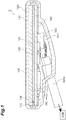
- FIG. 1 illustrates an intraoral sensor 1 according to a first embodiment.
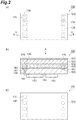
- FIGS. 2(a), 2(b), and 2(c) schematically illustrate intraoral sensors 100 and 101 as internal configurations of the intraoral sensor 1 illustrated in FIG. 1 .
- the intraoral sensor 1 according to the first embodiment includes a scintillator 110, a fiber optical plate (FOP) 120, an image sensor 130, a wiring board 140, an IC 150, a connector 160, and a sealed container 1020.
- FOP fiber optical plate
- the outline of the scintillator 110, the outline of the FOP 120, the outline of the image sensor 130, and the outline of the wiring board 140 may be slightly different from each other due to a manufacturing error.
- the difference equal to or less than a thickness of the FOP can be allowed. Therefore, the case where the outlines are different from each other in a range equal to or less than the thickness of the FOP is included in the range of "substantially aligned". The difference can be equal to or less than half of the thickness of the FOP.
- the outlines of the image sensor 130 and a supporting substrate 135 do not protrude from the outlines of the FOP 120 and the wiring board 140. This can be realized by designing dimensions of the image sensor 130 and the supporting substrate 135 to be smaller than dimensions of other layers in consideration of tolerance.
- the image sensor 130 is a so-called back-surface irradiation type image sensor, and a wiring layer is formed on the opposite side of a side where light enters (side of FOP 120).
- the thickness of the image sensor 130 is several ⁇ m to several tens ⁇ m.
- the image sensor 130 may be a CMOS type or a CCD type.
- the supporting substrate 135 which plays a role for supporting the image sensor 130 in a manufacturing process of the image sensor 130 is left.
- a material of the supporting substrate 135 is glass or Si.
- An electrode of the image sensor 130 and an electrode 141 of the wiring board 140 are electrically connected with bumps (ball-like conductor) 170 disposed in through-holes 136 provided in the supporting substrate 135.
- a gap between the supporting substrate 135 and the wiring board 140 formed by the bumps 170 is filled with an underfill 180 to the end so as to increase mechanical strength of bump connection and make it difficult to apply an external force to the end.
- a material of the bump 170 is a solder and the like, and a material of the underfill 180 is a one-pack epoxy resin and the like.
- the shape of the bump 170 is illustrated as a ball. However, it is not necessary for the shape of the bump 170 to be a ball, and any shape can be used.
- the single through-hole 136 houses the single bump 170. However, as illustrated in FIG. 2(c) , the single through-hole 136 may house the plurality bumps 170.
- the scintillator 110 is a member which emits fluorescence (scintillation light) by receiving radiation. This may be manufactured integrally with the FOP 120 as a fiber optical plate with scintillator (FOS).
- a method for connecting the scintillator 110 with the FOP 120 includes a method for directly depositing the scintillator 110 on the FOP 120, a method for placing a film-like scintillator 110 on the FOP 120, and a method for bonding the scintillator 110 to the FOP 120 with a transparent resin.
- the FOP 120 is a plate formed by bundling and bonding a large number of optical fibers formed of glass including metal atoms and the like, and has functions for transmitting light output from the scintillator 110 to the image sensor 130 and shielding radiation which has not been converted by the scintillator by the metal atoms (radiation transmitted through scintillator 110).
- the thickness of the FOP 120 is about 1.5 mm.
- the wiring board 140 is a substrate on which the electrode 141, wirings 142 and 143, and the like are disposed and is, for example, a glass epoxy substrate (plate-like substrate obtained by impregnating epoxy resin in glass fiber and executing thermosetting treatment) or a ceramic substrate.
- a through-hole 144 in which a conductive material such as solder is embedded is formed, and the electrode 141 and the wiring 142 are electrically connected to each other with the conductive material embedded in the through-hole 144.
- a thickness of the wiring board 140 is about 1 mm.
- the IC 150 is an integrated circuit, for example, which plays roles as follows.
- the connector 160 is a connector for connecting a cable (for example, USB cable 1010 illustrated in FIG. 1 ) which plays roles for deriving a signal from the IC 150 to the outside and supplying power or a signal from the outside to the IC 150 and the like.
- a cable for example, USB cable 1010 illustrated in FIG. 1
- the intraoral sensors 100 and 101 configured as described above are connected to the USB cable 1010 and sealed in the sealed container 1020 and used in a form of the intraoral sensor 1.
- the intraoral sensor 1 is inserted into an oral cavity of a patient and is disposed at a position which can be irradiated from a radiation source disposed outside the oral cavity and can detect radiation for transmitting teeth and gums.
- the intraoral sensors 100 and 101 in the intraoral sensor 1 detect the radiation which has transmitted the teeth and the gums and output signals of transparent images of the teeth and the gums.
- the intraoral sensor can be inserted into the oral cavity as it is and used.
- the outline of the scintillator 110, the outline of the FOP 120, the outline of the image sensor 130, and the outline of the wiring board 140 as viewed from the direction perpendicular to the first surface of the scintillator 110 (direction of arrow A) are substantially aligned. Therefore, an area occupied by a portion which does not contribute to imaging as viewed from the same direction can be made substantially zero. Therefore, it is possible to miniaturize the intraoral sensor as possible without sacrificing an effective area of the sensor.
- the stress concentrates on the step, and the concentration of the stress may be a cause of peeling between layers and breakage of each layer.
- the step is minimized in the intraoral sensors 1, 100, and 101, the peeling between the layers and the breakage of each layer hardly occur.
- the intraoral sensors 1, 100, and 101 since almost entire surfaces of the image sensor 130 and the wiring board 140 are covered with the FOP 120, such deterioration is prevented.
- the outline of the image sensor 130 is configured not to protrude from the outline of the FOP 120 and the outline of the wiring board 140. With this structure, even in a case where the outline of the image sensor 130, the outline of the FOP 120, and the outline of the wiring board 140 are slightly different from each other due to a manufacturing error and the like, the image sensor 130 which is most likely to be damaged is protected.
- the image sensor 130 be a back-surface irradiation type image sensor.
- the back-surface irradiation type image sensor it is not necessary to provide an electrode on a light receiving surface of the image sensor 130, and the entire surface of the image sensor can be easily covered with the FOP.
- an electrical output can be taken from an opposite side surface of the image sensor 130 from the FOP 120, the image sensor 130 and the wiring board 140 can be easily and electrically connected.
- sensitivity can be more improved in comparison with a case where a front-surface irradiation type image sensor is used.
- the supporting substrate 135 for supporting the image sensor is included between the image sensor 130 and the wiring board 140.
- the supporting substrate 135 since the image sensor 130 can be thinned as being supported by the supporting substrate 135 and can be connected to the wiring board 140, the back-surface irradiation type image sensor 130 which needs to be thinned can be easily manufactured and handled.
- the supporting substrate 135 is needed in a manufacturing process of the image sensor 130, there is no problem even if the supporting substrate 135 is left, and the mechanical strength can be maintained by leaving the supporting substrate 135. In a case where the fiber optical plate with scintillator (FOS) is used, the supporting substrate 135 may be left.
- FOS fiber optical plate with scintillator
- the image sensor 130 and the wiring board 140 are electrically connected to each other with the bumps 170. With this structure, the electrical connection between the image sensor 130 and the wiring board 140 can be easily and reliably performed.
- each of the intraoral sensors 1, 100, and 101 includes the layer of the underfill 180 between the supporting substrate 135 and the wiring board 140. With this structure, since the gap between the supporting substrate 135 and the wiring board 140 does not exist, the mechanical strength of each of the intraoral sensors 1, 100, and 101 is improved.
- the intraoral sensors 1, 100, and 101 include the connector 160 which is provided on the opposite surface of the wiring board 140 from the image sensor 130 and electrically connects the cable.
- the intraoral sensors 1, 100, and 101 can be more easily inserted into the oral cavity in comparison with a case where the connector 160 is provided at an edge of the wiring board 140 and the cable is led from the edge.
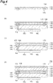
- FIG. 3 is a diagram of a process for manufacturing the image sensor 130 supported by the supporting substrate 135, and FIG. 4 is a diagram of the process for manufacturing the intraoral sensors 1, 100, and 101 subsequent to the process illustrated in FIG. 3 .
- a Si wafer 2130 in which elements configuring the plurality of image sensors 130 (impurity semiconductor region and electrode) are formed on a side of the first surface and a supporting substrate 2135 in which a through-hole 2136 is formed at a position corresponding to the position of each electrode of the plurality of image sensors 130 are prepared.
- the first surface of the Si wafer 2130 and the supporting substrate 2135 are positioned so that each electrode of each image sensor is exposed from the through-hole 2136 and are bonded to each other.
- a second surface side of the Si wafer 2130 is polished, and portions to be the plurality of image sensors 130 are thinned to have a predetermined thickness.
- the Si wafer 2130 is diced to be divided into the respective image sensors 130 supported by the supporting substrates 135.
- the wiring board 140 having the above structure is prepared in advance.
- the bump 170 is inserted into the through-hole 136 of the supporting substrate 135.
- an object which prevents the electrical conduction is removed by etching and the like before the bump 170 is inserted into the through-hole 136.
- the image sensor 130 supported by the supporting substrate 135 and the wiring board 140 are bonded with the bump 170, and in addition, the IC 150 and the connector 160 are mounted.
- the IC 150 and the connector 160 may be mounted before the bonding is performed or may be mounted after a process for filling the underfill 180 to be described next.
- a gap formed between the supporting substrate 135 and the wiring board 140 by the bump 170 is filled with the underfill 180.
- the FOP 120 and the scintillator 110 are bonded to the opposite side of the image sensor 130 from the supporting substrate 135 with a transparent resin.
- the FOP 120 and the scintillator 110 may be integrally manufactured as the fiber optical plate with scintillator (FOS) in advance as described above.
- a connector 1011 of the USB cable 1010 is connected to the connector 160 of the intraoral sensors 100 and 101 and is sealed in the sealed container 1020 through which the USB cable 1010 passes, and the form illustrated in FIG. 1 is realized.
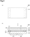
- FIGS. 5(a) and 5(b) illustrate an intraoral sensor 200 according to a second embodiment.
- the intraoral sensor 200 uses an embedded conductive member 270 instead of the bump 170 in the intraoral sensors 1, 100, and 101 according to the first embodiment.
- the intraoral sensor 200 is different from the intraoral sensors 1, 100, and 101 only in that point.
- the intraoral sensor 200 different from the intraoral sensors 1, 100, and 101, that is, a part regarding the embedded conductive member 270 will be mainly described.
- an electrode of an image sensor 230 and an electrode 241 of a wiring board 240 are embedded in a through-hole 236 provided in a supporting substrate 235, and the electrodes are electrically connected by the embedded conductive member 270 having a protruding portion 271. Furthermore, a gap between the supporting substrate 235 and the wiring board 240 formed by the protruding portion 271 of the embedded conductive member 270 is filled with an underfill 280 as in the intraoral sensors 1, 100, and 101.
- a material of the embedded conductive member 270 is a solder and the like.
- the intraoral sensor 200 according to the second embodiment configured as described above has the same effect as the intraoral sensors 1, 100, and 101 according to the first embodiment.
- FIG. 6 is a diagram of a process for manufacturing the intraoral sensor 200 from the image sensor 230 supported by the supporting substrate 235, in correspondence with FIG. 4 regarding the first embodiment.
- the wiring board 240 has the same configuration as the wiring board 140 in the first embodiment and is prepared in advance similar to the wiring board 140 in the first embodiment.
- the through-hole 236 of the supporting substrate 235 is filled with the embedded conductive member 270 so as to form the protruding portion 271.
- this can be realized by a method for repeating introduction and reflow (melting of solder ball) of a solder ball into the through-hole 236 by a predetermined number of times.
- an object which prevents the electrical conduction is removed by etching and the like before the embedded conductive member 270 is filled into the through-hole 236.
- the image sensor 230 supported by the supporting substrate 235 and the wiring board 240 are bonded to each other by the embedded conductive member 270 having the protruding portion 271, and in addition, an IC 250 and a connector 260 are mounted.
- the IC 250 and the connector 260 may be mounted before the bonding is performed or may be mounted after a process for filling the underfill 280 to be described next.
- a gap formed between the supporting substrate 235 and the wiring board 240 by the protruding portion 271 is filled with the underfill 280.
- FIG. 6(c) a gap formed between the supporting substrate 235 and the wiring board 240 by the protruding portion 271 is filled with the underfill 280.
- a FOP 220 and a scintillator 210 are bonded to the opposite side of the image sensor 230 from the supporting substrate 235.
- the FOP 220 and the scintillator 210 may be integrally manufactured as the fiber optical plate with scintillator (FOS) in advance as described above.
- FIGS. 7(a) and 7(b) illustrate an intraoral sensor 300 according to a third embodiment.
- the intraoral sensor 300 does not include the supporting substrate 135 of the intraoral sensors 1, 100, and 101 according to the first embodiment, and a scintillator 310 is a film-like scintillator.
- the intraoral sensor 300 is different from the intraoral sensors 1, 100, and 101 in only these two points.
- the supporting substrate 135 which plays a role for supporting the image sensor 130 in the manufacturing process of the image sensor 130 is left.
- the supporting substrate is removed in the intraoral sensor 300 according to the present embodiment.
- an electrode of an image sensor 330 and an electrode 341 of a wiring board 340 are electrically connected with bumps (ball-like conductor) 370 as in the first embodiment.
- a gap between the image sensor 330 and the wiring board 340 formed by the bumps 370 is filled with an underfill 380.
- a material of the bump 370 is a solder and the like, and a material of the underfill 380 is a one-pack epoxy resin and the like.
- the shape of the bump 370 is illustrated as a ball. However, it is not necessary for the shape of the bump 370 to be a ball, and any shape can be used.
- the scintillator 310 is a film-like scintillator and is configured to be attachable to a FOP 320.
- the intraoral sensor 300 according to the third embodiment configured as described above has the same effect as the intraoral sensors 1, 100, and 101 according to the first embodiment.
- the intraoral sensor 300 according to the third embodiment has an effect that the intraoral sensor is more thinned than the intraoral sensors 1, 100, and 101 according to the first embodiment and an effect that a process for forming a through-hole in a supporting substrate is unnecessary.
- a fiber optical plate with scintillator can be used as a scintillator.
- the scintillator 310 and the FOP 320 may be separated in the third embodiment.
- FIG. 8 is a diagram of a process for manufacturing the image sensor 330 supported by the FOP 320
- FIG. 9 is a diagram of the process for manufacturing the intraoral sensor 300 subsequent to the process illustrated in FIG. 8 .
- a Si wafer 2330 in which elements configuring the plurality of image sensors 330 (impurity semiconductor region and electrode) are formed on the side of the first surface and a supporting substrate 2335 are prepared.
- the through-hole 2136 has been formed in the supporting substrate 2135.
- the first surface of the Si wafer 2330 is bonded to the supporting substrate 2335.
- a second surface side of the Si wafer 2330 is polished, and portions to be the plurality of image sensors 330 are thinned to have a predetermined thickness.
- the Si wafer 2330 is diced to be divided into the respective image sensors 330 supported by the supporting substrates 335.
- the FOP 320 is bonded on the opposite side of the image sensor 330 supported by the individual supporting substrate 335 from the supporting substrate 335.
- FIG. 8(e) the FOP 320 is bonded on the opposite side of the image sensor 330 supported by the individual supporting substrate 335 from the supporting substrate 335.
- the supporting substrate 335 is removed. After the supporting substrate 335 has been removed, the thinned image sensor 330 is supported by the FOP 320.
- the wiring board 340 having the same structure as the wiring board 140 described above is prepared in advance.
- the image sensor 330 and the wiring board 340 are bonded with the bumps 370, and in addition, an IC 350 and a connector 360 are mounted.
- the IC 350 and the connector 360 may be mounted before the bonding is performed or may be mounted after a process for filling the underfill 380 to be described next.
- a gap formed between the image sensor 330 and the wiring board 340 by the bumps 370 is filled with the underfill 380.
- the sheet-like scintillator 310 is bonded to the opposite side of the FOP 320 from the image sensor 330.
- the one aspect of the present invention is not limited to the embodiments.
- the shapes of the intraoral sensors 100, 200, and 300 illustrated in the top view are rectangles. However, other shapes such as a polygon, a circle, and an ellipse may be used.
- a cross-sectional shape of each of the through-holes 136 and 236 of the supporting substrate is a square or a rectangle.
- other shapes such as a polygon, a circle, and an ellipse may be used.
- the ICs 150, 250, and 350 are respectively provided in the intraoral sensors 100, 200, and 300 one each.
- the plurality of ICs may be provided in each of the intraoral sensors 100, 101, 200, and 300.
- the cable is the USB cable 1010, and the connectors 160, 260, and 360 are connecters connected to the USB cable 1010.
- the cable may be a cable other than the USB cable, and the connectors 160, 260, and 360 may be a connector compatible with cables other than the USB cable.
- the image sensors 130, 230, and 330 are back-surface incidence type image sensors.
- a front-surface incidence type image sensor may be used.
Landscapes
- Health & Medical Sciences (AREA)
- Life Sciences & Earth Sciences (AREA)
- High Energy & Nuclear Physics (AREA)
- Molecular Biology (AREA)
- Physics & Mathematics (AREA)
- Engineering & Computer Science (AREA)
- Medical Informatics (AREA)
- General Physics & Mathematics (AREA)
- Spectroscopy & Molecular Physics (AREA)
- Nuclear Medicine, Radiotherapy & Molecular Imaging (AREA)
- Surgery (AREA)
- Oral & Maxillofacial Surgery (AREA)
- Dentistry (AREA)
- Optics & Photonics (AREA)
- Pathology (AREA)
- Radiology & Medical Imaging (AREA)
- Biomedical Technology (AREA)
- Heart & Thoracic Surgery (AREA)
- Biophysics (AREA)
- Animal Behavior & Ethology (AREA)
- General Health & Medical Sciences (AREA)
- Public Health (AREA)
- Veterinary Medicine (AREA)
- Apparatus For Radiation Diagnosis (AREA)
- Solid State Image Pick-Up Elements (AREA)
- Measurement Of Radiation (AREA)
Abstract
Description
- One aspect of the present invention relates to an intraoral sensor.
- Conventionally, a dental intraoral sensor has been known. For example, in
Patent Literature 1, a radiation imaging apparatus used as being mounted on a back of a tooth in an oral cavity is described as a fourth embodiment. The radiation imaging apparatus includes a scintillator, a fiber optical plate (FOP), a CMOS imaging element, a base, and the like. - A dental intraoral sensor is also disclosed in
Patent Literature 2. -
- Patent Literature 1: Japanese Unexamined Patent Publication No.
2003-66148 - Patent Literature 2: Japanese Unexamined Patent Publication No.
H5-130990 - An intraoral sensor disclosed in
Patent Literatures - One aspect of the present invention is made to solve the problems, and an object of the present invention is to provide an intraoral sensor which is miniaturized as possible without sacrificing an effective area of a sensor and has a structure which is hardly damaged.
- An intraoral sensor according to one aspect of the present invention includes a scintillator including a first surface and a second surface, a fiber optical plate disposed on the second surface side of the scintillator, an image sensor disposed on an opposite side of the fiber optical plate from the scintillator, and a wiring board disposed on an opposite side of the image sensor from the fiber optical plate, in which, when viewed from a direction perpendicular to the first surface of the scintillator, an outline of the scintillator, an outline of the fiber optical plate, an outline of the image sensor, and an outline of the wiring board are substantially aligned.
- In the intraoral sensor, since the outline of the scintillator, the outline of the fiber optical plate, the outline of the image sensor, and the outline of the wiring board as viewed from the direction perpendicular to the first surface of the scintillator are substantially aligned, an area occupied by a portion which does not contribute to imaging as viewed from the same direction can be made substantially zero. Therefore, it is possible to miniaturize the intraoral sensor as possible without sacrificing the effective area of the sensor. Furthermore, if there is a step between edges of layers of the scintillator, the fiber optical plate, the image sensor, and the wiring board, a stress concentrates on the step, and the concentration of the stress may be a cause of peeling between layers and breakage of each layer. However, since the step is minimized in one aspect of the present invention, the peeling between the layers and the breakage of each layer hardly occur. In addition, where there is a portion in the image sensor and the wiring board which is not covered with the fiber optical plate, radiation having high energy is applied to the portion, and deterioration is facilitated. However, in one aspect of the present invention, since almost entire surfaces of the image sensor and the wiring board are covered with the fiber optical plate, such deterioration can be prevented.
- In the intraoral sensor according to one aspect of the present invention, the outline of the image sensor may be configured not to protrude from the outline of the fiber optical plate and the outline of the wiring board. In this case, in a case where the outline of the image sensor, the outline of the fiber optical plate, and the outline of the wiring board are different from each other due to a manufacturing error and the like, the image sensor which is most likely to be damaged can be protected.
- In the intraoral sensor according to one aspect of the present invention, the image sensor may be a back-surface irradiation type image sensor. In this case, since an electrical output can be taken from an opposite surface of the image sensor from the fiber optical plate, the image sensor and the wiring board can be easily and electrically connected.
- The intraoral sensor according to one aspect of the present invention may include a supporting substrate for supporting the image sensor, between the image sensor and the wiring board. When the supporting substrate is used, the image sensor can be thinned in a state of being supported by the supporting substrate and can be connected to the wiring board. Therefore, the back-surface irradiation type image sensor which needs to be thinned can be easily manufactured and handled.
- In the intraoral sensor according to one aspect of the present invention, the scintillator may be a film-like scintillator. In this case, the scintillator can be easily attached by an arbitrary process.
- In the intraoral sensor according to one aspect of the present invention, the image sensor and the wiring board may be connected to each other with a ball-like conductor. In this case, the electrical connection between the image sensor and the wiring board can be easily and reliably performed.
- The intraoral sensor according to one aspect of the present invention may include an underfill layer between the image sensor and the wiring board. In this case, since a gap between the image sensor and the wiring board does not exist, mechanical strength of the intraoral sensor is improved.
- The intraoral sensor according to one aspect of the present invention may include a connector which is provided on an opposite surface of the wiring board from the image sensor and electrically connects a cable. In this case, the cable can be led from the opposite surface of the wiring board from the image sensor. Therefore, the intraoral sensor can be more easily inserted into the oral cavity in comparison with a structure in which the connector is provided at an edge of the wiring board and the cable is led from the edge.
- The intraoral sensor according to one aspect of the present invention may include a sealed container. The scintillator, the fiber optical plate, the image sensor, and the wiring board may be sealed in the sealed container. In this case, the intraoral sensor can be inserted into the oral cavity and used.
- According to one aspect of the present invention, it is possible to provide an intraoral sensor which is miniaturized as possible without sacrificing an effective area of a sensor and has a structure which is hardly damaged.
-
-
FIG. 1 is a diagram of an intraoral sensor according to a first embodiment. -
FIG. 2 is a schematic diagram of an intraoral sensor as an internal configuration of the intraoral sensor illustrated inFIG. 1 .FIG. 2(a) is a top view,FIG. 2(b) is a cross-sectional diagram taken along a b-b line inFIG. 2(a), and FIG. 2(c) is a diagram of a modification ofFig. 2(a) . -
FIG. 3 is a diagram of a process for manufacturing an image sensor supported by a supporting substrate of the intraoral sensor according to the first embodiment. -
FIG. 4 is a diagram of the process for manufacturing the intraoral sensor according to the first embodiment subsequent to the process illustrated inFIG. 3 . -
FIG. 5 is a diagram of an intraoral sensor according to a second embodiment. -
FIG. 6 is a diagram of a part of a process for manufacturing the intraoral sensor according to the second embodiment. -
FIG. 7 is a diagram of an intraoral sensor according to a third embodiment. -
FIG. 8 is a diagram of a process for manufacturing an image sensor supported by a supporting substrate of the intraoral sensor according to the third embodiment. -
FIG. 9 is a diagram of a process for manufacturing the intraoral sensor according to the third embodiment subsequent to the process illustrated inFIG. 8 . - Hereinafter, embodiments according to one aspect of the present invention will be described with reference to the drawings. In the drawings, the same or corresponding parts are denoted with the same reference numeral. Furthermore, there is a case where dimensions and dimensional ratios of each unit in the drawings do not indicate actual dimensions and dimensional ratios.
-
FIG. 1 illustrates anintraoral sensor 1 according to a first embodiment.FIGS. 2(a), 2(b), and 2(c) schematically illustrateintraoral sensors intraoral sensor 1 illustrated inFIG. 1 . As illustrated inFIGS. 1 and2(a) to 2(c) , theintraoral sensor 1 according to the first embodiment includes ascintillator 110, a fiber optical plate (FOP) 120, animage sensor 130, awiring board 140, anIC 150, aconnector 160, and a sealedcontainer 1020. When viewed from a direction of an arrow A inFIG. 2(b) (direction perpendicular to first surface of scintillator), an outline of thescintillator 110, an outline of theFOP 120, an outline of theimage sensor 130, and an outline of thewiring board 140 are substantially aligned. - Here, the outline of the
scintillator 110, the outline of theFOP 120, the outline of theimage sensor 130, and the outline of thewiring board 140 may be slightly different from each other due to a manufacturing error. However, the difference equal to or less than a thickness of the FOP can be allowed. Therefore, the case where the outlines are different from each other in a range equal to or less than the thickness of the FOP is included in the range of "substantially aligned". The difference can be equal to or less than half of the thickness of the FOP. - Furthermore, even when the difference is generated, the outlines of the
image sensor 130 and a supportingsubstrate 135 do not protrude from the outlines of theFOP 120 and thewiring board 140. This can be realized by designing dimensions of theimage sensor 130 and the supportingsubstrate 135 to be smaller than dimensions of other layers in consideration of tolerance. - The
image sensor 130 is a so-called back-surface irradiation type image sensor, and a wiring layer is formed on the opposite side of a side where light enters (side of FOP 120). In an example, the thickness of theimage sensor 130 is several µm to several tens µm. Theimage sensor 130 may be a CMOS type or a CCD type. - Furthermore, on the side of the
image sensor 130 where the wiring layer is formed, the supportingsubstrate 135 which plays a role for supporting theimage sensor 130 in a manufacturing process of theimage sensor 130 is left. In an example, a material of the supportingsubstrate 135 is glass or Si. - An electrode of the
image sensor 130 and anelectrode 141 of thewiring board 140 are electrically connected with bumps (ball-like conductor) 170 disposed in through-holes 136 provided in the supportingsubstrate 135. A gap between the supportingsubstrate 135 and thewiring board 140 formed by thebumps 170 is filled with anunderfill 180 to the end so as to increase mechanical strength of bump connection and make it difficult to apply an external force to the end. A material of thebump 170 is a solder and the like, and a material of theunderfill 180 is a one-pack epoxy resin and the like. - In
FIG. 2 , the shape of thebump 170 is illustrated as a ball. However, it is not necessary for the shape of thebump 170 to be a ball, and any shape can be used. InFIG. 2(a) , it is illustrated that the single through-hole 136 houses thesingle bump 170. However, as illustrated inFIG. 2(c) , the single through-hole 136 may house the plurality bumps 170. - The
scintillator 110 is a member which emits fluorescence (scintillation light) by receiving radiation. This may be manufactured integrally with theFOP 120 as a fiber optical plate with scintillator (FOS). A method for connecting thescintillator 110 with theFOP 120 includes a method for directly depositing thescintillator 110 on theFOP 120, a method for placing a film-like scintillator 110 on theFOP 120, and a method for bonding thescintillator 110 to theFOP 120 with a transparent resin. - The
FOP 120 is a plate formed by bundling and bonding a large number of optical fibers formed of glass including metal atoms and the like, and has functions for transmitting light output from thescintillator 110 to theimage sensor 130 and shielding radiation which has not been converted by the scintillator by the metal atoms (radiation transmitted through scintillator 110). In an example, the thickness of theFOP 120 is about 1.5 mm. - The
wiring board 140 is a substrate on which theelectrode 141,wirings wiring board 140, a through-hole 144 in which a conductive material such as solder is embedded is formed, and theelectrode 141 and thewiring 142 are electrically connected to each other with the conductive material embedded in the through-hole 144. In an example, a thickness of thewiring board 140 is about 1 mm. - The
IC 150 is an integrated circuit, for example, which plays roles as follows. - a. to supply a control clock signal to the
image sensor 130. - b. to convert a supply voltage (for example, 5 V) from a cable into a voltage at which the
image sensor 130 and other ICs (not shown) can operate. - c. to convert an image signal from the
image sensor 130 into a format (for example, waveform conforming to USB standard) which can be transferred to an external device such as a personal computer. - d. to convert an instruction signal from a personal computer and the like into a format which can be transferred to the
image sensor 130. - e. to hold information of the
image sensor 130 and the like in a memory. - The
connector 160 is a connector for connecting a cable (for example,USB cable 1010 illustrated inFIG. 1 ) which plays roles for deriving a signal from theIC 150 to the outside and supplying power or a signal from the outside to theIC 150 and the like. - As illustrated in
FIG. 1 , theintraoral sensors USB cable 1010 and sealed in the sealedcontainer 1020 and used in a form of theintraoral sensor 1. - The
intraoral sensor 1 is inserted into an oral cavity of a patient and is disposed at a position which can be irradiated from a radiation source disposed outside the oral cavity and can detect radiation for transmitting teeth and gums. When the radiation is emitted from the radiation source, theintraoral sensors intraoral sensor 1 detect the radiation which has transmitted the teeth and the gums and output signals of transparent images of the teeth and the gums. - According to the
intraoral sensor 1, the intraoral sensor can be inserted into the oral cavity as it is and used. - Furthermore, in the
intraoral sensors scintillator 110, the outline of theFOP 120, the outline of theimage sensor 130, and the outline of thewiring board 140 as viewed from the direction perpendicular to the first surface of the scintillator 110 (direction of arrow A) are substantially aligned. Therefore, an area occupied by a portion which does not contribute to imaging as viewed from the same direction can be made substantially zero. Therefore, it is possible to miniaturize the intraoral sensor as possible without sacrificing an effective area of the sensor. Furthermore, if there is a step between edges of each layers of thescintillator 110, theFOP 120, theimage sensor 130, and thewiring board 140, the stress concentrates on the step, and the concentration of the stress may be a cause of peeling between layers and breakage of each layer. However, since the step is minimized in theintraoral sensors image sensor 130 and thewiring board 140 which is not covered with theFOP 120, radiation having high energy is applied to the portion, and deterioration is facilitated. However, in theintraoral sensors image sensor 130 and thewiring board 140 are covered with theFOP 120, such deterioration is prevented. - Furthermore, in the
intraoral sensors image sensor 130 is configured not to protrude from the outline of theFOP 120 and the outline of thewiring board 140. With this structure, even in a case where the outline of theimage sensor 130, the outline of theFOP 120, and the outline of thewiring board 140 are slightly different from each other due to a manufacturing error and the like, theimage sensor 130 which is most likely to be damaged is protected. - In the
intraoral sensors image sensor 130 be a back-surface irradiation type image sensor. By using the back-surface irradiation type image sensor, it is not necessary to provide an electrode on a light receiving surface of theimage sensor 130, and the entire surface of the image sensor can be easily covered with the FOP. Furthermore, since an electrical output can be taken from an opposite side surface of theimage sensor 130 from theFOP 120, theimage sensor 130 and thewiring board 140 can be easily and electrically connected. In addition, sensitivity can be more improved in comparison with a case where a front-surface irradiation type image sensor is used. - Furthermore, in the
intraoral sensors substrate 135 for supporting the image sensor is included between theimage sensor 130 and thewiring board 140. When the supportingsubstrate 135 is used, since theimage sensor 130 can be thinned as being supported by the supportingsubstrate 135 and can be connected to thewiring board 140, the back-surface irradiationtype image sensor 130 which needs to be thinned can be easily manufactured and handled. Although the supportingsubstrate 135 is needed in a manufacturing process of theimage sensor 130, there is no problem even if the supportingsubstrate 135 is left, and the mechanical strength can be maintained by leaving the supportingsubstrate 135. In a case where the fiber optical plate with scintillator (FOS) is used, the supportingsubstrate 135 may be left. This is because, although a scintillator portion of the FOS has a heat-sensitive property, a bonding process to thewiring board 140 in which theimage sensor 130 is exposed to a high temperature can be completed in a state where the supportingsubstrate 135 is sandwiched between theimage sensor 130 and thewiring board 140 before a process for bonding the FOS to theimage sensor 130. - Furthermore, in the
intraoral sensors image sensor 130 and thewiring board 140 are electrically connected to each other with thebumps 170. With this structure, the electrical connection between theimage sensor 130 and thewiring board 140 can be easily and reliably performed. - Furthermore, each of the
intraoral sensors underfill 180 between the supportingsubstrate 135 and thewiring board 140. With this structure, since the gap between the supportingsubstrate 135 and thewiring board 140 does not exist, the mechanical strength of each of theintraoral sensors - Furthermore, the
intraoral sensors connector 160 which is provided on the opposite surface of thewiring board 140 from theimage sensor 130 and electrically connects the cable. With this structure, since the cable can be led from the opposite surface of thewiring board 140 from theimage sensor 130, theintraoral sensors connector 160 is provided at an edge of thewiring board 140 and the cable is led from the edge. - Next, an example of a manufacturing method of the
intraoral sensors FIGS. 3 and4 . -
FIG. 3 is a diagram of a process for manufacturing theimage sensor 130 supported by the supportingsubstrate 135, andFIG. 4 is a diagram of the process for manufacturing theintraoral sensors FIG. 3 . - First, as illustrated in
FIG. 3(a) , a Si wafer 2130 in which elements configuring the plurality of image sensors 130 (impurity semiconductor region and electrode) are formed on a side of the first surface and a supporting substrate 2135 in which a through-hole 2136 is formed at a position corresponding to the position of each electrode of the plurality ofimage sensors 130 are prepared. Next, as illustrated inFIG. 3(b) , the first surface of the Si wafer 2130 and the supporting substrate 2135 are positioned so that each electrode of each image sensor is exposed from the through-hole 2136 and are bonded to each other. Next, as illustrated inFIG. 3(c) , a second surface side of the Si wafer 2130 is polished, and portions to be the plurality ofimage sensors 130 are thinned to have a predetermined thickness. Next, as illustrated inFIG. 3(d) , the Si wafer 2130 is diced to be divided into therespective image sensors 130 supported by the supportingsubstrates 135. On the other hand, thewiring board 140 having the above structure is prepared in advance. - Next, as illustrated in
FIG. 4(a) , thebump 170 is inserted into the through-hole 136 of the supportingsubstrate 135. In a case where there is a possibility that electrical conduction with thebump 170 is prevented due to adhesion of adhesive to the surface of the electrode of theimage sensor 130 exposed in the through-hole 136 and the like, an object which prevents the electrical conduction is removed by etching and the like before thebump 170 is inserted into the through-hole 136. Next, as illustrated inFIG. 4(b) , theimage sensor 130 supported by the supportingsubstrate 135 and thewiring board 140 are bonded with thebump 170, and in addition, theIC 150 and theconnector 160 are mounted. TheIC 150 and theconnector 160 may be mounted before the bonding is performed or may be mounted after a process for filling theunderfill 180 to be described next. Next, as illustrated inFIG. 4(c) , a gap formed between the supportingsubstrate 135 and thewiring board 140 by thebump 170 is filled with theunderfill 180. Next, as illustrated inFIG. 4(d) , theFOP 120 and thescintillator 110 are bonded to the opposite side of theimage sensor 130 from the supportingsubstrate 135 with a transparent resin. TheFOP 120 and thescintillator 110 may be integrally manufactured as the fiber optical plate with scintillator (FOS) in advance as described above. - Finally, a
connector 1011 of theUSB cable 1010 is connected to theconnector 160 of theintraoral sensors container 1020 through which theUSB cable 1010 passes, and the form illustrated inFIG. 1 is realized. -
FIGS. 5(a) and 5(b) illustrate anintraoral sensor 200 according to a second embodiment. - As illustrated in
FIGS. 5(a) and 5(b) , theintraoral sensor 200 uses an embeddedconductive member 270 instead of thebump 170 in theintraoral sensors intraoral sensor 200 is different from theintraoral sensors - Hereinafter, a part of the
intraoral sensor 200 different from theintraoral sensors conductive member 270 will be mainly described. - As illustrated in
FIGS. 5(a) and 5(b) , in theintraoral sensor 200, an electrode of animage sensor 230 and anelectrode 241 of awiring board 240 are embedded in a through-hole 236 provided in a supportingsubstrate 235, and the electrodes are electrically connected by the embeddedconductive member 270 having a protrudingportion 271. Furthermore, a gap between the supportingsubstrate 235 and thewiring board 240 formed by the protrudingportion 271 of the embeddedconductive member 270 is filled with anunderfill 280 as in theintraoral sensors conductive member 270 is a solder and the like. - The
intraoral sensor 200 according to the second embodiment configured as described above has the same effect as theintraoral sensors - In the first embodiment, regarding the through-
hole 136, a modification illustrated inFIG. 2(c) may be employed. However, such a modification cannot be employed in the second embodiment. This is because insulation between the electrodes cannot be secured unless the through-hole is separated for each electrode in the second embodiment. - Next, an example of a manufacturing method of the
intraoral sensor 200 described above will be described with reference toFIG. 6 . - Note that a process for manufacturing the
image sensor 230 supported by the supportingsubstrate 235 is the same as the process for manufacturing theimage sensor 130 supported by the supportingsubstrate 135 illustrated inFIG. 3 . Therefore, illustration and description of the process will be omitted. -
FIG. 6 is a diagram of a process for manufacturing theintraoral sensor 200 from theimage sensor 230 supported by the supportingsubstrate 235, in correspondence withFIG. 4 regarding the first embodiment. - Here, the
wiring board 240 has the same configuration as thewiring board 140 in the first embodiment and is prepared in advance similar to thewiring board 140 in the first embodiment. - First, as illustrated in
FIG. 6(a) , the through-hole 236 of the supportingsubstrate 235 is filled with the embeddedconductive member 270 so as to form the protrudingportion 271. For example, this can be realized by a method for repeating introduction and reflow (melting of solder ball) of a solder ball into the through-hole 236 by a predetermined number of times. In a case where there is a possibility that electrical conduction with the embeddedconductive member 270 is prevented due to adhesion of adhesive to the surface of the electrode of theimage sensor 230 exposed in the through-hole 236 and the like, an object which prevents the electrical conduction is removed by etching and the like before the embeddedconductive member 270 is filled into the through-hole 236. Next, as illustrated inFIG 6(b) , theimage sensor 230 supported by the supportingsubstrate 235 and thewiring board 240 are bonded to each other by the embeddedconductive member 270 having the protrudingportion 271, and in addition, anIC 250 and aconnector 260 are mounted. TheIC 250 and theconnector 260 may be mounted before the bonding is performed or may be mounted after a process for filling theunderfill 280 to be described next. Next, as illustrated inFIG. 6(c) , a gap formed between the supportingsubstrate 235 and thewiring board 240 by the protrudingportion 271 is filled with theunderfill 280. Next, as illustrated inFIG. 6 (d) , aFOP 220 and ascintillator 210 are bonded to the opposite side of theimage sensor 230 from the supportingsubstrate 235. TheFOP 220 and thescintillator 210 may be integrally manufactured as the fiber optical plate with scintillator (FOS) in advance as described above. -
FIGS. 7(a) and 7(b) illustrate anintraoral sensor 300 according to a third embodiment. - As illustrated in
FIGS. 7(a) and 7(b) , theintraoral sensor 300 does not include the supportingsubstrate 135 of theintraoral sensors scintillator 310 is a film-like scintillator. Theintraoral sensor 300 is different from theintraoral sensors - Hereinafter, a part of the
intraoral sensor 300 different from theintraoral sensors - In the
intraoral sensors image sensor 130 where the wiring layer is formed, the supportingsubstrate 135 which plays a role for supporting theimage sensor 130 in the manufacturing process of theimage sensor 130 is left. However, the supporting substrate is removed in theintraoral sensor 300 according to the present embodiment. - Then, an electrode of an
image sensor 330 and anelectrode 341 of awiring board 340 are electrically connected with bumps (ball-like conductor) 370 as in the first embodiment. A gap between theimage sensor 330 and thewiring board 340 formed by thebumps 370 is filled with anunderfill 380. A material of thebump 370 is a solder and the like, and a material of theunderfill 380 is a one-pack epoxy resin and the like. - In
FIG. 7 , the shape of thebump 370 is illustrated as a ball. However, it is not necessary for the shape of thebump 370 to be a ball, and any shape can be used. - The
scintillator 310 is a film-like scintillator and is configured to be attachable to aFOP 320. - The
intraoral sensor 300 according to the third embodiment configured as described above has the same effect as theintraoral sensors intraoral sensor 300 according to the third embodiment has an effect that the intraoral sensor is more thinned than theintraoral sensors - Note that, in the first embodiment, a fiber optical plate with scintillator (FOS) can be used as a scintillator. However, the
scintillator 310 and theFOP 320 may be separated in the third embodiment. - Next, an example of a manufacturing method of the
intraoral sensor 300 described above will be described with reference toFIGS. 8 and9 . -
FIG. 8 is a diagram of a process for manufacturing theimage sensor 330 supported by theFOP 320, andFIG. 9 is a diagram of the process for manufacturing theintraoral sensor 300 subsequent to the process illustrated inFIG. 8 . - First, as illustrated in
FIG. 8(a) , aSi wafer 2330 in which elements configuring the plurality of image sensors 330 (impurity semiconductor region and electrode) are formed on the side of the first surface and a supportingsubstrate 2335 are prepared. InFIG. 3 according to the first embodiment, the through-hole 2136 has been formed in the supporting substrate 2135. However, it is not necessary to provide a through-hole in the supportingsubstrate 2335 according to the present embodiment. - Next, as illustrated in
FIG. 8(b) , the first surface of theSi wafer 2330 is bonded to the supportingsubstrate 2335. Next, as illustrated inFIG. 8(c) , a second surface side of theSi wafer 2330 is polished, and portions to be the plurality ofimage sensors 330 are thinned to have a predetermined thickness. Next, as illustrated inFIG. 8(d) , theSi wafer 2330 is diced to be divided into therespective image sensors 330 supported by the supportingsubstrates 335. Next, as illustrated inFIG. 8(e) , theFOP 320 is bonded on the opposite side of theimage sensor 330 supported by theindividual supporting substrate 335 from the supportingsubstrate 335. Next, as illustrated inFIG. 8(f) , the supportingsubstrate 335 is removed. After the supportingsubstrate 335 has been removed, the thinnedimage sensor 330 is supported by theFOP 320. On the other hand, thewiring board 340 having the same structure as thewiring board 140 described above is prepared in advance. - Next, as illustrated in
FIG. 9(a) , theimage sensor 330 and thewiring board 340 are bonded with thebumps 370, and in addition, anIC 350 and aconnector 360 are mounted. TheIC 350 and theconnector 360 may be mounted before the bonding is performed or may be mounted after a process for filling theunderfill 380 to be described next. Next, as illustrated inFIG. 9(b) , a gap formed between theimage sensor 330 and thewiring board 340 by thebumps 370 is filled with theunderfill 380. Next, as illustrated inFIG. 9(c) , the sheet-like scintillator 310 is bonded to the opposite side of theFOP 320 from theimage sensor 330. - According to the manufacturing method illustrated in
FIGS. 8 and9 , bonding with high temperature is performed after theimage sensor 330 has been bonded to theFOP 320. Therefore, theFOP 320 needs to be able to withstand high temperature. However, since thescintillator 310 is bonded to theFOP 320 after the bonding, thescintillator 310 is not damaged by high temperature. - Although the embodiments according to one aspect of the present invention have been described above, the one aspect of the present invention is not limited to the embodiments. For example, in the embodiments, the shapes of the
intraoral sensors - In the embodiments, a cross-sectional shape of each of the through-
holes - In the
intraoral sensors ICs intraoral sensors intraoral sensors - In the embodiments, the cable is the
USB cable 1010, and theconnectors USB cable 1010. However, the cable may be a cable other than the USB cable, and theconnectors - In the embodiments, the
image sensors - It is possible to provide an intraoral sensor which is miniaturized as possible without sacrificing an effective area of a sensor and has a structure which is hardly damaged.
-
- 1, 100, 101, 200, 300 intraoral sensor
- 110, 210, 310 scintillator
- 120,220,320 FOP
- 130, 230, 330 image sensor
- 135, 235, 335,2135, 2335 supporting substrate
- 136, 236, 2136 through-hole of supporting substrate
- 140, 240, 340 wiring board
- 141,241,341 electrode of wiring board
- 142, 143 wiring of wiring board
- 150,250,350 IC
- 160, 260, 360 connector (intraoral sensor side)
- 170, 370 bump
- 270 embedded conductive member
- 180, 280, 380 underfill
- 2130, 2330 Si wafer
- 1010 USB cable
- 1011 connector (USB cable side)
- 1020 sealed container
Claims (9)
- An intraoral sensor comprising:a scintillator including a first surface and a second surface;a fiber optical plate disposed on the second surface side of the scintillator;an image sensor disposed on an opposite side of the fiber optical plate from the scintillator; anda wiring board disposed on an opposite side of the image sensor from the fiber optical plate,wherein, when viewed from a direction perpendicular to the first surface of the scintillator, an outline of the scintillator, an outline of the fiber optical plate, an outline of the image sensor, and an outline of the wiring board are substantially aligned.
- The intraoral sensor according to claim 1, wherein the outline of the image sensor does not protrude from the outline of the fiber optical plate and the outline of the wiring board.
- The intraoral sensor according to claim 1 or 2, wherein the image sensor is a back-surface irradiation type image sensor.
- The intraoral sensor according to claim 3, comprising: a supporting substrate configured to support the image sensor between the image sensor and the wiring board.
- The intraoral sensor according to any one of claims 1 to 4, wherein the scintillator is a film-like scintillator.
- The intraoral sensor according to any one of claims 1 to 5, wherein the image sensor and the wiring board are connected to each other with a ball-like conductor.
- The intraoral sensor according to any one of claims 1 to 6, comprising: an underfill layer between the image sensor and the wiring board.
- The intraoral sensor according to any one of claims 1 to 7, comprising: a connector configured to electrically connect a cable and be provided on an opposite surface of the wiring board from the image sensor.
- The intraoral sensor according to any one of claims 1 to 8, further comprising: a sealed container, wherein the scintillator, the fiber optical plate, the image sensor, and the wiring board are sealed in the sealed container.
Applications Claiming Priority (2)
| Application Number | Priority Date | Filing Date | Title |
|---|---|---|---|
| JP2016243263 | 2016-12-15 | ||
| PCT/JP2017/040949 WO2018110184A1 (en) | 2016-12-15 | 2017-11-14 | Intraoral sensor |
Publications (3)
| Publication Number | Publication Date |
|---|---|
| EP3556295A1 true EP3556295A1 (en) | 2019-10-23 |
| EP3556295A4 EP3556295A4 (en) | 2020-08-05 |
| EP3556295B1 EP3556295B1 (en) | 2022-07-27 |
Family
ID=62558601
Family Applications (1)
| Application Number | Title | Priority Date | Filing Date |
|---|---|---|---|
| EP17880438.1A Active EP3556295B1 (en) | 2016-12-15 | 2017-11-14 | Intraoral sensor |
Country Status (4)
| Country | Link |
|---|---|
| US (1) | US20190331807A1 (en) |
| EP (1) | EP3556295B1 (en) |
| JP (1) | JPWO2018110184A1 (en) |
| WO (1) | WO2018110184A1 (en) |
Families Citing this family (1)
| Publication number | Priority date | Publication date | Assignee | Title |
|---|---|---|---|---|
| JP2026048259A (en) * | 2024-09-05 | 2026-03-17 | キヤノン株式会社 | Radiation imaging device and radiation imaging system |
Family Cites Families (8)
| Publication number | Priority date | Publication date | Assignee | Title |
|---|---|---|---|---|
| JPH05130990A (en) | 1991-10-25 | 1993-05-28 | Hamamatsu Photonics Kk | Medical X-ray image detector with automatic exposure function |
| JP3836208B2 (en) * | 1997-04-09 | 2006-10-25 | 浜松ホトニクス株式会社 | Small medical X-ray image detection device |
| JP2003066148A (en) | 2000-07-10 | 2003-03-05 | Canon Inc | Imaging device, radiation imaging device, and image processing system |
| US6800836B2 (en) * | 2000-07-10 | 2004-10-05 | Canon Kabushiki Kaisha | Image pickup device, radiation image pickup device and image processing system |
| WO2012174509A1 (en) * | 2011-06-16 | 2012-12-20 | Suni Medical Imaging, Inc. | X-ray image sensor |
| US20130129044A1 (en) * | 2011-11-18 | 2013-05-23 | Cyber Medical Imaging, Inc. | Intraoral Radiographic Imaging Sensors with Minimized Mesial Imaging Dead Space |
| WO2016022007A1 (en) * | 2014-08-08 | 2016-02-11 | 주식회사 레이언스 | Intraoral sensor |
| EP3244800A1 (en) * | 2015-01-12 | 2017-11-22 | Real Time Imaging Technologies, LLC | Low-dose x-ray imaging system |
-
2017
- 2017-11-14 EP EP17880438.1A patent/EP3556295B1/en active Active
- 2017-11-14 WO PCT/JP2017/040949 patent/WO2018110184A1/en not_active Ceased
- 2017-11-14 JP JP2018556515A patent/JPWO2018110184A1/en active Pending
- 2017-11-14 US US16/467,518 patent/US20190331807A1/en not_active Abandoned
Also Published As
| Publication number | Publication date |
|---|---|
| JPWO2018110184A1 (en) | 2019-10-31 |
| US20190331807A1 (en) | 2019-10-31 |
| EP3556295B1 (en) | 2022-07-27 |
| WO2018110184A1 (en) | 2018-06-21 |
| EP3556295A4 (en) | 2020-08-05 |
Similar Documents
| Publication | Publication Date | Title |
|---|---|---|
| US6479827B1 (en) | Image sensing apparatus | |
| JP4000507B2 (en) | Method for manufacturing solid-state imaging device | |
| CN104135933A (en) | Compact sensor module | |
| US10115878B2 (en) | Optical sensor | |
| KR100978307B1 (en) | Optical Passive Optical Alignment Method, Optical Device Packaging System and Optical Module Using the Same | |
| EP4145508A1 (en) | Optical sensor encapsulation structure and electronic device | |
| US11049899B2 (en) | Encapsulation structure of image sensing chip, and encapsulation method therefor | |
| CN106455952B (en) | Camera unit, wiring board with cable, and manufacturing method of wiring board with cable | |
| JP6097644B2 (en) | Imaging module, ranging module, imaging module with insulating tube, imaging module with lens, and endoscope | |
| US20190280036A1 (en) | Detector module, detector, imaging apparatus and method of manufacturing a detector module | |
| EP3556295B1 (en) | Intraoral sensor | |
| KR101868760B1 (en) | Hall sensor manufacturing method, hall sensor, and lens module | |
| JP2014204275A (en) | Imaging apparatus, manufacturing method of imaging apparatus, and imaging module | |
| KR20200046030A (en) | Intraoral sensor and method for manufacturing intraoral sensor | |
| US20140367578A1 (en) | X-ray image sensor | |
| JP6535087B2 (en) | Imaging module and manufacturing method of imaging module | |
| WO2016208043A1 (en) | Electronic circuit board, laminated board, and method for manufacturing electronic circuit board | |
| JPH09146011A (en) | Image pickup device | |
| WO2024181074A1 (en) | Semiconductor device, electronic apparatus, and method for producing semiconductor device | |
| CN117352562A (en) | Photon counting detector and preparation method thereof | |
| CN211929487U (en) | Optical sensor packaging structure and electronic equipment | |
| US11133341B2 (en) | Image pickup apparatus and manufacturing method of image pickup apparatus | |
| EP3700196B1 (en) | Solid-state imaging device | |
| TWI785195B (en) | Semiconductor device | |
| EP3677187B1 (en) | Intraoral sensor and method for producing intraoral sensor |
Legal Events
| Date | Code | Title | Description |
|---|---|---|---|
| STAA | Information on the status of an ep patent application or granted ep patent |
Free format text: STATUS: THE INTERNATIONAL PUBLICATION HAS BEEN MADE |
|
| PUAI | Public reference made under article 153(3) epc to a published international application that has entered the european phase |
Free format text: ORIGINAL CODE: 0009012 |
|
| STAA | Information on the status of an ep patent application or granted ep patent |
Free format text: STATUS: REQUEST FOR EXAMINATION WAS MADE |
|
| 17P | Request for examination filed |
Effective date: 20190529 |
|
| AK | Designated contracting states |
Kind code of ref document: A1 Designated state(s): AL AT BE BG CH CY CZ DE DK EE ES FI FR GB GR HR HU IE IS IT LI LT LU LV MC MK MT NL NO PL PT RO RS SE SI SK SM TR |
|
| AX | Request for extension of the european patent |
Extension state: BA ME |
|
| DAV | Request for validation of the european patent (deleted) | ||
| DAX | Request for extension of the european patent (deleted) | ||
| A4 | Supplementary search report drawn up and despatched |
Effective date: 20200706 |
|
| RIC1 | Information provided on ipc code assigned before grant |
Ipc: A61B 6/14 20060101AFI20200630BHEP Ipc: G01T 1/20 20060101ALI20200630BHEP |
|
| GRAP | Despatch of communication of intention to grant a patent |
Free format text: ORIGINAL CODE: EPIDOSNIGR1 |
|
| STAA | Information on the status of an ep patent application or granted ep patent |
Free format text: STATUS: GRANT OF PATENT IS INTENDED |
|
| INTG | Intention to grant announced |
Effective date: 20220429 |
|
| GRAS | Grant fee paid |
Free format text: ORIGINAL CODE: EPIDOSNIGR3 |
|
| GRAA | (expected) grant |
Free format text: ORIGINAL CODE: 0009210 |
|
| STAA | Information on the status of an ep patent application or granted ep patent |
Free format text: STATUS: THE PATENT HAS BEEN GRANTED |
|
| AK | Designated contracting states |
Kind code of ref document: B1 Designated state(s): AL AT BE BG CH CY CZ DE DK EE ES FI FR GB GR HR HU IE IS IT LI LT LU LV MC MK MT NL NO PL PT RO RS SE SI SK SM TR |
|
| REG | Reference to a national code |
Ref country code: CH Ref legal event code: EP |
|
| REG | Reference to a national code |
Ref country code: AT Ref legal event code: REF Ref document number: 1506529 Country of ref document: AT Kind code of ref document: T Effective date: 20220815 |
|
| REG | Reference to a national code |
Ref country code: DE Ref legal event code: R096 Ref document number: 602017060029 Country of ref document: DE |
|
| REG | Reference to a national code |
Ref country code: IE Ref legal event code: FG4D |
|
| REG | Reference to a national code |
Ref country code: LT Ref legal event code: MG9D |
|
| REG | Reference to a national code |
Ref country code: NL Ref legal event code: MP Effective date: 20220727 |
|
| PG25 | Lapsed in a contracting state [announced via postgrant information from national office to epo] |
Ref country code: SE Free format text: LAPSE BECAUSE OF FAILURE TO SUBMIT A TRANSLATION OF THE DESCRIPTION OR TO PAY THE FEE WITHIN THE PRESCRIBED TIME-LIMIT Effective date: 20220727 Ref country code: RS Free format text: LAPSE BECAUSE OF FAILURE TO SUBMIT A TRANSLATION OF THE DESCRIPTION OR TO PAY THE FEE WITHIN THE PRESCRIBED TIME-LIMIT Effective date: 20220727 Ref country code: PT Free format text: LAPSE BECAUSE OF FAILURE TO SUBMIT A TRANSLATION OF THE DESCRIPTION OR TO PAY THE FEE WITHIN THE PRESCRIBED TIME-LIMIT Effective date: 20221128 Ref country code: NO Free format text: LAPSE BECAUSE OF FAILURE TO SUBMIT A TRANSLATION OF THE DESCRIPTION OR TO PAY THE FEE WITHIN THE PRESCRIBED TIME-LIMIT Effective date: 20221027 Ref country code: NL Free format text: LAPSE BECAUSE OF FAILURE TO SUBMIT A TRANSLATION OF THE DESCRIPTION OR TO PAY THE FEE WITHIN THE PRESCRIBED TIME-LIMIT Effective date: 20220727 Ref country code: LV Free format text: LAPSE BECAUSE OF FAILURE TO SUBMIT A TRANSLATION OF THE DESCRIPTION OR TO PAY THE FEE WITHIN THE PRESCRIBED TIME-LIMIT Effective date: 20220727 Ref country code: LT Free format text: LAPSE BECAUSE OF FAILURE TO SUBMIT A TRANSLATION OF THE DESCRIPTION OR TO PAY THE FEE WITHIN THE PRESCRIBED TIME-LIMIT Effective date: 20220727 Ref country code: FI Free format text: LAPSE BECAUSE OF FAILURE TO SUBMIT A TRANSLATION OF THE DESCRIPTION OR TO PAY THE FEE WITHIN THE PRESCRIBED TIME-LIMIT Effective date: 20220727 Ref country code: ES Free format text: LAPSE BECAUSE OF FAILURE TO SUBMIT A TRANSLATION OF THE DESCRIPTION OR TO PAY THE FEE WITHIN THE PRESCRIBED TIME-LIMIT Effective date: 20220727 |
|
| REG | Reference to a national code |
Ref country code: AT Ref legal event code: MK05 Ref document number: 1506529 Country of ref document: AT Kind code of ref document: T Effective date: 20220727 |
|
| PG25 | Lapsed in a contracting state [announced via postgrant information from national office to epo] |
Ref country code: PL Free format text: LAPSE BECAUSE OF FAILURE TO SUBMIT A TRANSLATION OF THE DESCRIPTION OR TO PAY THE FEE WITHIN THE PRESCRIBED TIME-LIMIT Effective date: 20220727 Ref country code: IS Free format text: LAPSE BECAUSE OF FAILURE TO SUBMIT A TRANSLATION OF THE DESCRIPTION OR TO PAY THE FEE WITHIN THE PRESCRIBED TIME-LIMIT Effective date: 20221127 Ref country code: HR Free format text: LAPSE BECAUSE OF FAILURE TO SUBMIT A TRANSLATION OF THE DESCRIPTION OR TO PAY THE FEE WITHIN THE PRESCRIBED TIME-LIMIT Effective date: 20220727 Ref country code: GR Free format text: LAPSE BECAUSE OF FAILURE TO SUBMIT A TRANSLATION OF THE DESCRIPTION OR TO PAY THE FEE WITHIN THE PRESCRIBED TIME-LIMIT Effective date: 20221028 |
|
| PG25 | Lapsed in a contracting state [announced via postgrant information from national office to epo] |
Ref country code: SM Free format text: LAPSE BECAUSE OF FAILURE TO SUBMIT A TRANSLATION OF THE DESCRIPTION OR TO PAY THE FEE WITHIN THE PRESCRIBED TIME-LIMIT Effective date: 20220727 Ref country code: RO Free format text: LAPSE BECAUSE OF FAILURE TO SUBMIT A TRANSLATION OF THE DESCRIPTION OR TO PAY THE FEE WITHIN THE PRESCRIBED TIME-LIMIT Effective date: 20220727 Ref country code: DK Free format text: LAPSE BECAUSE OF FAILURE TO SUBMIT A TRANSLATION OF THE DESCRIPTION OR TO PAY THE FEE WITHIN THE PRESCRIBED TIME-LIMIT Effective date: 20220727 Ref country code: CZ Free format text: LAPSE BECAUSE OF FAILURE TO SUBMIT A TRANSLATION OF THE DESCRIPTION OR TO PAY THE FEE WITHIN THE PRESCRIBED TIME-LIMIT Effective date: 20220727 Ref country code: AT Free format text: LAPSE BECAUSE OF FAILURE TO SUBMIT A TRANSLATION OF THE DESCRIPTION OR TO PAY THE FEE WITHIN THE PRESCRIBED TIME-LIMIT Effective date: 20220727 |
|
| REG | Reference to a national code |
Ref country code: DE Ref legal event code: R097 Ref document number: 602017060029 Country of ref document: DE |
|
| PG25 | Lapsed in a contracting state [announced via postgrant information from national office to epo] |
Ref country code: SK Free format text: LAPSE BECAUSE OF FAILURE TO SUBMIT A TRANSLATION OF THE DESCRIPTION OR TO PAY THE FEE WITHIN THE PRESCRIBED TIME-LIMIT Effective date: 20220727 Ref country code: EE Free format text: LAPSE BECAUSE OF FAILURE TO SUBMIT A TRANSLATION OF THE DESCRIPTION OR TO PAY THE FEE WITHIN THE PRESCRIBED TIME-LIMIT Effective date: 20220727 |
|
| PLBE | No opposition filed within time limit |
Free format text: ORIGINAL CODE: 0009261 |
|
| STAA | Information on the status of an ep patent application or granted ep patent |
Free format text: STATUS: NO OPPOSITION FILED WITHIN TIME LIMIT |
|
| P01 | Opt-out of the competence of the unified patent court (upc) registered |
Effective date: 20230509 |
|
| PG25 | Lapsed in a contracting state [announced via postgrant information from national office to epo] |
Ref country code: MC Free format text: LAPSE BECAUSE OF FAILURE TO SUBMIT A TRANSLATION OF THE DESCRIPTION OR TO PAY THE FEE WITHIN THE PRESCRIBED TIME-LIMIT Effective date: 20220727 Ref country code: AL Free format text: LAPSE BECAUSE OF FAILURE TO SUBMIT A TRANSLATION OF THE DESCRIPTION OR TO PAY THE FEE WITHIN THE PRESCRIBED TIME-LIMIT Effective date: 20220727 |
|
| REG | Reference to a national code |
Ref country code: CH Ref legal event code: PL |
|
| 26N | No opposition filed |
Effective date: 20230502 |
|
| GBPC | Gb: european patent ceased through non-payment of renewal fee |
Effective date: 20221114 |
|
| REG | Reference to a national code |
Ref country code: BE Ref legal event code: MM Effective date: 20221130 |
|
| PG25 | Lapsed in a contracting state [announced via postgrant information from national office to epo] |
Ref country code: LI Free format text: LAPSE BECAUSE OF NON-PAYMENT OF DUE FEES Effective date: 20221130 Ref country code: CH Free format text: LAPSE BECAUSE OF NON-PAYMENT OF DUE FEES Effective date: 20221130 |
|
| PG25 | Lapsed in a contracting state [announced via postgrant information from national office to epo] |
Ref country code: SI Free format text: LAPSE BECAUSE OF FAILURE TO SUBMIT A TRANSLATION OF THE DESCRIPTION OR TO PAY THE FEE WITHIN THE PRESCRIBED TIME-LIMIT Effective date: 20220727 Ref country code: LU Free format text: LAPSE BECAUSE OF NON-PAYMENT OF DUE FEES Effective date: 20221114 |
|
| PG25 | Lapsed in a contracting state [announced via postgrant information from national office to epo] |
Ref country code: IE Free format text: LAPSE BECAUSE OF NON-PAYMENT OF DUE FEES Effective date: 20221114 Ref country code: GB Free format text: LAPSE BECAUSE OF NON-PAYMENT OF DUE FEES Effective date: 20221114 |
|
| REG | Reference to a national code |
Ref country code: DE Ref legal event code: R079 Ref document number: 602017060029 Country of ref document: DE Free format text: PREVIOUS MAIN CLASS: A61B0006140000 Ipc: A61B0006510000 |
|
| PG25 | Lapsed in a contracting state [announced via postgrant information from national office to epo] |
Ref country code: BE Free format text: LAPSE BECAUSE OF NON-PAYMENT OF DUE FEES Effective date: 20221130 |
|
| PG25 | Lapsed in a contracting state [announced via postgrant information from national office to epo] |
Ref country code: HU Free format text: LAPSE BECAUSE OF FAILURE TO SUBMIT A TRANSLATION OF THE DESCRIPTION OR TO PAY THE FEE WITHIN THE PRESCRIBED TIME-LIMIT; INVALID AB INITIO Effective date: 20171114 |
|
| PG25 | Lapsed in a contracting state [announced via postgrant information from national office to epo] |
Ref country code: CY Free format text: LAPSE BECAUSE OF FAILURE TO SUBMIT A TRANSLATION OF THE DESCRIPTION OR TO PAY THE FEE WITHIN THE PRESCRIBED TIME-LIMIT Effective date: 20220727 |
|
| PG25 | Lapsed in a contracting state [announced via postgrant information from national office to epo] |
Ref country code: MK Free format text: LAPSE BECAUSE OF FAILURE TO SUBMIT A TRANSLATION OF THE DESCRIPTION OR TO PAY THE FEE WITHIN THE PRESCRIBED TIME-LIMIT Effective date: 20220727 |
|
| PG25 | Lapsed in a contracting state [announced via postgrant information from national office to epo] |
Ref country code: TR Free format text: LAPSE BECAUSE OF FAILURE TO SUBMIT A TRANSLATION OF THE DESCRIPTION OR TO PAY THE FEE WITHIN THE PRESCRIBED TIME-LIMIT Effective date: 20220727 |
|
| PG25 | Lapsed in a contracting state [announced via postgrant information from national office to epo] |
Ref country code: BG Free format text: LAPSE BECAUSE OF FAILURE TO SUBMIT A TRANSLATION OF THE DESCRIPTION OR TO PAY THE FEE WITHIN THE PRESCRIBED TIME-LIMIT Effective date: 20220727 |
|
| PG25 | Lapsed in a contracting state [announced via postgrant information from national office to epo] |
Ref country code: MT Free format text: LAPSE BECAUSE OF FAILURE TO SUBMIT A TRANSLATION OF THE DESCRIPTION OR TO PAY THE FEE WITHIN THE PRESCRIBED TIME-LIMIT Effective date: 20220727 |
|
| PGFP | Annual fee paid to national office [announced via postgrant information from national office to epo] |
Ref country code: FR Payment date: 20250930 Year of fee payment: 9 |
|
| PGFP | Annual fee paid to national office [announced via postgrant information from national office to epo] |
Ref country code: DE Payment date: 20250930 Year of fee payment: 9 |
|
| PGFP | Annual fee paid to national office [announced via postgrant information from national office to epo] |
Ref country code: IT Payment date: 20251022 Year of fee payment: 9 |