EP3553952A1 - Analog/digital-umsetzer - Google Patents
Analog/digital-umsetzer Download PDFInfo
- Publication number
- EP3553952A1 EP3553952A1 EP18166658.7A EP18166658A EP3553952A1 EP 3553952 A1 EP3553952 A1 EP 3553952A1 EP 18166658 A EP18166658 A EP 18166658A EP 3553952 A1 EP3553952 A1 EP 3553952A1
- Authority
- EP
- European Patent Office
- Prior art keywords
- analog
- digital
- filter
- signal
- quantizer
- Prior art date
- Legal status (The legal status is an assumption and is not a legal conclusion. Google has not performed a legal analysis and makes no representation as to the accuracy of the status listed.)
- Granted
Links
Images



Classifications
-
- H—ELECTRICITY
- H03—ELECTRONIC CIRCUITRY
- H03M—CODING; DECODING; CODE CONVERSION IN GENERAL
- H03M3/00—Conversion of analogue values to or from differential modulation
- H03M3/30—Delta-sigma modulation
- H03M3/39—Structural details of delta-sigma modulators, e.g. incremental delta-sigma modulators
- H03M3/412—Structural details of delta-sigma modulators, e.g. incremental delta-sigma modulators characterised by the number of quantisers and their type and resolution
- H03M3/414—Structural details of delta-sigma modulators, e.g. incremental delta-sigma modulators characterised by the number of quantisers and their type and resolution having multiple quantisers arranged in cascaded loops, each of the second and further loops processing the quantisation error of the loop preceding it, i.e. multiple stage noise shaping [MASH] type
-
- H—ELECTRICITY
- H03—ELECTRONIC CIRCUITRY
- H03M—CODING; DECODING; CODE CONVERSION IN GENERAL
- H03M3/00—Conversion of analogue values to or from differential modulation
- H03M3/30—Delta-sigma modulation
- H03M3/39—Structural details of delta-sigma modulators, e.g. incremental delta-sigma modulators
- H03M3/412—Structural details of delta-sigma modulators, e.g. incremental delta-sigma modulators characterised by the number of quantisers and their type and resolution
-
- H—ELECTRICITY
- H03—ELECTRONIC CIRCUITRY
- H03M—CODING; DECODING; CODE CONVERSION IN GENERAL
- H03M3/00—Conversion of analogue values to or from differential modulation
- H03M3/30—Delta-sigma modulation
- H03M3/322—Continuously compensating for, or preventing, undesired influence of physical parameters
- H03M3/368—Continuously compensating for, or preventing, undesired influence of physical parameters of noise other than the quantisation noise already being shaped inherently by delta-sigma modulators
-
- H—ELECTRICITY
- H03—ELECTRONIC CIRCUITRY
- H03M—CODING; DECODING; CODE CONVERSION IN GENERAL
- H03M3/00—Conversion of analogue values to or from differential modulation
- H03M3/30—Delta-sigma modulation
- H03M3/39—Structural details of delta-sigma modulators, e.g. incremental delta-sigma modulators
- H03M3/436—Structural details of delta-sigma modulators, e.g. incremental delta-sigma modulators characterised by the order of the loop filter, e.g. error feedback type
- H03M3/438—Structural details of delta-sigma modulators, e.g. incremental delta-sigma modulators characterised by the order of the loop filter, e.g. error feedback type the modulator having a higher order loop filter in the feedforward path
-
- H—ELECTRICITY
- H03—ELECTRONIC CIRCUITRY
- H03M—CODING; DECODING; CODE CONVERSION IN GENERAL
- H03M3/00—Conversion of analogue values to or from differential modulation
- H03M3/30—Delta-sigma modulation
- H03M3/458—Analogue/digital converters using delta-sigma modulation as an intermediate step
Definitions
- the present invention is generally related to the field of converter circuits for converting an analog signal into a corresponding digital signal.
- This invention is concerned with analog-to-digital conversion, i.e. with converting an analog input signal into a corresponding digital output signal having only discrete output values that change at discrete instants in time (the sampling instants).
- the analog input signal may correspond to an electrical quantity, such as a voltage, a current, a charge, ..., but also to other types of physical quantities that have an analog nature, such as a position, an angle, a phase, etc.
- Analog-to-digital converters are considered which contain a feedback loop.
- A/D converters with such a scheme are encountered for example in Sigma-Delta modulators (SDM).
- Fig.1 provides an illustration.
- the feedback loop (1) comprises means (11) for evaluating an error between an analog input V i and the digital output D out , a loop filter (12) which operates on the error signal (14) and selectively amplifies frequencies in the signal band of interest, and a quantizer (13) which maps the filter output signal to a discrete digital value (at the sample instants).
- error evaluation involves a digital-to-analog converter (DAC) for translating the digital output signal to an analog signal that is subtracted from the analog input signal.
- DAC digital-to-analog converter
- the complexity of this so called feedback DAC strongly depends on the number of bits.
- an important problem in SDMs relates to imperfections of this feedback DAC, e.g. its non-linearity. Techniques to deal with this problem exist, e.g. dynamic elements matching or calibration approaches, but these become quite involved (e.g. in terms of required on-chip area) when the feedback DAC has many bits. In general, it is easier to deal with non-linearity problems when the number of levels of the feedback DAC limited (hence, with fewer bits).
- the DAC resolution is also directly linked to the resolution of the quantizer (13). Also here, circuit-level implementations of the quantizer (13) become easier as the number of bits drops.
- the loop filter (12) in Fig.1 usually comprises an analog filter.
- the loop filter also comprises an ADC (i.e. another quantizer) for conversion to the digital domain and also a digital filter.
- ADC i.e. another quantizer
- the scheme therefore has two quantizers in the loop.
- An important motivation for using such a dual quantization architecture is to limit the number of feedback bits. It requires less complex feedback circuits and gives rise to easier to solve non-linearity problems (e.g. easier implementation of dynamic element matching, a digital correction table, etc.).
- the second quantizer may then process the analog quantization error of the first quantizer, as is for instance the case in multi-stage noise shaping (MASH) ADCs.
- MASH multi-stage noise shaping
- the second quantizer may process the same analog input signal as the first quantizer, but again operating outside the loop.
- an analog-to-digital converter comprising an analog component that receives an analog input signal and provides a digital signal, a digital filter component to filter the digital signal and provide a filtered digital signal, a quantizer to quantize the filtered digital signal and provide a quantized digital signal.
- This prior art loop has two quantizers in the loop, the first being explicitly mentioned above and the second associated with the analog component implicitly performing a quantization by providing a digital signal.
- the approach aims at cancelling the quantization noise of the explicit quantizer (having a digital input). For this, the filtered digital signal and the quantized digital signal are combined and next applied to a reconstruction component that yields a reconstructed signal.
- This reconstructed signal is then combined with the quantized signal to provide the A/D converted signal as output.
- a characteristic feature of this approach for cancelling quantization noise is that the signal transfer function, i.e. the transfer of the input signal to the digital output, remains fixed.
- the solution proposed in US2011/050475 is, however, only one possible way to compensate for quantization noise caused by the quantizer (13) positioned after the loop filter in Fig.1 .
- the input of the quantizer that provides the tracking loop output is in the digital domain. Therefore, a direct path from the input of the A/D converter to the quantizer input would require another ADC to be added to the system, for conversion of the analog input signal to a digital signal that may then be added to the quantizer input. So, the signal transfer function of the loop cannot be easily manipulated by structural changes of the feedback loop itself, such as adding extra feed-in paths using the input signal.
- the invention relates to an analog-to-digital converter comprising
- the proposed solution indeed allows for reducing the quantization noise introduced by the first quantizer that outputs said first digital signal.
- the proposed solution also allows changing the signal transfer function, e.g. for the purpose of obtaining faster response times. Because the second digital signal is more upstream (i.e. closer to the input), usage of this signal allows obtaining an analog-to-digital converted output signal which is more responsive to changes in the input signal.
- the analog loop filter has a transfer function substantially equal to the ratio of the first recombination filter's transfer function and the second recombination filter's transfer function.
- the analog loop filter transfer function exactly equals said ratio, the contribution of the quantization noise is completely eliminated.
- it is an important advantage of the present invention that even if there is a relative deviation ⁇ between the analog loop filter transfer function and the ratio, there is still an important reduction of the quantization noise caused by the first quantizer, provided the relative deviation ⁇ remains moderate, e.g
- the first recombination filter and/or the second recombination filter are adaptive.
- the first recombination filter and/or second recombination filter are adapted to remove a dependency of the analog-to-digital converted output signal (D out ) from the quantization noise of said first quantizer determined in the digital domain.
- said quantization noise is determined by digitally subtracting the input of the first quantizer from its output.
- the first recombination filter and/or second recombination filter has a programmable gain.
- the analog-to-digital converter advantageously comprises a gain controller unit to determine that programmable gain.
- the first quantizer has a lower resolution than the second quantizer. This is particularly advantageous for reducing the complexity associated with the evaluation of the error in the error signal generation block.
- the analog-to-digital converter comprises a compensation filter to compensate for a delay introduced by the first recombination filter.
- the digital loop filter comprises an accumulator/integrator.
- the digital loop filter comprises a feedforward path for improving the dynamic response of the feedback loop.
- the second quantizer is embedded in an internal feedback loop comprising a further analog loop filter and a feedback digital-to-analog converter.
- the error signal generation block comprises a digital-to-analog conversion circuit.
- the analog input signal is derived from a set of sensor elements.
- the sensors are Hall elements.
- the analog-to-digital converter comprises a combiner circuit for combining signals from the set of sensor elements and generating the error signal.
- the first recombination filter and/or second recombination filter are Finite Impulse Response filters.
- the first recombination filter is a FIR filter proportional to the numerator polynomial in z -1 of H a (z)
- B(z) is a FIR filter proportional to the denominator polynomial in z -1 of H a (z).
- the present invention aims to propose an analog-to-digital converter (also referred to as A/D converter or ADC) comprising a feedback loop with so called dual in-loop quantization, i.e. having a structure wherein two quantizers are applied in the feedback loop.
- A/D converter also referred to as A/D converter or ADC
- the A/D converter according to the invention is advantageously a tracking loop.
- a tracking loop keeps track of an external phase, angle or position in an incremental way, based on comparing a "predicted" output to the actual phase/angle/position.
- Such tracking loops can cope better with non-stationary situations, e.g. in which the phase/angle/position changes continuously with time. This occurs for instance in motor applications, where the rotation angle of the rotor typically changes with a relatively constant but possibly high speed, and thus the actual angle increases linearly with time.
- tracking loops may, for instance, be beneficially used for providing a near-zero latency output. This means that an accurate output phase/position/angle is provided even when the input phase/position/angle changes with constant but possibly very high (angular) speed.
- the tracking loop may also be optimized for good dynamic responses, e.g. a fast response to steps or sudden speed changes.
- the tracking loop according to the present invention may relate to a position sensor.
- Position may refer to a linear displacement, a rotation angle, etc.
- an input phase ⁇ i is associated.
- the position sensor may be a magnetic position sensor which, for instance, measures the displacement of a magnetic field with respect to the position sensor, or which measures the angle of a magnetic field relative to the sensor orientation.
- the magnetic field may be generated by a magnet or it may be generated by an excitation coil.
- the sensing elements may be based on horizontal or vertical Hall elements, GMR or TMR sensing elements, etc. This may be in combination with a magnetic layer (e.g. an integrated layer or IMC) that locally alters the magnetic field, e.g. change its direction, e.g. from an in-plane magnetic field to a vertical magnetic field.
- Magnetic position sensor may also rely on an angle-dependent mutual inductance between a driving coil and one or more sense coils, for instance an electrical resolver.
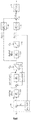
- a scheme of an analog-to-digital converter with dual in-loop quantization according to the present invention is shown in Fig.2 .
- a first quantizer (13) provides a digital output value (Di) of the loop (hence appearing at the end of the forward path).
- This first quantizer may typically have a limited number of bits, e.g. for reducing the complexity associated with error evaluation.
- this first quantizer is in the digital domain and its input is provided by a digital loop filter having a transfer function H d .
- the loop further comprises an analog loop filter having a transfer function H a followed by a second quantizer.
- the second quantizer provides the input of the digital loop filter H d .
- the operation of the quantizers can be modelled as adding a quantization error to the respective quantizer input signal, the quantization error being defined as the difference between the output and the input of the quantizer. Therefore two extra "sources" can be identified in the system, being Q 1 and Q 2 representing the quantization error of the first and second quantizer, respectively.
- Q 1 may be considered a knowable quantity in present system, since both the input and the output of the first quantizer are in the digital domain, and hence these signals can be digitally subtracted to obtain Q 1 .
- Q 2 cannot be determined (without extra measurements) because the input of the second quantizer is an unknown analog signal.
- a classical approach is therefore to consider Q 2 as a source of random noise. With respect to Q 1 , the situation may be different.
- Q 1 Since perfect knowledge of Q 1 can be obtained, it may be possible to compensate the effects caused by it. A key question is of course how to do this and to what extent this is possible when there are uncertainties in the system, such as when one has only imprecise knowledge of the analog filter transfer function H a . If no such compensation is implemented, Q 1 again needs to be treated as a source of random noise that has an impact on the resolution of the overall system.
- the purpose of the A/D converter circuit of the present invention is to largely eliminate the effects of Q 1 .
- Some disclosed embodiments are capable of coping with imprecise knowledge of the analog filter transfer function H a , and even allow adapting to time-varying changes in this filter.
- the two digital outputs D 1 and D 2 in the above system can be determined as a function of the input signal V i and the two quantization error sources Q 1 and Q 2 :
- ⁇ D 1 STF ⁇ V i + NTF ⁇ Q 1 + H d ⁇ NTF ⁇ Q 2
- D 2 STF H d ⁇ V i ⁇ H a ⁇ NTF ⁇ Q 1 + NTF ⁇ Q 2
- STF signal transfer function
- NTF noise transfer function
- the two digital quantizer outputs D 1 and D 2 are filtered by digital filters A(z) and B(z), respectively, and then added.
- the thus obtained recombined output D out can be expressed as : D out z ⁇ A z D 1 z + B z D 2 z
- D out z A z V i + 1 H a z Q 2 Since Q 1 does not appear in the compensated output D out (z), the proposed recombination has completely eliminated the contribution of Q 1 . It is, however, shown later in this description that it is not strictly needed that the ratio of the transfer functions of the digital filters A(z) and B(z) exactly equals H a .
- the first quantizer may have a low resolution (i.e. a low number of bits), because the corresponding quantization error Q 1 can be eliminated in the above explained manner.
- the number of feedback levels may be restricted, which can significantly simplify the design of the error evaluation block.
- a feedback DAC with at most a few bits makes it easier to optimize the system for good linearity.
- a one-bit quantizer can be used.
- the corresponding one-bit feedback DAC is considered inherently linear, because it only has two input-output pairs, which necessarily lie on a straight line.
- a angular sensor is considered which is operated as a tracking loop.
- Fig.3 illustrates such a system.
- the tracking loop in this example contains :
- a delay compensation filter can optionally be provided as well.
- f n represents a normalized frequency that controls the bandwidth of the loop (relative to the sample frequency 1/T).
- the interconnection complexity of the combiner circuit reduces when the number of bits of the angle quantizer is lowered.
- a small number of bits implies a larger angle quantization error, and the strategy to deal with angle quantization error as disclosed in present invention is therefore highly relevant.
- the error evaluation block produces an output signal proportional to the sine of the difference between input angle and the feedback angle corresponding with D 1 . Because sin x ⁇ x for x sufficiently small, the non-linear characteristic can often be neglected when in tracking mode.
- the (total) delay n has been included in the analog filter transfer function H a , while the feedback path and the first quantizer are idealized as having no delay.
- the condition (4) is obviously met.
- the reason why the extra delay z -n is introduced, is to make the filter B(z) physically realizable.
- B z 1 ⁇ z ⁇ 1 K , which represents a realizable FIR filter.
- an optional delay compensation filter may be added to the system whose purpose is to compensate the delay n of the filter A(z).
- Fig.5 One way to realize this filter is shown in Fig.5 .
- a denotes an extra parameter, typically between zero and one, to control the trade-off between overshoot and high-frequency gain (which becomes smaller when a is lowered) on the one hand and on the other hand the settling time (which becomes smaller when a is increased).
- the filter reduces to 1 + n(1-z -1 ), which is an intuitive way for compensating delay based on a 'speed' estimate by differencing the signal, but this choice has a very high overshoot and strongly amplifies high frequencies.
- the input signal transfer function has been changed to the transfer A(z) of the first recombination filter, possibly with the delay thereof being compensated by a delay compensation filter.
- This is particularly interesting for angular sensors which provide an A/D conversion of a possibly fast-changing angle, because it allows improving the dynamic response, e.g. by providing a faster step response.
- Additional digital filtering may be added to any of the exemplary embodiments of present invention, e.g. for increasing the signal-to-noise ratio by reducing the (noise) bandwidth. If such filtering incurs extra delay that cannot be tolerated in the envisioned application, this delay can be compensated, e.g. using the above type of delay compensation filter.
- filters can be designed that provide filtering with near-zero latency, for instance by means of a tracking loop that is completely in the digital domain. Such digital PLL-like structures are known in the art. Also digital counterparts of the tracking loops in the present invention may be used. Note that in all these digital-domain tracking loops the issue of variability is absent, i.e. there are no uncertainties on loop filters, nor mismatch-related nonlinearity problems in the error evaluation block.
- Fig.6 shows an embodiment of the A/D converter according to the invention wherein inner-loop noise shaping is applied.
- the second quantizer Q 2 is embedded in an internal feedback loop, having an analog loop filter with transfer function H b , and a local feedback DAC.
- the dynamics of the local loop is dictated by its signal transfer function H b /(1 + H b ).
- H b z -1 /(1 - z -1 ) this signal transfer function is a simple delay z -1 .
- This simple delay can be directly incorporated in the total delay n of the global feedback loop.
- the delay may also be avoided by adding the optional path shown on the figure. This optional path has the known effect that it makes the signal transfer function of the local loop equal to one.
- the local loop does not alter the dynamic behaviour of the global feedback loop.
- the main effect of the local loop is therefore that it applies noise-shaping to the quantization noise Q 2 of the second quantizer.
- the equivalent quantization noise of the inner loop (which can be considered a quantizer on its own) is Q 2 /(1+H b ).
- An additional advantage of the system with inner-loop noise-shaping is that the non-linearity of the local feedback DAC is suppressed by the global loop. This means that multi-bit DACs can be applied with less stringent conditions on the linearity.
- both quantizers Q 1 and Q 2 operate at the same rate.
- the inner feedback loop around Q 2 and possibly also the digital filter with transfer function H d may be operated at a higher rate compared to the global feedback loop.
- the first quantizer Q 1 then subsamples the digital filter output H d .
- analog filter transfer H a is typically affected by these PVT effects.
- a continuous-time integrator - a particular choice for the analog filter - can easily have a time constant which deviates 30% from its nominal design value.
- Even larger deviations may exist, for instance in certain tracking loops where the overall proportionality factor or gain of the error generation block depends on an amplitude of some input signals, as is for instance the case in a multiplier-based phase detector.
- a tracking loop position/rotation sensor based on sensing the direction of a magnetic field. The strength of the magnetic field may then represent another variable factor affecting the gain of the analog filter transfer H a .
- the condition (4) links two digital filters to an analog transfer function H a . Because the analog transfer function is subject to various sources of variability, the equation is in general not met exactly.
- the signal transfer function A(z) can be chosen more freely compared to the "classical" output D 1 which has a signal transfer function determined by the loop filters. More important for present application are terms in (9) related to Q 1 . From the last term of the above expression, it can be seen that a non-zero ⁇ leads to leakage of Q 1 noise into the compensated output D out . Fortunately, this leaked noise is shaped by NTF(z), which is the noise shaping created by both the analog filter H a and the digital filter H d . When referred to the input, the leaked quantization noise is given by ⁇ (z)NTF(z)/(1+ ⁇ (z)NTF(z))Q 1 .
- recombination filters A(z) and B(z) which result in the analog-to-digital converted output signal D out being less dependent on the quantization noise Q 1 compared to the "classical" output D 1 of the feedback loop.
- the latter may be quantified by comparing the signal-to-noise ratio (SNR) of D out to the SNR of the "classical” output D 1 .
- SNR signal-to-noise ratio
- the recombination filters A(z) and B(z) may be chosen starting from (4) and taking into account the design freedom indicated by (8) and (9), other design procedures are also possible. For instance, one may A(z) and/or B(z) to be parameterized filters, e.g.
- the gain-variability of the analog filter H a is counteracted by introducing a compensating scale factor, for instance in the second recombination filter.
- the second recombination filter (22) comprises a programmable gain G, which allows scaling a signal in accordance with a gain control signal.
- the gain control signal is generated by a gain controller unit (4) which receives the output of the recombiner block (2) and the quantization noise Q 1 .
- the quantization noise Q 1 can for instance be calculated by subtracting the input of the first quantizer from its output, both input and output being signals in the digital domain.
- the gain controller unit (4) comprises filtering means D(z) (41) and E(z) (42) for filtering its input signals, a multiplier (43) for making the product of these filtered signals and an adaptation controller (44) which adapts its output until its input signal becomes on the average zero.
- Equation (9) provides the basis for understanding how the above and other more general adaptive schemes operate.
- ⁇ has on the signal transfer function is disregarded. Note that this approximation is not strictly needed, because the adaptive scheme makes ⁇ small, so the approximation becomes more accurate over time.
- the three terms in (11), corresponding to V i , Q 1 and Q 2 respectively, may be considered statistically uncorrelated.
- a filter D(z) may now be applied to the analog-to-digital converted output signal D out e.g.
- D(z) could be a first order difference 1-z -1 or a second order difference (1-z -1 ) 2 which would largely eliminate the input signal component.
- the filtered output signal i.e. D(z)D out
- eqn. (11) multiplied with D(z).
- E(z) is also a known filter.
- Q 1 is a calculable digital signal, and this can be filtered with the filter E(z).
- the filtered signals D(z)D out and E(z)Q 1 may then be multiplied, as is done in Fig.7 .
- the output of this multiplier provides a measure of the relative mismatch ⁇ (in a statistical sense). This multiplier output may be considered an error signal of the adaptation loop (which is to be minimized).
- the recombination filter A(z) and/or B(z) may be taken as adaptive filter.
- the parameters of the adaptive filter(s) may then be adapted in accordance to methods known in the art for minimizing the error signal, e.g. minimizing this error signal in a mean squared sense.
- a computer program may be stored/distributed on a suitable medium, such as an optical storage medium or a solid-state medium supplied together with or as part of other hardware, but may also be distributed in other forms, such as via the Internet or other wired or wireless telecommunication systems. Any reference signs in the claims should not be construed as limiting the scope.
Landscapes
- Engineering & Computer Science (AREA)
- Theoretical Computer Science (AREA)
- Compression, Expansion, Code Conversion, And Decoders (AREA)
Priority Applications (2)
| Application Number | Priority Date | Filing Date | Title |
|---|---|---|---|
| EP18166658.7A EP3553952B1 (de) | 2018-04-10 | 2018-04-10 | Analog/digital-umsetzer |
| US16/378,794 US10554219B2 (en) | 2018-04-10 | 2019-04-09 | Analog-to-digital converter |
Applications Claiming Priority (1)
| Application Number | Priority Date | Filing Date | Title |
|---|---|---|---|
| EP18166658.7A EP3553952B1 (de) | 2018-04-10 | 2018-04-10 | Analog/digital-umsetzer |
Publications (2)
| Publication Number | Publication Date |
|---|---|
| EP3553952A1 true EP3553952A1 (de) | 2019-10-16 |
| EP3553952B1 EP3553952B1 (de) | 2023-09-13 |
Family
ID=61965813
Family Applications (1)
| Application Number | Title | Priority Date | Filing Date |
|---|---|---|---|
| EP18166658.7A Active EP3553952B1 (de) | 2018-04-10 | 2018-04-10 | Analog/digital-umsetzer |
Country Status (2)
| Country | Link |
|---|---|
| US (1) | US10554219B2 (de) |
| EP (1) | EP3553952B1 (de) |
Cited By (1)
| Publication number | Priority date | Publication date | Assignee | Title |
|---|---|---|---|---|
| EP4170292A1 (de) * | 2021-10-25 | 2023-04-26 | Melexis Technologies SA | Sensorvorrichtung und system mit nichtlinearitätskompensation |
Families Citing this family (2)
| Publication number | Priority date | Publication date | Assignee | Title |
|---|---|---|---|---|
| KR102744050B1 (ko) * | 2020-02-06 | 2024-12-17 | 삼성전자주식회사 | 아날로그 디지털 변환 장치 및 아날로그 디지털 변환 방법 |
| US11349490B2 (en) * | 2020-03-03 | 2022-05-31 | Cirrus Logic, Inc. | Dual-path digital filtering in an analog-to-digital conversion system |
Citations (3)
| Publication number | Priority date | Publication date | Assignee | Title |
|---|---|---|---|---|
| US6313774B1 (en) * | 2000-05-19 | 2001-11-06 | Motorola Inc. | Delta-sigma analog-to-digital converter, and method |
| US6404368B1 (en) * | 1999-09-17 | 2002-06-11 | Nec Corporation | Analog and digital ΔΣ modulator |
| US20110050475A1 (en) | 2009-08-31 | 2011-03-03 | Infineon Technologies Ag | Analog to digital converter with digital filter |
Family Cites Families (6)
| Publication number | Priority date | Publication date | Assignee | Title |
|---|---|---|---|---|
| US4112871A (en) * | 1977-04-14 | 1978-09-12 | New Rochelle Manufacturing Co., Inc. | Bird cage feeder |
| US6920182B2 (en) * | 2001-01-09 | 2005-07-19 | Microtune (Texas), L.P. | Delta-sigma modulator system and method |
| WO2015087476A1 (ja) * | 2013-12-12 | 2015-06-18 | パナソニックIpマネジメント株式会社 | アナログデジタル変換装置、その駆動方法、撮像素子、撮像装置およびバッテリモニタシステム |
| US9397692B1 (en) * | 2015-07-16 | 2016-07-19 | Cirrus Logic International Semiconductor Ltd. | Voltage-controlled oscillator (VCO) as first stage in an analog-to-digital converter (ADC) in combination with a digital filter for second or higher-order noise shaping |
| US9859914B1 (en) * | 2016-08-05 | 2018-01-02 | Mediatek Inc. | Delta-sigma modulator with delta-sigma truncator and associated method for reducing leakage errors of delta-sigma modulator |
| JP6945331B2 (ja) * | 2017-04-18 | 2021-10-06 | ルネサスエレクトロニクス株式会社 | アナログ・ディジタル変換器およびミリ波レーダシステム |
-
2018
- 2018-04-10 EP EP18166658.7A patent/EP3553952B1/de active Active
-
2019
- 2019-04-09 US US16/378,794 patent/US10554219B2/en active Active
Patent Citations (3)
| Publication number | Priority date | Publication date | Assignee | Title |
|---|---|---|---|---|
| US6404368B1 (en) * | 1999-09-17 | 2002-06-11 | Nec Corporation | Analog and digital ΔΣ modulator |
| US6313774B1 (en) * | 2000-05-19 | 2001-11-06 | Motorola Inc. | Delta-sigma analog-to-digital converter, and method |
| US20110050475A1 (en) | 2009-08-31 | 2011-03-03 | Infineon Technologies Ag | Analog to digital converter with digital filter |
Cited By (1)
| Publication number | Priority date | Publication date | Assignee | Title |
|---|---|---|---|---|
| EP4170292A1 (de) * | 2021-10-25 | 2023-04-26 | Melexis Technologies SA | Sensorvorrichtung und system mit nichtlinearitätskompensation |
Also Published As
| Publication number | Publication date |
|---|---|
| EP3553952B1 (de) | 2023-09-13 |
| US20190312584A1 (en) | 2019-10-10 |
| US10554219B2 (en) | 2020-02-04 |
Similar Documents
| Publication | Publication Date | Title |
|---|---|---|
| US12399037B2 (en) | Position sensing device | |
| US8228221B2 (en) | Method and apparatus for calibrating sigma-delta modulator | |
| US9325340B2 (en) | Efficient analog to digital converter | |
| US8803715B2 (en) | Sigma delta modulator including digital to analog coverter (DAC) calibration | |
| JP5696508B2 (ja) | Δς変調器および信号処理システム | |
| US7894536B2 (en) | Calibration model to mitigate data conversion errors | |
| US7821434B2 (en) | Apparatus and method for efficient analog-to-digital conversion | |
| US8970411B2 (en) | Pipelined continuous-time sigma delta modulator | |
| US9843337B1 (en) | Background flash offset calibration in continuous-time delta-sigma ADCS | |
| US5838272A (en) | Error correcting sigma-delta modulation decoding | |
| US8253611B2 (en) | Method for calibrating a pipelined continuous-time sigma delta modulator | |
| CN101416394B (zh) | 用于a/d转换器的校准电路和方法 | |
| JPH06224772A (ja) | マルチビットデルタ−シグマ変調器の較正方法及び装置 | |
| US20200373934A1 (en) | Vco-based continuous-time pipelined adc | |
| JPH0793581B2 (ja) | シグマデルタアナログ/デジタル変換器 | |
| US10554219B2 (en) | Analog-to-digital converter | |
| US7221302B1 (en) | Delta-sigma modulator coefficient calibration method and apparatus | |
| US20090085785A1 (en) | Digital-to-analog converter calibration for multi-bit analog-to-digital converters | |
| KR20180117047A (ko) | 아날로그ㆍ디지털 변환기 및 밀리미터파 레이더 시스템 | |
| JP2004510383A (ja) | シグマ−デルタ・ループおよびフィードバックdacモデルを用いたディジタル−アナログ変換器 | |
| US20100073207A1 (en) | Delta-Sigma Analog-to-Digital Converters and Methods to Calibrate Delta-Sigma Analog-to-Digital Converters | |
| US9906237B1 (en) | Digital-to-analog converter and method of operating | |
| US9246509B1 (en) | Methods and apparatus for offline mismatch removal in sigma delta analog-to-digital converters | |
| JP5286420B2 (ja) | アナログデジタル変換器およびそれを用いた半導体集積回路装置 | |
| Rutten et al. | Digital calibration of a continuous-time cascaded ΣΔ modulator based on variance derivative estimation |
Legal Events
| Date | Code | Title | Description |
|---|---|---|---|
| PUAI | Public reference made under article 153(3) epc to a published international application that has entered the european phase |
Free format text: ORIGINAL CODE: 0009012 |
|
| STAA | Information on the status of an ep patent application or granted ep patent |
Free format text: STATUS: THE APPLICATION HAS BEEN PUBLISHED |
|
| AK | Designated contracting states |
Kind code of ref document: A1 Designated state(s): AL AT BE BG CH CY CZ DE DK EE ES FI FR GB GR HR HU IE IS IT LI LT LU LV MC MK MT NL NO PL PT RO RS SE SI SK SM TR |
|
| AX | Request for extension of the european patent |
Extension state: BA ME |
|
| STAA | Information on the status of an ep patent application or granted ep patent |
Free format text: STATUS: REQUEST FOR EXAMINATION WAS MADE |
|
| 17P | Request for examination filed |
Effective date: 20191220 |
|
| RBV | Designated contracting states (corrected) |
Designated state(s): AL AT BE BG CH CY CZ DE DK EE ES FI FR GB GR HR HU IE IS IT LI LT LU LV MC MK MT NL NO PL PT RO RS SE SI SK SM TR |
|
| STAA | Information on the status of an ep patent application or granted ep patent |
Free format text: STATUS: EXAMINATION IS IN PROGRESS |
|
| 17Q | First examination report despatched |
Effective date: 20201120 |
|
| GRAP | Despatch of communication of intention to grant a patent |
Free format text: ORIGINAL CODE: EPIDOSNIGR1 |
|
| STAA | Information on the status of an ep patent application or granted ep patent |
Free format text: STATUS: GRANT OF PATENT IS INTENDED |
|
| INTG | Intention to grant announced |
Effective date: 20230322 |
|
| GRAS | Grant fee paid |
Free format text: ORIGINAL CODE: EPIDOSNIGR3 |
|
| GRAA | (expected) grant |
Free format text: ORIGINAL CODE: 0009210 |
|
| STAA | Information on the status of an ep patent application or granted ep patent |
Free format text: STATUS: THE PATENT HAS BEEN GRANTED |
|
| AK | Designated contracting states |
Kind code of ref document: B1 Designated state(s): AL AT BE BG CH CY CZ DE DK EE ES FI FR GB GR HR HU IE IS IT LI LT LU LV MC MK MT NL NO PL PT RO RS SE SI SK SM TR |
|
| REG | Reference to a national code |
Ref country code: GB Ref legal event code: FG4D |
|
| REG | Reference to a national code |
Ref country code: CH Ref legal event code: EP |
|
| REG | Reference to a national code |
Ref country code: DE Ref legal event code: R096 Ref document number: 602018057368 Country of ref document: DE |
|
| REG | Reference to a national code |
Ref country code: IE Ref legal event code: FG4D |
|
| P01 | Opt-out of the competence of the unified patent court (upc) registered |
Effective date: 20231109 |
|
| REG | Reference to a national code |
Ref country code: LT Ref legal event code: MG9D |
|
| REG | Reference to a national code |
Ref country code: NL Ref legal event code: MP Effective date: 20230913 |
|
| PG25 | Lapsed in a contracting state [announced via postgrant information from national office to epo] |
Ref country code: GR Free format text: LAPSE BECAUSE OF FAILURE TO SUBMIT A TRANSLATION OF THE DESCRIPTION OR TO PAY THE FEE WITHIN THE PRESCRIBED TIME-LIMIT Effective date: 20231214 |
|
| PG25 | Lapsed in a contracting state [announced via postgrant information from national office to epo] |
Ref country code: SE Free format text: LAPSE BECAUSE OF FAILURE TO SUBMIT A TRANSLATION OF THE DESCRIPTION OR TO PAY THE FEE WITHIN THE PRESCRIBED TIME-LIMIT Effective date: 20230913 Ref country code: RS Free format text: LAPSE BECAUSE OF FAILURE TO SUBMIT A TRANSLATION OF THE DESCRIPTION OR TO PAY THE FEE WITHIN THE PRESCRIBED TIME-LIMIT Effective date: 20230913 Ref country code: NO Free format text: LAPSE BECAUSE OF FAILURE TO SUBMIT A TRANSLATION OF THE DESCRIPTION OR TO PAY THE FEE WITHIN THE PRESCRIBED TIME-LIMIT Effective date: 20231213 Ref country code: LV Free format text: LAPSE BECAUSE OF FAILURE TO SUBMIT A TRANSLATION OF THE DESCRIPTION OR TO PAY THE FEE WITHIN THE PRESCRIBED TIME-LIMIT Effective date: 20230913 Ref country code: LT Free format text: LAPSE BECAUSE OF FAILURE TO SUBMIT A TRANSLATION OF THE DESCRIPTION OR TO PAY THE FEE WITHIN THE PRESCRIBED TIME-LIMIT Effective date: 20230913 Ref country code: HR Free format text: LAPSE BECAUSE OF FAILURE TO SUBMIT A TRANSLATION OF THE DESCRIPTION OR TO PAY THE FEE WITHIN THE PRESCRIBED TIME-LIMIT Effective date: 20230913 Ref country code: GR Free format text: LAPSE BECAUSE OF FAILURE TO SUBMIT A TRANSLATION OF THE DESCRIPTION OR TO PAY THE FEE WITHIN THE PRESCRIBED TIME-LIMIT Effective date: 20231214 Ref country code: FI Free format text: LAPSE BECAUSE OF FAILURE TO SUBMIT A TRANSLATION OF THE DESCRIPTION OR TO PAY THE FEE WITHIN THE PRESCRIBED TIME-LIMIT Effective date: 20230913 |
|
| REG | Reference to a national code |
Ref country code: AT Ref legal event code: MK05 Ref document number: 1612323 Country of ref document: AT Kind code of ref document: T Effective date: 20230913 |
|
| PG25 | Lapsed in a contracting state [announced via postgrant information from national office to epo] |
Ref country code: NL Free format text: LAPSE BECAUSE OF FAILURE TO SUBMIT A TRANSLATION OF THE DESCRIPTION OR TO PAY THE FEE WITHIN THE PRESCRIBED TIME-LIMIT Effective date: 20230913 |
|
| PG25 | Lapsed in a contracting state [announced via postgrant information from national office to epo] |
Ref country code: IS Free format text: LAPSE BECAUSE OF FAILURE TO SUBMIT A TRANSLATION OF THE DESCRIPTION OR TO PAY THE FEE WITHIN THE PRESCRIBED TIME-LIMIT Effective date: 20240113 |
|
| PG25 | Lapsed in a contracting state [announced via postgrant information from national office to epo] |
Ref country code: AT Free format text: LAPSE BECAUSE OF FAILURE TO SUBMIT A TRANSLATION OF THE DESCRIPTION OR TO PAY THE FEE WITHIN THE PRESCRIBED TIME-LIMIT Effective date: 20230913 |
|
| PG25 | Lapsed in a contracting state [announced via postgrant information from national office to epo] |
Ref country code: ES Free format text: LAPSE BECAUSE OF FAILURE TO SUBMIT A TRANSLATION OF THE DESCRIPTION OR TO PAY THE FEE WITHIN THE PRESCRIBED TIME-LIMIT Effective date: 20230913 |
|
| PG25 | Lapsed in a contracting state [announced via postgrant information from national office to epo] |
Ref country code: SM Free format text: LAPSE BECAUSE OF FAILURE TO SUBMIT A TRANSLATION OF THE DESCRIPTION OR TO PAY THE FEE WITHIN THE PRESCRIBED TIME-LIMIT Effective date: 20230913 Ref country code: RO Free format text: LAPSE BECAUSE OF FAILURE TO SUBMIT A TRANSLATION OF THE DESCRIPTION OR TO PAY THE FEE WITHIN THE PRESCRIBED TIME-LIMIT Effective date: 20230913 Ref country code: IS Free format text: LAPSE BECAUSE OF FAILURE TO SUBMIT A TRANSLATION OF THE DESCRIPTION OR TO PAY THE FEE WITHIN THE PRESCRIBED TIME-LIMIT Effective date: 20240113 Ref country code: ES Free format text: LAPSE BECAUSE OF FAILURE TO SUBMIT A TRANSLATION OF THE DESCRIPTION OR TO PAY THE FEE WITHIN THE PRESCRIBED TIME-LIMIT Effective date: 20230913 Ref country code: EE Free format text: LAPSE BECAUSE OF FAILURE TO SUBMIT A TRANSLATION OF THE DESCRIPTION OR TO PAY THE FEE WITHIN THE PRESCRIBED TIME-LIMIT Effective date: 20230913 Ref country code: CZ Free format text: LAPSE BECAUSE OF FAILURE TO SUBMIT A TRANSLATION OF THE DESCRIPTION OR TO PAY THE FEE WITHIN THE PRESCRIBED TIME-LIMIT Effective date: 20230913 Ref country code: AT Free format text: LAPSE BECAUSE OF FAILURE TO SUBMIT A TRANSLATION OF THE DESCRIPTION OR TO PAY THE FEE WITHIN THE PRESCRIBED TIME-LIMIT Effective date: 20230913 Ref country code: SK Free format text: LAPSE BECAUSE OF FAILURE TO SUBMIT A TRANSLATION OF THE DESCRIPTION OR TO PAY THE FEE WITHIN THE PRESCRIBED TIME-LIMIT Effective date: 20230913 Ref country code: PT Free format text: LAPSE BECAUSE OF FAILURE TO SUBMIT A TRANSLATION OF THE DESCRIPTION OR TO PAY THE FEE WITHIN THE PRESCRIBED TIME-LIMIT Effective date: 20240115 |
|
| PG25 | Lapsed in a contracting state [announced via postgrant information from national office to epo] |
Ref country code: PL Free format text: LAPSE BECAUSE OF FAILURE TO SUBMIT A TRANSLATION OF THE DESCRIPTION OR TO PAY THE FEE WITHIN THE PRESCRIBED TIME-LIMIT Effective date: 20230913 Ref country code: IT Free format text: LAPSE BECAUSE OF FAILURE TO SUBMIT A TRANSLATION OF THE DESCRIPTION OR TO PAY THE FEE WITHIN THE PRESCRIBED TIME-LIMIT Effective date: 20230913 |
|
| REG | Reference to a national code |
Ref country code: DE Ref legal event code: R097 Ref document number: 602018057368 Country of ref document: DE |
|
| PG25 | Lapsed in a contracting state [announced via postgrant information from national office to epo] |
Ref country code: DK Free format text: LAPSE BECAUSE OF FAILURE TO SUBMIT A TRANSLATION OF THE DESCRIPTION OR TO PAY THE FEE WITHIN THE PRESCRIBED TIME-LIMIT Effective date: 20230913 |
|
| PLBE | No opposition filed within time limit |
Free format text: ORIGINAL CODE: 0009261 |
|
| STAA | Information on the status of an ep patent application or granted ep patent |
Free format text: STATUS: NO OPPOSITION FILED WITHIN TIME LIMIT |
|
| PG25 | Lapsed in a contracting state [announced via postgrant information from national office to epo] |
Ref country code: DK Free format text: LAPSE BECAUSE OF FAILURE TO SUBMIT A TRANSLATION OF THE DESCRIPTION OR TO PAY THE FEE WITHIN THE PRESCRIBED TIME-LIMIT Effective date: 20230913 |
|
| 26N | No opposition filed |
Effective date: 20240614 |
|
| PG25 | Lapsed in a contracting state [announced via postgrant information from national office to epo] |
Ref country code: SI Free format text: LAPSE BECAUSE OF FAILURE TO SUBMIT A TRANSLATION OF THE DESCRIPTION OR TO PAY THE FEE WITHIN THE PRESCRIBED TIME-LIMIT Effective date: 20230913 |
|
| PG25 | Lapsed in a contracting state [announced via postgrant information from national office to epo] |
Ref country code: SI Free format text: LAPSE BECAUSE OF FAILURE TO SUBMIT A TRANSLATION OF THE DESCRIPTION OR TO PAY THE FEE WITHIN THE PRESCRIBED TIME-LIMIT Effective date: 20230913 |
|
| PG25 | Lapsed in a contracting state [announced via postgrant information from national office to epo] |
Ref country code: BG Free format text: LAPSE BECAUSE OF FAILURE TO SUBMIT A TRANSLATION OF THE DESCRIPTION OR TO PAY THE FEE WITHIN THE PRESCRIBED TIME-LIMIT Effective date: 20230913 |
|
| PG25 | Lapsed in a contracting state [announced via postgrant information from national office to epo] |
Ref country code: MC Free format text: LAPSE BECAUSE OF FAILURE TO SUBMIT A TRANSLATION OF THE DESCRIPTION OR TO PAY THE FEE WITHIN THE PRESCRIBED TIME-LIMIT Effective date: 20230913 |
|
| PG25 | Lapsed in a contracting state [announced via postgrant information from national office to epo] |
Ref country code: MC Free format text: LAPSE BECAUSE OF FAILURE TO SUBMIT A TRANSLATION OF THE DESCRIPTION OR TO PAY THE FEE WITHIN THE PRESCRIBED TIME-LIMIT Effective date: 20230913 Ref country code: BG Free format text: LAPSE BECAUSE OF FAILURE TO SUBMIT A TRANSLATION OF THE DESCRIPTION OR TO PAY THE FEE WITHIN THE PRESCRIBED TIME-LIMIT Effective date: 20230913 |
|
| REG | Reference to a national code |
Ref country code: CH Ref legal event code: PL |
|
| PG25 | Lapsed in a contracting state [announced via postgrant information from national office to epo] |
Ref country code: LU Free format text: LAPSE BECAUSE OF NON-PAYMENT OF DUE FEES Effective date: 20240410 |
|
| GBPC | Gb: european patent ceased through non-payment of renewal fee |
Effective date: 20240410 |
|
| REG | Reference to a national code |
Ref country code: BE Ref legal event code: MM Effective date: 20240430 |
|
| PG25 | Lapsed in a contracting state [announced via postgrant information from national office to epo] |
Ref country code: LU Free format text: LAPSE BECAUSE OF NON-PAYMENT OF DUE FEES Effective date: 20240410 |
|
| PG25 | Lapsed in a contracting state [announced via postgrant information from national office to epo] |
Ref country code: BE Free format text: LAPSE BECAUSE OF NON-PAYMENT OF DUE FEES Effective date: 20240430 |
|
| PG25 | Lapsed in a contracting state [announced via postgrant information from national office to epo] |
Ref country code: GB Free format text: LAPSE BECAUSE OF NON-PAYMENT OF DUE FEES Effective date: 20240410 |
|
| PG25 | Lapsed in a contracting state [announced via postgrant information from national office to epo] |
Ref country code: GB Free format text: LAPSE BECAUSE OF NON-PAYMENT OF DUE FEES Effective date: 20240410 Ref country code: BE Free format text: LAPSE BECAUSE OF NON-PAYMENT OF DUE FEES Effective date: 20240430 Ref country code: CH Free format text: LAPSE BECAUSE OF NON-PAYMENT OF DUE FEES Effective date: 20240430 |
|
| PG25 | Lapsed in a contracting state [announced via postgrant information from national office to epo] |
Ref country code: IE Free format text: LAPSE BECAUSE OF NON-PAYMENT OF DUE FEES Effective date: 20240410 |
|
| PGFP | Annual fee paid to national office [announced via postgrant information from national office to epo] |
Ref country code: DE Payment date: 20250319 Year of fee payment: 8 |
|
| PG25 | Lapsed in a contracting state [announced via postgrant information from national office to epo] |
Ref country code: CY Free format text: LAPSE BECAUSE OF FAILURE TO SUBMIT A TRANSLATION OF THE DESCRIPTION OR TO PAY THE FEE WITHIN THE PRESCRIBED TIME-LIMIT; INVALID AB INITIO Effective date: 20180410 |
|
| PG25 | Lapsed in a contracting state [announced via postgrant information from national office to epo] |
Ref country code: HU Free format text: LAPSE BECAUSE OF FAILURE TO SUBMIT A TRANSLATION OF THE DESCRIPTION OR TO PAY THE FEE WITHIN THE PRESCRIBED TIME-LIMIT; INVALID AB INITIO Effective date: 20180410 |
|
| PGFP | Annual fee paid to national office [announced via postgrant information from national office to epo] |
Ref country code: FR Payment date: 20260320 Year of fee payment: 9 |