EP3553665A1 - Zugangsverfahren, -vorrichtung und -system für nichtflüchtigen speicher - Google Patents
Zugangsverfahren, -vorrichtung und -system für nichtflüchtigen speicher Download PDFInfo
- Publication number
- EP3553665A1 EP3553665A1 EP16925965.2A EP16925965A EP3553665A1 EP 3553665 A1 EP3553665 A1 EP 3553665A1 EP 16925965 A EP16925965 A EP 16925965A EP 3553665 A1 EP3553665 A1 EP 3553665A1
- Authority
- EP
- European Patent Office
- Prior art keywords
- address information
- page table
- ait
- address
- nvm
- Prior art date
- Legal status (The legal status is an assumption and is not a legal conclusion. Google has not performed a legal analysis and makes no representation as to the accuracy of the status listed.)
- Granted
Links
Images
Classifications
-
- G—PHYSICS
- G06—COMPUTING OR CALCULATING; COUNTING
- G06F—ELECTRIC DIGITAL DATA PROCESSING
- G06F12/00—Accessing, addressing or allocating within memory systems or architectures
- G06F12/02—Addressing or allocation; Relocation
- G06F12/08—Addressing or allocation; Relocation in hierarchically structured memory systems, e.g. virtual memory systems
- G06F12/0802—Addressing of a memory level in which the access to the desired data or data block requires associative addressing means, e.g. caches
- G06F12/0862—Addressing of a memory level in which the access to the desired data or data block requires associative addressing means, e.g. caches with prefetch
-
- G—PHYSICS
- G06—COMPUTING OR CALCULATING; COUNTING
- G06F—ELECTRIC DIGITAL DATA PROCESSING
- G06F12/00—Accessing, addressing or allocating within memory systems or architectures
- G06F12/02—Addressing or allocation; Relocation
- G06F12/0223—User address space allocation, e.g. contiguous or non contiguous base addressing
- G06F12/023—Free address space management
- G06F12/0238—Memory management in non-volatile memory, e.g. resistive RAM or ferroelectric memory
-
- G—PHYSICS
- G06—COMPUTING OR CALCULATING; COUNTING
- G06F—ELECTRIC DIGITAL DATA PROCESSING
- G06F12/00—Accessing, addressing or allocating within memory systems or architectures
- G06F12/02—Addressing or allocation; Relocation
- G06F12/08—Addressing or allocation; Relocation in hierarchically structured memory systems, e.g. virtual memory systems
- G06F12/0802—Addressing of a memory level in which the access to the desired data or data block requires associative addressing means, e.g. caches
- G06F12/0806—Multiuser, multiprocessor or multiprocessing cache systems
- G06F12/0815—Cache consistency protocols
- G06F12/0831—Cache consistency protocols using a bus scheme, e.g. with bus monitoring or watching means
-
- G—PHYSICS
- G06—COMPUTING OR CALCULATING; COUNTING
- G06F—ELECTRIC DIGITAL DATA PROCESSING
- G06F12/00—Accessing, addressing or allocating within memory systems or architectures
- G06F12/02—Addressing or allocation; Relocation
- G06F12/08—Addressing or allocation; Relocation in hierarchically structured memory systems, e.g. virtual memory systems
- G06F12/10—Address translation
- G06F12/1009—Address translation using page tables, e.g. page table structures
-
- G—PHYSICS
- G06—COMPUTING OR CALCULATING; COUNTING
- G06F—ELECTRIC DIGITAL DATA PROCESSING
- G06F12/00—Accessing, addressing or allocating within memory systems or architectures
- G06F12/02—Addressing or allocation; Relocation
- G06F12/08—Addressing or allocation; Relocation in hierarchically structured memory systems, e.g. virtual memory systems
- G06F12/10—Address translation
- G06F12/1027—Address translation using associative or pseudo-associative address translation means, e.g. translation look-aside buffer [TLB]
- G06F12/1045—Address translation using associative or pseudo-associative address translation means, e.g. translation look-aside buffer [TLB] associated with a data cache
- G06F12/1054—Address translation using associative or pseudo-associative address translation means, e.g. translation look-aside buffer [TLB] associated with a data cache the data cache being concurrently physically addressed
-
- G—PHYSICS
- G06—COMPUTING OR CALCULATING; COUNTING
- G06F—ELECTRIC DIGITAL DATA PROCESSING
- G06F2212/00—Indexing scheme relating to accessing, addressing or allocation within memory systems or architectures
- G06F2212/10—Providing a specific technical effect
- G06F2212/1016—Performance improvement
- G06F2212/1021—Hit rate improvement
-
- G—PHYSICS
- G06—COMPUTING OR CALCULATING; COUNTING
- G06F—ELECTRIC DIGITAL DATA PROCESSING
- G06F2212/00—Indexing scheme relating to accessing, addressing or allocation within memory systems or architectures
- G06F2212/20—Employing a main memory using a specific memory technology
- G06F2212/202—Non-volatile memory
-
- G—PHYSICS
- G06—COMPUTING OR CALCULATING; COUNTING
- G06F—ELECTRIC DIGITAL DATA PROCESSING
- G06F2212/00—Indexing scheme relating to accessing, addressing or allocation within memory systems or architectures
- G06F2212/65—Details of virtual memory and virtual address translation
- G06F2212/651—Multi-level translation tables
-
- G—PHYSICS
- G06—COMPUTING OR CALCULATING; COUNTING
- G06F—ELECTRIC DIGITAL DATA PROCESSING
- G06F2212/00—Indexing scheme relating to accessing, addressing or allocation within memory systems or architectures
- G06F2212/72—Details relating to flash memory management
- G06F2212/7201—Logical to physical mapping or translation of blocks or pages
Definitions
- Embodiments of the present invention relate to the field of computers, and in particular, to a method, an apparatus, and a system for accessing a non-volatile memory.
- a memory of a host is always an important constituent part of a computer system, and is an important part that decides performance of the system.
- a conventional memory always includes a dynamic random access memory (Dynamic Random Access Memory, DRAM).
- DRAM Dynamic Random Access Memory
- a biggest disadvantage of the memory including the DRAM is that the memory is volatile. data stored in the memory DRAM is lost when the host is powered off, leading to unrecoverable data loss. This poses a great challenge to consistency and reliability of the data.
- an additional complex data power-off protection measure usually needs to be used.
- the DRAM needs to perform a data refresh operation at particular intervals to avoid data loss. This directly leads to extremely high power consumption of the DRAM.
- Non-volatile memories such as a phase change memory (Phase change memory, PCM), a magnetoresistive random-access memory (Magnetoresistive Random-Access Memory, MRAM), a ferroelectric memory (Ferro electronic RAM, Fe RAM), and a flash memory gradually become a trend.
- the NVM has advantages such as being non-volatile when power is off, and having high storage density, no need to frequently refresh, and low power consumption.
- an access technology for the NVM is not mature.
- TLB translation look aside buffer
- the present invention discloses a method, an apparatus, and a system for accessing a non-volatile memory (Non-Volatile Memory, NVM), to reduce a memory access delay by prefetching a to-be-accessed address indirection table (Address Indirection Table, AIT) entry to an AIT cache.
- NVM Non-Volatile Memory
- AIT Address Indirection Table
- this application discloses a method for accessing a non-volatile memory.
- the method includes: receiving, by an NVM controller, a first access request from a processor; determining, based on first address information carried in the first access request, whether the first access request is used to access a page table; and if the first access request is used to access the page table, reading, by the NVM controller, a page table entry indicated by the first address information, obtaining, based on second address information recorded in the page table entry, an AIT entry corresponding to the second address information from an AIT, and caching the AIT entry to an AIT cache.
- the second address information may be a physical page number, used to indicate a physical page to be accessed by the processor.
- the AIT is used to record a mapping relationship between a physical address and an NVM device address. More specifically, the AIT is used to record a mapping relationship between a physical block number and an NVM inner block number.
- the NVM controller monitors access to the page table. If an AIT entry corresponding to a physical page number recorded by an accessed page table entry does not exist in the AIT cache, the NMV controller prefetches one or more AIT entries corresponding to the physical page number, and caches the one or more AIT entries to the AIT cache. Subsequently, the NVM may directly obtain, from the AIT cache, an NVM inner block number corresponding to a to-be-accessed physical block number.
- the method further includes: sending, by the NVM controller, the second address information to the processor; receiving a second access request from the processor, where the second access request carries the second address information; and obtaining, by the NVM controller based on the second address information and the AIT entry in the AIT cache, an NVM device address corresponding to the second address information, and accessing the NVM based on the NVM device address corresponding to the second address information.
- the second access request carries third address information.
- a partial field of the third address information is the second address information.
- the third address information is a physical address to be accessed by the processor, and the second address information is a physical page number.
- the NVM device address corresponding to the second address information is an NVM inner block number.
- the NVM controller obtains, based on the physical page number and the AIT entry in the AIT cache, an NVM inner block number corresponding to the physical page number, and accesses the NVM based on the NVM inner block number and a partial field of the third address information.
- the method further includes: determining, by the NVM controller based on the second address information, whether the second access request is used to access the page table; and if the second access request is used to access the page table, deleting, by the NVM controller, the AIT entry corresponding to the second address information from the AIT cache after obtaining the NVM device address corresponding to the second address information.
- both the first access request and the second access request are used to access the page table, it indicates that the page table is a multi-level page table.
- a final correspondence between a virtual page number and the physical page number is cached in a TLB, so that reusability of the previously cached AIT entry is not high.
- the AIT entry corresponding to the second address information may be deleted from the AIT cache. It should be understood that deletion herein may be invalidating the page table entry or replacing the page table entry in next cache replacement.
- the method before the determining, by the NVM controller, whether the access request is used to access a page table entry, the method further includes: receiving, by the NVM controller, page table address information from the processor. The NVM controller determines, based on the first address information and the page table address information, whether the first access request is used to access the page table.
- the page table address information includes a page table base address and a page table size.
- the NVM controller may determine an address range of the page table based on the page table base address and the page table size.
- the NVM controller may determine whether the first access request is used to access the page table by determining whether the first address information falls within the address range of the page table.
- the method further includes: receiving, by the NVM controller, page table invalidity information from the processor, and invalidating the page table address information based on the page table invalidity information.
- the processor After destructing a process, the processor sends a page table invalidity message to the NVM controller. After receiving the page table invalidity message from the processor, the NVM controller invalidates page table address information related to the process. In this way, a storage space on an NVM controller side is saved.
- this application provides a readable medium, including an execution instruction.
- a processor of a storage controller executes the execution instruction, the storage controller performs the method according to any one of the first aspect or the possible implementations of the first aspect.
- this application provides an NVM storage controller, including a processor, a memory, and a bus.
- the memory is configured to store an execution instruction.
- the processor and the memory are connected by using the bus.
- the processor executes the execution instruction stored in the memory, so that the NVM storage controller performs the method according to any one of the first aspect or the possible implementations of the first aspect.
- this application provides an apparatus for accessing a non-volatile memory.
- the apparatus includes: a receiving unit, configured to receive a first access request from a processor, where the first access request carries first address information; a determining unit, configured to determine, based on the first address information, whether the first access request is used to access a page table; and a processing unit, where if the first access request is used to access the page table, the processing unit is configured to: read a page table entry indicated by the first address information, obtain, based on second address information recorded in the page table entry, an AIT entry corresponding to the second address information from an address indirection table AIT, and cache the AIT entry to an AIT cache, where the AIT is used to record a mapping relationship between a physical address and an NVM device address.
- the apparatus further includes a sending unit, configured to send the second address information to the processor.
- the receiving unit is further configured to receive a second access request from the processor, where the second access request carries the second address information.
- the processing unit is further configured to: obtain, based on the second address information and the AIT entry in the AIT cache, an NVM device address corresponding to the second address information, and access the NVM based on the NVM device address corresponding to the second address information.
- the determining unit is further configured to determine, based on the second address information, whether the second access request is used to access the page table; and if the second access request is used to access the page table, the processing unit is further configured to delete the AIT entry from the AIT cache after obtaining the NVM device address corresponding to the second address information.
- the receiving unit is further configured to receive page table address information from the processor; and the determining unit is configured to determine, based on the first address information and the page table address information, whether the first access request is used to access the page table.
- the receiving unit is further configured to receive page table invalidity information from the processor; and the processing unit is further configured to invalidate the page table address information based on the page table invalidity information.
- the fourth aspect provides apparatus implementations corresponding to the method according to the first aspect, so that descriptions according to any one of the first aspect or the possible implementations of the first aspect are correspondingly applicable to any one of the fourth aspect or the possible implementations of the fourth aspect. Details are not described herein again.
- this application provides a system for accessing a non-volatile memory.
- the system includes a processor, a non-volatile memory NVM, and the apparatus for accessing a non-volatile memory according to any one of fourth aspect or the possible implementations of the fourth aspect.
- the NVM controller monitors access of the processor to the page table.
- the NVM controller parses content of the page table to obtain a physical page number that may be subsequently accessed, prefetches an AIT entry corresponding to the physical page number from the AIT in advance before the processor really accesses the physical page number, and caches the prefetched AIT entry to the AIT cache. In this way, subsequent AIT cache misses are reduced, thereby increasing a data access speed of the NVM.
- a system application uses a virtual address of a memory.
- a processor needs to map the virtual address to a physical address. More specifically, the processor needs to convert a virtual page number in the virtual address into a physical page number.
- a page table stores the physical page number corresponding to the virtual page number. The processor may index, in the page table based on the virtual address (or a partial field of the virtual address), the physical page number corresponding to the virtual page number.
- the page table is usually stored in the memory, and access to the page table once needs access to the memory once.
- the processor caches some frequently-used mapping relationships between virtual page numbers and physical page numbers by using a translation lookaside buffer (translation look aside buffer, TLB).
- TLB translation look aside buffer
- an access request sent by a processor to an NVM controller carries a to-be-accessed physical address.
- the NVM controller further needs to convert the to-be-accessed physical address into an actual NVM device address, and performs memory access based on the NVM device address. More specifically, the NVM controller performs management and mapping on a physical address space and an NVM device address space in units of blocks.
- the NVM controller needs to convert a physical block number in the physical address into an NVM inner block number.
- An address indirection table (Address Indirection Table, AIT) stores a correspondence between the physical block number and the NVM inner block number.
- the NVM controller may index, in the AIT based on the physical address (or a partial field of the physical address), the NVM inner block number corresponding to the physical block number.
- a mapping relationship between the physical address and the NVM device address may be specifically a mapping relationship between the physical block number and the NVM inner block number.
- the NVM controller uses an AIT cache to cache some frequently-used mapping relationships between physical addresses and NVM device addresses.
- an AIT cache hit occurs.
- an AIT cache miss occurs. In this case, the NVM controller needs to query the AIT for the NVM device address corresponding to the physical address.
- the NVM controller listens to an access event of the processor for the page table. When listening and detecting that the processor is to access the page table, the NVM controller determines, based on a page table entry accessed by the processor, a to-be-accessed physical page number. If an NVM inner block number corresponding to a to-be-accessed physical page does not exist in the AIT cache, the NVM controller determines an AIT entry corresponding to the to-be-accessed physical page number, and caches the AIT entry to the AIT cache.
- the NVM controller determines an AIT entry corresponding to a physical block in which the to-be-accessed physical page is located, and caches the AIT entry to the AIT cache.
- the AIT entry records a mapping relationship between the physical block number and the NVM inner block number. In this way, subsequent AIT cache misses are reduced or avoided, thereby reducing a memory access delay of the NVM.
- a virtual address, a physical address, and an NVM device address are used to describe a plurality of solutions.
- the virtual address may be a partial field of an actual virtual address
- the physical address may be a partial field of an actual physical address
- the NVM device address may also be a partial field of an actual NVM device address.
- a virtual page number is a partial field of the virtual address
- a physical page number is a partial field of the physical address
- a physical block number is also a partial field of the physical address
- an NVM inner block number is a partial field of the NVM device address.
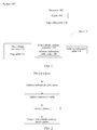
- FIG. 1 is a schematic diagram of a logical structure of a system 100 according to an embodiment of the present invention.
- the system 100 includes a processor 102, a cache 104, a page table cache 106, an address indirection table cache 108, a non-volatile memory controller 110, a non-volatile memory 112, an address indirection table 114, a page table 116, and a bus 118.
- the page table 116 stores a physical page number corresponding to a virtual page number of the system.
- the page table cache 106 stores a mapping relationship that is between a virtual page number and a physical page number and that is frequently used by the system.
- the page table cache 106 may be configured inside or outside the processor 102, and is connected to the processor 102 by using the bus 118.
- the address indirection table 114 stores a mapping relationship between a physical address of the system and an NVM device address.
- the AIT 114 may be stored in a storage space independent of the non-volatile memory 112 and is not transparent to the processor 102.
- the AIT 114 may be stored in a dynamic random access memory (Dynamic Random Access Memory, DRAM) mounted on the NVM controller 110.
- DRAM Dynamic Random Access Memory
- this embodiment of the present invention does not limit a storage form of the AIT 114.
- the AIT 114 is directly stored in an independent storage space in the NVM 112.
- the address indirection table cache 108 stores a mapping relationship that is between a physical address and an NVM device address and that is frequently used by the system. Data stored in the address indirection table cache 108 is a subset of data stored in the address indirection table 114.
- mapping relationship that is between a physical address and an NVM device address and that is stored in the AIT 114 or the AIT cache 108 is a mapping relationship between a physical block number and an NVM inner block number.
- the processor 102 may include one or more processor cores, and is configured to execute a computer program instruction of the system 100.
- the processor 102 may be specifically implemented in a form of a general central processing unit (Central Processing Unit, CPU), a microprocessor, an application-specific integrated circuit (Application Specific Integrated Circuit, ASIC), one or more integrated circuits, or the like.
- CPU Central Processing Unit
- ASIC Application Specific Integrated Circuit
- a component for example, the processor 102, configured to perform a particular function may be implemented by configuring a general component to perform a corresponding function or by using a dedicated component for specially performing the particular function. This is not limited in this application.
- the cache 104 may include a one-level or multi-level cache.
- the cache 104 may include a one-level (L0) cache and a two-level (LI) cache.
- the non-volatile memory controller 110 is configured to process an access operation on the NVM 112.
- the memory controller may be specifically implemented in a form of a general processor, a microprocessor, an application-specific integrated circuit, one or more integrated circuits, or the like.
- the non-volatile memory 112 may be directly connected to the non-volatile memory controller 110, as shown in FIG. 1 , or may be directly connected to the bus 110 and is connected to the non-volatile memory controller 110 by using the bus 110. This is not limited in this embodiment of the present invention.
- a request for example, memory reading, memory writing, or prefetching, related to memory access and generated by the processor 102 is executed by the non-volatile memory controller 110.
- the processor 102 runs a memory access instruction, it is first queried whether a physical address corresponding to a virtual address to be accessed according to the memory access instruction is included in the TLB 106. If a mapping relationship between the virtual address to be accessed according to the memory access instruction and the physical address is found in the TLB 106, a TLB hit occurs, and a memory access request in which the to-be-accessed physical address is included is transmitted. If a TLB miss occurs, the processor needs to search the page table 116 for a physical page number corresponding to a to-be-accessed virtual page number.
- mapping relationships between physical addresses and NVM device addresses are maintained in the AIT cache 108.
- the NVM controller 110 After receiving the access request of the processor 102, the NVM controller 110 first searches the AIT cache 108 for a mapping relationship between the to-be-accessed physical address and an NVM device address. If an AIT cache hit occurs, the NVM controller 110 accesses the NVM memory 112 based on the obtained NVM device address. If an AIT miss occurs, the NVM controller 110 needs to query the AIT 114 to obtain the mapping relationship between the to-be-accessed physical address and the NVM device address.
- the NVM controller 110 After receiving the access request sent by the processor 102, the NVM controller 110 first searches the AIT cache 108 for an NVM inner block number corresponding to a physical block number. If the AIT cache hit occurs, after determining the NVM device address based on the NVM inner block number and a partial field of address information carried in the access request, the NVM adds the access request to an NVM access queue. If the AIT cache miss occurs, the NMV controller 110 needs to search the AIT table 114 for the NVM inner block number corresponding to the physical block number, then determines the NVM device address based on the NVM inner block number and the partial field of the address information carried in the access request, and adds the access request to the NVM access queue. As can be learned from FIG.
- the NVM controller 110 needs to access the AIT table 114 for one more time. Access to the AIT table 114 is much more time-consuming than access to the AIT cache 108, so that a memory access speed is affected.
- the system 100 includes an input/output interface and a communications interface (not shown in FIG. 1 ).
- the input/output interface is configured to: receive input data and information, and output data such as an operation result.
- the communications interface uses a transceiver apparatus, for example, but not limited to a transceiver, to implement communication between the system 100 and another device or a communications network.
- the bus 118 is configured to transmit information between parts of the system 100.
- system 100 shown in FIG. 1 merely shows the processor 102, the cache 104, the page table cache 106, the address indirection table cache 108, the non-volatile memory controller 110, the non-volatile memory 112, the address indirection table 114, the page table 116, and the bus 118, in a specific implementation process, persons skilled in the art should understand that the system 100 further includes other devices necessary for implementing normal running.
- system 100 may further include a hardware device for implementing another additional function.
- system 100 may alternatively include only components necessary for implementing this embodiment of the present invention and not necessarily include all devices shown in FIG. 1 .
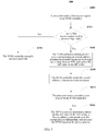
- FIG. 3 shows a method for accessing an NVM according to an embodiment of the present invention. As shown in FIG. 3 , the method 300 includes the following steps.
- S302 A processor sends a first access request to an NVM controller.
- the first access request carries first address information.
- the first address information is a physical address.
- the first address information may be a physical address of to-be-accessed memory data or a physical address of a page table entry.
- the processor When a cache miss occurs in the processor, when needing to access the memory data, and before sending an access request to the NVM controller, the processor needs to convert a virtual address into a physical address.
- the processor searches a TLB for a physical page number corresponding to a virtual page number.
- the virtual page number may be a partial field (such as a high-order field) of the virtual address of the memory data. If a TLB hit occurs, the processor obtains the physical page number of the memory data from the TLB, and determines the physical address of the to-be-accessed memory data based on the physical page number and by using a partial field (such as a low-order field) of the virtual address as an offset.
- the processor determines, based on the partial field of the virtual address of the memory data and a page table base address, a physical address of a page table entry that stores the physical page number, and sends an access request to the NVM controller.
- the access request carries the physical address of the page table entry.
- the processor may obtain, from the single-level page table by using an access request, a physical page number corresponding to a virtual page number of to-be-accessed memory data. More specifically, the processor may determine, based on a page table base address and by using a partial field (such as a high-order field or the virtual page number) of a virtual address of the memory data as an offset, a physical address of a page table entry that stores the physical page number, and reads, based on the physical address of the page table entry, the physical page number corresponding to the virtual page number recorded in the page table entry.
- a partial field such as a high-order field or the virtual page number
- the processor After reading the physical page number, the processor determines a physical address of the memory data by using the physical page number and a partial field (such as a low-order field) of the virtual address as an offset, and accesses the memory data based on the physical address of the memory data.
- a partial field such as a low-order field
- the page table base address may be stored in a dedicated register.
- the page table base address may be stored in a control register CR3, and the CR3 includes a page directory table physical memory base address. Therefore, the register is also referred to as a page-directory base address register (Page-Directory Base address Register, PDBR).
- PDBR Page-Directory Base address Register
- the physical page number corresponding to the virtual page number of the to-be-accessed memory data can be obtained only after the processor sends an access request to the processor for a plurality of times based on a level quantity of the page table.
- an entry of a first-level page table points to a second-level page table
- an entry of the second-level page table records the physical page number corresponding to the virtual page number of the memory data.
- the processor determines a physical address A based on a base address of the first-level page table stored in the register CR3 and by using a partial field of a virtual address (such as M high-order bits of the virtual address) of the memory data as an offset, and sends an access request based on the determined physical address A.
- Data read from the physical address A is a base address of the second-level page table.
- the processor determines a physical address B based on the base address of the second-level page table and by using a partial field of the virtual address (such as N middle-order bits of the virtual address) as an offset, and sends an access request based on the physical address B.
- Data read from the physical address B is a page table entry of the second-level page table.
- the page table entry records the physical page number corresponding to the virtual page number of the to-be-accessed memory data.
- the processor determines, based on the physical page number and by using a partial field of the virtual address (such as L low-order bits of the virtual address) as an offset, a physical address of the to-be-accessed memory data.
- step S304 After receiving the first access request, the NVM controller determines, based on the first address information, whether the first access request is used to access a page table; and if the first access request is not used to access the page table, step S306 is performed; or if the first access request is used to access the page table, step S308 is performed.
- the method 300 further includes: receiving, by the NVM controller, page table address information from the processor, where the NVM controller may determine, based on the page table address information, whether a received access request is used to access the page table.
- the page table address information may include an address stored in the register CR3 or an address of the register CR3.
- the register CR3 is configured to store a page table base address.
- the TLB miss inevitably triggers an exception of the processor.
- the processor may send an address of a register CR3 of a process that leads to the TLB miss or an address stored in the register CR3 to the NVM controller in an exception processing program.
- the NVM controller tracks access to the page table based on the base address stored in the CR3.
- the processor may alternatively send an address of a register CR3 corresponding to the thread or an address stored in the register CR3 to the NVM controller.
- the page table address information may further include information such as a level quantity of the page table, a parsing manner of each level of the page table, and a size of each page.
- the NVM controller may determine, based on the page table address information, whether the access request is access to the page table. For the multi-level page table, access to each level of the page table may be tracked based on the page table address information until the physical page number of the to-be-accessed memory data is obtained.
- the NVM controller can store only a limited amount of page table address information.
- replacement may be performed based on an algorithm. For example, a part of the page table address information may be reserved based on a replacement policy such as least recently used (Least Recently Used, LRU) or least frequently used (Least Frequently Used, LFU).
- LRU least recently used
- LFU least frequently used
- the NVM controller determines, based on the first address information and the page table address information, whether the first access request is used to access the page table. Specifically, the NVM controller may determine, by determining whether the first address information falls within a range of the page table address information, whether the first access request is used to access the page table. If the first address information falls within the range of the page table address information, it indicates that the first access request is used to access the page table. If the first address information does not fall within the range of the page table address information, it indicates that the first access request is used to access normal memory data instead of the page table.
- the NVM controller determines a page table size based on a quantity of page table entries and a size of each page table entry.
- An address range of the page table is: [page table base address, page table base address + page table size).
- the NVM controller determines, by determining whether the first address information falls within the address range of the page table, whether the first access request is used to access the page table. If the first address information falls within the address range of the page table, the first access request is used to access the page table.
- a base address of a first-level page table is stored in a control register
- a base address of a second-level page table is stored in a page table entry of the first-level page table, and so on, until a base address of a last-level page table is obtained and the physical page number of the to-be-accessed memory data is obtained from the last-level page table.
- the NVM controller may alternatively determine, based on a partial field (such as a high-order field) of the first address information and the page table base address, whether the first access request is used to access the page table. If the partial field of the first address information is the same as the page table base address maintained by the NVM controller, it indicates that the first address information falls within the range of the page table address information and that the first access request is used to access the page table.
- a partial field such as a high-order field
- S306 The NVM controller performs a normal access operation on the NVM based on the first access request.
- the first address information is the physical address of the to-be-accessed memory data, and the NVM controller normally accesses the NVM based on the first access request.
- the NVM controller searches, based on the first address information, an AIT cache for an NVM device address corresponding to the first address information. More specifically, the NVM controller searches the AIT cache for an NVM inner block number corresponding to a physical block number indicated by the first address information (such as a high-order field of the first address information), and accesses the NVM based on the NVM inner block number and the first address information (such as a low-order field of the first address information).
- the NVM controller obtains, based on second address information recorded in a page table entry indicated by the first address information, an AIT entry corresponding to the second address information from an AIT, and caches the AIT entry to an AIT cache.
- the first access request is used to access the page table entry, it indicates that the TLB miss occurs in the processor.
- the first access request is used to obtain a physical page number corresponding to a virtual page number of to-be-accessed data, and the first address information is a physical address of the page table entry that stores the physical page number.
- the NVM controller reads, based on the first address information, the second address information recorded by the page table entry.
- the second address information is specifically a physical page number. If the AIT entry corresponding to the second address information does not exist in the AIT cache, the NVM controller obtains the AIT entry corresponding to the second address information from the AIT, and caches the AIT entry to the AIT cache for subsequent use.
- the second address information may correspond to one or more AIT entries. More specifically, the AIT entry corresponding to the second address information is an AIT entry corresponding to one or more physical block numbers distributed in a physical page indicated by the second address information.
- S310 The NVM controller sends the second address information to the processor.
- the physical page indicated by the second address information is a physical page to be accessed by the processor. After obtaining the second address information, the NVM controller sends the second address information to the processor.
- the second address information may be the physical page number of the to-be-accessed memory data.
- the second address information may alternatively be a base address of a second-level page table.
- S312 The processor sends a second access request to the NVM controller, where the second access request carries the second address information.
- the processor receives the second address information (the physical page number), if the second address information is the physical page number of the to-be-accessed memory data, the processor further stores a correspondence between the virtual page number of the to-be-accessed memory data and the second address information in the TLB for subsequent use.
- the processor determines a physical address based on the second address information and by using a partial field of the virtual address of the to-be-accessed memory data as an offset, and adds the physical address to the second access request.
- the NVM controller determines, based on the second address information of the received second access request and the AIT entry that is pre-stored in the AIT cache, an NVM device address corresponding to the second address information, and accesses the NVM based on the NVM device address corresponding to the second address information.
- step S308 the NVM controller already stores, in the AIT cache, the AIT entry corresponding to the second address information. Therefore, after receiving the second access request, the NVM controller may directly find, in the AIT cache, the AIT entry corresponding to the second address information.
- the AIT entry records an NVM inner block number to be accessed by the second access request.
- the second access request carries the physical address determined by the processor by using the second address information as a base address and a partial field of the to-be-accessed memory data as an offset.
- the NVM controller determines an NVM inner block number corresponding to a physical block number in which a physical page indicated by the second address information is located, and determines an NVM inner address based on the NVM inner block number and by using a partial field of the physical address as an offset.
- the second access request may also be used to access the page table.
- the first access request is used to access a first-level page table
- the second access request is used to access a second-level page table.
- the method 300 may further include: determining, by the NVM controller based on the second address information, whether the second access request is used to access the page table; and if the second access request is used to access the page table, deleting, by the NVM controller, the AIT entry corresponding to the second address information from the AIT cache after obtaining, based on the second address information and the AIT entry that corresponds to the second address information and that is stored in the AIT cache, the NVM device address corresponding to the second address information.
- the deletion includes: using the AIT entry corresponding to the second address information as a replacement alternative to another AIT entry.
- the processor For access to the multi-level page table, after the physical page number corresponding to the virtual page number of the to-be-accessed memory data is obtained, the processor stores, in the TLB, a correspondence between the virtual page number and the physical page number. Subsequently, the processor can directly obtain, from the TLB, the physical page number corresponding to the to-be-accessed virtual page number. Therefore, for access to the page table, reusability of the AIT is not high. When the access ends, an AIT entry that is no longer used and that is related to the page table may be deleted, to reduce AIT cache pollution.
- the NVM controller may cache the AIT entry related to the page table by using some dedicated cache blocks, to reduce AIT cache pollution.
- the method 300 further includes: sending, by the processor after destructing a process, a page table invalidity message to the NVM controller, and invalidating, by the NVM controller after receiving the page table invalidity message from the processor, page table address information related to the process.
- the NVM controller monitors access of the processor to the page table.
- the NVM controller parses content of the page table to obtain a physical page number that may be subsequently accessed, prefetches an AIT entry corresponding to the physical page number from the AIT in advance before the processor really accesses the physical page number, and caches the prefetched AIT entry to the AIT cache. In this way, subsequent AIT cache misses are reduced, thereby increasing a data access speed of the NVM.
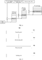
- FIG. 5 is a schematic diagram of a logical structure of an apparatus 500 for accessing a non-volatile memory according to an embodiment of the present invention.
- the apparatus 500 includes a receiving unit 502, a determining unit 504, a processing unit 506, and a sending unit 508.
- the receiving unit 502 is configured to receive a first access request from a processor, where the first access request carries first address information.
- the determining unit 504 is configured to determine, based on the first address information, whether the first access request is used to access a page table.
- the processing unit 506 is configured to: obtain, based on second address information recorded in a page table entry indicated by the first address information, an AIT entry corresponding to the second address information from an address indirection table AIT, and cache the AIT entry to an AIT cache, where the AIT is used to record a mapping relationship between address information and an NVM device address.
- the sending unit 508 is configured to send the second address information to the processor.
- the receiving unit 502 is further configured to receive a second access request from the processor, where the second access request carries the second address information.
- the processing unit 506 is further configured to: obtain, based on the second address information and the AIT entry in the AIT cache, an NVM device address corresponding to the second address information, and access the NVM based on the NVM device address corresponding to the second address information.
- the determining unit 504 is further configured to determine, based on the second address information, whether the second access request is used to access the page table. If the second access request is used to access the page table, the processing unit 506 is further configured to delete the AIT entry from the AIT cache after obtaining the NVM device address corresponding to the second address information.
- the receiving unit 502 is further configured to receive page table address information from the processor.
- the determining unit 504 is configured to determine, based on the first address information and the page table address information, whether the first access request is used to access the page table.
- the receiving unit 502 is further configured to receive page table invalidity information from the processor.
- the processing unit 506 is further configured to invalidate the page table address information based on the page table invalidity information.
- This embodiment of the present invention is an apparatus embodiment of the NVM controller. Feature descriptions of the embodiments of FIG. 1 to FIG. 4 are applicable to this embodiment of the present invention. Details are not described herein again.
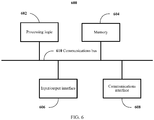
- FIG. 6 is a schematic diagram of a hardware structure of an apparatus 600 for accessing a non-volatile memory according to an embodiment of the present invention.
- the apparatus 600 includes a processing logic 602, a memory 604, an input/output interface 606, a communications interface 608, and a bus 610. Communication connection between the processing logic 602, the memory 604, the input/output interface 606, and the communications interface 608 is implemented by using the bus 610.
- the processing logic 602 is a control center of the apparatus 600, and configured to implement technical solutions provided in this embodiment of the present invention.
- the processing logic 602 may be a general purpose processor, a microprocessor, an application-specific integrated circuit, or one or more integrated circuits to implement the technical solutions provided in this embodiment of the present invention.
- the processing logic 602 is implemented by using the processor, the processing logic is configured to execute program code in the memory 604, to implement the technical solutions provided in this embodiment of the present invention.
- the memory 604 may be a read-only memory (Read Only Memory, ROM), a static storage device, a dynamic storage device, or a random access memory (Random Access Memory, RAM).
- ROM Read Only Memory
- RAM Random Access Memory
- the program code used to implement the technical solutions provided in this embodiment of the present invention is stored in the memory 604, and is executed by the processing logic 602.
- the memory 604 may be integrated with the processing logic 602 or integrated inside the processing logic 602, or may be one or more storage units independent of the processing logic 602.
- the program code executed by the processing logic 602 may be stored in an external storage device connected to the processing logic 602 or in the memory 604.
- the memory 604 is a RAM.
- the program code stored in the external storage device is copied into the memory 604 to be executed by the processing logic 602.
- a component for example, the processing logic 602 or the memory 604, configured to perform a particular function may be implemented by configuring a general component to perform a corresponding function or by using a dedicated component for specially performing the particular function. This is not limited in this application.
- the input/output interface 606 is configured to: receive input data and information, and output data such as an operation result.
- the communications interface 608 uses a transceiver apparatus, for example, but not limited to a transceiver, to implement communication between the apparatus 600 and another device or a communications network.
- a transceiver apparatus for example, but not limited to a transceiver, to implement communication between the apparatus 600 and another device or a communications network.
- the bus 610 may include a path that transmits information between parts (such as the processing logic 602, the memory 604, the input/output interface 606, and the communications interface 608) of the apparatus 600.
- the apparatus 600 shown in FIG. 6 shows merely the processing logic 602, the memory 604, the input/output interface 606, the communications interface 608, and the bus 610, in a specific implementation process, persons skilled in the art should understand that the apparatus 600 further includes other devices necessary for implementing normal running. In addition, based on a specific requirement, persons skilled in the art should understand that the apparatus 600 may further include a hardware device for implementing another additional function. Moreover, persons skilled in the art should understand that the apparatus 600 may alternatively include only devices necessary for implementing this embodiment of the present invention and not necessarily include all devices shown in FIG. 6 .
- the receiving unit 302 and the sending unit 308 shown in FIG. 3 may be implemented by the processing logic 602 shown in FIG. 6 in combination with the communications interface 608, and more specifically, may be implemented by executing the program code in the memory 604 by the processing logic 602 in combination with the communications interface 608.
- the determining unit 504 and the processing unit 506 shown in FIG. 5 may be implemented by the processing logic 602 shown in FIG. 6 , and more specifically, may be implemented by executing the program code in the memory 604 by the processing logic 602.
- the hardware structure shown in FIG. 6 and the foregoing descriptions are applicable to various apparatuses for accessing a non-volatile memory according to the embodiments of the present invention, and are applicable to various methods for accessing a non-volatile memory according to the embodiments of the present invention.
- the disclosed system, device, and method may be implemented in other manners.
- the apparatus embodiment described above is merely an example.
- the module division is merely logical function division and may be other division during implementation.
- a plurality of modules or components may be combined or integrated into another system, or some features may be ignored or not performed.
- the displayed or discussed mutual couplings or direct couplings or communication connections may be implemented by using some interfaces.
- the indirect couplings or communication connections between the apparatuses or modules may be implemented in an electronic form, a mechanical form, or another form.
- modules described as separate parts may or may not be physically separate, and parts displayed as modules may or may not be physical modules, that is, may be located in one position, or may be distributed on a plurality of network modules. Some or all of the modules may be selected according to actual needs to achieve the objectives of the solutions of the embodiments.
- function modules in the embodiments of the present invention may be integrated into one processing module, or each of the modules may exist alone physically, or two or more modules may be integrated into one module.
- the integrated module may be implemented in a form of hardware, or may be implemented in a form of hardware in addition to a software function module.
- the integrated unit may be stored in a computer-readable storage medium.
- the software functional module is stored in a storage medium and includes several instructions for instructing a computer device (which may be a personal computer, a server, or a network device) to perform some of the steps of the methods described in the embodiments of the present invention.
- the foregoing storage medium includes: any medium that can store program code, such as a removable hard disk, a read-only memory, a random access memory, a magnetic disk, or an optical disc.
Landscapes
- Engineering & Computer Science (AREA)
- Theoretical Computer Science (AREA)
- Physics & Mathematics (AREA)
- General Engineering & Computer Science (AREA)
- General Physics & Mathematics (AREA)
- Memory System Of A Hierarchy Structure (AREA)
Applications Claiming Priority (1)
| Application Number | Priority Date | Filing Date | Title |
|---|---|---|---|
| PCT/CN2016/112699 WO2018119773A1 (zh) | 2016-12-28 | 2016-12-28 | 非易失内存访问方法、装置和系统 |
Publications (3)
| Publication Number | Publication Date |
|---|---|
| EP3553665A1 true EP3553665A1 (de) | 2019-10-16 |
| EP3553665A4 EP3553665A4 (de) | 2020-01-29 |
| EP3553665B1 EP3553665B1 (de) | 2024-05-15 |
Family
ID=62710808
Family Applications (1)
| Application Number | Title | Priority Date | Filing Date |
|---|---|---|---|
| EP16925965.2A Active EP3553665B1 (de) | 2016-12-28 | 2016-12-28 | Zugangsverfahren, -vorrichtung und -system für nichtflüchtigen speicher |
Country Status (4)
| Country | Link |
|---|---|
| US (1) | US10997078B2 (de) |
| EP (1) | EP3553665B1 (de) |
| CN (1) | CN109219804B (de) |
| WO (1) | WO2018119773A1 (de) |
Families Citing this family (9)
| Publication number | Priority date | Publication date | Assignee | Title |
|---|---|---|---|---|
| US11347644B2 (en) * | 2018-10-15 | 2022-05-31 | Texas Instruments Incorporated | Distributed error detection and correction with hamming code handoff |
| CN113703660B (zh) * | 2020-05-22 | 2024-03-19 | 超聚变数字技术有限公司 | 数据预取方法和数据预取装置 |
| KR20220032808A (ko) | 2020-09-08 | 2022-03-15 | 삼성전자주식회사 | 프로세싱-인-메모리, 메모리 액세스 방법 및 메모리 액세스 장치 |
| KR20220049396A (ko) | 2020-10-14 | 2022-04-21 | 삼성전자주식회사 | 간접 어드레싱을 위한 시스템, 장치 및 방법 |
| CN114356793B (zh) * | 2021-11-25 | 2024-02-27 | 苏州浪潮智能科技有限公司 | 数据处理方法、装置、电子设备及存储介质 |
| CN114610655B (zh) * | 2022-05-10 | 2022-08-05 | 沐曦集成电路(上海)有限公司 | 连续数据访问处理装置和芯片 |
| CN114996024A (zh) * | 2022-07-29 | 2022-09-02 | 阿里巴巴(中国)有限公司 | 内存带宽监测方法、服务器和计算机可读存储介质 |
| US20260072843A1 (en) * | 2024-09-10 | 2026-03-12 | Apple Inc. | Adaptive Adjustment of Prefetch Constraints for Certain Workloads |
| CN120631801B (zh) * | 2025-08-12 | 2025-10-28 | 知合计算技术(杭州)有限公司 | 数据预取方法、装置及处理器 |
Family Cites Families (17)
| Publication number | Priority date | Publication date | Assignee | Title |
|---|---|---|---|---|
| CA1283222C (en) * | 1989-09-22 | 1991-04-16 | Howard Gene Sachs | Microprocessor having separate instruction and data interfaces |
| KR101466585B1 (ko) * | 2008-07-10 | 2014-11-28 | 삼성전자주식회사 | 메모리 장치 및 메모리 장치의 관리 방법 |
| JP5605238B2 (ja) * | 2011-01-25 | 2014-10-15 | ソニー株式会社 | メモリシステムおよびその動作方法 |
| CN103946819B (zh) * | 2011-09-30 | 2017-05-17 | 英特尔公司 | 用于非易失性系统存储器的统计耗损均衡 |
| WO2013095381A1 (en) * | 2011-12-20 | 2013-06-27 | Intel Corporation | Method and system for data de-duplication |
| BR112014015051B1 (pt) * | 2011-12-21 | 2021-05-25 | Intel Corporation | método e sistema para utilizar dicas de liberação de memória dentro de um sistema de computador |
| US9262336B2 (en) | 2011-12-23 | 2016-02-16 | Intel Corporation | Page miss handler including wear leveling logic |
| US10380030B2 (en) * | 2012-12-05 | 2019-08-13 | Arm Limited | Caching of virtual to physical address translations |
| CN103164343B (zh) * | 2013-02-27 | 2015-12-09 | 山东大学 | 基于相变存储器的分页、ecc校验及多位预取方法及其结构 |
| KR102432754B1 (ko) * | 2013-10-21 | 2022-08-16 | 에프엘씨 글로벌 리미티드 | 최종 레벨 캐시 시스템 및 이에 대응하는 방법 |
| CN103810112B (zh) * | 2014-01-28 | 2016-08-17 | 华中科技大学 | 一种非易失性内存系统及其管理方法 |
| KR20150139718A (ko) * | 2014-06-03 | 2015-12-14 | 에스케이하이닉스 주식회사 | 불휘발성 메모리를 제어하는 컨트롤러 및 그것을 포함하는 반도체 장치 |
| CN105354152B (zh) * | 2014-08-19 | 2018-06-26 | 华为技术有限公司 | 非易失性存储器及磨损均衡方法 |
| EP3217294B1 (de) * | 2014-11-28 | 2018-11-28 | Huawei Technologies Co. Ltd. | Dateizugangsverfahren und vorrichtung sowie speichervorrichtung |
| CN105786722B (zh) * | 2014-12-25 | 2020-10-27 | 研祥智能科技股份有限公司 | 基于异构混合内存的nvm内存擦写控制方法和系统 |
| CN105786721A (zh) * | 2014-12-25 | 2016-07-20 | 研祥智能科技股份有限公司 | 一种内存地址映射管理方法及处理器 |
| CN105786717B (zh) * | 2016-03-22 | 2018-11-16 | 华中科技大学 | 软硬件协同管理的dram-nvm层次化异构内存访问方法及系统 |
-
2016
- 2016-12-28 CN CN201680084386.6A patent/CN109219804B/zh active Active
- 2016-12-28 WO PCT/CN2016/112699 patent/WO2018119773A1/zh not_active Ceased
- 2016-12-28 EP EP16925965.2A patent/EP3553665B1/de active Active
-
2019
- 2019-06-27 US US16/455,466 patent/US10997078B2/en active Active
Also Published As
| Publication number | Publication date |
|---|---|
| WO2018119773A1 (zh) | 2018-07-05 |
| US20190324914A1 (en) | 2019-10-24 |
| EP3553665B1 (de) | 2024-05-15 |
| CN109219804A (zh) | 2019-01-15 |
| EP3553665A4 (de) | 2020-01-29 |
| US10997078B2 (en) | 2021-05-04 |
| CN109219804B (zh) | 2023-12-29 |
Similar Documents
| Publication | Publication Date | Title |
|---|---|---|
| US10997078B2 (en) | Method, apparatus, and non-transitory readable medium for accessing non-volatile memory | |
| CN108804350B (zh) | 一种内存访问方法及计算机系统 | |
| CN104346294B (zh) | 基于多级缓存的数据读/写方法、装置和计算机系统 | |
| CN110998549B (zh) | 地址转换缓存 | |
| US11341059B2 (en) | Using multiple memory elements in an input-output memory management unit for performing virtual address to physical address translations | |
| CN107111455B (zh) | 电子处理器架构以及缓存数据的方法 | |
| JP5628404B2 (ja) | キャッシュされたメモリデータを伴うキャッシュメモリ属性インジケータ | |
| CN111858404B (zh) | 地址转换的方法和系统、以及计算机可读介质 | |
| CN112631961B (zh) | 一种内存管理单元、地址转译方法以及处理器 | |
| US10019377B2 (en) | Managing cache coherence using information in a page table | |
| KR102281928B1 (ko) | 가변 변환 색인 버퍼(tlb) 인덱싱 | |
| CN111949572A (zh) | 页表条目合并方法、装置及电子设备 | |
| CN107870867B (zh) | 32位cpu访问大于4gb内存空间的方法与装置 | |
| CN111061655B (zh) | 存储设备的地址转换方法与设备 | |
| CN120523750A (zh) | 分层缓存系统中的预取管理 | |
| US8543792B1 (en) | Memory access techniques including coalesing page table entries | |
| CN117331853A (zh) | 缓存处理方法、装置、电子设备及介质 | |
| CN119621608A (zh) | 硬件辅助页表管理系统、方法、介质、程序产品及终端 | |
| CN114840452B (zh) | 一种控制部件 | |
| WO2023217255A1 (zh) | 数据处理方法、装置、处理器及计算机系统 | |
| CN107870870B (zh) | 访问超过地址总线宽度的内存空间 | |
| CN111198827B (zh) | 页表预取方法及装置 | |
| US7769979B1 (en) | Caching of page access parameters | |
| US11397691B2 (en) | Latency hiding for caches | |
| CN120541007A (zh) | 内存管理单元、处理器及缓存页表的方法 |
Legal Events
| Date | Code | Title | Description |
|---|---|---|---|
| STAA | Information on the status of an ep patent application or granted ep patent |
Free format text: STATUS: THE INTERNATIONAL PUBLICATION HAS BEEN MADE |
|
| PUAI | Public reference made under article 153(3) epc to a published international application that has entered the european phase |
Free format text: ORIGINAL CODE: 0009012 |
|
| STAA | Information on the status of an ep patent application or granted ep patent |
Free format text: STATUS: REQUEST FOR EXAMINATION WAS MADE |
|
| 17P | Request for examination filed |
Effective date: 20190709 |
|
| AK | Designated contracting states |
Kind code of ref document: A1 Designated state(s): AL AT BE BG CH CY CZ DE DK EE ES FI FR GB GR HR HU IE IS IT LI LT LU LV MC MK MT NL NO PL PT RO RS SE SI SK SM TR |
|
| AX | Request for extension of the european patent |
Extension state: BA ME |
|
| A4 | Supplementary search report drawn up and despatched |
Effective date: 20200108 |
|
| RIC1 | Information provided on ipc code assigned before grant |
Ipc: G06F 12/1027 20160101ALI20191220BHEP Ipc: G06F 12/08 20160101AFI20191220BHEP Ipc: G06F 12/02 20060101ALI20191220BHEP Ipc: G06F 12/1009 20160101ALI20191220BHEP |
|
| DAV | Request for validation of the european patent (deleted) | ||
| DAX | Request for extension of the european patent (deleted) | ||
| STAA | Information on the status of an ep patent application or granted ep patent |
Free format text: STATUS: EXAMINATION IS IN PROGRESS |
|
| 17Q | First examination report despatched |
Effective date: 20220128 |
|
| GRAP | Despatch of communication of intention to grant a patent |
Free format text: ORIGINAL CODE: EPIDOSNIGR1 |
|
| STAA | Information on the status of an ep patent application or granted ep patent |
Free format text: STATUS: GRANT OF PATENT IS INTENDED |
|
| INTG | Intention to grant announced |
Effective date: 20240117 |
|
| GRAS | Grant fee paid |
Free format text: ORIGINAL CODE: EPIDOSNIGR3 |
|
| GRAA | (expected) grant |
Free format text: ORIGINAL CODE: 0009210 |
|
| STAA | Information on the status of an ep patent application or granted ep patent |
Free format text: STATUS: THE PATENT HAS BEEN GRANTED |
|
| AK | Designated contracting states |
Kind code of ref document: B1 Designated state(s): AL AT BE BG CH CY CZ DE DK EE ES FI FR GB GR HR HU IE IS IT LI LT LU LV MC MK MT NL NO PL PT RO RS SE SI SK SM TR |
|
| REG | Reference to a national code |
Ref country code: CH Ref legal event code: EP Ref country code: GB Ref legal event code: FG4D |
|
| REG | Reference to a national code |
Ref country code: IE Ref legal event code: FG4D |
|
| REG | Reference to a national code |
Ref country code: DE Ref legal event code: R096 Ref document number: 602016087585 Country of ref document: DE |
|
| REG | Reference to a national code |
Ref country code: NL Ref legal event code: FP |
|
| REG | Reference to a national code |
Ref country code: LT Ref legal event code: MG9D |
|
| PG25 | Lapsed in a contracting state [announced via postgrant information from national office to epo] |
Ref country code: IS Free format text: LAPSE BECAUSE OF FAILURE TO SUBMIT A TRANSLATION OF THE DESCRIPTION OR TO PAY THE FEE WITHIN THE PRESCRIBED TIME-LIMIT Effective date: 20240915 |
|
| PG25 | Lapsed in a contracting state [announced via postgrant information from national office to epo] |
Ref country code: BG Free format text: LAPSE BECAUSE OF FAILURE TO SUBMIT A TRANSLATION OF THE DESCRIPTION OR TO PAY THE FEE WITHIN THE PRESCRIBED TIME-LIMIT Effective date: 20240515 |
|
| PG25 | Lapsed in a contracting state [announced via postgrant information from national office to epo] |
Ref country code: HR Free format text: LAPSE BECAUSE OF FAILURE TO SUBMIT A TRANSLATION OF THE DESCRIPTION OR TO PAY THE FEE WITHIN THE PRESCRIBED TIME-LIMIT Effective date: 20240515 Ref country code: FI Free format text: LAPSE BECAUSE OF FAILURE TO SUBMIT A TRANSLATION OF THE DESCRIPTION OR TO PAY THE FEE WITHIN THE PRESCRIBED TIME-LIMIT Effective date: 20240515 |
|
| PG25 | Lapsed in a contracting state [announced via postgrant information from national office to epo] |
Ref country code: GR Free format text: LAPSE BECAUSE OF FAILURE TO SUBMIT A TRANSLATION OF THE DESCRIPTION OR TO PAY THE FEE WITHIN THE PRESCRIBED TIME-LIMIT Effective date: 20240816 |
|
| PG25 | Lapsed in a contracting state [announced via postgrant information from national office to epo] |
Ref country code: PT Free format text: LAPSE BECAUSE OF FAILURE TO SUBMIT A TRANSLATION OF THE DESCRIPTION OR TO PAY THE FEE WITHIN THE PRESCRIBED TIME-LIMIT Effective date: 20240916 |
|
| REG | Reference to a national code |
Ref country code: AT Ref legal event code: MK05 Ref document number: 1687468 Country of ref document: AT Kind code of ref document: T Effective date: 20240515 |
|
| PG25 | Lapsed in a contracting state [announced via postgrant information from national office to epo] |
Ref country code: ES Free format text: LAPSE BECAUSE OF FAILURE TO SUBMIT A TRANSLATION OF THE DESCRIPTION OR TO PAY THE FEE WITHIN THE PRESCRIBED TIME-LIMIT Effective date: 20240515 |
|
| PG25 | Lapsed in a contracting state [announced via postgrant information from national office to epo] |
Ref country code: AT Free format text: LAPSE BECAUSE OF FAILURE TO SUBMIT A TRANSLATION OF THE DESCRIPTION OR TO PAY THE FEE WITHIN THE PRESCRIBED TIME-LIMIT Effective date: 20240515 |
|
| PG25 | Lapsed in a contracting state [announced via postgrant information from national office to epo] |
Ref country code: PL Free format text: LAPSE BECAUSE OF FAILURE TO SUBMIT A TRANSLATION OF THE DESCRIPTION OR TO PAY THE FEE WITHIN THE PRESCRIBED TIME-LIMIT Effective date: 20240515 |
|
| PG25 | Lapsed in a contracting state [announced via postgrant information from national office to epo] |
Ref country code: LV Free format text: LAPSE BECAUSE OF FAILURE TO SUBMIT A TRANSLATION OF THE DESCRIPTION OR TO PAY THE FEE WITHIN THE PRESCRIBED TIME-LIMIT Effective date: 20240515 |
|
| PG25 | Lapsed in a contracting state [announced via postgrant information from national office to epo] |
Ref country code: PT Free format text: LAPSE BECAUSE OF FAILURE TO SUBMIT A TRANSLATION OF THE DESCRIPTION OR TO PAY THE FEE WITHIN THE PRESCRIBED TIME-LIMIT Effective date: 20240916 Ref country code: PL Free format text: LAPSE BECAUSE OF FAILURE TO SUBMIT A TRANSLATION OF THE DESCRIPTION OR TO PAY THE FEE WITHIN THE PRESCRIBED TIME-LIMIT Effective date: 20240515 Ref country code: NO Free format text: LAPSE BECAUSE OF FAILURE TO SUBMIT A TRANSLATION OF THE DESCRIPTION OR TO PAY THE FEE WITHIN THE PRESCRIBED TIME-LIMIT Effective date: 20240815 Ref country code: LV Free format text: LAPSE BECAUSE OF FAILURE TO SUBMIT A TRANSLATION OF THE DESCRIPTION OR TO PAY THE FEE WITHIN THE PRESCRIBED TIME-LIMIT Effective date: 20240515 Ref country code: IS Free format text: LAPSE BECAUSE OF FAILURE TO SUBMIT A TRANSLATION OF THE DESCRIPTION OR TO PAY THE FEE WITHIN THE PRESCRIBED TIME-LIMIT Effective date: 20240915 Ref country code: HR Free format text: LAPSE BECAUSE OF FAILURE TO SUBMIT A TRANSLATION OF THE DESCRIPTION OR TO PAY THE FEE WITHIN THE PRESCRIBED TIME-LIMIT Effective date: 20240515 Ref country code: GR Free format text: LAPSE BECAUSE OF FAILURE TO SUBMIT A TRANSLATION OF THE DESCRIPTION OR TO PAY THE FEE WITHIN THE PRESCRIBED TIME-LIMIT Effective date: 20240816 Ref country code: FI Free format text: LAPSE BECAUSE OF FAILURE TO SUBMIT A TRANSLATION OF THE DESCRIPTION OR TO PAY THE FEE WITHIN THE PRESCRIBED TIME-LIMIT Effective date: 20240515 Ref country code: ES Free format text: LAPSE BECAUSE OF FAILURE TO SUBMIT A TRANSLATION OF THE DESCRIPTION OR TO PAY THE FEE WITHIN THE PRESCRIBED TIME-LIMIT Effective date: 20240515 Ref country code: BG Free format text: LAPSE BECAUSE OF FAILURE TO SUBMIT A TRANSLATION OF THE DESCRIPTION OR TO PAY THE FEE WITHIN THE PRESCRIBED TIME-LIMIT Effective date: 20240515 Ref country code: AT Free format text: LAPSE BECAUSE OF FAILURE TO SUBMIT A TRANSLATION OF THE DESCRIPTION OR TO PAY THE FEE WITHIN THE PRESCRIBED TIME-LIMIT Effective date: 20240515 Ref country code: RS Free format text: LAPSE BECAUSE OF FAILURE TO SUBMIT A TRANSLATION OF THE DESCRIPTION OR TO PAY THE FEE WITHIN THE PRESCRIBED TIME-LIMIT Effective date: 20240815 |
|
| PG25 | Lapsed in a contracting state [announced via postgrant information from national office to epo] |
Ref country code: DK Free format text: LAPSE BECAUSE OF FAILURE TO SUBMIT A TRANSLATION OF THE DESCRIPTION OR TO PAY THE FEE WITHIN THE PRESCRIBED TIME-LIMIT Effective date: 20240515 |
|
| PG25 | Lapsed in a contracting state [announced via postgrant information from national office to epo] |
Ref country code: EE Free format text: LAPSE BECAUSE OF FAILURE TO SUBMIT A TRANSLATION OF THE DESCRIPTION OR TO PAY THE FEE WITHIN THE PRESCRIBED TIME-LIMIT Effective date: 20240515 |
|
| PG25 | Lapsed in a contracting state [announced via postgrant information from national office to epo] |
Ref country code: CZ Free format text: LAPSE BECAUSE OF FAILURE TO SUBMIT A TRANSLATION OF THE DESCRIPTION OR TO PAY THE FEE WITHIN THE PRESCRIBED TIME-LIMIT Effective date: 20240515 |
|
| PG25 | Lapsed in a contracting state [announced via postgrant information from national office to epo] |
Ref country code: SK Free format text: LAPSE BECAUSE OF FAILURE TO SUBMIT A TRANSLATION OF THE DESCRIPTION OR TO PAY THE FEE WITHIN THE PRESCRIBED TIME-LIMIT Effective date: 20240515 Ref country code: RO Free format text: LAPSE BECAUSE OF FAILURE TO SUBMIT A TRANSLATION OF THE DESCRIPTION OR TO PAY THE FEE WITHIN THE PRESCRIBED TIME-LIMIT Effective date: 20240515 |
|
| PG25 | Lapsed in a contracting state [announced via postgrant information from national office to epo] |
Ref country code: SM Free format text: LAPSE BECAUSE OF FAILURE TO SUBMIT A TRANSLATION OF THE DESCRIPTION OR TO PAY THE FEE WITHIN THE PRESCRIBED TIME-LIMIT Effective date: 20240515 |
|
| PG25 | Lapsed in a contracting state [announced via postgrant information from national office to epo] |
Ref country code: SM Free format text: LAPSE BECAUSE OF FAILURE TO SUBMIT A TRANSLATION OF THE DESCRIPTION OR TO PAY THE FEE WITHIN THE PRESCRIBED TIME-LIMIT Effective date: 20240515 Ref country code: SK Free format text: LAPSE BECAUSE OF FAILURE TO SUBMIT A TRANSLATION OF THE DESCRIPTION OR TO PAY THE FEE WITHIN THE PRESCRIBED TIME-LIMIT Effective date: 20240515 Ref country code: RO Free format text: LAPSE BECAUSE OF FAILURE TO SUBMIT A TRANSLATION OF THE DESCRIPTION OR TO PAY THE FEE WITHIN THE PRESCRIBED TIME-LIMIT Effective date: 20240515 Ref country code: EE Free format text: LAPSE BECAUSE OF FAILURE TO SUBMIT A TRANSLATION OF THE DESCRIPTION OR TO PAY THE FEE WITHIN THE PRESCRIBED TIME-LIMIT Effective date: 20240515 Ref country code: DK Free format text: LAPSE BECAUSE OF FAILURE TO SUBMIT A TRANSLATION OF THE DESCRIPTION OR TO PAY THE FEE WITHIN THE PRESCRIBED TIME-LIMIT Effective date: 20240515 Ref country code: CZ Free format text: LAPSE BECAUSE OF FAILURE TO SUBMIT A TRANSLATION OF THE DESCRIPTION OR TO PAY THE FEE WITHIN THE PRESCRIBED TIME-LIMIT Effective date: 20240515 |
|
| PG25 | Lapsed in a contracting state [announced via postgrant information from national office to epo] |
Ref country code: IT Free format text: LAPSE BECAUSE OF FAILURE TO SUBMIT A TRANSLATION OF THE DESCRIPTION OR TO PAY THE FEE WITHIN THE PRESCRIBED TIME-LIMIT Effective date: 20240515 |
|
| REG | Reference to a national code |
Ref country code: DE Ref legal event code: R097 Ref document number: 602016087585 Country of ref document: DE |
|
| PLBE | No opposition filed within time limit |
Free format text: ORIGINAL CODE: 0009261 |
|
| STAA | Information on the status of an ep patent application or granted ep patent |
Free format text: STATUS: NO OPPOSITION FILED WITHIN TIME LIMIT |
|
| 26N | No opposition filed |
Effective date: 20250218 |
|
| PG25 | Lapsed in a contracting state [announced via postgrant information from national office to epo] |
Ref country code: SI Free format text: LAPSE BECAUSE OF FAILURE TO SUBMIT A TRANSLATION OF THE DESCRIPTION OR TO PAY THE FEE WITHIN THE PRESCRIBED TIME-LIMIT Effective date: 20240515 |
|
| PG25 | Lapsed in a contracting state [announced via postgrant information from national office to epo] |
Ref country code: MC Free format text: LAPSE BECAUSE OF FAILURE TO SUBMIT A TRANSLATION OF THE DESCRIPTION OR TO PAY THE FEE WITHIN THE PRESCRIBED TIME-LIMIT Effective date: 20240515 |
|
| REG | Reference to a national code |
Ref country code: CH Ref legal event code: PL |
|
| PG25 | Lapsed in a contracting state [announced via postgrant information from national office to epo] |
Ref country code: LU Free format text: LAPSE BECAUSE OF NON-PAYMENT OF DUE FEES Effective date: 20241228 |
|
| PG25 | Lapsed in a contracting state [announced via postgrant information from national office to epo] |
Ref country code: SE Free format text: LAPSE BECAUSE OF FAILURE TO SUBMIT A TRANSLATION OF THE DESCRIPTION OR TO PAY THE FEE WITHIN THE PRESCRIBED TIME-LIMIT Effective date: 20240515 |
|
| REG | Reference to a national code |
Ref country code: BE Ref legal event code: MM Effective date: 20241231 |
|
| PG25 | Lapsed in a contracting state [announced via postgrant information from national office to epo] |
Ref country code: BE Free format text: LAPSE BECAUSE OF NON-PAYMENT OF DUE FEES Effective date: 20241231 |
|
| PG25 | Lapsed in a contracting state [announced via postgrant information from national office to epo] |
Ref country code: FR Free format text: LAPSE BECAUSE OF NON-PAYMENT OF DUE FEES Effective date: 20241231 |
|
| PG25 | Lapsed in a contracting state [announced via postgrant information from national office to epo] |
Ref country code: CH Free format text: LAPSE BECAUSE OF NON-PAYMENT OF DUE FEES Effective date: 20241231 |
|
| PG25 | Lapsed in a contracting state [announced via postgrant information from national office to epo] |
Ref country code: IE Free format text: LAPSE BECAUSE OF NON-PAYMENT OF DUE FEES Effective date: 20241228 |
|
| PGFP | Annual fee paid to national office [announced via postgrant information from national office to epo] |
Ref country code: NL Payment date: 20251112 Year of fee payment: 10 |
|
| PGFP | Annual fee paid to national office [announced via postgrant information from national office to epo] |
Ref country code: DE Payment date: 20251104 Year of fee payment: 10 |
|
| PGFP | Annual fee paid to national office [announced via postgrant information from national office to epo] |
Ref country code: GB Payment date: 20251114 Year of fee payment: 10 |