EP3553624B1 - Serrage efficace dans des alimentations électriques - Google Patents
Serrage efficace dans des alimentations électriques Download PDFInfo
- Publication number
- EP3553624B1 EP3553624B1 EP19167221.1A EP19167221A EP3553624B1 EP 3553624 B1 EP3553624 B1 EP 3553624B1 EP 19167221 A EP19167221 A EP 19167221A EP 3553624 B1 EP3553624 B1 EP 3553624B1
- Authority
- EP
- European Patent Office
- Prior art keywords
- voltage
- transistor
- switch
- power supply
- coupled
- Prior art date
- Legal status (The legal status is an assumption and is not a legal conclusion. Google has not performed a legal analysis and makes no representation as to the accuracy of the status listed.)
- Active
Links
Images

Classifications
-
- G—PHYSICS
- G05—CONTROLLING; REGULATING
- G05F—SYSTEMS FOR REGULATING ELECTRIC OR MAGNETIC VARIABLES
- G05F1/00—Automatic systems in which deviations of an electric quantity from one or more predetermined values are detected at the output of the system and fed back to a device within the system to restore the detected quantity to its predetermined value or values, i.e. retroactive systems
- G05F1/10—Regulating voltage or current
- G05F1/46—Regulating voltage or current wherein the variable actually regulated by the final control device is DC
- G05F1/56—Regulating voltage or current wherein the variable actually regulated by the final control device is DC using semiconductor devices in series with the load as final control devices
- G05F1/562—Regulating voltage or current wherein the variable actually regulated by the final control device is DC using semiconductor devices in series with the load as final control devices with a threshold detection shunting the control path of the final control device
-
- G—PHYSICS
- G05—CONTROLLING; REGULATING
- G05F—SYSTEMS FOR REGULATING ELECTRIC OR MAGNETIC VARIABLES
- G05F1/00—Automatic systems in which deviations of an electric quantity from one or more predetermined values are detected at the output of the system and fed back to a device within the system to restore the detected quantity to its predetermined value or values, i.e. retroactive systems
- G05F1/10—Regulating voltage or current
- G05F1/46—Regulating voltage or current wherein the variable actually regulated by the final control device is DC
- G05F1/56—Regulating voltage or current wherein the variable actually regulated by the final control device is DC using semiconductor devices in series with the load as final control devices
- G05F1/565—Regulating voltage or current wherein the variable actually regulated by the final control device is DC using semiconductor devices in series with the load as final control devices sensing a condition of the system or its load in addition to means responsive to deviations in the output of the system, e.g. current, voltage, power factor
-
- G—PHYSICS
- G05—CONTROLLING; REGULATING
- G05F—SYSTEMS FOR REGULATING ELECTRIC OR MAGNETIC VARIABLES
- G05F1/00—Automatic systems in which deviations of an electric quantity from one or more predetermined values are detected at the output of the system and fed back to a device within the system to restore the detected quantity to its predetermined value or values, i.e. retroactive systems
- G05F1/10—Regulating voltage or current
- G05F1/46—Regulating voltage or current wherein the variable actually regulated by the final control device is DC
- G05F1/56—Regulating voltage or current wherein the variable actually regulated by the final control device is DC using semiconductor devices in series with the load as final control devices
- G05F1/575—Regulating voltage or current wherein the variable actually regulated by the final control device is DC using semiconductor devices in series with the load as final control devices characterised by the feedback circuit
-
- H—ELECTRICITY
- H02—GENERATION; CONVERSION OR DISTRIBUTION OF ELECTRIC POWER
- H02M—APPARATUS FOR CONVERSION BETWEEN AC AND AC, BETWEEN AC AND DC, OR BETWEEN DC AND DC, AND FOR USE WITH MAINS OR SIMILAR POWER SUPPLY SYSTEMS; CONVERSION OF DC OR AC INPUT POWER INTO SURGE OUTPUT POWER; CONTROL OR REGULATION THEREOF
- H02M3/00—Conversion of DC power input into DC power output
- H02M3/02—Conversion of DC power input into DC power output without intermediate conversion into AC
- H02M3/04—Conversion of DC power input into DC power output without intermediate conversion into AC by static converters
- H02M3/10—Conversion of DC power input into DC power output without intermediate conversion into AC by static converters using discharge tubes with control electrode or semiconductor devices with control electrode
- H02M3/145—Conversion of DC power input into DC power output without intermediate conversion into AC by static converters using discharge tubes with control electrode or semiconductor devices with control electrode using devices of a triode or transistor type requiring continuous application of a control signal
- H02M3/155—Conversion of DC power input into DC power output without intermediate conversion into AC by static converters using discharge tubes with control electrode or semiconductor devices with control electrode using devices of a triode or transistor type requiring continuous application of a control signal using semiconductor devices only
- H02M3/156—Conversion of DC power input into DC power output without intermediate conversion into AC by static converters using discharge tubes with control electrode or semiconductor devices with control electrode using devices of a triode or transistor type requiring continuous application of a control signal using semiconductor devices only with automatic control of output voltage or current, e.g. switching regulators
- H02M3/158—Conversion of DC power input into DC power output without intermediate conversion into AC by static converters using discharge tubes with control electrode or semiconductor devices with control electrode using devices of a triode or transistor type requiring continuous application of a control signal using semiconductor devices only with automatic control of output voltage or current, e.g. switching regulators including plural semiconductor devices as final control devices for a single load
-
- H—ELECTRICITY
- H03—ELECTRONIC CIRCUITRY
- H03K—PULSE TECHNIQUE
- H03K5/00—Manipulating of pulses not covered by one of the other main groups of this subclass
- H03K5/22—Circuits having more than one input and one output for comparing pulses or pulse trains with each other according to input signal characteristics, e.g. slope, integral
- H03K5/24—Circuits having more than one input and one output for comparing pulses or pulse trains with each other according to input signal characteristics, e.g. slope, integral the characteristic being amplitude
Definitions
- Power supplies are used virtually in every electronic device primarily for converting alternate current (AC) electrical input that may be vary in voltage due to power line conditions and load factors into a constant direct current (DC) output to power the internal circuitry of the electronic device.
- AC alternate current
- DC direct current
- a linear regulator is a system used to maintain a steady voltage. The resistance of the regulator varies in accordance with the load resulting in a constant output voltage.
- the regulating device is made to act like a variable resistor, continuously adjusting a voltage divider network to maintain a constant output voltage and continually dissipating the difference between the input and regulated voltages as waste heat.
- a switching regulator uses an active device that switches on and off to maintain an average value of output.
- a low-dropout or LDO regulator is a DC linear voltage regulator that can regulate the output voltage even when the supply voltage is very close to the output voltage.
- the voltage regulator is forced into the so-called pass-through mode (PTM) when the input supply voltage is too low for regulation, in which case the output pass device will be fully opened, clamping the output to the input.
- PTM pass-through mode
- Large silicon area is often required to fabricate the output pass device to minimize the resistance and reduce the voltage drop across it. Failing to fully open that device will lead to significant silicon area.
- WO 1995/024066 A1 describes a current limited low dropout voltage circuit for coupling between first and second power supply terminals and an output terminal for providing a current limited low dropout voltage having a MOS pass transistor (PI) coupled in series between the first power supply terminal and the output terminal, a drive circuit (P2-P5) coupled to the gate of the MOS pass transistor, circuitry for limiting the gate-source voltage of the MOS pass transistor to limit the maximum current therethrough to a first maximum current level when the voltage between the second power supply terminal and the output terminal is less than a predetermined value, and circuitry for limiting the gate-source voltage of the MOS pass transistor to limit the maximum current therethrough to a second maximum current level when the source to drain voltage of the MOS pass transistor is greater than a predetermined voltage difference and the voltage between the output terminal and the second power supply terminal is greater than the predetermined value, the second maximum current level being greater than the first maximum current level.
- PI MOS pass transistor
- P2-P5 drive circuit
- EP 3 051 378 A1 describes an LDO circuit that comprises a pass element, and input stage, a current sink, a comparator and a control circuit.
- the pass element is configured to generate an output voltage depending on a gate signal and on an input voltage.
- the input stage is configured to generate a steering signal based on a deviation between a first reference signal and a feedback signal, the feedback signal being based on the output voltage.
- the current sink is controlled by a steering signal and connected between the gate control terminal and a reference terminal.
- the comparator is configured to compare the steering signal to a second reference signal and to generate a switch signal based on the comparison.
- the control circuit comprises a first current path and is configured to suspend, in particular temporarily suspend, the first current path depending on the switch signal.
- US 2009/206807 A1 describes voltage regulator including an overcurrent protection circuit, which is capable of enhancing accuracy of a limit current value and a short-circuit current value, and suppressing electric power loss when an overcurrent flows through an output transistor.
- the overcurrent protection circuit includes: an output current detection transistor controlled by an output voltage of an error amplifier circuit, for feeding a detection current; a detection resistor for generating a detection voltage based on the detection current; a second error amplifier circuit for amplifying a difference between a voltage set by a second reference voltage and a divided voltage, and the voltage of the detection resistor, and outputting the amplified difference; and an output current limiting circuit in which a gate thereof is controlled by an output of the second error amplifier circuit, for controlling a gate voltage of the output transistor. Further, the second reference voltage is supplied from a temperature detection circuit.
- US 2017/102724 A1 describes a voltage regulator that includes an input terminal to receive an input voltage, an output terminal to supply an output voltage, a power transistor, a differential amplifier, a driver, a dropout detector and a bias current limiter.
- the differential amplifier provides a drive signal based on a difference between a voltage reference and a feedback signal corresponding to the output voltage.
- the driver includes an impedance device, and a driver transistor that receives the drive signal so as to vary a bias current to a control terminal of the power transistor.
- the dropout detector and the bias current limiter is coupled to the input terminal, the impedance device, and the output terminal and includes first and second transistors coupled together, and a bias current generator coupled to the second transistor.
- a power supply comprising: an input voltage port configured to receive an input supply voltage;
- the power supply further includes a biasing current source coupled to the drain of the first transistor and a drain of the third transistor.
- the third transistor is also coupled to ground.
- the voltage at the feedback port is configured to vary proportionately to the output voltage.
- the second comparator is configured to control the third transistor when the voltage at the feedback port is lower than the fixed reference voltage.
- a method for regulating input voltage in a power supply comprising: comparing the voltage at the feedback port with the fixed reference voltage and, if the voltage at the feedback port is lower than the fixed reference voltage, using the cutoff switch to cut off the power supply from the first switch.
- the method further includes using the third transistor to control the gate of the second transistor when the voltage at the feedback port is lower than the fixed reference voltage.
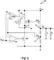
- Figure 1 illustrates a power supply 100 that includes a cutoff switch 102.
- the power supply 100 also includes a first comparator 104 to control the cutoff switch 102.
- a first switch M1 and a second switch M2 are included in a mirror configuration to regulate the output voltage V o .
- the second switch M2 is the main regulator switch that typically occupies the largest space on a semiconductor wafer on which the components of the power supply 100 are fabricated.
- the source of the first switch M1 is coupled to the cutoff switch 102 in series, that is, when the cutoff switch 102 is open, the source of the first switch M1 is disconnected from supply.
- the drain and the gate of the first switch M1 are coupled together.
- the source of the second switch M2 is coupled to the input power supply that is to be regulated.
- the drain of the second switch M2 is coupled to an output port 114.
- the output port 114 may be coupled to a capacitor C L and a resistor R L .
- a feedback port 112 is included.
- the feedback port 112 has a voltage V fb that is inputted to the first comparator 104 and a second comparator 106.
- the second comparator 106 is coupled to a third switch M3 and the second comparator 106 controls the gate of the third switch M3.
- a reference voltage V REF is inputted to the second input ports of the first comparator 104 and the second comparator 106.
- Biasing current I d is generated by a biasing current source 110 and inputted to the drain of the third switch M3.
- the biasing current Id is provided establish predetermined voltages or currents at various points in the power supply 100.
- the third switch M3 is provided to drive the main output device, e.g., the second switch M2 in the pass-through mode.
- the pass-through mode occurs when the input supply voltage falls below a selected threshold. In the pass-through mode, wherein the gate of M2 is pulled down by the front regulation stage, M1 needs to be disabled to prevent excessively large current draining into M3. Otherwise the gate voltage of M2 would remain at an elevated level, preventing the switch M2 from being fully opened, which in turn would necessitate a much larger area for silicon fabrication to handled elevated of passing through current.
- the power supply 100 is configured to provide a constant output voltage V o . But, when the input supply voltage V IN falls below a selected threshold, the output voltage V o also falls below another preselected threshold. If the input supply voltage VIN remains above the selected threshold, the output voltage V o remains constant even when the input supply voltage V IN fluctuates.
- Vo falls below the preselected threshold
- the feedback voltage V fb at the feedback port 112 falls below the reference voltage V REF .
- V fb falls below V REF
- the first comparator 104 turns off the cutoff switch 102, thus cutting of current to the first switch M1.
- the second comparator 106 applies gate voltage at the third switch M3. Cutting of current to the first switch M1 enables pulling the gate of the second switch M2 to close to ground.
- a high value resistor is placed in between the first switch M1 and the third switch M3 at the place shown by the arrow 108.
- the gate of the second switch M2 needs to be pulled down to maximize the output voltage.
- a high value resistor at the line 108 could limit the drain current to the third switch M3, the gate voltage of the second switch M2 is held up at a higher value than needed making a much larger size of the switch M2 necessary.
- the feedback port 112 may be the same as the output port that provides the voltage V o . In other examples, where a lower fixed V REF is used, the feedback port 112 may have a voltage lower than V o .
- FIG. 2 illustrates a method 200 for cutting off supply to a switch in the plurality of switches in a mirror configuration.
- step 202 voltage at a feedback port is compared, using a comparator, with a fixed reference voltage.
- step 204 a determination is made if the voltage at the feedback port is lower than the fixed reference voltage. If so, supply to a switch in the plurality of switched is cutoff using a cutoff switch that is coupled to the drain of the switch being cutoff from the power supply.
- a third switch that is coupled between the source of the switch being cutoff from power supply and ground, is turned on.
- a power supply is disclosed.
- the power supply includes a first switch and a second switch.
- the gate of the first switch is coupled to the gate of the second switch.
- the power supply further includes a cutoff switch coupled between the first switch and an input voltage port.
- a comparator is included for comparing a voltage at a feedback port with a fixed reference voltage. The comparator opens the cutoff switch when the voltage at the feedback port is lower than the fixed reference voltage.
Landscapes
- Engineering & Computer Science (AREA)
- Physics & Mathematics (AREA)
- Electromagnetism (AREA)
- General Physics & Mathematics (AREA)
- Radar, Positioning & Navigation (AREA)
- Automation & Control Theory (AREA)
- Nonlinear Science (AREA)
- Power Engineering (AREA)
- Electronic Switches (AREA)
- Dc-Dc Converters (AREA)
- Continuous-Control Power Sources That Use Transistors (AREA)
- Direct Current Feeding And Distribution (AREA)
Claims (7)
- Alimentation électrique (100), comprenant :un port de tension d'entrée configuré pour recevoir une tension d'alimentation d'entrée (Vin) ;un premier transistor (M1) et un deuxième transistor (M2) dans une configuration miroir dans laquelle une grille du premier transistor est couplée à une grille du deuxième transistor et un drain du premier transistor est connecté à la grille du premier transistor ;un interrupteur de coupure (l02) couplé entre le premier transistor et le port de tension d'entrée ;un port de sortie (114) configuré pour fournir une tension de sortie (V0), le deuxième transistor étant couplé entre le port de tension d'entrée et le port de sortie ;un troisième transistor (M3) couplé à un drain du premier transistor ; etun port de rétroaction ; l'alimentation électrique étant caractérisée en ce qu'elle comprend en outre :un comparateur (104) pour comparer une tension (Vfb) au port de rétroaction avec une tension de référence fixe, le comparateur étant configuré pour ouvrir l'interrupteur de coupure lorsque la tension au port de rétroaction (112) est inférieure à la tension de référence fixe ; etun second comparateur (106) couplé pour recevoir la tension de référence fixe et la tension au port de rétroaction afin de commander la grille du troisième transistor.
- Alimentation électrique selon la revendication 1, comprenant en outre une source de courant de polarisation (110) couplée au drain du premier transistor et à un drain du troisième transistor.
- Alimentation électrique selon la revendication 1 ou 2, dans laquelle le troisième transistor est également couplé à la masse.
- Alimentation électrique selon n'importe quelle revendication précédente, dans laquelle la tension au port de rétroaction est configurée pour varier proportionnellement à ladite tension de sortie.
- Alimentation électrique selon n'importe quelle revendication précédente, dans laquelle le second comparateur est configuré pour commander le troisième transistor lorsque la tension au port de rétroaction est inférieure à la tension de référence fixe.
- Procédé de régulation de tension d'entrée dans une alimentation électrique (100) selon n'importe quelle revendication précédente, le procédé étant caractérisé en ce qu'il comprend :
la comparaison de la tension au port de rétroaction (Vfb) avec la tension de référence fixe et, si la tension au port de rétroaction est inférieure à la tension de référence fixe, la coupure de l'alimentation à partir du premier transistor (M1) à l'aide de l'interrupteur de coupure (102). - Procédé selon la revendication 6, le procédé comprenant en outre l'utilisation (206) du troisième transistor (M3) pour commander la grille du deuxième transistor (M2) lorsque la tension au niveau du port de rétroaction est inférieure à la tension de référence fixe.
Applications Claiming Priority (1)
| Application Number | Priority Date | Filing Date | Title |
|---|---|---|---|
| US15/952,583 US10317921B1 (en) | 2018-04-13 | 2018-04-13 | Effective clamping in power supplies |
Publications (2)
| Publication Number | Publication Date |
|---|---|
| EP3553624A1 EP3553624A1 (fr) | 2019-10-16 |
| EP3553624B1 true EP3553624B1 (fr) | 2021-09-15 |
Family
ID=66092126
Family Applications (1)
| Application Number | Title | Priority Date | Filing Date |
|---|---|---|---|
| EP19167221.1A Active EP3553624B1 (fr) | 2018-04-13 | 2019-04-04 | Serrage efficace dans des alimentations électriques |
Country Status (3)
| Country | Link |
|---|---|
| US (1) | US10317921B1 (fr) |
| EP (1) | EP3553624B1 (fr) |
| CN (1) | CN110380610B (fr) |
Families Citing this family (2)
| Publication number | Priority date | Publication date | Assignee | Title |
|---|---|---|---|---|
| CN111474974B (zh) * | 2020-04-30 | 2022-07-01 | 上海维安半导体有限公司 | 一种提高ldo由重载突变到轻载或空载时瞬态响应的方法 |
| US11656643B2 (en) * | 2021-05-12 | 2023-05-23 | Nxp Usa, Inc. | Capless low dropout regulation |
Family Cites Families (24)
| Publication number | Priority date | Publication date | Assignee | Title |
|---|---|---|---|---|
| US5539603A (en) * | 1994-03-02 | 1996-07-23 | Maxim Integrated Products | Current protection method and apparatus and current protected low dropout voltage circuits |
| FR2798480B1 (fr) * | 1999-09-10 | 2001-10-26 | St Microelectronics Sa | Regulateur de tension |
| US6411068B1 (en) * | 2000-10-03 | 2002-06-25 | Bae Systems Information & Electronic Systems Integration, Inc. | Self-oscillating switching regulator |
| JP4587804B2 (ja) * | 2004-12-22 | 2010-11-24 | 株式会社リコー | ボルテージレギュレータ回路 |
| US7221213B2 (en) * | 2005-08-08 | 2007-05-22 | Aimtron Technology Corp. | Voltage regulator with prevention from overvoltage at load transients |
| US7728569B1 (en) * | 2007-04-10 | 2010-06-01 | Altera Corporation | Voltage regulator circuitry with adaptive compensation |
| JP5099505B2 (ja) * | 2008-02-15 | 2012-12-19 | セイコーインスツル株式会社 | ボルテージレギュレータ |
| CN101841240B (zh) * | 2010-04-12 | 2012-08-29 | 无锡中星微电子有限公司 | 电源转换器和误差放大器 |
| CN102237812B (zh) * | 2010-04-26 | 2013-06-12 | 辉芒微电子(深圳)有限公司 | 原边反馈开关电源控制器和开关电源系统 |
| US8456784B2 (en) * | 2010-05-03 | 2013-06-04 | Freescale Semiconductor, Inc. | Overvoltage protection circuit for an integrated circuit |
| US8531194B2 (en) * | 2011-03-24 | 2013-09-10 | Freescale Semiconductor, Inc. | Selectable threshold reset circuit |
| JP2013046496A (ja) * | 2011-08-24 | 2013-03-04 | Fujitsu Semiconductor Ltd | 制御回路、電源装置及び電源の制御方法 |
| US20130063116A1 (en) * | 2011-09-14 | 2013-03-14 | Fairchild Semiconductor Corporation | True reverse current blocking system |
| CN102420005B (zh) * | 2011-11-30 | 2014-02-19 | 中国科学院微电子研究所 | 一种电流模灵敏放大器及具有该灵敏放大器的存储器 |
| CN202794314U (zh) * | 2012-07-19 | 2013-03-13 | 快捷半导体(苏州)有限公司 | 一种功率开关管的过流检测电路 |
| US8975882B2 (en) * | 2012-10-31 | 2015-03-10 | Taiwan Semiconductor Manufacturing Co., Ltd. | Regulator with improved wake-up time |
| KR101974024B1 (ko) * | 2012-11-26 | 2019-05-02 | 온세미컨덕터코리아 주식회사 | 저전압 차단 회로, 이를 포함하는 스위치 제어 회로 및 전력 공급 장치 |
| EP2779452B1 (fr) * | 2013-03-13 | 2018-08-15 | Nxp B.V. | Circuit et procédé de source de courant commutable |
| US9748849B2 (en) * | 2013-07-08 | 2017-08-29 | Fairchild Korea Semiconductor Ltd. | Power supply |
| EP3051378B1 (fr) * | 2015-01-28 | 2021-05-12 | ams AG | Circuit régulateur à faible chute de tension et procédé pour commander une tension d'un tel circuit |
| US9645594B2 (en) * | 2015-10-13 | 2017-05-09 | STMicroelectronics Design & Application S.R.O. | Voltage regulator with dropout detector and bias current limiter and associated methods |
| CN105490537B (zh) * | 2015-12-29 | 2017-11-24 | 无锡中感微电子股份有限公司 | 一种电源管理电路 |
| US10444778B2 (en) * | 2016-08-09 | 2019-10-15 | Nxp Usa, Inc. | Voltage regulator |
| CN106505835B (zh) * | 2016-12-12 | 2019-08-27 | 北京集创北方科技股份有限公司 | 电压钳位电路以及dc-dc变换器 |
-
2018
- 2018-04-13 US US15/952,583 patent/US10317921B1/en active Active
-
2019
- 2019-04-04 EP EP19167221.1A patent/EP3553624B1/fr active Active
- 2019-04-11 CN CN201910291542.1A patent/CN110380610B/zh active Active
Also Published As
| Publication number | Publication date |
|---|---|
| US10317921B1 (en) | 2019-06-11 |
| EP3553624A1 (fr) | 2019-10-16 |
| CN110380610B (zh) | 2024-08-13 |
| CN110380610A (zh) | 2019-10-25 |
Similar Documents
| Publication | Publication Date | Title |
|---|---|---|
| US8169202B2 (en) | Low dropout regulators | |
| US12079018B2 (en) | Voltage regulator | |
| US8217638B1 (en) | Linear regulation for use with electronic circuits | |
| US7339775B2 (en) | Overcurrent protection circuit and DC power supply | |
| EP1729197A1 (fr) | Régulateur de tension à faible tension de déchêt avec compensation du pôle zéro. | |
| US8026708B2 (en) | Voltage regulator | |
| US7602162B2 (en) | Voltage regulator with over-current protection | |
| EP4220334A1 (fr) | Procédé et appareil permettant de limiter le courant d'appel pour le démarrage d'un régulateur à faible chute de tension | |
| EP2894537B1 (fr) | Régulateur de tension | |
| US7586364B2 (en) | Power supply voltage controlling circuit and semiconductor integrated circuit | |
| US10761549B2 (en) | Voltage sensing mechanism to minimize short-to-ground current for low drop-out and bypass mode regulators | |
| US9645593B2 (en) | Voltage regulator | |
| EP1669831A1 (fr) | Étape de sortie d'un régulateur de voltage avec transistors MOS à basse tension | |
| US20100090755A1 (en) | Current Limiting Load Switch with Dynamically Generated Tracking Reference Voltage | |
| US10571942B2 (en) | Overcurrent limiting circuit, overcurrent limiting method, and power supply circuit | |
| US9966941B2 (en) | Wide input range, low output voltage power supply | |
| US10310526B2 (en) | Quiescent current limitation for a low-dropout regulator in dropout condition | |
| KR20100094365A (ko) | 전압 레귤레이터 | |
| EP3588238B1 (fr) | Circuits de régulation de tension ayant des boucles de commande activées séparément | |
| US8373398B2 (en) | Area-efficient voltage regulators | |
| US9740222B2 (en) | Overcurrent protection circuit for controlling a gate of an output transistor based on an output current | |
| EP3553624B1 (fr) | Serrage efficace dans des alimentations électriques | |
| US8884596B2 (en) | Dynamic control of frequency compensation for improved over-voltage protection in a switching regulator | |
| US10917058B2 (en) | Servo-amplifier with closed-loop biasing | |
| US20250199555A1 (en) | Voltage regulator with switching circuitry |
Legal Events
| Date | Code | Title | Description |
|---|---|---|---|
| PUAI | Public reference made under article 153(3) epc to a published international application that has entered the european phase |
Free format text: ORIGINAL CODE: 0009012 |
|
| STAA | Information on the status of an ep patent application or granted ep patent |
Free format text: STATUS: THE APPLICATION HAS BEEN PUBLISHED |
|
| AK | Designated contracting states |
Kind code of ref document: A1 Designated state(s): AL AT BE BG CH CY CZ DE DK EE ES FI FR GB GR HR HU IE IS IT LI LT LU LV MC MK MT NL NO PL PT RO RS SE SI SK SM TR |
|
| AX | Request for extension of the european patent |
Extension state: BA ME |
|
| STAA | Information on the status of an ep patent application or granted ep patent |
Free format text: STATUS: REQUEST FOR EXAMINATION WAS MADE |
|
| 17P | Request for examination filed |
Effective date: 20200416 |
|
| RBV | Designated contracting states (corrected) |
Designated state(s): AL AT BE BG CH CY CZ DE DK EE ES FI FR GB GR HR HU IE IS IT LI LT LU LV MC MK MT NL NO PL PT RO RS SE SI SK SM TR |
|
| GRAP | Despatch of communication of intention to grant a patent |
Free format text: ORIGINAL CODE: EPIDOSNIGR1 |
|
| STAA | Information on the status of an ep patent application or granted ep patent |
Free format text: STATUS: GRANT OF PATENT IS INTENDED |
|
| INTG | Intention to grant announced |
Effective date: 20210519 |
|
| GRAS | Grant fee paid |
Free format text: ORIGINAL CODE: EPIDOSNIGR3 |
|
| GRAA | (expected) grant |
Free format text: ORIGINAL CODE: 0009210 |
|
| STAA | Information on the status of an ep patent application or granted ep patent |
Free format text: STATUS: THE PATENT HAS BEEN GRANTED |
|
| AK | Designated contracting states |
Kind code of ref document: B1 Designated state(s): AL AT BE BG CH CY CZ DE DK EE ES FI FR GB GR HR HU IE IS IT LI LT LU LV MC MK MT NL NO PL PT RO RS SE SI SK SM TR |
|
| REG | Reference to a national code |
Ref country code: CH Ref legal event code: EP |
|
| REG | Reference to a national code |
Ref country code: DE Ref legal event code: R096 Ref document number: 602019007633 Country of ref document: DE |
|
| REG | Reference to a national code |
Ref country code: IE Ref legal event code: FG4D |
|
| REG | Reference to a national code |
Ref country code: AT Ref legal event code: REF Ref document number: 1430986 Country of ref document: AT Kind code of ref document: T Effective date: 20211015 |
|
| REG | Reference to a national code |
Ref country code: LT Ref legal event code: MG9D |
|
| REG | Reference to a national code |
Ref country code: NL Ref legal event code: MP Effective date: 20210915 |
|
| PG25 | Lapsed in a contracting state [announced via postgrant information from national office to epo] |
Ref country code: HR Free format text: LAPSE BECAUSE OF FAILURE TO SUBMIT A TRANSLATION OF THE DESCRIPTION OR TO PAY THE FEE WITHIN THE PRESCRIBED TIME-LIMIT Effective date: 20210915 Ref country code: NO Free format text: LAPSE BECAUSE OF FAILURE TO SUBMIT A TRANSLATION OF THE DESCRIPTION OR TO PAY THE FEE WITHIN THE PRESCRIBED TIME-LIMIT Effective date: 20211215 Ref country code: LT Free format text: LAPSE BECAUSE OF FAILURE TO SUBMIT A TRANSLATION OF THE DESCRIPTION OR TO PAY THE FEE WITHIN THE PRESCRIBED TIME-LIMIT Effective date: 20210915 Ref country code: BG Free format text: LAPSE BECAUSE OF FAILURE TO SUBMIT A TRANSLATION OF THE DESCRIPTION OR TO PAY THE FEE WITHIN THE PRESCRIBED TIME-LIMIT Effective date: 20211215 Ref country code: SE Free format text: LAPSE BECAUSE OF FAILURE TO SUBMIT A TRANSLATION OF THE DESCRIPTION OR TO PAY THE FEE WITHIN THE PRESCRIBED TIME-LIMIT Effective date: 20210915 Ref country code: RS Free format text: LAPSE BECAUSE OF FAILURE TO SUBMIT A TRANSLATION OF THE DESCRIPTION OR TO PAY THE FEE WITHIN THE PRESCRIBED TIME-LIMIT Effective date: 20210915 Ref country code: FI Free format text: LAPSE BECAUSE OF FAILURE TO SUBMIT A TRANSLATION OF THE DESCRIPTION OR TO PAY THE FEE WITHIN THE PRESCRIBED TIME-LIMIT Effective date: 20210915 |
|
| REG | Reference to a national code |
Ref country code: AT Ref legal event code: MK05 Ref document number: 1430986 Country of ref document: AT Kind code of ref document: T Effective date: 20210915 |
|
| PG25 | Lapsed in a contracting state [announced via postgrant information from national office to epo] |
Ref country code: LV Free format text: LAPSE BECAUSE OF FAILURE TO SUBMIT A TRANSLATION OF THE DESCRIPTION OR TO PAY THE FEE WITHIN THE PRESCRIBED TIME-LIMIT Effective date: 20210915 Ref country code: GR Free format text: LAPSE BECAUSE OF FAILURE TO SUBMIT A TRANSLATION OF THE DESCRIPTION OR TO PAY THE FEE WITHIN THE PRESCRIBED TIME-LIMIT Effective date: 20211216 |
|
| PG25 | Lapsed in a contracting state [announced via postgrant information from national office to epo] |
Ref country code: AT Free format text: LAPSE BECAUSE OF FAILURE TO SUBMIT A TRANSLATION OF THE DESCRIPTION OR TO PAY THE FEE WITHIN THE PRESCRIBED TIME-LIMIT Effective date: 20210915 |
|
| PG25 | Lapsed in a contracting state [announced via postgrant information from national office to epo] |
Ref country code: IS Free format text: LAPSE BECAUSE OF FAILURE TO SUBMIT A TRANSLATION OF THE DESCRIPTION OR TO PAY THE FEE WITHIN THE PRESCRIBED TIME-LIMIT Effective date: 20220115 Ref country code: SM Free format text: LAPSE BECAUSE OF FAILURE TO SUBMIT A TRANSLATION OF THE DESCRIPTION OR TO PAY THE FEE WITHIN THE PRESCRIBED TIME-LIMIT Effective date: 20210915 Ref country code: SK Free format text: LAPSE BECAUSE OF FAILURE TO SUBMIT A TRANSLATION OF THE DESCRIPTION OR TO PAY THE FEE WITHIN THE PRESCRIBED TIME-LIMIT Effective date: 20210915 Ref country code: RO Free format text: LAPSE BECAUSE OF FAILURE TO SUBMIT A TRANSLATION OF THE DESCRIPTION OR TO PAY THE FEE WITHIN THE PRESCRIBED TIME-LIMIT Effective date: 20210915 Ref country code: PT Free format text: LAPSE BECAUSE OF FAILURE TO SUBMIT A TRANSLATION OF THE DESCRIPTION OR TO PAY THE FEE WITHIN THE PRESCRIBED TIME-LIMIT Effective date: 20220117 Ref country code: PL Free format text: LAPSE BECAUSE OF FAILURE TO SUBMIT A TRANSLATION OF THE DESCRIPTION OR TO PAY THE FEE WITHIN THE PRESCRIBED TIME-LIMIT Effective date: 20210915 Ref country code: NL Free format text: LAPSE BECAUSE OF FAILURE TO SUBMIT A TRANSLATION OF THE DESCRIPTION OR TO PAY THE FEE WITHIN THE PRESCRIBED TIME-LIMIT Effective date: 20210915 Ref country code: ES Free format text: LAPSE BECAUSE OF FAILURE TO SUBMIT A TRANSLATION OF THE DESCRIPTION OR TO PAY THE FEE WITHIN THE PRESCRIBED TIME-LIMIT Effective date: 20210915 Ref country code: EE Free format text: LAPSE BECAUSE OF FAILURE TO SUBMIT A TRANSLATION OF THE DESCRIPTION OR TO PAY THE FEE WITHIN THE PRESCRIBED TIME-LIMIT Effective date: 20210915 Ref country code: CZ Free format text: LAPSE BECAUSE OF FAILURE TO SUBMIT A TRANSLATION OF THE DESCRIPTION OR TO PAY THE FEE WITHIN THE PRESCRIBED TIME-LIMIT Effective date: 20210915 Ref country code: AL Free format text: LAPSE BECAUSE OF FAILURE TO SUBMIT A TRANSLATION OF THE DESCRIPTION OR TO PAY THE FEE WITHIN THE PRESCRIBED TIME-LIMIT Effective date: 20210915 |
|
| REG | Reference to a national code |
Ref country code: DE Ref legal event code: R097 Ref document number: 602019007633 Country of ref document: DE |
|
| PLBE | No opposition filed within time limit |
Free format text: ORIGINAL CODE: 0009261 |
|
| STAA | Information on the status of an ep patent application or granted ep patent |
Free format text: STATUS: NO OPPOSITION FILED WITHIN TIME LIMIT |
|
| PG25 | Lapsed in a contracting state [announced via postgrant information from national office to epo] |
Ref country code: DK Free format text: LAPSE BECAUSE OF FAILURE TO SUBMIT A TRANSLATION OF THE DESCRIPTION OR TO PAY THE FEE WITHIN THE PRESCRIBED TIME-LIMIT Effective date: 20210915 |
|
| 26N | No opposition filed |
Effective date: 20220616 |
|
| PG25 | Lapsed in a contracting state [announced via postgrant information from national office to epo] |
Ref country code: SI Free format text: LAPSE BECAUSE OF FAILURE TO SUBMIT A TRANSLATION OF THE DESCRIPTION OR TO PAY THE FEE WITHIN THE PRESCRIBED TIME-LIMIT Effective date: 20210915 |
|
| REG | Reference to a national code |
Ref country code: CH Ref legal event code: PL |
|
| REG | Reference to a national code |
Ref country code: BE Ref legal event code: MM Effective date: 20220430 |
|
| PG25 | Lapsed in a contracting state [announced via postgrant information from national office to epo] |
Ref country code: MC Free format text: LAPSE BECAUSE OF FAILURE TO SUBMIT A TRANSLATION OF THE DESCRIPTION OR TO PAY THE FEE WITHIN THE PRESCRIBED TIME-LIMIT Effective date: 20210915 Ref country code: LU Free format text: LAPSE BECAUSE OF NON-PAYMENT OF DUE FEES Effective date: 20220404 Ref country code: LI Free format text: LAPSE BECAUSE OF NON-PAYMENT OF DUE FEES Effective date: 20220430 Ref country code: IT Free format text: LAPSE BECAUSE OF FAILURE TO SUBMIT A TRANSLATION OF THE DESCRIPTION OR TO PAY THE FEE WITHIN THE PRESCRIBED TIME-LIMIT Effective date: 20210915 Ref country code: CH Free format text: LAPSE BECAUSE OF NON-PAYMENT OF DUE FEES Effective date: 20220430 |
|
| PG25 | Lapsed in a contracting state [announced via postgrant information from national office to epo] |
Ref country code: BE Free format text: LAPSE BECAUSE OF NON-PAYMENT OF DUE FEES Effective date: 20220430 |
|
| PG25 | Lapsed in a contracting state [announced via postgrant information from national office to epo] |
Ref country code: IE Free format text: LAPSE BECAUSE OF NON-PAYMENT OF DUE FEES Effective date: 20220404 |
|
| P01 | Opt-out of the competence of the unified patent court (upc) registered |
Effective date: 20230725 |
|
| GBPC | Gb: european patent ceased through non-payment of renewal fee |
Effective date: 20230404 |
|
| PG25 | Lapsed in a contracting state [announced via postgrant information from national office to epo] |
Ref country code: GB Free format text: LAPSE BECAUSE OF NON-PAYMENT OF DUE FEES Effective date: 20230404 |
|
| PG25 | Lapsed in a contracting state [announced via postgrant information from national office to epo] |
Ref country code: GB Free format text: LAPSE BECAUSE OF NON-PAYMENT OF DUE FEES Effective date: 20230404 |
|
| PG25 | Lapsed in a contracting state [announced via postgrant information from national office to epo] |
Ref country code: HU Free format text: LAPSE BECAUSE OF FAILURE TO SUBMIT A TRANSLATION OF THE DESCRIPTION OR TO PAY THE FEE WITHIN THE PRESCRIBED TIME-LIMIT; INVALID AB INITIO Effective date: 20190404 |
|
| PG25 | Lapsed in a contracting state [announced via postgrant information from national office to epo] |
Ref country code: MK Free format text: LAPSE BECAUSE OF FAILURE TO SUBMIT A TRANSLATION OF THE DESCRIPTION OR TO PAY THE FEE WITHIN THE PRESCRIBED TIME-LIMIT Effective date: 20210915 Ref country code: CY Free format text: LAPSE BECAUSE OF FAILURE TO SUBMIT A TRANSLATION OF THE DESCRIPTION OR TO PAY THE FEE WITHIN THE PRESCRIBED TIME-LIMIT Effective date: 20210915 |
|
| PG25 | Lapsed in a contracting state [announced via postgrant information from national office to epo] |
Ref country code: MT Free format text: LAPSE BECAUSE OF FAILURE TO SUBMIT A TRANSLATION OF THE DESCRIPTION OR TO PAY THE FEE WITHIN THE PRESCRIBED TIME-LIMIT Effective date: 20210915 |
|
| PGFP | Annual fee paid to national office [announced via postgrant information from national office to epo] |
Ref country code: FR Payment date: 20250319 Year of fee payment: 7 |
|
| PGFP | Annual fee paid to national office [announced via postgrant information from national office to epo] |
Ref country code: DE Payment date: 20250319 Year of fee payment: 7 |
|
| PG25 | Lapsed in a contracting state [announced via postgrant information from national office to epo] |
Ref country code: TR Free format text: LAPSE BECAUSE OF FAILURE TO SUBMIT A TRANSLATION OF THE DESCRIPTION OR TO PAY THE FEE WITHIN THE PRESCRIBED TIME-LIMIT Effective date: 20210915 |