EP3552272B1 - Enceintes de radôme d'antenne et structures d'antenne associées - Google Patents
Enceintes de radôme d'antenne et structures d'antenne associées Download PDFInfo
- Publication number
- EP3552272B1 EP3552272B1 EP17878481.5A EP17878481A EP3552272B1 EP 3552272 B1 EP3552272 B1 EP 3552272B1 EP 17878481 A EP17878481 A EP 17878481A EP 3552272 B1 EP3552272 B1 EP 3552272B1
- Authority
- EP
- European Patent Office
- Prior art keywords
- enclosure
- front face
- radiator element
- thickness
- antenna structure
- Prior art date
- Legal status (The legal status is an assumption and is not a legal conclusion. Google has not performed a legal analysis and makes no representation as to the accuracy of the status listed.)
- Not-in-force
Links
- 229910052751 metal Inorganic materials 0.000 claims description 18
- 239000002184 metal Substances 0.000 claims description 18
- 239000000463 material Substances 0.000 claims description 10
- 230000010287 polarization Effects 0.000 claims description 8
- 239000012811 non-conductive material Substances 0.000 claims description 2
- 230000005855 radiation Effects 0.000 description 8
- 238000000034 method Methods 0.000 description 7
- 238000004519 manufacturing process Methods 0.000 description 5
- 238000005388 cross polarization Methods 0.000 description 4
- 230000007613 environmental effect Effects 0.000 description 4
- 238000003491 array Methods 0.000 description 3
- 238000005266 casting Methods 0.000 description 3
- 230000005670 electromagnetic radiation Effects 0.000 description 3
- 238000005516 engineering process Methods 0.000 description 3
- 238000003754 machining Methods 0.000 description 3
- 238000004891 communication Methods 0.000 description 2
- 238000013461 design Methods 0.000 description 2
- 230000000694 effects Effects 0.000 description 2
- 238000001746 injection moulding Methods 0.000 description 2
- 239000002991 molded plastic Substances 0.000 description 2
- 229920000642 polymer Polymers 0.000 description 2
- 230000001681 protective effect Effects 0.000 description 2
- 229910052782 aluminium Inorganic materials 0.000 description 1
- XAGFODPZIPBFFR-UHFFFAOYSA-N aluminium Chemical compound [Al] XAGFODPZIPBFFR-UHFFFAOYSA-N 0.000 description 1
- 230000000712 assembly Effects 0.000 description 1
- 238000000429 assembly Methods 0.000 description 1
- 239000011248 coating agent Substances 0.000 description 1
- 238000000576 coating method Methods 0.000 description 1
- 230000001419 dependent effect Effects 0.000 description 1
- 238000009826 distribution Methods 0.000 description 1
- 239000003000 extruded plastic Substances 0.000 description 1
- 238000001125 extrusion Methods 0.000 description 1
- 239000010408 film Substances 0.000 description 1
- 239000003292 glue Substances 0.000 description 1
- 238000002347 injection Methods 0.000 description 1
- 239000007924 injection Substances 0.000 description 1
- 230000010354 integration Effects 0.000 description 1
- 238000005259 measurement Methods 0.000 description 1
- 238000001465 metallisation Methods 0.000 description 1
- 150000002739 metals Chemical class 0.000 description 1
- 239000003973 paint Substances 0.000 description 1
- 239000004033 plastic Substances 0.000 description 1
- 238000007747 plating Methods 0.000 description 1
- 238000012552 review Methods 0.000 description 1
- 239000007787 solid Substances 0.000 description 1
- 239000000243 solution Substances 0.000 description 1
- 238000001228 spectrum Methods 0.000 description 1
- 239000010409 thin film Substances 0.000 description 1
- 230000000007 visual effect Effects 0.000 description 1
Images


Classifications
-
- H—ELECTRICITY
- H01—ELECTRIC ELEMENTS
- H01Q—ANTENNAS, i.e. RADIO AERIALS
- H01Q1/00—Details of, or arrangements associated with, antennas
- H01Q1/42—Housings not intimately mechanically associated with radiating elements, e.g. radome
-
- H—ELECTRICITY
- H01—ELECTRIC ELEMENTS
- H01Q—ANTENNAS, i.e. RADIO AERIALS
- H01Q1/00—Details of, or arrangements associated with, antennas
- H01Q1/42—Housings not intimately mechanically associated with radiating elements, e.g. radome
- H01Q1/421—Means for correcting aberrations introduced by a radome
-
- H—ELECTRICITY
- H01—ELECTRIC ELEMENTS
- H01Q—ANTENNAS, i.e. RADIO AERIALS
- H01Q1/00—Details of, or arrangements associated with, antennas
- H01Q1/12—Supports; Mounting means
-
- H—ELECTRICITY
- H01—ELECTRIC ELEMENTS
- H01Q—ANTENNAS, i.e. RADIO AERIALS
- H01Q1/00—Details of, or arrangements associated with, antennas
- H01Q1/52—Means for reducing coupling between antennas; Means for reducing coupling between an antenna and another structure
-
- H—ELECTRICITY
- H01—ELECTRIC ELEMENTS
- H01Q—ANTENNAS, i.e. RADIO AERIALS
- H01Q19/00—Combinations of primary active antenna elements and units with secondary devices, e.g. with quasi-optical devices, for giving the antenna a desired directional characteristic
- H01Q19/10—Combinations of primary active antenna elements and units with secondary devices, e.g. with quasi-optical devices, for giving the antenna a desired directional characteristic using reflecting surfaces
- H01Q19/18—Combinations of primary active antenna elements and units with secondary devices, e.g. with quasi-optical devices, for giving the antenna a desired directional characteristic using reflecting surfaces having two or more spaced reflecting surfaces
-
- H—ELECTRICITY
- H01—ELECTRIC ELEMENTS
- H01Q—ANTENNAS, i.e. RADIO AERIALS
- H01Q21/00—Antenna arrays or systems
- H01Q21/06—Arrays of individually energised antenna units similarly polarised and spaced apart
-
- H—ELECTRICITY
- H01—ELECTRIC ELEMENTS
- H01Q—ANTENNAS, i.e. RADIO AERIALS
- H01Q1/00—Details of, or arrangements associated with, antennas
- H01Q1/12—Supports; Mounting means
- H01Q1/22—Supports; Mounting means by structural association with other equipment or articles
- H01Q1/24—Supports; Mounting means by structural association with other equipment or articles with receiving set
- H01Q1/241—Supports; Mounting means by structural association with other equipment or articles with receiving set used in mobile communications, e.g. GSM
- H01Q1/246—Supports; Mounting means by structural association with other equipment or articles with receiving set used in mobile communications, e.g. GSM specially adapted for base stations
-
- H—ELECTRICITY
- H01—ELECTRIC ELEMENTS
- H01Q—ANTENNAS, i.e. RADIO AERIALS
- H01Q9/00—Electrically-short antennas having dimensions not more than twice the operating wavelength and consisting of conductive active radiating elements
- H01Q9/04—Resonant antennas
- H01Q9/0407—Substantially flat resonant element parallel to ground plane, e.g. patch antenna
Definitions
- the present invention relates generally to communications systems and, more particularly, to array antennas utilized in communications systems.
- Array antenna technology may not be extensively used in the licensed commercial microwave point-to-point or point-to-multipoint market, where more stringent electromagnetic radiation envelope characteristics consistent with efficient spectrum management may be more common. While antenna solutions derived from traditional reflector antenna configurations, such as prime focus fed axi-symmetric geometries, can provide high levels of antenna directivity and gain at relatively low cost, the extensive structure of a reflector dish and associated feed may require enhanced support structure to withstand wind loads, which may increase overall costs. Further, the increased size of reflector antenna assemblies and the support structure required may be viewed as a visual blight.
- Array antennas typically utilize printed circuit technology or waveguide technology.
- the components of the array that interface with free-space also referred to as the elements, typically utilize microstrip geometries, such as patches, dipoles, and/or slots, or waveguide components such as horns and/or slots.
- flat panel arrays may be formed using printed slot or waveguide arrays in resonant or travelling wave configurations.
- the various elements may be interconnected by a feed network, so that the resulting electromagnetic radiation characteristics of the antenna can conform to desired characteristics, such as the antenna beam pointing direction, directivity, and/or sidelobe distribution.
- the various elements of such array antennas must also be protected from the environment, typically using an antenna enclosure. However, in some instances the antenna enclosure may negatively affect desired electromagnetic characteristics.
- EP 1 308 824 A2 , US2017/0222312 A1 , and DE 603 18 123 T2 are documents known from the prior art that show the integration of antennas with an enclosure.
- Some embodiments described herein provide antenna enclosures and methods that allow for improved performance of a flat panel antenna (FPA) using less complex fabrication techniques.
- some embodiments provide antenna enclosures having sufficient mechanical strength and/or rigidity to protect the antenna from the operating environment, while simultaneously reducing or minimizing negative effects on the electrical performance of the antenna. This may be achieved in some embodiments by providing an enclosure including a front face having portions or areas of different or varying thicknesses, such that the radiating surface of the antenna or radiator element can be positioned as close as possible to (or even protruding from) the front face of the enclosure.
- an antenna structure may generally refer to an entire structure that may be mounted to a customer's equipment, including the antenna or radiator element (which transmits/receives electromagnetic radiation) and the enclosure (which protects the radiator element from the operating environment).
- the enclosure may thus refer to the structure or component that houses or encloses the radiator element to provide environmental protection.
- a radome may refer to either a portion of the enclosure or a separate component that is arranged in front of or on the radiating aperture or surface of the radiator element.
- the radome may thus be an integral part of the enclosure (e.g., a single-part or unitary radome-enclosure), or the radome may be stand-alone component of a different material and/or thickness than the enclosure (e.g., a two-part radome-enclosure).
- a two-part radome-enclosure includes a thicker enclosure front face/sidewalls and a thinner radome, which is positioned on or adjacent a radiating surface of the antenna or radiator element.
- the radome may or may not be physically attached to the enclosure in some embodiments.
- various attributes of an antenna array may be determined based on the magnitude and/or phase of the signal components that are fed to each of the elements of the antenna array.
- the magnitude and/or phase of the signal components that are fed to each of the elements may be adjusted so that a flat panel antenna may exhibit a desired antenna coverage pattern in terms of beam elevation angle, beam azimuth angle, half power beam width, etc.
- the desired frequency range of operation may determine the sizes, dimensions, and/or spacings of the elements of the antenna array.
- various attributes of an antenna array may be altered by physically adjusting the antenna array housing using one or more mechanical elements, and/or by electronically adjusting the magnitude and/or phase of the signal components that are fed to each of the elements of the antenna array to exhibit a desired antenna coverage pattern in terms of, for example, beam elevation or tilt angle, beam azimuth angle, etc.
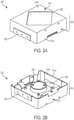
- FIG. 1A is a perspective view of an exterior of a flat panel antenna structure in accordance with some embodiments.
- FIG. 1B is a perspective view of an interior of the flat panel antenna structure of FIG. 1A in accordance with some embodiments.
- FIG. 1C is an exploded view of the interior of the flat panel antenna structure of FIG. 1B in accordance with some embodiments.
- the antenna structure 100 includes an antenna or radiator element 120 and a housing or enclosure 105 that protects the radiator element 120 from an operating environment.
- the radiator element 120 includes an array of elements characterized by array dimensions, such as a 2 N ⁇ 2 M element array where N and M are integers.
- the radiator element 120 may be formed in multiple layers via machining or casting.
- U.S. Patent No. 8,558,746 to Thomson et al. discusses a flat panel array antenna constructed as a series of different layers. Shown therein are flat panel arrays that include input, intermediate and output layers, with some embodiments including one or more slot layers and one or more additional intermediate layers.
- the radiator element 120 may utilize a corporate waveguide network and cavity couplers provided in stacked layers, and an output layer including cavity output ports, polarization rotator elements, and horn radiators that are machined in a monolithic structure, as described for example in U.S. Provisional Patent Application No. 62/308,436 entitled "FLAT PANEL ARRAYANTENNA WITH INTEGRATED POLARIZATION ROTATOR" to Biancotto et al.
- the radiator element 120 is secured to the enclosure 105 by various mounting hardware 140.
- the enclosure 105 and the mounting hardware 140 are designed or otherwise configured such that the radiator element 120 can be rotated within the enclosure 105 to adjust or alter a polarization thereof.
- the radiator element 120 may be configured to be rotated by about 90 degrees within the enclosure 105 in some embodiments.
- An interface plate 135 is secured to the radiator element 120 opposite to the front face 110 of the enclosure 105 by the mounting hardware 140.
- the interface plate 135 includes various structures that are designed or otherwise configured to mechanically secure and/or electrically connect the radiator element 120 to external telecommunications equipment, such as a customer radio.
- a mounting plate 130 is secured to the interface plate 135 and the radiator element 120 by the mounting hardware 140.
- the mounting plate 130 is configured to attach the enclosure 105 to a mounting bracket, such as the bracket 320 shown in FIG. 3B .
- the enclosure 105 includes a front face 110 that is positioned adjacent the radiating surface 120r of the radiator element 120, and sidewall surfaces 111 that house the radiator element 120 therebetween.
- the front face 110 includes an external or exterior surface 110a and an internal or interior surface 110b.
- the internal or interior surface may refer to the primary interior surface that defines the greatest thickness with respect to the opposite external or exterior surface.
- the sidewall surfaces 111 likewise include external or exterior surfaces 111a and internal or interior surfaces 111b, respectively.
- the enclosure 105 is a single-part radome-enclosure in which a radome portion 125 (illustrated with a dashed line) and the enclosure 105 are defined by a unitary member of a same material.
- the radome 125 is integrated with the front face 110 of the enclosure 105 using injection-molding techniques.
- the radome 125 which is positioned on or adjacent the radiating surface 120r of the radiator element 120, may be thinner than surrounding portions or areas of the front face 110 that are adjacent the sidewall surfaces 111 in some embodiments.
- an enclosure 105 including a thinner radome 125 (e.g., having a thickness of about 0.2 mm or less) than other portions of the front face 110 may allow for improved electrical performance as compared to a thicker radome 125 (e.g., having a thickness of about 1 mm) and/or an enclosure 105 where the radome 125 and the surrounding portions of the front face 110 have a same or uniform thickness (e.g., a thickness of about 4.5 mm).
- the thickness of the front face 110 may be defined between the external surface 110a and the internal surface 110b thereof, and may be stepped (as shown in FIGS. 4A-4E ) or tapered (as shown in FIGS.
- the radome portion 125 may also have a shape corresponding to the surface 120r of the radiator element 120, illustrated in FIGS. 1A-1C as a diamond-shape with beveled edges (thus defining an octagonal shape).
- radomes of other shapes which may or may not correspond to the shape of the surface 120r of the radiator element 120, are also included in embodiments described herein.
- radomes of other shapes which may or may not correspond to the shape of the surface 120r of the radiator element 120, are also included in embodiments described herein.
- other relative orientations between the radome 125 and the enclosure 105 e.g., 20 degrees, 30 degrees, etc. are included in embodiments described herein.
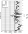
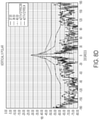
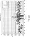
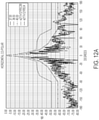
- FIGS. 7A-7D illustrate performance of the antenna structure 100 having a front face 110 including a 1.1 millimeter (mm) thick radome 125
- FIGS. 8A-8D illustrate performance of the antenna structure 100 having a front face 110 including a 0.24 millimeter (mm) thick radome 125, relative to desired envelopes e217v121R5C3B and e217v121R5C4.
- the e217v121R5C3B and e217v121R5C4 envelopes are ETSI Radiation Pattern Envelopes (RPEs), which the antenna radiation patterns should fall within or not cross in order to homologate the antenna as "ETSI Class 3" and "ETSI Class 4,” respectively.
- RPEs ETSI Radiation Pattern Envelopes
- both horizontal and vertical co-polarization characteristics are improved in the embodiments of FIGS. 8A and 8B as compared to the embodiments of FIGS. 7A and 7B , respectively.
- the radiation pattern improvement is given by 37.00, 38.50 and 40.00 measurements being suppressed below the e217v121R5C3B specification.
- horizontal and vertical cross-polarization characteristics are improved in the embodiments of FIGS.
- FIGS. 7A-7D and 8A -8D thus illustrate that performance of the radiator element 120 may be improved by reducing the thickness of the radome 125, thereby allowing the radiating surface 120r of the radiator element 120 to be positioned as close as possible to the external surface 110a of the enclosure 105 while still providing sufficient protection from conditions of the operating environment.
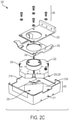
- FIG. 2A is a perspective view of an exterior of a flat panel antenna structure in accordance with some embodiments.
- FIG. 2B is a perspective view of an interior of the flat panel antenna structure of FIG. 2A in accordance with some embodiments.
- FIG. 2C is an exploded view of the interior of the flat panel antenna structure of FIG. 2B in accordance with some embodiments.
- the antenna structure 200 includes an antenna or radiator element 220 and housing or enclosure 205 that protects the radiator element 220 from an operating environment.
- the radiator element 220 may include monolithic and/or multiple layers that are formed via machining or casting.
- the radiator element 220 is secured to the enclosure 205 by various mounting hardware 240.
- the enclosure 205 and the mounting hardware 240 are designed or otherwise configured such that the radiator element 220 can be rotated within the enclosure 205 to adjust or alter a polarization thereof.
- the radiator element 220 may be configured to be rotated by about 90 degrees within the enclosure 205 in some embodiments.
- An interface plate 235 is secured to the radiator element 220 opposite to the front face 210 of the enclosure 205 by the mounting hardware 240.
- the interface plate 235 includes various structures that are designed or otherwise configured to mechanically secure and/or electrically connect the radiator element 220 to external telecommunications equipment, such as a customer radio.
- a mounting plate 230 is secured to the interface plate 235 and the radiator element 220 by the mounting hardware 240.
- the mounting plate 230 is configured to attach the enclosure 205 to a mounting bracket, such as the bracket 320 shown in FIG. 3B .
- the enclosure 205 includes a front face 210 that is positioned adjacent the radiating surface 220r of the radiator element 220, and sidewall surfaces 211 that house the radiator element 220 therebetween.
- the front face 210 includes an external or exterior surface 210a and an internal or interior surface 210b.
- the internal or interior surface may refer to the primary interior surface having the greatest thickness with respect to the opposite external or exterior surface.
- the sidewall surfaces 211 likewise include external or exterior surfaces 211a and internal or interior surfaces 211b, respectively.
- the enclosure 205 is a two-part radome-enclosure including a radome 225 that is a separate or distinct component from the enclosure 205.
- the radome 225 is a thin layer or film that is attached to the radiating surface 220r of the radiator element 220.
- the enclosure 205 includes an opening 226 between the interior surface 210b and the exterior surface 210a of the front face 210.
- the opening 226 is sized and shaped to expose at least a portion of the surface 220r of the radiator element 220 that includes the radome 225 thereon.
- one or more dimensions of the opening 226 in the enclosure 205 may be smaller than one or more dimensions of the surface 220r of the radiator element 220, such that the radome 225 thereon is recessed relative to the external surface 210a of the front face 210 of the enclosure 205.
- the opening 226 may have the same or larger dimensions than the surface 220r of the radiator element, and thus, in some embodiments, the radome 225 may be coplanar with or protrude from the external surface 210a of the front face 210 of the enclosure.
- the thickness of the radome 225 is less than a thickness of the front face 210 of the enclosure, as defined between the external surface 210a and the internal surface 210b thereof.
- the use of a thinner radome 225 (e.g., about 0.1-0.5 mm) for environmental protection of the radiator element 220 can reduce or avoid disruption of the electrical performance of the radiator element 220, while the thicker enclosure 205 (e.g., about 4.5 mm or more) can provide sufficient structural strength and/or rigidity to support the radiating element 220 and/or other components housed within the enclosure 205.
- the radome thickness may vary according to frequency of operation of the radiator element 220.
- the radome 225 and the enclosure 205 may be formed of the same or different materials, by the same or different processes.
- the radome 225 and the enclosure 205 may be formed of a plastic material; however, the radome 225 may be formed via an extrusion process, while the enclosure 205 may be formed via an injection molding process.
- the radome 225 may be formed of a flexible material, such as an ultraviolet (UV)-stable polymer, while the enclosure 205 may be formed from a rigid material.
- the radome 225 may be attached to the radiating surface 220r of the radiator element 220 using glue or tape in some embodiments.
- the radiator element 220 may thus be secured to the enclosure 205 using the mounting hardware 240, such that the radome 225 itself is not physically attached to the front face 210 of enclosure 205.
- the thickness of the front face 210 may be defined between the external surface 210a and the internal surface 210b thereof, and may be stepped (as shown in FIGS. 4A-4E ) or tapered (as shown in FIGS. 5A-5E ) between the internal surface 210b and the external surface 210a in some embodiments to further improve performance.
- portions of the front face 210 adjacent the sidewall surfaces 211 may have a greater thickness (e.g., a thickness of about 4.5 mm or more), and a portion of the front face 210 surrounding the opening 226 or bordering and/or overlapping the surface 220r of the radiator element may be stepped or tapered to a reduced thickness (e.g., a thickness of about 1.5 mm or less).
- the radome 225 is likewise thinner than the portions of the front face 210 surrounding the opening 226.
- Embodiments in which the front face 210 includes portions of different thicknesses allows the radiator element 220 (including the radome 225 attached to the surface 220r thereof) to protrude beyond the internal surface 210b of the enclosure and be positioned closer to the external surface 210a of the front face 210, thereby improving radiation performance.
- the opening 226 and/or radome 225 may also have a shape similar or corresponding to the surface 220r of the radiator element 220.
- the opening 226 exposing the radome 225 has a diamond-shape with rounded edges, while the surface 220r of the radiator element 220 has a diamond-shape with beveled edges.
- radomes and/or openings 226 of other shapes which may or may not correspond to the shape of the surface 220r of the radiator element 220, are also included in embodiments described herein.
- opening 226 and/or radome 225 are rotated by about 45 degrees relative to the enclosure 205, it will be understood that other relative orientations between the opening 226/radome 225 and the enclosure 205 (e.g., 20 degrees, 30 degrees, etc.) are included in embodiments described herein.
- FIG. 3A is a perspective view of a telecommunications device including the flat panel antenna structure of FIG. 2A attached to a user or customer equipment
- FIG. 3B is a front view of the telecommunications device including the flat panel antenna structure of FIG. 3A as attached to a mounting bracket.
- the telecommunications device 300 includes the antenna structure 200, which is a two-part design including an enclosure 205 having a front face 210 and a radome 225 that is recessed relative to the external surface 210a of the front face 210.
- the radome 225 may be coplanar with or protruding from the external surface 210a of the front face 210 in some embodiments.
- FIG. 3A further illustrates attachment of the antenna structure 200 to customer equipment, illustrated as a customer radio 310.
- the enclosure 205 is designed or otherwise configured such that the sidewalls 211 thereof are aligned with corresponding sidewalls 311 of the customer radio 310. The color and/or other aesthetic aspects of the enclosure 205 may also be matched to those of the customer radio 310.
- the enclosure 205 is configured to mate with or is otherwise mechanically compatible with attachment points on the customer radio 310.
- the attachment points of the interface plate 235 shown in the exploded view of FIG. 2C are sized and configured to align with corresponding attachment points on the customer radio 310, such that the antenna structure 200 can be secured to the customer radio 310 by the mounting hardware 240.
- the radiator element 220 within the enclosure 205 is likewise configured for electrical connection to one or more components of the customer radio 310. More generally, the physical, electrical, and/or aesthetic design of the antenna structure 200 and enclosure 205 may match or closely correspond to that of the customer radio 310.
- FIG. 3B further illustrates attachment of the telecommunications device 300 to a mounting bracket 320.
- the enclosure 205 is attached to the mounting bracket 320 via attachment points on the mounting plate 230 shown in the exploded view of FIG. 2C .
- the attachment points on the mounting plate 230 are sized and configured to align with corresponding attachment points on the mounting bracket 320, such that the antenna structure 200 can be secured to the mounting bracket 320 by mounting hardware 340.
- FIG. 3B with reference to attachment of the enclosure 205 to the mounting bracket 320 by way of example, it will be understood that additional and/or alternative attachments to the mounting bracket 320 may be provided.
- the attachment of the telecommunications device 300 to the mounting bracket 320 may be implemented by attachment points on the customer radio 310, rather than or in addition to those of the mounting plate 230 of the antenna structure 200.
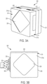
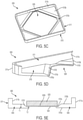
- FIGS. 4A-4E are various views illustrating the front face of a flat panel antenna enclosure in accordance with some embodiments.
- the front face 410 of the enclosure 405 includes an exterior or external surface 410a that is bounded by outer surfaces 411a of sidewalls 411.
- the front face 410 includes an opening 426 extending therethrough from the external surface 410a to the internal surface 410b.
- the opening 426 has a shape corresponding to the shape of an antenna or radiator element to be housed in the enclosure 405.
- the opening 426 is shaped according to the shape of the radiator element 120 of FIGS.
- FIG. 4B further illustrates the shape of the opening 426 in front view. As shown in FIG. 4B , the opening 426 may not be centered on the front face 410 of the enclosure 405, but rather, may be shifted toward one or more of the sidewall surfaces 411.
- FIG. 4C and FIG. 4D illustrate the interior of the enclosure 405, and in particular, the internal surface 410b that is opposite to the external surface 410a illustrated in FIGS. 4A and 4B .
- the inner or internal surface 410b of the front face 410 is bounded by inner surfaces 411b of the sidewalls 411.
- the opening 426 in the front face 410 extends from the external surface 410a to the internal surface 410b.
- a thickness of the front face 410 (as defined between the external surface 410a and the internal surface 410b) may be non-uniform in some embodiments.
- a uniformly thick front face 410 of the enclosure 405 may negatively affect performance (e.g., radiation patterns) of a radiator element that is positioned adjacent the front face 410 within the enclosure 405, embodiments described herein provide a front face 410 having a greater thickness T1 between the external surface 410a and the internal surface portion 410b adjacent the sidewall surfaces 411, and a lesser thickness T2 between the external surface 410a and an internal surface portion 410c adjacent or surrounding the opening 426, as shown in greater detail in the cross-sectional view of FIG. 4E .
- the antenna structure 400 includes an antenna or radiator element 420 that is housed within the sidewall surfaces 411 and adjacent the front face 410 of the enclosure 405.
- a protective radome 425 is attached or otherwise provided on a radiating surface 420r of the radiator element 420.
- the opening 426 in the front face 410 is sized to expose the surface 420r of the radiator element 420 that includes the radome 425 thereon.
- the dimensions of the opening 426 are smaller than the dimensions of the surface 420r of the radiator element 420, such that a portion 410c of the internal surface 410b of the front face 410 overlaps with edges of the radome 425, defining a border around the perimeter of the radiating surface 420r of the radiator element 420.
- the surface 420r of the radiator element 420 including the radome 425 thereon is recessed relative to the external surface 410a of the front face 410 of the enclosure 405.
- the opening 426 may have the same or larger dimensions than the surface 420r of the radiator element 420, and thus, the radome 425 may be coplanar with or protrude beyond the external surface 410a of the front face 410 of the enclosure 405.
- the front face 410 of the enclosure 405 thus includes areas having a non-uniform or varying thickness, where a thickness T1 (between the external surface 410a and the internal surface 410b adjacent the sidewall surfaces 411) differs from a thickness T2 (between the external surface 410a and the internal surface 410c adjacent or surrounding the opening 426).
- a thickness T1 between the external surface 410a and the internal surface 410b adjacent the sidewall surfaces 4111
- the thickness T2 between the external surface 410a and the internal surface 410c adjacent or surrounding the opening 426.
- the thickness T1 of the front face 410 adjacent the sidewall surfaces 411 may be about 4.5 mm or more to provide the enclosure 405 with sufficient structural rigidity to provide environmental protection of the radiator element 420
- the thickness T2 of the front face 410 adjacent the opening 426 may be about 1.5 mm or less to allow for sufficient radiative performance of the radiator element 420.
- a stepped portion 410s is thereby defined at an interface between the internal surface 410b and the internal surface 410c over the thickness of the front face 410 of the enclosure, due to the differing thicknesses T1 and T2.
- This step difference 410s allows the radiating surface 420r of the radiator element 420 to be positioned closer to the external surface 410a of the front face 410 of the enclosure, which may improve radiative performance.
- the radome 425 on the radiating surface 420r of the radiator element 420 may have a thickness that is less than the thickness T2.
- the radome 425 may be an extruded plastic thin film, while the enclosure 405 may be injection-molded plastic.
- the radome 425 and the enclosure 405 may be formed of different materials in some embodiments. Also, the amount of overlap between the internal surface 410c and the perimeter of the radiating surface 420r is shown for purposes of illustration only, and may be reduced or increased to provide improved or optimal performance of the radiator element 420.
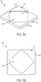
- FIGS. 5A-5E are various views illustrating the front face of a flat panel antenna enclosure in accordance with some embodiments, such as those shown in FIGS. 2A-2C and 3A -3B .
- the front face 510 of the enclosure 505 includes an exterior or external surface 510a that is bounded by outer surfaces 511a of sidewalls 511.
- the front face 510 includes a diamond-shaped opening 526 extending therethrough from the external surface 510a to the internal surface 510b.
- the opening 526 may have a shape corresponding or similar to the shape of an antenna or radiator element to be housed in the enclosure 505; however, it will be understood the opening 526 may also be shaped differently from that of the radiator element to be housed therein.
- FIG. 5B further illustrates the shape of the opening 526 in front view. As shown in FIG. 5B , the opening 526 may not be centered on the front face 510 of the enclosure 505, but may be shifted toward one or more of the sidewall surfaces 511.
- FIG. 5C and FIG. 5D illustrate the interior of the enclosure 505, and in particular, the internal surface 510b of the front face 510, which is opposite to the external surface 510a illustrated in FIGS. 5A and 5B .
- the inner or internal surface 510b of the front face 510 is bounded by inner surfaces 511b of the sidewalls 511.
- the opening 526 in the front face 510 extends from the external surface 510a to the internal surface 510b.
- a thickness of the front face 510 (as defined between the external surface 510a and the internal surface 510b) is non-uniform; however, in contrast to the step difference 410s shown in the embodiments of FIGS. 4A-4E (which may be impractical to implement in some manufacturing processes where substantial variation of polymer thickness may be difficult to achieve), embodiments described herein provide a front face 510 having a thickness that tapers from a greater thickness T1 (between the external surface 510a and the internal surface portion 510b adj acent the sidewall surfaces 511) to a lesser thickness T2 (between the external surface 510a and an internal surface portion 510c adjacent or surrounding the opening 426), as shown in greater detail in the cross-sectional view of FIG. 5E .
- the antenna structure 500 includes an antenna or radiator element 520 that is housed within the sidewall surfaces 511 and adjacent the front face 510 of the enclosure 505.
- a protective radome 525 is attached or otherwise provided on a radiating surface 520r of the radiator element 520.
- the opening 526 in the front face 510 is sized to expose the surface 520r of the radiator element 520 that includes the radome 525 thereon.
- the dimensions of the opening 526 are smaller than the dimensions of the surface 520r of the radiator element 520, such that a portion 510c of the internal surface 510b of the front face 510 overlaps with edges of the radome 525, defining a border around the perimeter of the radiating surface 520r of the radiator element 520.
- the surface 520r of the radiator element 520 including the radome 525 thereon is thus recessed relative to the external surface 510a of the front face 510 of the enclosure 505.
- the opening 526 may have the same or larger dimensions than the surface 520r of the radiator element 520, and thus, the radome 525 may be coplanar with or protrude beyond the external surface 510a of the front face 510 of the enclosure 505 in some embodiments.
- the front face 510 of the enclosure 505 includes areas having a non-uniform or varying thickness, where a thickness T1 (between the external surface 510a and the internal surface 510b in the area adjacent the sidewall surfaces 511) differs from a thickness T2 (between the external surface 510a and the internal surface 510c adjacent the opening 526).
- the thickness T1 of the front face 510 adjacent the sidewall surfaces 511 may be selected or otherwise configured to provide the enclosure 505 with sufficient structural rigidity for environmental protection of the radiator element 520, while the thickness T2 of the front face 510 adjacent the opening 526 may be selected or otherwise configured so as not reduce or avoid negative effects on the radiative performance of the radiator element 520.
- a sloped or tapered portion 510t is thereby defined at an interface between the internal surface 510b and the internal surface 510c over the thickness of the front face 510 of the enclosure.
- the tapered portion 510t may taper linearly and/or non-linearly (i.e., may include straight and/or curved/rounded areas) in some embodiments.
- the smaller thickness T2 adjacent the opening 526 allows the radiating surface 520r of the radiator element 520 to be positioned closer to the external surface 510a than the internal surface 510b of the front face 510 of the enclosure, which may improve radiative performance.
- the tapered portion 510t between the areas 510b, 510c of different thicknesses T1, T2 may be easier to manufacture in comparison to the stepped portion 410s shown in FIGS. 4A-4E .
- the radome 525 on the radiating surface 520r of the radiator element 520 may have a thickness that is less than the thickness T2, and may be formed of the same or a different material than the enclosure 505. Also, the amount of overlap between the internal surface 510c and the perimeter of the radiating surface 520r is shown for purposes of illustration only, and may be reduced or increased to provide improved or optimal performance of the radiator element 520.
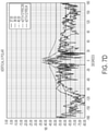
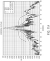
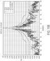
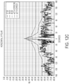
- FIGS. 9A-9D illustrate performance of the antenna structure 400 having a front face 410 including a stepped thickness in cross-section
- FIGS. 10A-10D illustrate performance of the antenna structure 500 having a front face 510 including a tapered thickness in cross-section
- the enclosure is a machined-from-solid enclosure with glued additional components. As shown in FIGS.
- FIGS. 9A , 9B , 10A , and 10B horizontal and vertical co-polarization characteristics of the embodiments of FIGS. 9A and 9B are substantially similar to the embodiments of FIGS. 10A and 10B , respectively.
- FIGS. 9C , 9D , 10C , and 10D horizontal and vertical cross-polarization characteristics of the embodiments of FIGS. 9C and 9D are substantially similar to the embodiments of FIGS. 10C and 10D , respectively.
- FIGS. 9C , 9D , 10C , and 10D horizontal and vertical cross-polarization characteristics of the embodiments of FIGS. 9C and 9D are substantially similar to the embodiments of FIGS. 10C and 10D , respectively.
- embodiments of enclosures described herein having stepped front face cross-sections may offer performance similar to embodiments of enclosures described herein having tapered front face cross-sections, as both of such embodiments allow for positioning of the radiating surface of the radiator element very close to (or protruding beyond) the exterior surface of the front face of the enclosure.
- embodiments having front faces with tapered thicknesses are free of abrupt changes in thickness, such embodiments may be preferable from a manufacturing standpoint as compared to embodiments having front faces with stepped thicknesses.
- FIGS. 6A, 6B, and 6C are views of an interior of a flat panel antenna enclosure formed from a non-conductive material (such as injection-molded plastic) and further including metallized sidewall surfaces in accordance with some embodiments, which may offer improved performance.
- a non-conductive material such as injection-molded plastic
- FIGS. 6A-6C the internal surface 610b of the front face of the enclosure 605 is bounded by inner sidewall surfaces 611b, and an opening 626 extends through the front face from the internal surface 610b to an external surface of the enclosure 605.
- the opening 626 is sized and configured to expose or accept a radome that is attached to a radiating surface of a radiator element, such as the radome 525 that is attached to the radiating surface 520r of the radiator element 520 in the embodiment of FIGS. 5A-5E .
- a sloped or tapered portion 610t (similar to the portion 510t of FIG. 5E ) is defined over the thickness of the front face 610 of the enclosure, between the internal surface 610b adjacent the sidewall surfaces 611b and an internal surface 610c adjacent the opening 626.
- the front face of the enclosure 605 includes a non-uniform or varying thickness, allowing a radiating surface of a radiator element to be positioned closer to the external surface of the front face of the enclosure 605.
- some embodiments described herein may further include one or more metal layers 650 on one or more of the inner sidewall surfaces 611b of the enclosure 605.
- respective metal layers 650 are implemented using aluminum strips or tape on opposite inner sidewall surfaces 611b of the enclosure; however, it will be understood that the metal layers 650 may be implemented using other metals and/or materials in some embodiments.
- other forms or types of metallization including , but not limited to electro(less) plating, Electrodag ® coating, metal paint, etc.
- the metal layers 650 may be confined to or embedded within the sidewall surfaces 611b in some embodiments.
- the metal layers 650 are respectively provided on particular opposing sidewall surfaces 611b that correspond to the azimuth plane of the radiator element housed within the enclosure 605. That is, when the antenna structure (including the enclosure 605 and internal radiator element) is mounted or otherwise employed in a telecommunications device or apparatus, the metal layers 650 are provided on the sidewall surfaces 611b that are oriented to affect the azimuth angle of the desired antenna coverage pattern. Additionally or alternatively, it will be understood that metal layers 650 can be included on opposing sidewall surfaces 611b of the enclosure 605 that are oriented to affect the elevation angle/correspond to the elevation plane of the radiator element in some embodiments.
- the metal layers 650 need not extend along a majority or entirety of the opposing sidewall surfaces 611b. Rather, improvements in the radiating pattern of the radiator element may be achieved in some embodiments by positioning the metal layers 650 adjacent or closest to edge portions of the radiator element.
- the opening 626 is designed to correspond to the shape of the radiator element to be included in the enclosure 605; thus, in the illustrated embodiments, the metal layers 650 may be positioned adjacent to (or in some embodiments, may be confined to) corner portions 626c of the opening 626 in the front face of the enclosure 605.
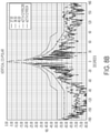
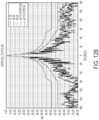
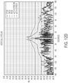
- FIGS. 11A-11D and 12A -12D Some performance characteristics of antenna structures including two-part radomeenclosures are illustrated in the graphs of FIGS. 11A-11D and 12A -12D over a ⁇ 180 degree azimuth angle range.
- FIGS. 11A-11D illustrate performance of the antenna structure having a front face including a tapered thickness in cross-section (such as the structure 505 of FIG. 5A-5E )
- FIGS. 12A-12D illustrate performance of the antenna structure having a front face including a tapered thickness in cross-section along with metal layers on internal sidewall surfaces that are oriented to affect the azimuth angle (such as the structure 605 of FIG. 6A-6C ).
- the enclosures are a single piece injection molded enclosure.
- the inclusion of the metal layers on the opposing internal sidewall surfaces of the enclosure corresponding to the azimuth plane of the antenna structure may offer improved performance in the 100-120 degree region where measured radiation patterns are made compliant to the desired specification e217v121R5C3B, as compared to the antenna structure FIGS. 11A-11D , which does not include the metal layers.
- FIGS. 11A , 11B , 12A , and 12B horizontal and vertical co-polarization characteristics are improved in the embodiments of FIGS. 12A and 12B as compared to the embodiments of FIGS. 11A and 11B , respectively.
- FIGS. 11A , 11B , 12A , and 12B horizontal and vertical co-polarization characteristics are improved in the embodiments of FIGS. 12A and 12B as compared to the embodiments of FIGS. 11A and 11B , respectively.
- the horizontal and vertical cross-polarization characteristics of the embodiments of FIGS. 12C and 12D are improved as compared to the horizontal and vertical cross-polarization graphs of FIGS. 11C and 11D , respectively.
- the inclusion of the metal layers in one or more of the sidewall surfaces of the enclosure may offer further improvements in radiative performance.
- embodiments of the present invention provide a high performance flat panel antenna with a front face having a non-uniform or varying cross-sectional thickness that is strong, lightweight and may be repeatedly cost efficiently manufactured with a very high level of precision.
Landscapes
- Details Of Aerials (AREA)
- Aerials With Secondary Devices (AREA)
Claims (15)
- Structure d'antenne, comprenant :un élément rayonnant (120) comprenant un réseau d'éléments d'antenne ; etune enceinte (105) comprenant l'élément rayonnant (120) à l'intérieur, l'enceinte (105) comprenant une face avant (110) qui est adjacente à une surface de l'élément rayonnant (120) et des surfaces de paroi latérale (111) qui logent l'élément rayonnant (120) entre celles-ci, et une plaque d'interface (235) configurée pour accepter un matériel de montage qui fixe l'enceinte (105) à un équipement de télécommunications externe,dans laquelle la face avant (110) de l'enceinte (105) comprend une surface interne (210b) qui est délimitée par les surfaces de paroi latérale (111) et une surface externe (210a) à l'opposé de la surface interne (210b), dans laquelle la surface de l'élément rayonnant (120) est positionnée plus près de la surface externe (210a) que de la surface interne (210b) de la face avant (110) de l'enceinte (105).
- Structure d'antenne selon la revendication 1, dans laquelle les surfaces externe et interne (210 a-b) définissent une épaisseur de la face avant (110) qui varie entre elles.
- Structure d'antenne selon la revendication 2, dans laquelle l'épaisseur de la face avant (110) comprend une première épaisseur adjacente aux surfaces de paroi latérale (111) et une deuxième épaisseur adjacente à la surface de l'élément rayonnant (120), dans laquelle la première épaisseur est supérieure à la deuxième épaisseur.
- Structure d'antenne selon la revendication 3, dans laquelle la face avant (110) comprend une partie étagée (410) entre la première épaisseur et la deuxième épaisseur.
- Structure d'antenne selon la revendication 3, dans laquelle la face avant (110) comprend une partie conique ou biseautée entre la première épaisseur et la deuxième épaisseur.
- Structure d'antenne selon l'une quelconque des revendications précédentes, dans laquelle la face avant (110) comprend une partie de radôme intégrale (125) ayant la deuxième épaisseur adjacente à la surface de l'élément rayonnant (120).
- Structure d'antenne selon l'une quelconque des revendications 1-5, dans laquelle la face avant (110) de l'enceinte (105) comprend une ouverture s'étendant à travers celle-ci à partir de la surface externe (210a) jusqu'à la surface interne (210b), et comprenant en outre :
un radôme (125), distinct de l'enceinte (105), sur la surface de l'élément rayonnant (120) et au moins partiellement exposé par l'ouverture, le radôme (125) ayant une épaisseur qui est inférieure à l'épaisseur maximale de la face avant (110) de l'enceinte (105). - Structure d'antenne selon la revendication 7, dans laquelle le radôme (125) comprend un matériau différent de celui de l'enceinte (105).
- Structure d'antenne selon les revendication 7 ou 8, dans laquelle la surface de l'élément rayonnant (120) comprenant le radôme (125) sur celle-ci est en retrait par rapport à la surface externe (210a) de la face avant (110) de l'enceinte (105).
- Structure d'antenne selon l'une quelconque des revendications 7-9, dans laquelle la face avant (110) comprend une partie de bordure ayant la deuxième épaisseur adjacente à un bord de l'ouverture, dans laquelle la partie de bordure chevauche un périmètre du radôme (125).
- Structure d'antenne selon les revendications 7 ou 8, dans laquelle la surface de l'élément rayonnant (120) comprenant le radôme (125) sur celle-ci est coplanaire avec ou fait saillie au-delà de la surface externe (210a) de la face avant (110) de l'enceinte (105).
- Structure d'antenne selon l'une quelconque des revendications précédentes, dans laquelle l'enceinte (105) comprend un matériau non conducteur, et comprenant en outre :
un élément métallisé adjacent à un bord de la surface de l'élément rayonnant (120). - Structure d'antenne selon la revendication 12, dans laquelle l'élément métallisé comprend des couches métalliques respectives sur des surfaces opposées parmi les surfaces de paroi latérale (111) de l'enceinte (105),
éventuellement dans laquelle les surfaces opposées parmi les surfaces de paroi latérale (111) comprenant les couches métalliques respectives sur celles-ci sont orientées pour affecter l'angle d'azimut d'un motif de couverture de l'élément rayonnant (120). - Structure d'antenne selon l'une quelconque des revendications précédentes, dans laquelle l'élément rayonnant (120) peut tourner à l'intérieur de l'enceinte (105) pour modifier une polarisation de signaux transmis par l'élément rayonnant (120).
- Structure d'antenne selon l'une quelconque des revendications précédentes, dans laquelle l'élément rayonnant comprend une antenne hyperfréquence de Classe 3 ou de Classe 4 de l'Institut Européen des Normes de Télécommunications (ETSI).
Applications Claiming Priority (2)
| Application Number | Priority Date | Filing Date | Title |
|---|---|---|---|
| US201662430654P | 2016-12-06 | 2016-12-06 | |
| PCT/US2017/060846 WO2018106401A2 (fr) | 2016-12-06 | 2017-11-09 | Enceintes de radôme d'antenne et structures d'antenne associées |
Publications (3)
| Publication Number | Publication Date |
|---|---|
| EP3552272A2 EP3552272A2 (fr) | 2019-10-16 |
| EP3552272A4 EP3552272A4 (fr) | 2020-07-08 |
| EP3552272B1 true EP3552272B1 (fr) | 2022-03-23 |
Family
ID=62240673
Family Applications (1)
| Application Number | Title | Priority Date | Filing Date |
|---|---|---|---|
| EP17878481.5A Not-in-force EP3552272B1 (fr) | 2016-12-06 | 2017-11-09 | Enceintes de radôme d'antenne et structures d'antenne associées |
Country Status (4)
| Country | Link |
|---|---|
| US (1) | US10651551B2 (fr) |
| EP (1) | EP3552272B1 (fr) |
| CN (1) | CN109997279B (fr) |
| WO (1) | WO2018106401A2 (fr) |
Families Citing this family (11)
| Publication number | Priority date | Publication date | Assignee | Title |
|---|---|---|---|---|
| ES2951209T3 (es) * | 2018-01-10 | 2023-10-18 | Zanini Auto Grup Sa | Radomo para vehículos |
| JP1621594S (fr) * | 2018-02-02 | 2019-01-07 | ||
| US11165146B2 (en) * | 2018-08-28 | 2021-11-02 | Commscope Technologies Llc | Base station antenna radomes with non-uniform wall thickness |
| DE102019204700A1 (de) * | 2019-04-02 | 2020-10-08 | Brose Fahrzeugteile Se & Co. Kommanditgesellschaft, Bamberg | Radarvorrichtung, Verfahren zum Herstellen einer Radarvorrichtung und Kraftfahrzeug |
| KR102674840B1 (ko) * | 2019-12-20 | 2024-06-13 | 삼성전자 주식회사 | 무선 통신 시스템에서 안테나의 최적 빔 구현을 위한 커버 장치 |
| CN111430901B (zh) * | 2020-01-17 | 2022-04-12 | 上海阿莱德实业股份有限公司 | 5g基站用集天线于一体的天线罩及其制备方法 |
| KR102747648B1 (ko) * | 2020-04-21 | 2024-12-27 | 삼성전자주식회사 | 레이돔을 포함하는 안테나 장치 및 이를 포함하는 기지국 |
| USD973040S1 (en) * | 2020-11-06 | 2022-12-20 | Lite-On Electronics (Guangzhou) Limited | Antenna monitoring tool box |
| WO2023059024A1 (fr) * | 2021-10-07 | 2023-04-13 | 엘지이노텍 주식회사 | Dispositif radar et son procédé de commande |
| US20230170608A1 (en) * | 2021-11-30 | 2023-06-01 | Corning Research & Development Corporation | Radome cover design for beamforming antenna |
| CN114361785B (zh) * | 2021-12-08 | 2025-08-19 | 武汉中元通信股份有限公司 | 一种展宽波束的微带天线结构 |
Family Cites Families (30)
| Publication number | Priority date | Publication date | Assignee | Title |
|---|---|---|---|---|
| US4191959A (en) * | 1978-07-17 | 1980-03-04 | The United States Of America As Represented By The Secretary Of The Army | Microstrip antenna with circular polarization |
| JP2003140773A (ja) * | 2001-10-31 | 2003-05-16 | Toshiba Corp | 無線通信デバイスおよび情報処理装置 |
| JP2004077399A (ja) * | 2002-08-22 | 2004-03-11 | Hitachi Ltd | ミリ波レーダ |
| EP1601046B1 (fr) | 2004-05-28 | 2008-07-02 | Huber + Suhner Ag | antenne réseau comportant un boîtier |
| CN101022184A (zh) * | 2006-02-13 | 2007-08-22 | 诠欣股份有限公司 | 具有共构天线的无线通讯产品机壳 |
| US7619571B2 (en) * | 2006-06-28 | 2009-11-17 | Nokia Corporation | Antenna component and assembly |
| KR100946975B1 (ko) * | 2008-08-18 | 2010-03-15 | 재단법인 광양만권 유아이티연구소 | 패치 안테나 장착 구조체 |
| US9905922B2 (en) * | 2011-08-31 | 2018-02-27 | Qualcomm Incorporated | Wireless device with 3-D antenna system |
| US8558746B2 (en) | 2011-11-16 | 2013-10-15 | Andrew Llc | Flat panel array antenna |
| USD655278S1 (en) | 2011-11-16 | 2012-03-06 | Andrew Llc | 12-sided flat panel array antenna |
| USD654910S1 (en) | 2011-11-16 | 2012-02-28 | Andrew Llc | 10-sided flat panel array antenna |
| USD653654S1 (en) | 2011-11-16 | 2012-02-07 | Andrew Llc | 8-sided flat panel array antenna |
| JP5953969B2 (ja) * | 2012-06-14 | 2016-07-20 | 株式会社デンソー | レーダ装置 |
| USD732472S1 (en) | 2012-08-20 | 2015-06-23 | Amazon Technologies, Inc. | Power adapter |
| US9979078B2 (en) * | 2012-10-25 | 2018-05-22 | Pulse Finland Oy | Modular cell antenna apparatus and methods |
| CA151747S (en) | 2013-01-23 | 2014-04-29 | Nec Corp | Wireless communication repeater |
| US9531067B2 (en) | 2013-02-08 | 2016-12-27 | Ubiquiti Networks, Inc. | Adjustable-tilt housing with flattened dome shape, array antenna, and bracket mount |
| US9647338B2 (en) | 2013-03-11 | 2017-05-09 | Pulse Finland Oy | Coupled antenna structure and methods |
| USD716752S1 (en) | 2013-05-21 | 2014-11-04 | Panasonic Corporation | Wireless communication base station |
| USD705748S1 (en) | 2013-09-14 | 2014-05-27 | Shenzhen Xin Ni Da Technology Co., Ltd | Bluetooth receiver |
| USD768607S1 (en) | 2014-01-02 | 2016-10-11 | Lutron Electronics Co., Inc. | Wireless control device |
| JP6402774B2 (ja) * | 2014-10-16 | 2018-10-10 | 株式会社村田製作所 | アンテナモジュール収納構造 |
| CN105792560B (zh) * | 2014-12-24 | 2020-01-31 | 深圳富泰宏精密工业有限公司 | 壳体、应用该壳体的电子装置及其制作方法 |
| USD785608S1 (en) | 2015-02-02 | 2017-05-02 | Eero Inc. | Router |
| USD797100S1 (en) | 2015-02-20 | 2017-09-12 | Robert Bosch Gmbh | Apparatus for recording, transmission or processing of information |
| JP1543628S (fr) | 2015-07-13 | 2017-02-06 | ||
| USD776657S1 (en) | 2015-10-02 | 2017-01-17 | Savant Systems, Llc | Controller for home automation |
| USD790538S1 (en) | 2016-01-15 | 2017-06-27 | Sharp Kabushiki Kaisha | Wireless access point |
| CN108475852A (zh) | 2016-03-15 | 2018-08-31 | 康普技术有限责任公司 | 具有集成极化旋转器的平板阵列天线 |
| USD794020S1 (en) | 2016-06-15 | 2017-08-08 | Comcast Cable Communications, Llc | Cable modem |
-
2017
- 2017-11-09 EP EP17878481.5A patent/EP3552272B1/fr not_active Not-in-force
- 2017-11-09 US US15/808,252 patent/US10651551B2/en not_active Expired - Fee Related
- 2017-11-09 CN CN201780072712.6A patent/CN109997279B/zh not_active Expired - Fee Related
- 2017-11-09 WO PCT/US2017/060846 patent/WO2018106401A2/fr not_active Ceased
Also Published As
| Publication number | Publication date |
|---|---|
| EP3552272A2 (fr) | 2019-10-16 |
| US20180159211A1 (en) | 2018-06-07 |
| US10651551B2 (en) | 2020-05-12 |
| CN109997279B (zh) | 2021-09-03 |
| WO2018106401A2 (fr) | 2018-06-14 |
| EP3552272A4 (fr) | 2020-07-08 |
| CN109997279A (zh) | 2019-07-09 |
| WO2018106401A3 (fr) | 2018-07-26 |
Similar Documents
| Publication | Publication Date | Title |
|---|---|---|
| EP3552272B1 (fr) | Enceintes de radôme d'antenne et structures d'antenne associées | |
| US12362461B2 (en) | Base station antennas having at least one grid reflector and related devices | |
| US7026993B2 (en) | Planar antenna and array antenna | |
| US6911939B2 (en) | Patch and cavity for producing dual polarization states with controlled RF beamwidths | |
| US6911956B2 (en) | Array antenna | |
| US10056701B2 (en) | Multiband WiFi directional antennas | |
| US20080252552A1 (en) | Antenna Housing and Antennas with Such Antenna Housings | |
| US6285323B1 (en) | Flat plate antenna arrays | |
| EP1860731B1 (fr) | Module d'antenne plane, antenne a reseau planaire triple, et convertisseur a guide d'ondes lineaire triple | |
| US7245267B2 (en) | Mobile radio antenna radome with integral reflector | |
| CA2250292C (fr) | Reseau d'antennes planes | |
| EP1783516B1 (fr) | Appareil pour alignement des micro-ondes | |
| US20240145905A1 (en) | Base station antennas having light weight multi-layer composite frequency selective surfaces | |
| US20230395987A1 (en) | Base station antennas having at least one grid reflector and related devices | |
| US12562482B2 (en) | Arrays with three-dimensional conformal radiating elements | |
| EP0312989B1 (fr) | Antenne à micro-ondes | |
| CN212626051U (zh) | 天线结构 | |
| US12469960B2 (en) | Base station antennas | |
| US7355555B2 (en) | Antenna | |
| JP4858575B2 (ja) | 放送受信用アンテナ装置 | |
| Hofmann et al. | A 3D Printed Quad-Ridged Flared Horn Antenna Feeder for Radio-Telescopes | |
| US11749897B2 (en) | Slot antenna assembly with tapered feedlines and shaped aperture | |
| CN117832869A (zh) | 智能反射装置 | |
| MXPA03007355A (es) | Metodo y sistema para producir estados de polarizacion dual con anchos de haz de rf controlados. | |
| CN117832870A (zh) | 反射组件及具有其的天线 |
Legal Events
| Date | Code | Title | Description |
|---|---|---|---|
| STAA | Information on the status of an ep patent application or granted ep patent |
Free format text: STATUS: THE INTERNATIONAL PUBLICATION HAS BEEN MADE |
|
| PUAI | Public reference made under article 153(3) epc to a published international application that has entered the european phase |
Free format text: ORIGINAL CODE: 0009012 |
|
| STAA | Information on the status of an ep patent application or granted ep patent |
Free format text: STATUS: REQUEST FOR EXAMINATION WAS MADE |
|
| 17P | Request for examination filed |
Effective date: 20190528 |
|
| AK | Designated contracting states |
Kind code of ref document: A2 Designated state(s): AL AT BE BG CH CY CZ DE DK EE ES FI FR GB GR HR HU IE IS IT LI LT LU LV MC MK MT NL NO PL PT RO RS SE SI SK SM TR |
|
| AX | Request for extension of the european patent |
Extension state: BA ME |
|
| DAV | Request for validation of the european patent (deleted) | ||
| DAX | Request for extension of the european patent (deleted) | ||
| A4 | Supplementary search report drawn up and despatched |
Effective date: 20200609 |
|
| RIC1 | Information provided on ipc code assigned before grant |
Ipc: H01Q 1/42 20060101AFI20200603BHEP Ipc: H01Q 1/52 20060101ALI20200603BHEP Ipc: H01Q 21/06 20060101ALI20200603BHEP Ipc: H01Q 1/24 20060101ALN20200603BHEP Ipc: H01Q 19/18 20060101ALI20200603BHEP |
|
| GRAP | Despatch of communication of intention to grant a patent |
Free format text: ORIGINAL CODE: EPIDOSNIGR1 |
|
| STAA | Information on the status of an ep patent application or granted ep patent |
Free format text: STATUS: GRANT OF PATENT IS INTENDED |
|
| RIC1 | Information provided on ipc code assigned before grant |
Ipc: H01Q 1/24 20060101ALN20210916BHEP Ipc: H01Q 19/18 20060101ALI20210916BHEP Ipc: H01Q 1/52 20060101ALI20210916BHEP Ipc: H01Q 21/06 20060101ALI20210916BHEP Ipc: H01Q 1/42 20060101AFI20210916BHEP |
|
| INTG | Intention to grant announced |
Effective date: 20211006 |
|
| GRAS | Grant fee paid |
Free format text: ORIGINAL CODE: EPIDOSNIGR3 |
|
| GRAA | (expected) grant |
Free format text: ORIGINAL CODE: 0009210 |
|
| STAA | Information on the status of an ep patent application or granted ep patent |
Free format text: STATUS: THE PATENT HAS BEEN GRANTED |
|
| AK | Designated contracting states |
Kind code of ref document: B1 Designated state(s): AL AT BE BG CH CY CZ DE DK EE ES FI FR GB GR HR HU IE IS IT LI LT LU LV MC MK MT NL NO PL PT RO RS SE SI SK SM TR |
|
| REG | Reference to a national code |
Ref country code: GB Ref legal event code: FG4D |
|
| REG | Reference to a national code |
Ref country code: CH Ref legal event code: EP |
|
| REG | Reference to a national code |
Ref country code: IE Ref legal event code: FG4D |
|
| REG | Reference to a national code |
Ref country code: DE Ref legal event code: R096 Ref document number: 602017055058 Country of ref document: DE |
|
| REG | Reference to a national code |
Ref country code: AT Ref legal event code: REF Ref document number: 1478089 Country of ref document: AT Kind code of ref document: T Effective date: 20220415 |
|
| REG | Reference to a national code |
Ref country code: LT Ref legal event code: MG9D |
|
| REG | Reference to a national code |
Ref country code: SE Ref legal event code: TRGR |
|
| REG | Reference to a national code |
Ref country code: NL Ref legal event code: MP Effective date: 20220323 |
|
| PG25 | Lapsed in a contracting state [announced via postgrant information from national office to epo] |
Ref country code: RS Free format text: LAPSE BECAUSE OF FAILURE TO SUBMIT A TRANSLATION OF THE DESCRIPTION OR TO PAY THE FEE WITHIN THE PRESCRIBED TIME-LIMIT Effective date: 20220323 Ref country code: NO Free format text: LAPSE BECAUSE OF FAILURE TO SUBMIT A TRANSLATION OF THE DESCRIPTION OR TO PAY THE FEE WITHIN THE PRESCRIBED TIME-LIMIT Effective date: 20220623 Ref country code: LT Free format text: LAPSE BECAUSE OF FAILURE TO SUBMIT A TRANSLATION OF THE DESCRIPTION OR TO PAY THE FEE WITHIN THE PRESCRIBED TIME-LIMIT Effective date: 20220323 Ref country code: HR Free format text: LAPSE BECAUSE OF FAILURE TO SUBMIT A TRANSLATION OF THE DESCRIPTION OR TO PAY THE FEE WITHIN THE PRESCRIBED TIME-LIMIT Effective date: 20220323 Ref country code: BG Free format text: LAPSE BECAUSE OF FAILURE TO SUBMIT A TRANSLATION OF THE DESCRIPTION OR TO PAY THE FEE WITHIN THE PRESCRIBED TIME-LIMIT Effective date: 20220623 |
|
| REG | Reference to a national code |
Ref country code: AT Ref legal event code: MK05 Ref document number: 1478089 Country of ref document: AT Kind code of ref document: T Effective date: 20220323 |
|
| PG25 | Lapsed in a contracting state [announced via postgrant information from national office to epo] |
Ref country code: LV Free format text: LAPSE BECAUSE OF FAILURE TO SUBMIT A TRANSLATION OF THE DESCRIPTION OR TO PAY THE FEE WITHIN THE PRESCRIBED TIME-LIMIT Effective date: 20220323 Ref country code: GR Free format text: LAPSE BECAUSE OF FAILURE TO SUBMIT A TRANSLATION OF THE DESCRIPTION OR TO PAY THE FEE WITHIN THE PRESCRIBED TIME-LIMIT Effective date: 20220624 Ref country code: FI Free format text: LAPSE BECAUSE OF FAILURE TO SUBMIT A TRANSLATION OF THE DESCRIPTION OR TO PAY THE FEE WITHIN THE PRESCRIBED TIME-LIMIT Effective date: 20220323 |
|
| PG25 | Lapsed in a contracting state [announced via postgrant information from national office to epo] |
Ref country code: NL Free format text: LAPSE BECAUSE OF FAILURE TO SUBMIT A TRANSLATION OF THE DESCRIPTION OR TO PAY THE FEE WITHIN THE PRESCRIBED TIME-LIMIT Effective date: 20220323 |
|
| PG25 | Lapsed in a contracting state [announced via postgrant information from national office to epo] |
Ref country code: SM Free format text: LAPSE BECAUSE OF FAILURE TO SUBMIT A TRANSLATION OF THE DESCRIPTION OR TO PAY THE FEE WITHIN THE PRESCRIBED TIME-LIMIT Effective date: 20220323 Ref country code: SK Free format text: LAPSE BECAUSE OF FAILURE TO SUBMIT A TRANSLATION OF THE DESCRIPTION OR TO PAY THE FEE WITHIN THE PRESCRIBED TIME-LIMIT Effective date: 20220323 Ref country code: RO Free format text: LAPSE BECAUSE OF FAILURE TO SUBMIT A TRANSLATION OF THE DESCRIPTION OR TO PAY THE FEE WITHIN THE PRESCRIBED TIME-LIMIT Effective date: 20220323 Ref country code: PT Free format text: LAPSE BECAUSE OF FAILURE TO SUBMIT A TRANSLATION OF THE DESCRIPTION OR TO PAY THE FEE WITHIN THE PRESCRIBED TIME-LIMIT Effective date: 20220725 Ref country code: ES Free format text: LAPSE BECAUSE OF FAILURE TO SUBMIT A TRANSLATION OF THE DESCRIPTION OR TO PAY THE FEE WITHIN THE PRESCRIBED TIME-LIMIT Effective date: 20220323 Ref country code: EE Free format text: LAPSE BECAUSE OF FAILURE TO SUBMIT A TRANSLATION OF THE DESCRIPTION OR TO PAY THE FEE WITHIN THE PRESCRIBED TIME-LIMIT Effective date: 20220323 Ref country code: CZ Free format text: LAPSE BECAUSE OF FAILURE TO SUBMIT A TRANSLATION OF THE DESCRIPTION OR TO PAY THE FEE WITHIN THE PRESCRIBED TIME-LIMIT Effective date: 20220323 Ref country code: AT Free format text: LAPSE BECAUSE OF FAILURE TO SUBMIT A TRANSLATION OF THE DESCRIPTION OR TO PAY THE FEE WITHIN THE PRESCRIBED TIME-LIMIT Effective date: 20220323 |
|
| PG25 | Lapsed in a contracting state [announced via postgrant information from national office to epo] |
Ref country code: PL Free format text: LAPSE BECAUSE OF FAILURE TO SUBMIT A TRANSLATION OF THE DESCRIPTION OR TO PAY THE FEE WITHIN THE PRESCRIBED TIME-LIMIT Effective date: 20220323 Ref country code: IS Free format text: LAPSE BECAUSE OF FAILURE TO SUBMIT A TRANSLATION OF THE DESCRIPTION OR TO PAY THE FEE WITHIN THE PRESCRIBED TIME-LIMIT Effective date: 20220723 Ref country code: AL Free format text: LAPSE BECAUSE OF FAILURE TO SUBMIT A TRANSLATION OF THE DESCRIPTION OR TO PAY THE FEE WITHIN THE PRESCRIBED TIME-LIMIT Effective date: 20220323 |
|
| REG | Reference to a national code |
Ref country code: DE Ref legal event code: R097 Ref document number: 602017055058 Country of ref document: DE |
|
| PLBE | No opposition filed within time limit |
Free format text: ORIGINAL CODE: 0009261 |
|
| STAA | Information on the status of an ep patent application or granted ep patent |
Free format text: STATUS: NO OPPOSITION FILED WITHIN TIME LIMIT |
|
| PG25 | Lapsed in a contracting state [announced via postgrant information from national office to epo] |
Ref country code: DK Free format text: LAPSE BECAUSE OF FAILURE TO SUBMIT A TRANSLATION OF THE DESCRIPTION OR TO PAY THE FEE WITHIN THE PRESCRIBED TIME-LIMIT Effective date: 20220323 |
|
| PGFP | Annual fee paid to national office [announced via postgrant information from national office to epo] |
Ref country code: SE Payment date: 20221127 Year of fee payment: 6 Ref country code: GB Payment date: 20221128 Year of fee payment: 6 Ref country code: FR Payment date: 20221123 Year of fee payment: 6 Ref country code: DE Payment date: 20221125 Year of fee payment: 6 |
|
| 26N | No opposition filed |
Effective date: 20230102 |
|
| PG25 | Lapsed in a contracting state [announced via postgrant information from national office to epo] |
Ref country code: SI Free format text: LAPSE BECAUSE OF FAILURE TO SUBMIT A TRANSLATION OF THE DESCRIPTION OR TO PAY THE FEE WITHIN THE PRESCRIBED TIME-LIMIT Effective date: 20220323 |
|
| PG25 | Lapsed in a contracting state [announced via postgrant information from national office to epo] |
Ref country code: MC Free format text: LAPSE BECAUSE OF FAILURE TO SUBMIT A TRANSLATION OF THE DESCRIPTION OR TO PAY THE FEE WITHIN THE PRESCRIBED TIME-LIMIT Effective date: 20220323 |
|
| REG | Reference to a national code |
Ref country code: CH Ref legal event code: PL |
|
| P01 | Opt-out of the competence of the unified patent court (upc) registered |
Effective date: 20230530 |
|
| REG | Reference to a national code |
Ref country code: BE Ref legal event code: MM Effective date: 20221130 |
|
| PG25 | Lapsed in a contracting state [announced via postgrant information from national office to epo] |
Ref country code: LI Free format text: LAPSE BECAUSE OF NON-PAYMENT OF DUE FEES Effective date: 20221130 Ref country code: IT Free format text: LAPSE BECAUSE OF FAILURE TO SUBMIT A TRANSLATION OF THE DESCRIPTION OR TO PAY THE FEE WITHIN THE PRESCRIBED TIME-LIMIT Effective date: 20220323 Ref country code: CH Free format text: LAPSE BECAUSE OF NON-PAYMENT OF DUE FEES Effective date: 20221130 |
|
| PG25 | Lapsed in a contracting state [announced via postgrant information from national office to epo] |
Ref country code: LU Free format text: LAPSE BECAUSE OF NON-PAYMENT OF DUE FEES Effective date: 20221109 |
|
| PG25 | Lapsed in a contracting state [announced via postgrant information from national office to epo] |
Ref country code: IE Free format text: LAPSE BECAUSE OF NON-PAYMENT OF DUE FEES Effective date: 20221109 |
|
| PG25 | Lapsed in a contracting state [announced via postgrant information from national office to epo] |
Ref country code: BE Free format text: LAPSE BECAUSE OF NON-PAYMENT OF DUE FEES Effective date: 20221130 |
|
| PG25 | Lapsed in a contracting state [announced via postgrant information from national office to epo] |
Ref country code: HU Free format text: LAPSE BECAUSE OF FAILURE TO SUBMIT A TRANSLATION OF THE DESCRIPTION OR TO PAY THE FEE WITHIN THE PRESCRIBED TIME-LIMIT; INVALID AB INITIO Effective date: 20171109 |
|
| PG25 | Lapsed in a contracting state [announced via postgrant information from national office to epo] |
Ref country code: CY Free format text: LAPSE BECAUSE OF FAILURE TO SUBMIT A TRANSLATION OF THE DESCRIPTION OR TO PAY THE FEE WITHIN THE PRESCRIBED TIME-LIMIT Effective date: 20220323 |
|
| PG25 | Lapsed in a contracting state [announced via postgrant information from national office to epo] |
Ref country code: MK Free format text: LAPSE BECAUSE OF FAILURE TO SUBMIT A TRANSLATION OF THE DESCRIPTION OR TO PAY THE FEE WITHIN THE PRESCRIBED TIME-LIMIT Effective date: 20220323 |
|
| REG | Reference to a national code |
Ref country code: DE Ref legal event code: R119 Ref document number: 602017055058 Country of ref document: DE |
|
| PG25 | Lapsed in a contracting state [announced via postgrant information from national office to epo] |
Ref country code: TR Free format text: LAPSE BECAUSE OF FAILURE TO SUBMIT A TRANSLATION OF THE DESCRIPTION OR TO PAY THE FEE WITHIN THE PRESCRIBED TIME-LIMIT Effective date: 20220323 |
|
| REG | Reference to a national code |
Ref country code: SE Ref legal event code: EUG |
|
| GBPC | Gb: european patent ceased through non-payment of renewal fee |
Effective date: 20231109 |
|
| PG25 | Lapsed in a contracting state [announced via postgrant information from national office to epo] |
Ref country code: SE Free format text: LAPSE BECAUSE OF NON-PAYMENT OF DUE FEES Effective date: 20231110 |
|
| PG25 | Lapsed in a contracting state [announced via postgrant information from national office to epo] |
Ref country code: MT Free format text: LAPSE BECAUSE OF FAILURE TO SUBMIT A TRANSLATION OF THE DESCRIPTION OR TO PAY THE FEE WITHIN THE PRESCRIBED TIME-LIMIT Effective date: 20220323 |
|
| PG25 | Lapsed in a contracting state [announced via postgrant information from national office to epo] |
Ref country code: DE Free format text: LAPSE BECAUSE OF NON-PAYMENT OF DUE FEES Effective date: 20240601 |
|
| PG25 | Lapsed in a contracting state [announced via postgrant information from national office to epo] |
Ref country code: GB Free format text: LAPSE BECAUSE OF NON-PAYMENT OF DUE FEES Effective date: 20231109 |
|
| PG25 | Lapsed in a contracting state [announced via postgrant information from national office to epo] |
Ref country code: FR Free format text: LAPSE BECAUSE OF NON-PAYMENT OF DUE FEES Effective date: 20231130 |
|
| PG25 | Lapsed in a contracting state [announced via postgrant information from national office to epo] |
Ref country code: GB Free format text: LAPSE BECAUSE OF NON-PAYMENT OF DUE FEES Effective date: 20231109 Ref country code: FR Free format text: LAPSE BECAUSE OF NON-PAYMENT OF DUE FEES Effective date: 20231130 Ref country code: DE Free format text: LAPSE BECAUSE OF NON-PAYMENT OF DUE FEES Effective date: 20240601 |