EP3551976B1 - Infrarotbildsensor - Google Patents
Infrarotbildsensor Download PDFInfo
- Publication number
- EP3551976B1 EP3551976B1 EP17816990.0A EP17816990A EP3551976B1 EP 3551976 B1 EP3551976 B1 EP 3551976B1 EP 17816990 A EP17816990 A EP 17816990A EP 3551976 B1 EP3551976 B1 EP 3551976B1
- Authority
- EP
- European Patent Office
- Prior art keywords
- pixels
- values
- pixel
- sensor
- temperature
- Prior art date
- Legal status (The legal status is an assumption and is not a legal conclusion. Google has not performed a legal analysis and makes no representation as to the accuracy of the status listed.)
- Active
Links
Images


Classifications
-
- G—PHYSICS
- G01—MEASURING; TESTING
- G01J—MEASUREMENT OF INTENSITY, VELOCITY, SPECTRAL CONTENT, POLARISATION, PHASE OR PULSE CHARACTERISTICS OF INFRARED, VISIBLE OR ULTRAVIOLET LIGHT; COLORIMETRY; RADIATION PYROMETRY
- G01J5/00—Radiation pyrometry, e.g. infrared or optical thermometry
- G01J5/02—Constructional details
- G01J5/0225—Shape of the cavity itself or of elements contained in or suspended over the cavity
-
- H—ELECTRICITY
- H10—SEMICONDUCTOR DEVICES; ELECTRIC SOLID-STATE DEVICES NOT OTHERWISE PROVIDED FOR
- H10F—INORGANIC SEMICONDUCTOR DEVICES SENSITIVE TO INFRARED RADIATION, LIGHT, ELECTROMAGNETIC RADIATION OF SHORTER WAVELENGTH OR CORPUSCULAR RADIATION
- H10F39/00—Integrated devices, or assemblies of multiple devices, comprising at least one element covered by group H10F30/00, e.g. radiation detectors comprising photodiode arrays
- H10F39/10—Integrated devices
- H10F39/12—Image sensors
- H10F39/18—Complementary metal-oxide-semiconductor [CMOS] image sensors; Photodiode array image sensors
- H10F39/184—Infrared image sensors
-
- G—PHYSICS
- G01—MEASURING; TESTING
- G01J—MEASUREMENT OF INTENSITY, VELOCITY, SPECTRAL CONTENT, POLARISATION, PHASE OR PULSE CHARACTERISTICS OF INFRARED, VISIBLE OR ULTRAVIOLET LIGHT; COLORIMETRY; RADIATION PYROMETRY
- G01J5/00—Radiation pyrometry, e.g. infrared or optical thermometry
-
- G—PHYSICS
- G01—MEASURING; TESTING
- G01J—MEASUREMENT OF INTENSITY, VELOCITY, SPECTRAL CONTENT, POLARISATION, PHASE OR PULSE CHARACTERISTICS OF INFRARED, VISIBLE OR ULTRAVIOLET LIGHT; COLORIMETRY; RADIATION PYROMETRY
- G01J5/00—Radiation pyrometry, e.g. infrared or optical thermometry
- G01J5/02—Constructional details
- G01J5/03—Arrangements for indicating or recording specially adapted for radiation pyrometers
-
- G—PHYSICS
- G01—MEASURING; TESTING
- G01J—MEASUREMENT OF INTENSITY, VELOCITY, SPECTRAL CONTENT, POLARISATION, PHASE OR PULSE CHARACTERISTICS OF INFRARED, VISIBLE OR ULTRAVIOLET LIGHT; COLORIMETRY; RADIATION PYROMETRY
- G01J5/00—Radiation pyrometry, e.g. infrared or optical thermometry
- G01J5/02—Constructional details
- G01J5/08—Optical arrangements
- G01J5/0801—Means for wavelength selection or discrimination
-
- G—PHYSICS
- G01—MEASURING; TESTING
- G01J—MEASUREMENT OF INTENSITY, VELOCITY, SPECTRAL CONTENT, POLARISATION, PHASE OR PULSE CHARACTERISTICS OF INFRARED, VISIBLE OR ULTRAVIOLET LIGHT; COLORIMETRY; RADIATION PYROMETRY
- G01J5/00—Radiation pyrometry, e.g. infrared or optical thermometry
- G01J5/02—Constructional details
- G01J5/08—Optical arrangements
- G01J5/0813—Planar mirrors; Parallel phase plates
-
- G—PHYSICS
- G01—MEASURING; TESTING
- G01J—MEASUREMENT OF INTENSITY, VELOCITY, SPECTRAL CONTENT, POLARISATION, PHASE OR PULSE CHARACTERISTICS OF INFRARED, VISIBLE OR ULTRAVIOLET LIGHT; COLORIMETRY; RADIATION PYROMETRY
- G01J5/00—Radiation pyrometry, e.g. infrared or optical thermometry
- G01J5/10—Radiation pyrometry, e.g. infrared or optical thermometry using electric radiation detectors
- G01J5/20—Radiation pyrometry, e.g. infrared or optical thermometry using electric radiation detectors using resistors, thermistors or semiconductors sensitive to radiation, e.g. photoconductive devices
-
- H—ELECTRICITY
- H04—ELECTRIC COMMUNICATION TECHNIQUE
- H04N—PICTORIAL COMMUNICATION, e.g. TELEVISION
- H04N23/00—Cameras or camera modules comprising electronic image sensors; Control thereof
- H04N23/20—Cameras or camera modules comprising electronic image sensors; Control thereof for generating image signals from infrared radiation only
-
- H—ELECTRICITY
- H04—ELECTRIC COMMUNICATION TECHNIQUE
- H04N—PICTORIAL COMMUNICATION, e.g. TELEVISION
- H04N25/00—Circuitry of solid-state image sensors [SSIS]; Control thereof
- H04N25/70—SSIS architectures; Circuits associated therewith
-
- H—ELECTRICITY
- H10—SEMICONDUCTOR DEVICES; ELECTRIC SOLID-STATE DEVICES NOT OTHERWISE PROVIDED FOR
- H10F—INORGANIC SEMICONDUCTOR DEVICES SENSITIVE TO INFRARED RADIATION, LIGHT, ELECTROMAGNETIC RADIATION OF SHORTER WAVELENGTH OR CORPUSCULAR RADIATION
- H10F39/00—Integrated devices, or assemblies of multiple devices, comprising at least one element covered by group H10F30/00, e.g. radiation detectors comprising photodiode arrays
- H10F39/80—Constructional details of image sensors
- H10F39/805—Coatings
- H10F39/8053—Colour filters
-
- H—ELECTRICITY
- H10—SEMICONDUCTOR DEVICES; ELECTRIC SOLID-STATE DEVICES NOT OTHERWISE PROVIDED FOR
- H10F—INORGANIC SEMICONDUCTOR DEVICES SENSITIVE TO INFRARED RADIATION, LIGHT, ELECTROMAGNETIC RADIATION OF SHORTER WAVELENGTH OR CORPUSCULAR RADIATION
- H10F39/00—Integrated devices, or assemblies of multiple devices, comprising at least one element covered by group H10F30/00, e.g. radiation detectors comprising photodiode arrays
- H10F39/80—Constructional details of image sensors
- H10F39/806—Optical elements or arrangements associated with the image sensors
- H10F39/8067—Reflectors
-
- G—PHYSICS
- G01—MEASURING; TESTING
- G01J—MEASUREMENT OF INTENSITY, VELOCITY, SPECTRAL CONTENT, POLARISATION, PHASE OR PULSE CHARACTERISTICS OF INFRARED, VISIBLE OR ULTRAVIOLET LIGHT; COLORIMETRY; RADIATION PYROMETRY
- G01J5/00—Radiation pyrometry, e.g. infrared or optical thermometry
- G01J2005/0077—Imaging
-
- G—PHYSICS
- G01—MEASURING; TESTING
- G01J—MEASUREMENT OF INTENSITY, VELOCITY, SPECTRAL CONTENT, POLARISATION, PHASE OR PULSE CHARACTERISTICS OF INFRARED, VISIBLE OR ULTRAVIOLET LIGHT; COLORIMETRY; RADIATION PYROMETRY
- G01J5/00—Radiation pyrometry, e.g. infrared or optical thermometry
- G01J5/10—Radiation pyrometry, e.g. infrared or optical thermometry using electric radiation detectors
- G01J5/20—Radiation pyrometry, e.g. infrared or optical thermometry using electric radiation detectors using resistors, thermistors or semiconductors sensitive to radiation, e.g. photoconductive devices
- G01J2005/202—Arrays
-
- G—PHYSICS
- G01—MEASURING; TESTING
- G01J—MEASUREMENT OF INTENSITY, VELOCITY, SPECTRAL CONTENT, POLARISATION, PHASE OR PULSE CHARACTERISTICS OF INFRARED, VISIBLE OR ULTRAVIOLET LIGHT; COLORIMETRY; RADIATION PYROMETRY
- G01J5/00—Radiation pyrometry, e.g. infrared or optical thermometry
- G01J5/10—Radiation pyrometry, e.g. infrared or optical thermometry using electric radiation detectors
- G01J5/20—Radiation pyrometry, e.g. infrared or optical thermometry using electric radiation detectors using resistors, thermistors or semiconductors sensitive to radiation, e.g. photoconductive devices
- G01J2005/202—Arrays
- G01J2005/204—Arrays prepared by semiconductor processing, e.g. VLSI
Definitions
- This application relates to an infrared image sensor.
- An infrared imaging device such as an infrared camera in the general case, is used to form images in relation to an infrared flux coming from an observed scene, that is to say with the temperatures of the elements of this scene.
- the camera comprises in particular suitable focusing optics and an infrared image sensor placed at the focus of this optic.
- the document JP 11-326039 A describes a bolometric infrared image sensor comprising pixels having different spectral responses.
- FIG. 1A represents such an infrared image sensor 1.
- the sensor 1 comprises a set of pixels 3 arranged in a matrix and able to operate at ambient temperature.
- the pixel matrix 3 is connected to a read circuit 5, called in English "Read Out Integrated Circuit” (ROIC), intended to produce electronic signals S in relation to the radiative flux reaching each pixel.
- the device comprises a processing unit 7 (P) capable of exploiting these signals S and of deducing therefrom estimates of the temperatures T of the elements of the scene.
- the processing unit 7 comprises calculation means and memory and is preferably arranged in the immediate vicinity of the sensor 1. This unit can also be a computer located remotely.
- FIG. 1B is a sectional view of an example of pixel 3 of sensor 1 along a plane BB shown in Figure 1A .
- the sensor 1 is of the bolometric type, capable of operating at ambient temperature.
- the pixel 3 comprises, above a substrate 10 covered with a metal reflector 12, a flat bolometric membrane 14 suspended by arms 16.
- the arms 16 have a thermal resistance of high value, uniform for all the pixels of the sensor , between the membrane 14 and the substrate 10.
- the bolometric membrane comprises in this example a metal absorbent layer 20 and a measurement layer 22.
- Each of the layers 20 and 22 is arranged between dielectric layers 23 of support and separation.
- the measurement layer 22 is made of a material whose electrical resistance varies according to the temperature and is provided at its ends with contacts C1 and C2.
- the thickness of the stack of layers forming the membrane 14 is typically of the order of 100 nm, or may be greater, for example up to the order of 1 ⁇ m.
- Each element of the scene emits infrared radiation according to an emission spectrum corresponding to Planck's law of black body radiation weighted by the emissivity of the element considered.
- the wavelengths of the radiation received at the level of the focal plane are essentially comprised in a range which extends between 7 and 14 ⁇ m.
- a thermal observation system is indeed designed to provide maximum sensitivity between 7 and 14 ⁇ m and negligible sensitivity outside this range which corresponds to the range maximum emission of a blackbody at room temperature. This radiation is absorbed by the membrane of a pixel facing the scene element.
- the distance D between the bolometric membrane and the reflector is substantially 2.5 ⁇ m, that is to say approximately a quarter of the central wavelength of the range of lengths of wave concerned. Due to the thermal resistance of the arms 16, the absorbed radiation induces heating of the membrane proportional to the power of the radiation received. The temperature of the membrane is thus a function of the temperature of the scene element.
- the signals S, from which the temperature of the membrane is determined, are produced by the read circuit 5 from a measurement of the electrical resistance of the layer 22 between the contacts C1 and C2.
- the temperature of the membrane depends on both the temperature of the scene element and the emissivity of this element.
- the processing unit 7 In order to determine the temperature T of the scene element, the processing unit 7 must take account of the emissivity E of this element. In other words, the imprecision on the value of the emissivity, which can vary significantly from one element of the scene to another, for example according to the material or the texture of the emitting surface, is transferred to the value of the determined temperature. This results in a lack of precision of the temperature thus determined.
- supplying the emissivity of scene elements to the processing unit poses various practical problems of use and implementation.
- One embodiment provides an infrared image sensor overcoming all or part of the drawbacks described above.
- the difference in optical property results from at least one characteristic in the following list: the first and second dielectric layers have different thicknesses; the first and second dielectric layers are made of materials with different refractive indices; the first layer has a network pattern and the second layer is solid; and the first and second layers have different network patterns in the first layer and in the second layer.
- the senor comprises a matrix of pairs of pixels of one of the first pixels and of one of the second pixels.
- the bolometric membranes of all said pixels are structurally identical and the reflectors of all said pixels are structurally identical.
- the first and second pixels are arranged in a checkerboard pattern.
- the senor is intended to capture radiation whose wavelengths are located in a range of wavelengths, the distance in each pixel between the membrane and said dielectric layer being equal to a quarter of a wavelength located in a central part of said range.
- said range extends between 7 and 14 ⁇ m and said distance is between 2 and 3 ⁇ m.
- the product of the thickness by the index of refraction is equal to a quarter of a first wavelength
- the product of the thickness and the refractive index is equal to a quarter of a second wavelength
- the first and second dielectric layers are made of an identical material and have the same thickness, the distance separating the bolometric membrane from the dielectric layer being identical in the first and second pixels, each second dielectric layer having a pattern in array formed of elements having, in directions parallel to the plane of the layer, dimensions less than one third of the shortest wavelength of said range.
- the first and second dielectric layers are made of amorphous silicon.
- the processing unit is suitable for implementing the following steps: a) defining an initial pair of estimated temperature and emissivity values; b) calculate second representative values temperatures that the bolometric membranes of said neighboring pixels would have according to a theoretical model if the temperature and the emissivity of the scene element were the estimated values of temperature and emissivity; c) calculating the differences between the first values and the corresponding second values; d) producing new estimated temperature and emissivity values based on said differences; and e) repeating steps b), c) and d) based on the new estimated values so as to reduce said differences.
- the senor further comprises a plurality of third pixels intended to capture infrared radiation emitted by the exterior scene, each third pixel comprising a bolometric membrane suspended above a reflector covering the support, the reflector n not being covered with a dielectric layer.
- Another embodiment provides a pixel comprising a bolometric membrane suspended above a reflector covering a support, the reflector being covered with a dielectric layer having a network pattern.
- Another embodiment provides a matrix of pixels above whose said network patterns are identical.
- the term "refractive index" designates the real part of a refractive index whose imaginary part is negligible.
- the sensor 30 comprises a matrix of pairs of pixels 32, 34, respectively of a first type and of a second type.
- the pixels 32 and 34 of a pair are juxtaposed, the pixels 32 and 34 of the matrix being for example arranged in a checkerboard pattern.
- the sensor 30 includes a read circuit 36 (ROIC) connected to the pixels 32 and 34.
- the read circuit 36 is provided to produce signals S representative of the temperatures of the bolometric membranes and exploited by a processing unit 38 (P).
- the processing unit 38 is provided for determining temperatures T of elements of a scene by implementing a method, an example of which will be described below in relation to the figure 4 .
- the processing unit 38 is provided for determining emissivities E of scene elements.
- FIG. 2B is a sectional view of neighboring pixels 32 and 34, according to the plane BB of the figure 2A .
- each of pixels 32 and 34 includes the elements of pixel 3 of the figure 1B .
- these elements are structurally identical for the two types of pixel, ie these elements are made of identical materials arranged in identical configurations of substantially identical dimensions.
- each of the pixels 32 and 34 comprises a bolometric membrane 14 comprising an absorption layer 20, for example of titanium nitride, and a measurement layer 22, for example of amorphous silicon, each of the layers 20, 22 being placed between dielectric layers 23, for example made of silicon nitride or oxynitride.
- the measurement layer 22 of each pixel 32 is provided with contacts C11 and C12 and the measurement layer 22 of each pixel 34 is provided with contacts C21 and C22.
- the bolometric membrane 14 of each pixel is suspended by arms 16 above a metallic reflector 12 covering a support 10, for example a semiconductor substrate.
- the read circuit 36 is formed in and on the substrate 10 and each pixel is connected to the read circuit 36 by electrical connections located in the arms 16.
- the pixels are repeated laterally at a pitch of between 10 and 40 ⁇ m, this pitch substantially corresponding to the lateral dimensions of a pixel.
- each of the pixels 32 and 34 comprises a dielectric layer, respectively 40 and 42, arranged on the reflector 12.
- the dielectric layers 40 and 42 of the pixels 32 and 34 are different by their optical properties.
- the dielectric layers 40 and 42 have the same thicknesses but are made of materials with different refractive indices. These layers can also be made of the same material and have different thicknesses.
- the material of layers 40 and 42 can be silicon, for example amorphous silicon, germanium, or can contain both silicon and germanium.
- the sensor 30 is for example intended to pick up infrared radiation with wavelengths below 25 ⁇ m, for example below 20 ⁇ m, and frequencies above 12 THz, for example above 15 THz.
- the senor 30 is intended to capture infrared radiation located in a range which extends between 7 and 14 ⁇ m.
- the distance, respectively D1 and D2 separating the lower face of the bolometric membrane 14 from the upper face of the dielectric layer is equal to a quarter of a wavelength located in a central part of this range, corresponding for the range which extends from 7 to 14 ⁇ m to distances D1 and D2 comprised for example between 2 and 3 ⁇ m.
- the distances D1 and D2 can thus be different and each comprised between 2 and 3 ⁇ m.
- the distances D1 and D2 are substantially equal, for example are 2.5 ⁇ m, that is to say then identical to the distance D separating, in the pixel 3 from the figure 1B , the bolometric membrane of the reflector.
- FIG. 3 represents an example of infrared radiation absorption spectra by the membrane 14 of a pixel 3 of the figure 1B and by the membranes 14 of pixels 32 and 34 of the figure 2B as a function of the wavelength ⁇ of the radiation.
- Curves 50, 52 and 54 correspond respectively to pixels 3, 32 and 34, and were obtained by digital simulation.
- the thicknesses and the refractive indices of the dielectric layers 40 and 42 are chosen so that destructive interference appears at the level of the membrane 14 for wavelengths close respectively to 12.5 ⁇ m (curve 52) and 8.5 ⁇ m (curve 54). These particular interference conditions greatly reduce the absorption by the membrane for these wavelengths, the absorption being almost zero in the example shown.
- the dielectric layer 40 of the pixel 32 has a thickness of 1 ⁇ m and a refractive index of 3.5, close to that of amorphous silicon
- the dielectric layer 42 of the pixel 34 has a thickness of 1 ⁇ m and a refractive index of 2.15.
- each pixel 32, 34 a reduction in the absorption of radiation is obtained whose wavelengths are close to a value equal to four times the product of the refractive index of the dielectric layer, respectively 40, 42 , by the thickness of this layer.
- This value is different for pixels 32 and 34 and is included in the range which extends between 7 and 14 ⁇ m. Therefore, the absorption properties of pixels 32 and 34 are different in this range.
- the dielectric layers 40 and 42 can thus have thicknesses comprised between 0.5 and 3 ⁇ m and refractive indices comprised between 1.5 and 4.
- the temperature of the membrane 14 of the pixel 3 results from the whole of the radiation, due to the fact that this radiation is absorbed at more than 50 % for all relevant wavelengths.
- the temperature of the membrane 14 of the pixel 32 results mainly from the part of the radiation whose wavelengths are less than approximately 11 ⁇ m
- the temperature of the membrane 14 of the pixel 34 results mainly from the part of the radiation whose wavelengths are greater than approximately 11 ⁇ m.
- the read circuit 36 determines two values V1 and V2 of signals representative of the respective temperatures of the bolometric membranes of the two pixels, by measuring the resistances of the measurement layers 22 respectively between the contacts C11 and C12 and between contacts C21 and C22.
- the two values V1 and V2 allow the processing unit 38 to simultaneously determine the temperature and the emissivity of the scene element, due to the different absorption properties of the pixels 32 and 34, as we will see below.
- a sensor of the type of sensor 30 makes it possible to determine the temperature of the scene element without first knowing the emissivity of this scene element, which is not possible with a sensor of the type of sensor 1 of the figure 1 .
- the user does not need to manually provide an emissivity value to determine the temperature of a scene element. Temperature measurement is therefore particularly practical.
- the user of a sensor of the type of that of the figures 1B and 1A cannot in practice provide the emissivity of each scene element. The user is then led to providing a common emissivity value which is not adapted to each scene element, which makes the determined temperatures imprecise.
- the different emissivity values are obtained for each scene element without manual intervention by the user, and the temperatures determined are therefore particularly precise.
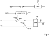
- FIG 4 illustrates a method implemented by the processing unit 38 to obtain the temperature T M of a scene element from two measured values V1 and V2 representative of temperature values of bolometric membranes of neighboring pixels 32 and 34 .
- the method includes by way of example the repetition of iterations.
- Each iteration takes as its starting point a pair of estimated values E E of emissivity and T E of temperature and determines a new pair of estimated values which will serve as a starting point for the following iteration.
- the estimated values E E and T E are respective initial values Ei and Ti which have been chosen beforehand, for example respectively a value Ei of any emissivity between 0 and 1 and a value Ti of temperature close to of ambient temperature.
- Each iteration includes a modeling step 62 (COMPUTE) which determines theoretical values V1 TH and V2 TH .
- the theoretical value V1 TH corresponds to the membrane temperature value that would be obtained if the scene element were at the estimated temperature T E , taking into account the absorption properties of the pixel 32 (schematized by the curve 52 of the picture 3 ), according to Planck's law weighted by the estimated emissivity E E . It is considered here that the emissivity E E is independent of the wavelength.
- the theoretical value V2 TH is determined in a similar way taking into account the absorption properties of the pixel 34 (schematized by the curve 54 of the picture 3 ).
- V1 TH and V2 TH can also take into account the absorption by elements between the scene element and the pixels, for example the atmosphere, or take into account transmission windows.
- a window is commonly disposed above the pixel array, or retina, to isolate the retina from the atmosphere.
- the transmission spectrum of such a window is known and can therefore easily be taken into account to determine the theoretical values.
- the measured values V1 and V2 are compared with the theoretical values V1 TH and V2 TH , which provides difference values V1-V1 TH and V2-V2 TH . These difference values are used in a step 66 (ERR) to determine an error value ⁇ 2.
- step 68 is a step of an algorithm for minimizing a value depending on two variables by successive evaluations of this value from successive estimates of the variables, such as a gradient method, conjugate gradient, simplex, etc. The process stops when the value of ⁇ 2 is minimum.
- the measured value T M of the temperature of the scene element is then the estimated value T E at the last iteration.
- the estimated value E E of the emissivity at the last iteration corresponds to a measured value E M of the emissivity of the scene element.
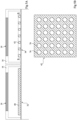
- FIG 5A is a sectional view of an alternative embodiment of two neighboring pixels 32 and 34, in which the dielectric layers 40 of the pixel 32 and 42 of the pixel 34 are made of the same material and have the same thicknesses.
- FIG 5B East a sectional top view of the layer 42 according to the plan BB of the figure 5A .
- Layer 42 is interrupted over its entire thickness by openings 70 arranged regularly.
- the openings 70 may have lateral dimensions smaller than the wavelengths of the infrared radiation received, for example smaller than one third of the smallest wavelength of the range of wavelengths of the radiation received.
- the pitch of the network pattern drawn by the openings is of the order of 1 to 3 ⁇ m.
- the openings shown have a circular shape, but any other suitable shape can be used.
- the neighboring openings can join together and the layer 42 is formed of a set of disjoint pads arranged regularly.
- Layer 42 thus has a network pattern of elements defined by the absence or presence of the material of layer 42, such as openings or studs, repeated in directions parallel to the plane of the layer.
- the refractive index n eff of the layer 42 can be roughly estimated by the product of the refractive index n s of the material of the layer 42 by the degree of filling f of the layer 42.
- the refractive index of layer 42 is thus lower than that of layer 40. Moreover, in the example shown in figure 5A , if, starting from the pattern drawn by the openings in the layer 42, this pattern is turned by a quarter turn, we fall back on the starting pattern, in other words this pattern has a symmetry of order four. Therefore the refractive index of the layer 42 does not depend on the polarization infrared radiation.
- the lattice pattern drawn by openings or studs can have a higher order symmetry, for example the symmetry of order six of a hexagonal lattice.
- the error value ⁇ 2 is calculated for a set of predefined pairs of estimated values T E of temperature and E E of emissivity scene element.
- the determined temperature and emissivity values correspond to the values of the predefined couple for which the value ⁇ 2 is minimum.
- the scene element temperature corresponding to the minimum of this error value can be chosen from a set of temperature values determined beforehand as a function of a set of values V1, V2 of membrane temperatures bolometrics. These previously determined values are then stored in the processing unit 38.
- a temperature value is determined in a particular way, it is possible to use any other method allowing the temperature of a scene element to be determined from temperature values of two bolometric membranes of two pixels of different types opposite the scene element.
- the absorption properties of the pixels can also be modeled by mathematical expressions making it possible to explicitly express the temperature of the scene element as a function of those of the membranes.
- the theoretical value V1 TH corresponds to the membrane temperature value that would be obtained if the stage element were at the previously known temperature, taking into account the absorption properties of the pixel 32, according to Planck's law weighted by a first value of emissivity estimated in the range of wavelengths of the pixel 32, the theoretical value V2 TH being determined similarly for a second estimated emissivity value.
- a reading circuit is provided to measure the temperature of bolometric membranes
- the reading circuit can be provided to measure any value representative of the temperature of the bolometric membranes, for example a resistance value.
- pixels of two different types are arranged in a checkerboard pattern
- these pixels can be arranged in any other way allowing each pixel of one type to be adjacent to a pixel of a Another type.
- an arrangement in alternating rows or columns of pixels of each type leads to the same advantages.
- the pixels of one type are more numerous, that is to say more densely arranged, than the pixels of another type, the proportions of the pixels being for example respectively 75% and 25%.
- any other suitable bolometric membrane can be used, for example a bolometric membrane having a different number of dielectric layers, or a membrane in which the measurement layer has been replaced by other temperature measurement structures, for example measurements of strains and/or stresses due to thermal expansion.
- the embodiments described include a particular type of reflector, it is possible to use any other reflector allowing the bolometric membrane to absorb, at more than 50% for the main part of the wavelengths concerned, the radiation emitted by stage elements.
- dielectric layers 42 having network patterns and solid dielectric layers 40 that is to say in each of which the material of the layer is present below the entirety of the membrane. bolometric.
- Various variants are possible. Provision can be made for each of the dielectric layers 40 and of the dielectric layers 42 to have a network pattern whose elements, for example openings or pads, are laterally repeated and have lateral dimensions smaller than the wavelength of the radiation received, for example less than a third of the smallest wavelength of the range of radiation concerned.
- the main thing then is that the patterns of the layers 40 and 42 are different.
- the range of wavelengths located between 7 and 14 ⁇ m is considered, it may be preferred to operate in another range of wavelengths, for example and typically in positioning this range, i.e. the transmission spectrum of a filter window, around the emission maximum according to the black body emission law at the average temperature of the scenes in question observe according to the particular intended application.
- this range i.e. the transmission spectrum of a filter window
- Those skilled in the art will know how to adapt the transmission spectrum of said window accordingly, as well as the pixels described in terms of dimensions, in particular according to the relationships described, in the space between membrane and reflector (distance D, thicknesses and /or indices of refraction of the dielectric layers) to produce the selective interferences of different wavelengths inscribed in said spectrum thus selected.
- the embodiments of sensors described are intended to capture infrared radiation located in a range which extends between 7 and 14 ⁇ m, other embodiments may be intended to capture infrared radiation located in a range extending between 8 and 12.5 ⁇ m.
- the sensor can be arranged under a transmission window intended to limit the radiation received by the sensor to the range between 8 and 12.5 ⁇ m.
- the thicknesses and the refractive indices of the dielectric layers 40 and 42 are then chosen so that destructive interference appears at the level of the membrane 14 for wavelengths close respectively to 8.5 ⁇ m and 12 ⁇ m.
- the dielectric layer 40 has a thickness substantially equal to 0.9 ⁇ m and a refractive index substantially equal to 3.5.
- the dielectric layer 42 has a thickness substantially equal to 0.9 ⁇ m and a refractive index substantially equal to 2.
- the other dimensions of the device are for example identical to the corresponding dimensions in the devices of the figures 2A and 2B .
- the sensor obtained has the advantage of excluding radiation with wavelengths greater than 12.5 ⁇ m, which is absorbed by the atmosphere, and the measurement of temperature or emissivity by the sensor is then independent of the quality the atmosphere and the distance between the sensor and the scene element. The temperature and emissivity measurement of such a sensor is then particularly precise.
- Embodiments described include pixels of only two different types absorbing more than 50% of the radiation located in two different ranges, these two ranges extending, in one example described, over more than 3 ⁇ m in width.
- Other different embodiments are possible comprising more than two types of pixel.
- each type of pixel is provided so that it absorbs more than 50% of the radiation in a range of wavelengths different from that of the other types of pixel.
- the extents of the wavelength ranges of the different types of pixels can be substantially identical. These ranges of wavelengths can cover the extent of the range of wavelengths of the radiation under consideration.
- the temperature of a scene element is then determined from the more than two bolometric membrane temperature values of the pixels of different types. This makes it possible to more precisely determine the temperature and the emissivity of the scene element, and to more precisely determine the temperature of scene elements whose emissivity varies according to the wavelength.
- pairs of pixels 32 and 34 of the type of those of the figure 2B are regularly dispersed in a set of pixels, or retina, comprising pixels 3 of the type of that of the figure 1B .
- the processing unit 38 produces a first thermal image from the pixels 3.
- the processing unit 38 superimposes on this first image a second image containing temperature and emissivity information determined from the pairs of pixels. Because the lateral dimensions of each pixel 3 are smaller than those of a pair of pixels, the first image can have a high resolution.
- the image obtained contains particularly precise temperature information and has a high resolution.
Landscapes
- Physics & Mathematics (AREA)
- General Physics & Mathematics (AREA)
- Spectroscopy & Molecular Physics (AREA)
- Engineering & Computer Science (AREA)
- Multimedia (AREA)
- Signal Processing (AREA)
- Photometry And Measurement Of Optical Pulse Characteristics (AREA)
- Transforming Light Signals Into Electric Signals (AREA)
- Radiation Pyrometers (AREA)
- Solid State Image Pick-Up Elements (AREA)
Claims (13)
- Ein Infrarot-Bildsensor, der Folgendes aufweist:- auf einem Träger (10) eine Vielzahl von ersten Pixeln (32) und eine Vielzahl von zweiten Pixeln (34), die dazu bestimmt sind, eine von einem Element einer Szene emittierte Infrarotstrahlung zu detektieren, wobei jedes Pixel eine bolometrische Membran (14) aufweist, die über einem den Träger bedeckenden Reflektor (12) aufgehängt ist, wobei der Reflektor jedes ersten Pixels mit einer ersten dielektrischen Schicht (40) bedeckt ist und der Reflektor jedes zweiten Pixels mit einer zweiten dielektrischen Schicht (42) bedeckt ist, die sich von der ersten dielektrischen Schicht durch ihre optischen Eigenschaften unterscheidet;- eine Leseschaltung (36) zum Auslesen erster Werte (V1, V2), die die Temperaturen der bolometrischen Membranen (14) von ersten und zweiten benachbarten Pixeln darstellen; und- eine Verarbeitungseinheit (38), die geeignet ist, die Emissivität des Szenenelements auf der Grundlage der ersten Werte (V1, V2) zu bestimmen, wobei die Verarbeitungseinheit konfiguriert ist zum Erzeugen geschätzter Temperatur-(Ti, TE) und Emissivitätswerte (Ei, EE), die einem Minimum eines Fehlerwerts entsprechen, der für Differenzen repräsentativ ist, wobei die Differenzen Folgendes aufweisen:eine erste Differenz zwischen dem ersten Wert (V1), der aus dem ersten Pixel ausgelesen wurde, und einem zweiten Wert (V1TH), der für die Temperatur repräsentativ ist, die die bolometrische Membran des ersten Pixels gemäß einem theoretischen Modell aufweisen würde, wenn die Temperatur und das Emissionsvermögen des Szenenelements die geschätzten Werte hätten; undeine zweite Differenz zwischen dem vom zweiten Pixel abgelesenen ersten Wert (V2) und einem weiteren zweiten Wert (V2TH), der für die Temperatur repräsentativ ist, die die bolometrische Membran des zweiten Pixels gemäß einem theoretischen Modell aufweisen würde, wenn die Temperatur und das Emissionsvermögen des Szenenelements den geschätzten Wert hätten.
- Sensor nach Anspruch 1, wobei der Fehlerwert eine gewichtete Summe der folgenden Form ist

- Der Sensor nach einem der Ansprüche 1 bis 2, wobei die Verarbeitungseinheit (38) konfiguriert ist, zum:a) Definieren eines Anfangspaars von geschätzten Temperatur- (Ti) und Emissivitätswerten (Ei);b) Berechnen der jeweiligen zweiten Werte (V1TH, V2TH) basierend auf den geschätzten Werten;c) Berechnen der Differenzen zwischen den jeweiligen ersten Werten (V1, V2) und den entsprechenden zweiten Werten;d) Erzeugen neuer geschätzter Werte für die Temperatur (TE) und die Emissivität (EE) auf der Grundlage dieser Differenzen; unde) Wiederholen der Schritte b), c) und d) auf der Grundlage der neuen geschätzten Werte, um die Differenzen zu verringern.
- Sensor nach einem der Ansprüche 1 bis 3, wobei der Unterschied der optischen Eigenschaft aus mindestens einem Merkmal der folgenden Liste resultiert:die erste (40) und die zweite (42) dielektrische Schicht haben unterschiedliche Dicken;die erste (40) und die zweite (42) dielektrische Schicht sind aus Materialien mit unterschiedlichen Brechungsindizes hergestellt;die erste Schicht (42) hat ein regelmäßiges Muster und die zweite Schicht (40) ist kontinuierlich; unddie erste (40) und die zweite (42) Schicht haben unterschiedliche regelmäßige Muster in der ersten Schicht und in der zweiten Schicht.
- Sensor nach einem der Ansprüche 1 bis 4 aufweisend eine Anordnung von Pixelpaaren aus einem der ersten Pixel (32) und einem der zweiten Pixel (34).
- Sensor nach einem der Ansprüche 1 bis 5, wobei die bolometrischen Membranen (14) aller Pixel strukturell identisch sind und die Reflektoren (12) aller Pixel strukturell identisch sind.
- Sensor nach einem der Ansprüche 1 bis 6, wobei die ersten (32) und zweiten (34) Pixel in einem Schachbrettmuster angeordnet sind.
- Sensor nach einem der Ansprüche 1 bis 7, der dazu bestimmt ist, Strahlungen mit Wellenlängen zu detektieren, die in einem Wellenlängenbereich liegen, wobei der Abstand in jedem Pixel zwischen der Membran und der dielektrischen Schicht gleich einem Viertel einer Wellenlänge ist, die in einem mittleren Teil des Bereichs liegt.
- Sensor nach Anspruch 8, wobei sich der Bereich zwischen 7 und 14 µm erstreckt und der Abstand im Bereich von 2 bis 3 µm liegt.
- Sensor nach Anspruch 8 oder 9, wobei für die erste dielektrische Schicht das Produkt aus der Dicke und dem Brechungsindex gleich einem Viertel einer ersten Wellenlänge ist und für die zweite dielektrische Schicht das Produkt aus der Dicke und dem Brechungsindex gleich einem Viertel einer zweiten Wellenlänge ist, wobei die erste und die zweite Wellenlänge innerhalb des Bereichs liegen und voneinander verschieden sind.
- Sensor nach einem der Ansprüche 8 bis 10, dadurch gekennzeichnet, dass die erste (40) und die zweite (42) dielektrische Schicht aus einem identischen Material bestehen und die gleiche Dicke aufweisen, wobei der Abstand zwischen der bolometrischen Membran (14) und der dielektrischen Schicht (40, 42) im ersten und im zweiten Pixel identisch ist, wobei jede zweite dielektrische Schicht ein regelmäßiges Muster aufweist, das aus Elementen gebildet ist, die in zur Schichtebene parallelen Richtungen Abmessungen aufweisen, die kleiner als ein Drittel der kleinsten Wellenlänge des genannten Bereichs sind.
- Sensor nach Anspruch 11, wobei die erste (40) und die zweite (42) dielektrische Schicht aus amorphem Silizium hergestellt sind.
- Sensor nach einem der Ansprüche 1 bis 12, der ferner eine Vielzahl von dritten Pixeln (3) aufweist, die dazu bestimmt sind, eine von der äußeren Szene emittierte Infrarotstrahlung zu detektieren, wobei jedes dritte Pixel eine bolometrische Membran aufweist, die über einem den Träger bedeckenden Reflektor aufgehängt ist, wobei der Reflektor nicht mit einer dielektrischen Schicht bedeckt ist.
Applications Claiming Priority (2)
| Application Number | Priority Date | Filing Date | Title |
|---|---|---|---|
| FR1662079A FR3059824B1 (fr) | 2016-12-07 | 2016-12-07 | Capteur d'image infrarouge |
| PCT/FR2017/053402 WO2018104653A1 (fr) | 2016-12-07 | 2017-12-05 | Capteur d'image infrarouge |
Publications (2)
| Publication Number | Publication Date |
|---|---|
| EP3551976A1 EP3551976A1 (de) | 2019-10-16 |
| EP3551976B1 true EP3551976B1 (de) | 2023-05-03 |
Family
ID=59649741
Family Applications (3)
| Application Number | Title | Priority Date | Filing Date |
|---|---|---|---|
| EP17816991.8A Withdrawn EP3551977A1 (de) | 2016-12-07 | 2017-12-05 | Infrarot-bildsensor |
| EP21206437.2A Pending EP3968382A1 (de) | 2016-12-07 | 2017-12-05 | Infrarot-bilderfassungssensor |
| EP17816990.0A Active EP3551976B1 (de) | 2016-12-07 | 2017-12-05 | Infrarotbildsensor |
Family Applications Before (2)
| Application Number | Title | Priority Date | Filing Date |
|---|---|---|---|
| EP17816991.8A Withdrawn EP3551977A1 (de) | 2016-12-07 | 2017-12-05 | Infrarot-bildsensor |
| EP21206437.2A Pending EP3968382A1 (de) | 2016-12-07 | 2017-12-05 | Infrarot-bilderfassungssensor |
Country Status (8)
| Country | Link |
|---|---|
| US (3) | US11015978B2 (de) |
| EP (3) | EP3551977A1 (de) |
| JP (2) | JP2020501149A (de) |
| KR (2) | KR20190094181A (de) |
| CN (3) | CN110073186B (de) |
| CA (2) | CA3045579A1 (de) |
| FR (1) | FR3059824B1 (de) |
| WO (2) | WO2018104653A1 (de) |
Families Citing this family (3)
| Publication number | Priority date | Publication date | Assignee | Title |
|---|---|---|---|---|
| FR3059824B1 (fr) | 2016-12-07 | 2019-06-21 | Ulis | Capteur d'image infrarouge |
| EP3938747A2 (de) | 2019-03-11 | 2022-01-19 | Flir Commercial Systems, Inc. | Mikrobolometersysteme und verfahren |
| US12342650B2 (en) | 2022-04-04 | 2025-06-24 | Omnivision Technologies, Inc. | Near infrared to far infrared polarization sensitive image sensor |
Family Cites Families (35)
| Publication number | Priority date | Publication date | Assignee | Title |
|---|---|---|---|---|
| JPS63305227A (ja) * | 1987-06-06 | 1988-12-13 | Minolta Camera Co Ltd | 放射温度計 |
| US4881823A (en) * | 1988-03-29 | 1989-11-21 | Purdue Research Foundation | Radiation thermometry |
| US5132922A (en) * | 1989-01-12 | 1992-07-21 | Massachusetts Institute Of Technology | Emissivity independent multiwavelength pyrometer |
| US5868496A (en) * | 1994-06-28 | 1999-02-09 | Massachusetts Institute Of Technology | Non-contact surface temperature, emissivity, and area estimation |
| JPH11326039A (ja) * | 1998-05-15 | 1999-11-26 | Nikon Corp | 熱型赤外線撮像装置および熱型赤外線受光素子 |
| US6292685B1 (en) * | 1998-09-11 | 2001-09-18 | Exergen Corporation | Temporal artery temperature detector |
| US6715548B2 (en) * | 2000-04-24 | 2004-04-06 | Shell Oil Company | In situ thermal processing of a hydrocarbon containing formation to produce nitrogen containing formation fluids |
| JP2003294523A (ja) * | 2002-04-03 | 2003-10-15 | Mitsubishi Electric Corp | 赤外線検出器およびその製造方法、並びに赤外線固体撮像装置 |
| WO2004059247A1 (en) * | 2002-12-20 | 2004-07-15 | International Business Machines Corporation | Assessment and optimization for metrology instrument |
| EP1590692A2 (de) | 2003-01-30 | 2005-11-02 | DEL GRANDE, Nancy K. | Thermisches abbildungsverfahren zur erkennung von unteroberflächenobjekten |
| US7887234B2 (en) * | 2006-10-20 | 2011-02-15 | Siemens Corporation | Maximum blade surface temperature estimation for advanced stationary gas turbines in near-infrared (with reflection) |
| JP5251310B2 (ja) * | 2008-07-08 | 2013-07-31 | 日本電気株式会社 | 2波長熱型赤外線アレイセンサ |
| CN102265125B (zh) | 2008-10-23 | 2015-09-30 | Kaz欧洲有限公司 | 具有杂散辐射屏蔽的非接触式医用温度计 |
| US8129682B2 (en) * | 2009-02-26 | 2012-03-06 | Texas Instruments Incorporated | On-chip calibration system and method for infrared sensor |
| US8457922B2 (en) | 2009-03-27 | 2013-06-04 | Fluke Corporation | System and method for determining accuracy of an infrared thermometer measurement |
| KR101736418B1 (ko) * | 2010-10-14 | 2017-05-16 | 세미-컨덕터 디바이스-언 엘벗 시스템즈-라파엘 파트너쉽 | 적외선 검출 시스템용 듀어 조립체 |
| FR2966925B1 (fr) * | 2010-11-03 | 2012-11-02 | Commissariat Energie Atomique | Detecteur infrarouge a base de micro-planches bolometriques suspendues |
| JP5781351B2 (ja) | 2011-03-30 | 2015-09-24 | 日本アビオニクス株式会社 | 撮像装置、その画素出力レベル補正方法、赤外線カメラシステム及び交換可能なレンズシステム |
| FR2976072B1 (fr) * | 2011-05-31 | 2014-09-12 | Commissariat Energie Atomique | Detecteur spectroscopique et detecteur de gaz incluant au moins un tel detecteur |
| FR2977937B1 (fr) * | 2011-07-15 | 2013-08-16 | Centre Nat Rech Scient | Detecteur bolometrique a performances ameliorees |
| FR2983953B1 (fr) * | 2011-12-09 | 2014-01-03 | Commissariat Energie Atomique | Detecteur bolometrique d'un rayonnement electromagnetique dans le domaine du terahertz et dispositif de detection matriciel comportant de tels detecteurs |
| US9274005B2 (en) * | 2012-08-23 | 2016-03-01 | Robert Bosch Gmbh | Device and method for increasing infrared absorption in MEMS bolometers |
| US9733404B2 (en) * | 2012-09-06 | 2017-08-15 | Vaisala Oyj | Layered structure for an infrared emitter, infrared emitter device and detector |
| US20140140370A1 (en) * | 2012-11-19 | 2014-05-22 | Kaz Usa, Inc. | Medical thermometer having an improved optics system |
| CN205157051U (zh) * | 2012-11-26 | 2016-04-13 | 菲力尔系统公司 | 红外传感器组件 |
| CN103106332B (zh) * | 2012-12-13 | 2015-09-23 | 华中科技大学 | 一种测量不确定度的分析方法 |
| FR3017456B1 (fr) * | 2014-02-12 | 2017-06-23 | Commissariat Energie Atomique | Detecteur bolometrique a structure mim incluant un element thermometre |
| CN105527026B (zh) * | 2014-09-29 | 2019-04-12 | 华中科技大学 | 一种像素单元及其构成的红外成像探测器 |
| EP3035015B1 (de) * | 2014-12-15 | 2017-04-12 | Melexis Technologies NV | Ir-sensor zur ir-messung auf basis von leistungsregelung |
| US9846083B2 (en) | 2014-12-17 | 2017-12-19 | Maxim Integrated Products, Inc. | Ambient temperature measurement sensor |
| US9404804B1 (en) * | 2015-04-02 | 2016-08-02 | Palo Alto Research Center Incorporated | Thermal sensor with infrared absorption membrane including metamaterial structure |
| FR3042272B1 (fr) * | 2015-10-09 | 2017-12-15 | Commissariat Energie Atomique | Bolometre a forte sensibilite spectrale. |
| CN106006541B (zh) * | 2016-07-19 | 2017-07-18 | 中国科学院重庆绿色智能技术研究院 | 一种多孔碳纳米薄膜及其微测辐射热计 |
| FR3059824B1 (fr) | 2016-12-07 | 2019-06-21 | Ulis | Capteur d'image infrarouge |
| EP3486623B1 (de) * | 2017-11-17 | 2019-10-30 | Melexis Technologies NV | Infrarotdetektor mit geringer drift |
-
2016
- 2016-12-07 FR FR1662079A patent/FR3059824B1/fr active Active
-
2017
- 2017-12-05 US US16/466,723 patent/US11015978B2/en active Active
- 2017-12-05 CN CN201780075805.4A patent/CN110073186B/zh active Active
- 2017-12-05 JP JP2019530086A patent/JP2020501149A/ja active Pending
- 2017-12-05 KR KR1020197018258A patent/KR20190094181A/ko not_active Ceased
- 2017-12-05 EP EP17816991.8A patent/EP3551977A1/de not_active Withdrawn
- 2017-12-05 CN CN201780076168.2A patent/CN110050176B/zh active Active
- 2017-12-05 WO PCT/FR2017/053402 patent/WO2018104653A1/fr not_active Ceased
- 2017-12-05 JP JP2019530054A patent/JP2020513553A/ja active Pending
- 2017-12-05 CA CA3045579A patent/CA3045579A1/fr not_active Abandoned
- 2017-12-05 EP EP21206437.2A patent/EP3968382A1/de active Pending
- 2017-12-05 WO PCT/FR2017/053403 patent/WO2018104654A1/fr not_active Ceased
- 2017-12-05 KR KR1020197019147A patent/KR20190094194A/ko not_active Ceased
- 2017-12-05 EP EP17816990.0A patent/EP3551976B1/de active Active
- 2017-12-05 CA CA3045580A patent/CA3045580A1/fr not_active Abandoned
- 2017-12-05 CN CN202210137999.9A patent/CN114544001A/zh active Pending
- 2017-12-05 US US16/466,773 patent/US11060919B2/en active Active
-
2021
- 2021-05-20 US US17/325,827 patent/US11761820B2/en active Active
Also Published As
| Publication number | Publication date |
|---|---|
| US20200064200A1 (en) | 2020-02-27 |
| KR20190094194A (ko) | 2019-08-12 |
| JP2020501149A (ja) | 2020-01-16 |
| KR20190094181A (ko) | 2019-08-12 |
| EP3968382A1 (de) | 2022-03-16 |
| EP3551977A1 (de) | 2019-10-16 |
| CN110073186A (zh) | 2019-07-30 |
| CN110073186B (zh) | 2021-10-29 |
| JP2020513553A (ja) | 2020-05-14 |
| EP3551976A1 (de) | 2019-10-16 |
| CN114544001A (zh) | 2022-05-27 |
| US11015978B2 (en) | 2021-05-25 |
| WO2018104653A1 (fr) | 2018-06-14 |
| CN110050176B (zh) | 2023-01-13 |
| CA3045579A1 (fr) | 2018-06-14 |
| US11060919B2 (en) | 2021-07-13 |
| FR3059824A1 (fr) | 2018-06-08 |
| US20210270676A1 (en) | 2021-09-02 |
| CN110050176A (zh) | 2019-07-23 |
| WO2018104654A1 (fr) | 2018-06-14 |
| FR3059824B1 (fr) | 2019-06-21 |
| CA3045580A1 (fr) | 2018-06-14 |
| US11761820B2 (en) | 2023-09-19 |
| US20200083277A1 (en) | 2020-03-12 |
Similar Documents
| Publication | Publication Date | Title |
|---|---|---|
| EP3607585B1 (de) | Vorrichtung und verfahren zur multispektralen bildgebung im infrarotbereich | |
| FR2977937A1 (fr) | Detecteur bolometrique a performances ameliorees | |
| FR3059824B1 (fr) | Capteur d'image infrarouge | |
| FR2965922A1 (fr) | Dispositif et methode d'identification de la conductivite et/ou de la capacite thermique d'une paroi | |
| CA2637223A1 (fr) | Detecteur de rayonnement electromagnetique et procede de fabrication d'un tel detecteur | |
| WO2018210647A1 (fr) | Procédé de traitement d'une image optique acquise en présence d'aérosols et/ou de nuages dans l'atmosphère | |
| EP1787085A1 (de) | Verfahren zum messen dreidimensionaler objekte durch rückbeleuchtete schattenprojektion mit einer einzigen ansicht unter verwendung optischer gesetze der lichtausbreitung | |
| WO2018002558A1 (fr) | Spectro-imageur multivoie a transformee de fourier | |
| FR2842301A1 (fr) | Procede et dispositif de mesure de la distribution de temperature | |
| WO2003044499A2 (fr) | Procede de detection optique de gaz a distance | |
| EP2520916A1 (de) | Multispektrales Scanteleskop mit Wellenfrontanalysemitteln. | |
| FR2775084A1 (fr) | Telemetre passif | |
| FR2993972A1 (fr) | Dispositif de determination d'un ensemble de donnees spatiales d'epaisseur d'une couche mince a la surface d'un substrat, par mesure d'emission infra-rouge | |
| EP2708862B1 (de) | Optischer Wellenfrontanalysator | |
| Zucco et al. | A novel hyperspectral camera concept for SWIR-MWIR applications | |
| FR3066592A1 (fr) | Dispositif adapte a etre embarque a bord d'un vehicule pour de la cartographie thermique | |
| JPH0843211A (ja) | 温度ならびに放射率測定方法 | |
| EP3835756A1 (de) | Vorrichtung und verfahren zur partikeldetektion und verfahren zur herstellung | |
| Tian | SNR simulation with TDI set for lake water color monitoring oriented satellite RS system |
Legal Events
| Date | Code | Title | Description |
|---|---|---|---|
| STAA | Information on the status of an ep patent application or granted ep patent |
Free format text: STATUS: UNKNOWN |
|
| STAA | Information on the status of an ep patent application or granted ep patent |
Free format text: STATUS: THE INTERNATIONAL PUBLICATION HAS BEEN MADE |
|
| PUAI | Public reference made under article 153(3) epc to a published international application that has entered the european phase |
Free format text: ORIGINAL CODE: 0009012 |
|
| STAA | Information on the status of an ep patent application or granted ep patent |
Free format text: STATUS: REQUEST FOR EXAMINATION WAS MADE |
|
| 17P | Request for examination filed |
Effective date: 20190625 |
|
| AK | Designated contracting states |
Kind code of ref document: A1 Designated state(s): AL AT BE BG CH CY CZ DE DK EE ES FI FR GB GR HR HU IE IS IT LI LT LU LV MC MK MT NL NO PL PT RO RS SE SI SK SM TR |
|
| AX | Request for extension of the european patent |
Extension state: BA ME |
|
| DAV | Request for validation of the european patent (deleted) | ||
| DAX | Request for extension of the european patent (deleted) | ||
| STAA | Information on the status of an ep patent application or granted ep patent |
Free format text: STATUS: EXAMINATION IS IN PROGRESS |
|
| 17Q | First examination report despatched |
Effective date: 20210224 |
|
| RAP1 | Party data changed (applicant data changed or rights of an application transferred) |
Owner name: LYNRED |
|
| GRAP | Despatch of communication of intention to grant a patent |
Free format text: ORIGINAL CODE: EPIDOSNIGR1 |
|
| STAA | Information on the status of an ep patent application or granted ep patent |
Free format text: STATUS: GRANT OF PATENT IS INTENDED |
|
| RIC1 | Information provided on ipc code assigned before grant |
Ipc: H01L 27/146 20060101ALI20221115BHEP Ipc: G01J 5/08 20060101ALI20221115BHEP Ipc: G01J 5/02 20060101ALI20221115BHEP Ipc: G01J 5/20 20060101AFI20221115BHEP |
|
| INTG | Intention to grant announced |
Effective date: 20221201 |
|
| GRAS | Grant fee paid |
Free format text: ORIGINAL CODE: EPIDOSNIGR3 |
|
| GRAA | (expected) grant |
Free format text: ORIGINAL CODE: 0009210 |
|
| STAA | Information on the status of an ep patent application or granted ep patent |
Free format text: STATUS: THE PATENT HAS BEEN GRANTED |
|
| AK | Designated contracting states |
Kind code of ref document: B1 Designated state(s): AL AT BE BG CH CY CZ DE DK EE ES FI FR GB GR HR HU IE IS IT LI LT LU LV MC MK MT NL NO PL PT RO RS SE SI SK SM TR |
|
| REG | Reference to a national code |
Ref country code: GB Ref legal event code: FG4D Free format text: NOT ENGLISH |
|
| REG | Reference to a national code |
Ref country code: AT Ref legal event code: REF Ref document number: 1564989 Country of ref document: AT Kind code of ref document: T Effective date: 20230515 Ref country code: CH Ref legal event code: EP |
|
| REG | Reference to a national code |
Ref country code: DE Ref legal event code: R096 Ref document number: 602017068375 Country of ref document: DE |
|
| REG | Reference to a national code |
Ref country code: IE Ref legal event code: FG4D Free format text: LANGUAGE OF EP DOCUMENT: FRENCH |
|
| REG | Reference to a national code |
Ref country code: LT Ref legal event code: MG9D |
|
| REG | Reference to a national code |
Ref country code: NL Ref legal event code: MP Effective date: 20230503 |
|
| REG | Reference to a national code |
Ref country code: AT Ref legal event code: MK05 Ref document number: 1564989 Country of ref document: AT Kind code of ref document: T Effective date: 20230503 |
|
| PG25 | Lapsed in a contracting state [announced via postgrant information from national office to epo] |
Ref country code: SE Free format text: LAPSE BECAUSE OF FAILURE TO SUBMIT A TRANSLATION OF THE DESCRIPTION OR TO PAY THE FEE WITHIN THE PRESCRIBED TIME-LIMIT Effective date: 20230503 Ref country code: PT Free format text: LAPSE BECAUSE OF FAILURE TO SUBMIT A TRANSLATION OF THE DESCRIPTION OR TO PAY THE FEE WITHIN THE PRESCRIBED TIME-LIMIT Effective date: 20230904 Ref country code: NO Free format text: LAPSE BECAUSE OF FAILURE TO SUBMIT A TRANSLATION OF THE DESCRIPTION OR TO PAY THE FEE WITHIN THE PRESCRIBED TIME-LIMIT Effective date: 20230803 Ref country code: NL Free format text: LAPSE BECAUSE OF FAILURE TO SUBMIT A TRANSLATION OF THE DESCRIPTION OR TO PAY THE FEE WITHIN THE PRESCRIBED TIME-LIMIT Effective date: 20230503 Ref country code: ES Free format text: LAPSE BECAUSE OF FAILURE TO SUBMIT A TRANSLATION OF THE DESCRIPTION OR TO PAY THE FEE WITHIN THE PRESCRIBED TIME-LIMIT Effective date: 20230503 Ref country code: AT Free format text: LAPSE BECAUSE OF FAILURE TO SUBMIT A TRANSLATION OF THE DESCRIPTION OR TO PAY THE FEE WITHIN THE PRESCRIBED TIME-LIMIT Effective date: 20230503 |
|
| PG25 | Lapsed in a contracting state [announced via postgrant information from national office to epo] |
Ref country code: RS Free format text: LAPSE BECAUSE OF FAILURE TO SUBMIT A TRANSLATION OF THE DESCRIPTION OR TO PAY THE FEE WITHIN THE PRESCRIBED TIME-LIMIT Effective date: 20230503 Ref country code: PL Free format text: LAPSE BECAUSE OF FAILURE TO SUBMIT A TRANSLATION OF THE DESCRIPTION OR TO PAY THE FEE WITHIN THE PRESCRIBED TIME-LIMIT Effective date: 20230503 Ref country code: LV Free format text: LAPSE BECAUSE OF FAILURE TO SUBMIT A TRANSLATION OF THE DESCRIPTION OR TO PAY THE FEE WITHIN THE PRESCRIBED TIME-LIMIT Effective date: 20230503 Ref country code: LT Free format text: LAPSE BECAUSE OF FAILURE TO SUBMIT A TRANSLATION OF THE DESCRIPTION OR TO PAY THE FEE WITHIN THE PRESCRIBED TIME-LIMIT Effective date: 20230503 Ref country code: IS Free format text: LAPSE BECAUSE OF FAILURE TO SUBMIT A TRANSLATION OF THE DESCRIPTION OR TO PAY THE FEE WITHIN THE PRESCRIBED TIME-LIMIT Effective date: 20230903 Ref country code: HR Free format text: LAPSE BECAUSE OF FAILURE TO SUBMIT A TRANSLATION OF THE DESCRIPTION OR TO PAY THE FEE WITHIN THE PRESCRIBED TIME-LIMIT Effective date: 20230503 Ref country code: GR Free format text: LAPSE BECAUSE OF FAILURE TO SUBMIT A TRANSLATION OF THE DESCRIPTION OR TO PAY THE FEE WITHIN THE PRESCRIBED TIME-LIMIT Effective date: 20230804 |
|
| PG25 | Lapsed in a contracting state [announced via postgrant information from national office to epo] |
Ref country code: FI Free format text: LAPSE BECAUSE OF FAILURE TO SUBMIT A TRANSLATION OF THE DESCRIPTION OR TO PAY THE FEE WITHIN THE PRESCRIBED TIME-LIMIT Effective date: 20230503 |
|
| PG25 | Lapsed in a contracting state [announced via postgrant information from national office to epo] |
Ref country code: SK Free format text: LAPSE BECAUSE OF FAILURE TO SUBMIT A TRANSLATION OF THE DESCRIPTION OR TO PAY THE FEE WITHIN THE PRESCRIBED TIME-LIMIT Effective date: 20230503 |
|
| PG25 | Lapsed in a contracting state [announced via postgrant information from national office to epo] |
Ref country code: SM Free format text: LAPSE BECAUSE OF FAILURE TO SUBMIT A TRANSLATION OF THE DESCRIPTION OR TO PAY THE FEE WITHIN THE PRESCRIBED TIME-LIMIT Effective date: 20230503 Ref country code: SK Free format text: LAPSE BECAUSE OF FAILURE TO SUBMIT A TRANSLATION OF THE DESCRIPTION OR TO PAY THE FEE WITHIN THE PRESCRIBED TIME-LIMIT Effective date: 20230503 Ref country code: RO Free format text: LAPSE BECAUSE OF FAILURE TO SUBMIT A TRANSLATION OF THE DESCRIPTION OR TO PAY THE FEE WITHIN THE PRESCRIBED TIME-LIMIT Effective date: 20230503 Ref country code: EE Free format text: LAPSE BECAUSE OF FAILURE TO SUBMIT A TRANSLATION OF THE DESCRIPTION OR TO PAY THE FEE WITHIN THE PRESCRIBED TIME-LIMIT Effective date: 20230503 Ref country code: DK Free format text: LAPSE BECAUSE OF FAILURE TO SUBMIT A TRANSLATION OF THE DESCRIPTION OR TO PAY THE FEE WITHIN THE PRESCRIBED TIME-LIMIT Effective date: 20230503 Ref country code: CZ Free format text: LAPSE BECAUSE OF FAILURE TO SUBMIT A TRANSLATION OF THE DESCRIPTION OR TO PAY THE FEE WITHIN THE PRESCRIBED TIME-LIMIT Effective date: 20230503 |
|
| REG | Reference to a national code |
Ref country code: DE Ref legal event code: R097 Ref document number: 602017068375 Country of ref document: DE |
|
| PLBE | No opposition filed within time limit |
Free format text: ORIGINAL CODE: 0009261 |
|
| STAA | Information on the status of an ep patent application or granted ep patent |
Free format text: STATUS: NO OPPOSITION FILED WITHIN TIME LIMIT |
|
| 26N | No opposition filed |
Effective date: 20240206 |
|
| PG25 | Lapsed in a contracting state [announced via postgrant information from national office to epo] |
Ref country code: SI Free format text: LAPSE BECAUSE OF FAILURE TO SUBMIT A TRANSLATION OF THE DESCRIPTION OR TO PAY THE FEE WITHIN THE PRESCRIBED TIME-LIMIT Effective date: 20230503 |
|
| PG25 | Lapsed in a contracting state [announced via postgrant information from national office to epo] |
Ref country code: SI Free format text: LAPSE BECAUSE OF FAILURE TO SUBMIT A TRANSLATION OF THE DESCRIPTION OR TO PAY THE FEE WITHIN THE PRESCRIBED TIME-LIMIT Effective date: 20230503 Ref country code: IT Free format text: LAPSE BECAUSE OF FAILURE TO SUBMIT A TRANSLATION OF THE DESCRIPTION OR TO PAY THE FEE WITHIN THE PRESCRIBED TIME-LIMIT Effective date: 20230503 |
|
| REG | Reference to a national code |
Ref country code: CH Ref legal event code: PL |
|
| PG25 | Lapsed in a contracting state [announced via postgrant information from national office to epo] |
Ref country code: LU Free format text: LAPSE BECAUSE OF NON-PAYMENT OF DUE FEES Effective date: 20231205 |
|
| PG25 | Lapsed in a contracting state [announced via postgrant information from national office to epo] |
Ref country code: MC Free format text: LAPSE BECAUSE OF FAILURE TO SUBMIT A TRANSLATION OF THE DESCRIPTION OR TO PAY THE FEE WITHIN THE PRESCRIBED TIME-LIMIT Effective date: 20230503 |
|
| REG | Reference to a national code |
Ref country code: BE Ref legal event code: MM Effective date: 20231231 |
|
| PG25 | Lapsed in a contracting state [announced via postgrant information from national office to epo] |
Ref country code: MC Free format text: LAPSE BECAUSE OF FAILURE TO SUBMIT A TRANSLATION OF THE DESCRIPTION OR TO PAY THE FEE WITHIN THE PRESCRIBED TIME-LIMIT Effective date: 20230503 Ref country code: LU Free format text: LAPSE BECAUSE OF NON-PAYMENT OF DUE FEES Effective date: 20231205 |
|
| REG | Reference to a national code |
Ref country code: IE Ref legal event code: MM4A |
|
| PG25 | Lapsed in a contracting state [announced via postgrant information from national office to epo] |
Ref country code: IE Free format text: LAPSE BECAUSE OF NON-PAYMENT OF DUE FEES Effective date: 20231205 |
|
| PG25 | Lapsed in a contracting state [announced via postgrant information from national office to epo] |
Ref country code: BE Free format text: LAPSE BECAUSE OF NON-PAYMENT OF DUE FEES Effective date: 20231231 |
|
| PG25 | Lapsed in a contracting state [announced via postgrant information from national office to epo] |
Ref country code: CH Free format text: LAPSE BECAUSE OF NON-PAYMENT OF DUE FEES Effective date: 20231231 |
|
| PG25 | Lapsed in a contracting state [announced via postgrant information from national office to epo] |
Ref country code: IE Free format text: LAPSE BECAUSE OF NON-PAYMENT OF DUE FEES Effective date: 20231205 Ref country code: CH Free format text: LAPSE BECAUSE OF NON-PAYMENT OF DUE FEES Effective date: 20231231 Ref country code: BE Free format text: LAPSE BECAUSE OF NON-PAYMENT OF DUE FEES Effective date: 20231231 |
|
| PG25 | Lapsed in a contracting state [announced via postgrant information from national office to epo] |
Ref country code: BG Free format text: LAPSE BECAUSE OF FAILURE TO SUBMIT A TRANSLATION OF THE DESCRIPTION OR TO PAY THE FEE WITHIN THE PRESCRIBED TIME-LIMIT Effective date: 20230503 |
|
| PG25 | Lapsed in a contracting state [announced via postgrant information from national office to epo] |
Ref country code: BG Free format text: LAPSE BECAUSE OF FAILURE TO SUBMIT A TRANSLATION OF THE DESCRIPTION OR TO PAY THE FEE WITHIN THE PRESCRIBED TIME-LIMIT Effective date: 20230503 |
|
| PGFP | Annual fee paid to national office [announced via postgrant information from national office to epo] |
Ref country code: DE Payment date: 20241216 Year of fee payment: 8 |
|
| PGFP | Annual fee paid to national office [announced via postgrant information from national office to epo] |
Ref country code: GB Payment date: 20241218 Year of fee payment: 8 |
|
| PGFP | Annual fee paid to national office [announced via postgrant information from national office to epo] |
Ref country code: FR Payment date: 20241218 Year of fee payment: 8 |
|
| PG25 | Lapsed in a contracting state [announced via postgrant information from national office to epo] |
Ref country code: CY Free format text: LAPSE BECAUSE OF FAILURE TO SUBMIT A TRANSLATION OF THE DESCRIPTION OR TO PAY THE FEE WITHIN THE PRESCRIBED TIME-LIMIT; INVALID AB INITIO Effective date: 20171205 |
|
| PG25 | Lapsed in a contracting state [announced via postgrant information from national office to epo] |
Ref country code: HU Free format text: LAPSE BECAUSE OF FAILURE TO SUBMIT A TRANSLATION OF THE DESCRIPTION OR TO PAY THE FEE WITHIN THE PRESCRIBED TIME-LIMIT; INVALID AB INITIO Effective date: 20171205 |
|
| PG25 | Lapsed in a contracting state [announced via postgrant information from national office to epo] |
Ref country code: TR Free format text: LAPSE BECAUSE OF FAILURE TO SUBMIT A TRANSLATION OF THE DESCRIPTION OR TO PAY THE FEE WITHIN THE PRESCRIBED TIME-LIMIT Effective date: 20230503 |