EP3550439B1 - Informationsverarbeitungssystem, integrierte halbleiterschaltung und informationsverarbeitungsverfahren - Google Patents
Informationsverarbeitungssystem, integrierte halbleiterschaltung und informationsverarbeitungsverfahren Download PDFInfo
- Publication number
- EP3550439B1 EP3550439B1 EP17877100.2A EP17877100A EP3550439B1 EP 3550439 B1 EP3550439 B1 EP 3550439B1 EP 17877100 A EP17877100 A EP 17877100A EP 3550439 B1 EP3550439 B1 EP 3550439B1
- Authority
- EP
- European Patent Office
- Prior art keywords
- address
- semiconductor integrated
- integrated circuit
- memory
- circuit
- Prior art date
- Legal status (The legal status is an assumption and is not a legal conclusion. Google has not performed a legal analysis and makes no representation as to the accuracy of the status listed.)
- Active
Links
Images




Classifications
-
- G—PHYSICS
- G06—COMPUTING OR CALCULATING; COUNTING
- G06F—ELECTRIC DIGITAL DATA PROCESSING
- G06F13/00—Interconnection of, or transfer of information or other signals between, memories, input/output devices or central processing units
- G06F13/38—Information transfer, e.g. on bus
- G06F13/40—Bus structure
- G06F13/4004—Coupling between buses
- G06F13/4022—Coupling between buses using switching circuits, e.g. switching matrix, connection or expansion network
-
- G—PHYSICS
- G06—COMPUTING OR CALCULATING; COUNTING
- G06F—ELECTRIC DIGITAL DATA PROCESSING
- G06F13/00—Interconnection of, or transfer of information or other signals between, memories, input/output devices or central processing units
- G06F13/14—Handling requests for interconnection or transfer
- G06F13/36—Handling requests for interconnection or transfer for access to common bus or bus system
-
- G—PHYSICS
- G06—COMPUTING OR CALCULATING; COUNTING
- G06F—ELECTRIC DIGITAL DATA PROCESSING
- G06F13/00—Interconnection of, or transfer of information or other signals between, memories, input/output devices or central processing units
- G06F13/38—Information transfer, e.g. on bus
-
- G—PHYSICS
- G06—COMPUTING OR CALCULATING; COUNTING
- G06F—ELECTRIC DIGITAL DATA PROCESSING
- G06F13/00—Interconnection of, or transfer of information or other signals between, memories, input/output devices or central processing units
- G06F13/38—Information transfer, e.g. on bus
- G06F13/42—Bus transfer protocol, e.g. handshake; Synchronisation
-
- Y—GENERAL TAGGING OF NEW TECHNOLOGICAL DEVELOPMENTS; GENERAL TAGGING OF CROSS-SECTIONAL TECHNOLOGIES SPANNING OVER SEVERAL SECTIONS OF THE IPC; TECHNICAL SUBJECTS COVERED BY FORMER USPC CROSS-REFERENCE ART COLLECTIONS [XRACs] AND DIGESTS
- Y02—TECHNOLOGIES OR APPLICATIONS FOR MITIGATION OR ADAPTATION AGAINST CLIMATE CHANGE
- Y02D—CLIMATE CHANGE MITIGATION TECHNOLOGIES IN INFORMATION AND COMMUNICATION TECHNOLOGIES [ICT], I.E. INFORMATION AND COMMUNICATION TECHNOLOGIES AIMING AT THE REDUCTION OF THEIR OWN ENERGY USE
- Y02D10/00—Energy efficient computing, e.g. low power processors, power management or thermal management
Definitions
- the embodiments discussed herein are related to an information processing system, a semiconductor integrated circuit, and an information processing method.
- SoCs Systems on Chip
- a CPU Central Processing Unit
- CPU Central Processing Unit
- PCIe Peripheral Component Interconnect express
- the cluster As a tightly-coupled cluster, the individual CPUs perform cooperative processing using a shared memory and/or intra-process communication.
- the network that connects the plurality of CPUs it would be conceivable to use an Ethernet that is capable of high-speed communication at a comparatively low cost.
- protocol overheads such as a transmitter having to wait for reception of a response signal from the destination before performing the next transmission, which limits how fast a tightly-coupled cluster can operate.
- FIG. 1 depicts one example of an information processing system according to a first embodiment.
- An information processing system 10 includes semiconductor integrated circuits 11 and 12, a switch 13, and memories 14 and 15.
- the semiconductor integrated circuits 11 and 12 and the switch 13 are all single-chip SoCs. Although two semiconductor integrated circuits 11 and 12 and one switch 13 are illustrated in FIG. 1 to simplify the description, the information processing system 10 is not limited to these numbers. An example of an information processing system including three or more semiconductor integrated circuits and two or more switches will be described later.
- the semiconductor integrated circuit 11 includes a control circuit 11a, an interrupt control circuit 11b, an address converting circuit 11c, a PCIe interface 11d, and a system bus 11e.
- the memory 14 is connected to the semiconductor integrated circuit 11.
- the control circuit 11a controls the various components of the semiconductor integrated circuit 11 via the system bus 11e to execute a variety of application processing.
- the control circuit 11a is a microcontroller, a CPU, or a CPU including a plurality of CPU cores.
- the interrupt control circuit 11b notifies the control circuit 11a of the occurrence of an interrupt based on an interrupt setting value set in a storage circuit (referred to hereinafter as an "interrupt setting register"), not illustrated.
- the address converting circuit 11c converts addresses based on memory map information 11m and 12m, in which addresses in the memories 14 and 15 that are used by the plurality of semiconductor integrated circuits 11 and 12 and the like are defined.
- the PCIe interface 11d is one example of a bus interface capable of transmitting continuously without waiting for a response from the transmission destination, and transmits and receives information to and from the switch 13 via a PCIe bus.
- the semiconductor integrated circuit 12 includes a control circuit 12a, an interrupt control circuit 12b, an address converting circuit 12c, a PCIe interface 12d, and a system bus 12e.
- the switch 13 includes PCIe interfaces 13a and 13b, and a system bus 13c that connects the PCIe interfaces 13a and 13b.
- the PCIe interface 13a transmits and receives information to and from the PCIe interface 11d of the semiconductor integrated circuit 11.
- the PCIe interface 13b transmits and receives information to and from the PCIe interface 12d of the semiconductor integrated circuit 12.
- the PCIe interfaces 11d, 12d, 13a, and 13b are used in the information processing system 10 like that depicted in FIG. 1 , the PCIe interfaces 11d and 12d are set so that the semiconductor integrated circuits 11 and 12 are end points.
- the PCIe interfaces 13a and 13b are set so that the switch 13 is a root complex.
- USB Universal Serial Bus
- the memories 14 and 15 are memories that are connected to the semiconductor integrated circuits 11 and 12, respectively, and store programs to be executed by the control circuits 11a and 12a and various data (which includes reception data and the like).
- the memories 14 and 15 may be volatile semiconductor memories, such as DRAM (Dynamic Random Access Memory) or may be volatile storage, such as flash memory. Note that the memories 14 and 15 may be included in the semiconductor integrated circuits 11 and 12.
- the memories 14 and 15 may each be composed of a plurality of memories.
- the semiconductor integrated circuit 11 may be referred to as "SOC1" and the semiconductor integrated circuit 12 as "SOC2".
- control circuit 11a When transmitting data to the semiconductor integrated circuit 12, the control circuit 11a designates an address based on the memory map information 11m of SOC1 like that depicted in FIG. 1 .
- An address of a memory space of the memory 14 of the same SOC (that is, SOC1) and an address of a memory space of the memory 15 of the other SOC (that is, SOC2) are defined in the memory map information 11m.
- An address of an interrupt setting register space of the same SOC and an address of an interrupt setting register space of the other SOC are also defined in the memory map information 11m.
- interrupt setting registers (not illustrated) are provided inside the interrupt control circuits 11b and 12b.
- the address of the memory space of the memory 15 of the same SOC (that is, SOC2) and the address of the memory space of the memory 14 of the other SOC (that is, SOC1) are defined in the same way as in the memory map information 11m.
- the address of the interrupt setting register space of the same SOC and the address of the interrupt setting register space of the other SOC are also defined in the memory map information 12m.
- control circuit 11a When transmitting data to the semiconductor integrated circuit 12, the control circuit 11a designates an address defined in the memory map information 11m of the memory 15 into which the data (transmission data) is to be written.
- FIG. 1 depicts an example where the control circuit 11a has designated an address a1 of the other SOC memory space defined in the memory map information 11m.
- the address converting circuit 11c uses a conversion table or the like, not depicted, to convert the address a1 to an address a3 of a memory space of SOC2 that is defined in the memory map information 12m of SOC2.
- the PCIe interface 11d outputs (that is, transmits) the converted address a3 and the transmission data.
- the address a3 and the transmission data are transferred to the semiconductor integrated circuit 12 by the switch 13.
- the semiconductor integrated circuit 12 uses the PCIe interface 12d to receive the address a3 and the transmission data, and writes the transmission data into a reception buffer region of the memory 15 that corresponds to the address.
- the address converting circuit 12c uses a conversion table or the like, not depicted, to convert the address a3 to an actual address in the memory 15. In this way, the transmission data is written in a reception buffer region of the memory 15 that starts at the converted address.
- control circuit 11a of the semiconductor integrated circuit 11 designates an address, which is defined by the memory map information 11m, of an interrupt setting register of the semiconductor integrated circuit 12.
- FIG. 1 depicts an example where the control circuit 11a has designated an address a2 of the other SOC register space defined in the memory map information 11m.
- the address converting circuit 11c uses a conversion table or the like, not depicted, to convert the address a2 to an address a4 of the interrupt setting register space of SOC2 that is defined in the memory map information 12m of SOC2.
- the PCIe interface 11d outputs (transmits) the converted address a4 and an interrupt setting value (for example, "1") indicating the occurrence of an interrupt.
- the address a4 and the interrupt setting value are transferred to the semiconductor integrated circuit 12 by the switch 13.
- the semiconductor integrated circuit 12 uses the PCIe interface 12d to receive the address a4 and the interrupt setting value and writes the interrupt setting value into the interrupt setting register corresponding to the address.
- the address converting circuit 12c uses a conversion table or the like, not depicted, to convert the address a4 to an actual address of an interrupt setting register. The interrupt setting value is written into the interrupt setting register designated by this address.
- the interrupt control circuit 12b When the interrupt setting value indicating the occurrence of an interrupt has been written into the interrupt setting register, the interrupt control circuit 12b notifies the control circuit 12a that an interrupt has occurred. From this, the control circuit 12a determines that the reception (write) of transmission data has ended and reads out the transmission data that was written into the reception buffer region of the memory 15. The control circuit 12a may then execute a variety of application processing using the read transmission data, for example.
- the semiconductor integrated circuit 11 designates, based on the memory map information 11m, the address a1 of the memory 15 to be used by the data transmission destination (that is, the semiconductor integrated circuit 12), which is one out of the plurality of semiconductor integrated circuits 11 and 12.
- the semiconductor integrated circuit 11 then converts the address to the address a3 of the memory 15 defined in the memory map information 12m referred to by the data transmission destination.
- the semiconductor integrated circuit 11 then outputs the address a3 and the transmission data using the PCIe interface 11d.
- the switch 13 transfers the address a3 and the transmission data to the data transmission destination using the PCIe interfaces 13a and 13b.
- the semiconductor integrated circuit 12 that is the data transfer destination uses a PCIe interface to receive the address a3 and the transmission data, and performs a write of the transmission data into a reception buffer region of the memory 15 corresponding to the address a3.
- the semiconductor integrated circuit 11 becomes capable of transmission (that is, write) processing that directly designates an address based on the memory map information 11m in which addresses in the memory 15 used by the semiconductor integrated circuit 12 are defined. Since the PCIe interfaces 11d, 12d, 13a, and 13b are used in the information processing system 10, the semiconductor integrated circuit 11 is capable of continuously performing data transmissions without waiting for responses from the data transmission destinations. By doing so, it is possible to increase the processing speed of the information processing system 10.
- the semiconductor integrated circuit 11 directly designates, based on the memory map information 11m in which the address of the interrupt setting register of the semiconductor integrated circuit 12 is defined, the address of the interrupt setting register and sets the interrupt setting value.
- the semiconductor integrated circuit 12 determines that the reception (write) has ended, and reads out the transmission data. By doing so, it is possible to virtually recreate an Ethernet protocol where data read processing is triggered by packet reception.
- FIG. 2 depicts one example of an information processing system according to a second embodiment.
- the information processing system 20 includes a plurality of semiconductor integrated circuits 21a0, 21a1, 21an, and 21an+1 and a plurality of DRAM including DRAM 22a0, 22a1, 22an, and 22an+1.
- the information processing system 20 additionally includes switches 23 and 24 in a two-stage configuration.
- the semiconductor integrated circuit 21a0 includes a CPU 21b0, an ICU (Interrupt Controller Unit) 21c0, an MMU (Memory Management Unit) 21d0, a PCIe interface 21e0, and a system bus 21f0.
- the DRAM 22a0 is connected to the semiconductor integrated circuit 21a0.
- the CPU 21b0 is one example of the control circuit 11a depicted in FIG. 1 and controls the various components of the semiconductor integrated circuit 21a0 via the system bus 21f0.
- the ICU 21c0 is one example of the interrupt control circuit 11b depicted in FIG. 1 , and notifies the CPU 21b0 of the occurrence of an interrupt.
- the MMU 21d0 has the functions of the address converting circuit 11c depicted in FIG. 1 and converts addresses based on memory map information in which the addresses of the plurality of DRAMs and the like are defined.
- the PCIe interface 21e0 is one example of a bus interface capable of continuously transmitting without waiting for a response from the transmission destination, and transmits and receives information to and from the switch 23.
- the semiconductor integrated circuit 21a1 includes a CPU 21b1, an ICU 21c1, an MMU 21d1, a PCIe interface 21e1, and a system bus 21f1.
- the other semiconductor integrated circuits are configured with the same elements.
- the switch 23 includes PCIe interfaces 23a0, 23a1, ..., 23an, 23an+1, MMU 23b0, 23b1, ..., 23bn, 23bn+1, and a system bus 23c.
- the switch 24 includes a plurality of PCIe interfaces including PCIe interfaces 24a1 and 24a2, a plurality of MMU including MMU 24b1 and 24b2, and a system bus 24c.
- the PCIe interfaces 23a0 to 23an+1 are connected to the system bus 23c via the MMU 23b0 to 23bn+1, respectively.
- the PCIe interfaces 24a1 and 24a2 are connected to the system bus 24c via the MMU 24b1 and 24b2, respectively.
- the PCIe interface 23a0 performs transmission and reception of information to and from the PCIe interface 21e0 of the semiconductor integrated circuit 21a0.
- the PCIe interface 23a1 performs transmission and reception of information to and from the PCIe interface 21e1 of the semiconductor integrated circuit 21a1.
- the PCIe interface 23an performs transmission and reception of information to and from the PCIe interface (not illustrated) of the semiconductor integrated circuit 21an.
- the PCIe interface 23an+1 performs transmission and reception of information to and from the PCIe interface 24a1 of the switch 24.
- the PCIe interface 24a2 performs transmission and reception of information to and from the PCIe interface (not illustrated) of the semiconductor integrated circuit 21an+1.
- the PCIe interfaces 21e0 and 21e1 are set so that the semiconductor integrated circuits 21a0 and 21a1 are end points.
- the PCIe interfaces 23a0 to 23an, 24a1, and 24a2 are set so that the switches 23 and 24 are a root complex.
- the PCIe interface 23an+1 is set so that the switch 23 is an end point.
- the MMU 23b0 has a function for using a conversion table or the like, not illustrated, to convert an address received by the PCIe interface 23a0 to another address.
- the MMU 23b1 has a function for using a conversion table or the like, not illustrated, to convert an address received by the PCIe interface 23a1 to another address.
- the MMU 23bn has a function for using a conversion table or the like, not illustrated, to convert an address received by the PCIe interface 23an to another address.
- the MMU 23bn+1 has a function for using a conversion table or the like, not illustrated, to convert an address received by the PCIe interface 23an+1 or an address transmitted by the PCIe interface 23an+1 to another address.
- the MMU 24b1 has a function for using a conversion table or the like, not illustrated, to convert an address received by the PCIe interface 23an to another address.
- the MMU 24b2 has a function for using a conversion table or the like, not illustrated, to convert an address received by the PCIe interface 24a2 to another address.
- n+1 semiconductor integrated circuits 21a1 to 21an are connected to the switch 23.
- a plurality of semiconductor integrated circuits including the semiconductor integrated circuit 21an+1 are connected to the switch 24.
- the switches 23 and 24 are equipped with MMUs 23b0 to 23bn+1, 24b1, and 24b2.
- the semiconductor integrated circuit 21a0 outputs an address in the DRAM 22a1 that is defined by the memory map information referred to by the semiconductor integrated circuits 21a1 as the address of the data transmission destination (or "write destination").
- the MMU 23b0 of the switch 23 has converted this address to the address of the DRAM 22an defined by the memory map information referred to by the semiconductor integrated circuit 21an for example, it is possible to write the transmission data into the DRAM 22an.
- the MMU 23b0 is also capable of performing the same conversion for the address of the interrupt setting register.
- the N semiconductor integrated circuits that include the semiconductor integrated circuits 21a0 to 21an+1 designate the address of the write destination based on memory map information like that described below.
- This memory map information may be stored in a memory (the DRAM 22a0) used by N semiconductor integrated circuits including the semiconductor integrated circuits 21a0 to 21an+1, in a ROM (Read Only Memory) provided in each of the N semiconductor integrated circuits, or the like.
- N semiconductor integrated circuits including the semiconductor integrated circuits 21a0 to 21an+1 are indicated as SOC[0] to SOC[N].
- the semiconductor integrated circuit 21a0 is indicated as SOC[0]
- the semiconductor integrated circuit 21a1 is indicated as SOC[1].
- FIG. 3 depicts one example of memory map information.
- the address of the ICU register space 30b0 corresponds to the address of the interrupt setting register that stores the interrupt setting value used by the ICU 21c0 of SOC[0] to decide whether to notify the CPU 21b0 of the occurrence of an interrupt.
- the interrupt setting register is provided in the ICU 21c0, for example.
- the addresses of the local DRAM spaces 30c0 to 30e0 correspond to addresses in the DRAM 22a0.
- the local DRAM space 30c0 is defined by addresses 0x0000_8000_0000 to 0x0000_FFFF_FFFF.
- the local DRAM space 30c0 is defined by addresses 0x0008_8000_0000 to 0x000F_FFFF_FFFF.
- the local DRAM space 30e0 is defined by addresses 0x0088_0000_0000 to 0x008F_FFFF_FFFF.
- the number of local DRAM spaces is not limited to three.
- the addresses in the PCIe bus space 30f0 correspond to the addresses of the interrupt setting registers of the other SOC[1], SOC[2], ..., SOC[N] that are connected by a PCIe bus.
- the PCIe bus space 30f0 is defined by addresses 0x0006_0000_0000 to 0x0006_FFFF_FFFF.
- the addresses in the PCIe bus space 30f0 correspond to the addresses of the ICU register spaces 30b1, 30b2, ..., 30bN defined by the memory map information 30a1, 30a2, ..., 30aN for SOC[1] to SOC[N].
- the addresses in the PCIe bus space 30g0 correspond to addresses of memories (such as the DRAM 22a1) used by the other SOC[1], SOC[2], ..., SOC[N] that are connected by a PCIe bus.
- the PCIe bus space 30g0 is defined by addresses 0x0040_0000_0000 to 0x007F_FFFF_FFFF.
- the addresses of the memories used by SOC[1] to SOC[N] are defined as addresses of local DRAM spaces 30c1, 30d1, 30e1, 30c2, 30d2, 30e2, ..., 30cN, 30dN, and 30eN in the memory map information 30a1 to 30aN.
- the addresses in the PCIe bus space 30g0 are associated with addresses of the local DRAM spaces 30e1 to 30eN in the memory map information 30a1 to 30aN.
- the local DRAM spaces 30e0 to 30eN defined in the respective memory map information 30a0 to 30aN function as reception buffer regions into which write data transmitted from another SOC is written. That is, the local DRAM spaces 30e0 to 30eN are shared regions that are accessible from other SOCs.
- PCIe bus spaces are also defined in the memory map information 30a1 to 30aN for SOC[1] to SOC[N] . Addresses of memory spaces of other peripherals may also be defined in the memory map information 30a0 to 30aN.
- FIG. 4 depicts one example of a shared region in the DRAM of an SOC.
- a shared region in a DRAM such as DRAM 22a0 to 22an+1
- eight SOC[0] to SOC[7] is depicted.
- Reception buffer regions for SOC[1] to SOC[7] are set in order in a shared region in the DRAM 22a0 used by SOC[0].
- Reception buffer regions for SOC[0] and SOC[2] to SOC[7] are set in order in a shared region in DRAM 22a1 of SOC[1].
- Reception buffer regions for SOC[0] to SOC[6] are set in order in a shared region in the DRAM of SOC[7].
- Transmission data transmitted by SOC[m] is written into the reception buffer region for SOC[m] in the shared region in the DRAM 22an of SOC[n].
- the reception buffer regions in the respective shared regions are set so that the respective reception buffers for SOC[0] to SOC[7] are designated by different addresses. That is, the assignment of reception buffers in each shared region is fixed so that a plurality of SOC do not write into the same buffer. This means that it is possible to prevent overwriting with transmission data from another SOC.
- FIG. 5 depicts one example of packet data stored in a reception buffer region.
- FIG. 5 depicts one example of packet data stored in the reception buffer region for SOC[m] in a shared region in the DRAM for SOC[n] depicted in FIG. 4 .
- the reception buffer region is divided into packet_buf[0], packet_buf[1], ..., packet_buf [i], ..., packet_buf[last] that are each 64KiB.
- Packet data including information indicating the following is stored in each of packet_buf[0] to packet_buf[last].
- the packet data includes a "valid” field, a “length” field, a “padding [2]” field, and "data [65526]” field.
- the "valid" field includes a bool value indicating whether the packet data is valid and awaiting reception processing by SOC[n].
- the valid field is set at 1 when the packet data is valid and reception processing by SOC[n] is awaited and set at 0 when the packet data is invalid.
- the "length” field includes a 32-bit integer value indicating a valid size [bytes] of an Ethernet frame stored in the data [] field.
- the "padding [2]” field includes an 8-bit integer value indicating padding for 4-byte alignment of the front of an IP (Internet Protocol) header of an Ethernet frame stored in the "data [] field".
- the "data [65526]” field includes an 8-bit integer value indicating Ethernet frame data. Note that “65526” is the number of bytes obtained by inverse conversion from 64KiB, which is the size of packet_buf[i]. As a result, the MTU (Maximum Transmission Unit) is 65,512 bytes.
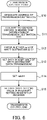
- FIG. 6 is a flowchart depicting an example flow of transmission control by the information processing system.
- the CPU 21b0 of SOC[0] designates the address in the PCIe bus space 30g0 that is associated with the address in the local DRAM space 30e1 of the memory map information 30a1 for SOC[1] (step S10).
- the CPU 21b0 designates the address so that packet_buf[0] to packet[last] depicted in FIG. 5 are accessed in ascending order. The address is designated so that after packet[last] has been accessed, packet_buf[0] is accessed.
- the address in the PCIe bus space 30g0 is converted by the MMU 21d0 to an address in the DRAM space 30e1 in the memory map information 30a1 referred to by SOC[1], which is the transmission destination (step S11).
- the CPU 21b0 checks whether the "valid" value of the write destination is 0 (step S12).
- the CPU 21b0 issues a read instruction for an address produced by conversion by the MMU 21d0.
- the CPU 21b0 then reads, via the switch 23, the value of "valid" for "packet_buf[i]" of the reception buffer region for SOC[0] that is a shared region in the DRAM 22a1 of SOC[1] corresponding to this address and checks the value.
- the CPU 21b0 may determine for example to postpone data transmission for a set period, and then terminate the transmission control when the "valid" value remains 1 after the set period.
- the CPU 21b0 sets data in "length” and “data []” (see FIG. 5 ) of the write destination (data transmission) (step S13).
- the CPU 21b0 has the data to be written into the reception buffer region as "length" and "data []” outputted to the PCIe interface together with the address converted by the MMU 21d0.
- the address and data are transferred to SOC[1] by the switch 23.
- the address is converted to the actual address in the DRAM 22a1 at the MMU 21d1 of SOC[1] and the data is written into the reception buffer region for SOC[0].
- the CPU 21b0 sets "valid" at 1 (step S14).
- the setting of valid is performed in the same way as the processing in step S13.
- the CPU 21b0 sets the interrupt setting value in the interrupt setting register of SOC[1] (step S15).
- the CPU 21b0 designates the address of the PCIe bus space 30f0 that is associated with the address of the ICU register space 30b1 of the memory map information 30a1 for SOC[1].
- the designated address is converted by the MMU 21d0 to the address of the ICU register space 30b1 of the memory map information 30a1 for SOC[1].
- the address and the interrupt setting value (for example, "1") indicating the occurrence of an interrupt are then outputted from the PCIe interface 21e0 based on control by the CPU 21b0.
- the address and interrupt setting value are transferred to SOC[1] by the switch 23.
- the address is converted to the actual address of the interrupt setting register by the MMU 21d1 of SOC[1], and the interrupt setting value is written into the interrupt setting register.
- FIG. 7 is a flowchart depicting an example flow of reception control (read control) by the information processing system.
- the CPU 21b1 of SOC[1] starts reception control (read control) on being notified of the occurrence of an interrupt from the ICU 21c1.
- the CPU 21b1 first determines whether the valid value at the read position of the reception buffer region of each SOC in the shared region of the DRAM 22a1 is 0 (step S20).
- step S21 a read process that copies the Ethernet frame data stored in the data [] field like that depicted in FIG. 5 into for example the socket buffer (indicated as sk_buff) structure of the OS (Operating System) is performed.
- the CPU 21b1 sets "valid" at 0 (step S22) and hands the socket buffer structure over to the TCP (Transmission Control Protocol)/IP stack (step S23).
- TCP Transmission Control Protocol
- step S20 it is determined whether valid is 0 for the next read position, and the same processing is repeated as above.
- SOC[0] to SOC[N] are each capable of transmission and write processing that directly designates an address.
- the information processing system 20 also makes use of the PCIe interfaces 21e0, 21e1, 21a0 to 23an+1, 24a1, and 24a2. This means that SOC[0] to SOC[N] are capable of continuously transmitting data without waiting for a response from a data transmission destination. By operating in this way, the information processing system 20 can perform processing at higher speed.
- SOC[0] to SOC[N] each directly designate an address and set an interrupt setting value.
- the SOC that is the data transmission destination determines that reception (a write) has ended and performs a read of the transmission data. By doing so, it is possible to virtually recreate Ethernet protocol where data read processing is triggered by packet reception.
- the information processing system 20 additionally includes the MMU 23b0 to 23bn+1, 24b1, and 24b2 that function as address converting circuits in the switches 23 and 24. By doing so, it is possible to convert the connection state used in communication, such as changing the write destination, without changing the configurations of SOC[0] to SOC[N].
- switches 23 and 24 on multiple stages like in FIG. 2 , it is possible to realize an information processing system 20 including a larger number of SOCs, even when there is a physical limitation on the number of SOCs that may be connected to one switch.
- FIG. 8 depicts one example of an information processing system according to a third embodiment.
- elements that are the same as the information processing system 20 according to the second embodiment depicted in FIG. 2 have been assigned the same reference numerals.
- N semiconductor integrated circuits that include the semiconductor integrated circuits 41a0 to 41an+1 are indicated as SOC[0] to SOC[N].
- the semiconductor integrated circuit 41a0 is indicated as SOC[0]
- the semiconductor integrated circuit 41a1 is indicated as SOC[1].
- At least two out of SOC[0] to SOC[N] are connected to a memory that differs to the DRAM.
- a memory 42a0 is connected to SOC[0]
- a memory 42an is connected to SOC[n]
- a memory 42an+1 is connected to SOC[n+1].
- the memories 42a0 to 42an+1 are all information storage devices that have a larger capacity than the DRAM 22a0 to 22an+1.
- the memories 42a0 to 42an+1 are SSD (Solid State Drive) memories.
- SOC[0] includes a PCIe interface 41b0.
- the PCIe interface 41b0 is connected via an MMU 41c0 to the bus 21f0. That is, the memory 42a0 is connected to the bus 21f0, in the same way as the switch 23 is connected via the PCIe interface 21e0 and the MMU 21d0 to the bus 21f0.
- the MMU 41c0 has the same functions as the MMU21d0, but when the PCIe interface 41b0 is connected to the memory 42a0, as one example, when access to the memory 42a0 (that is, a write operation or a read operation) is limited to access from the CPU 21b0 inside SOC[0], these functions may be inactivated or the MMU 41c0 itself may be omitted.
- the memory 42a0 performs a write operation or a read operation according to a command outputted by the CPU 21b0.
- the switch 23 may be connected to the PCIe interface 41b0 and the memory 42a0 may be connected to the PCIe interface 21e0.
- SOC[n], SOC[n+1], and the like have the same circuit configuration as SOC[0].
- the information processing system 40 since it is possible to increase the data size that individual SOCs are able to handle, it is possible to perform distributed processing with higher efficiency. Since the information processing system 40 is based on the information processing system 20 according to the second embodiment that is capable of high-speed processing, it is possible to make advantageous use of this ability and process large-scale data at high speed.
- FIG. 9 depicts one example of an information processing system according to a fourth embodiment.
- elements that are the same as the information processing system 40 according to the third embodiment depicted in FIG. 8 have been assigned the same reference numerals.
- a special-function LSI Large Scale Integrated circuit
- a special-function LSI 51a0 is connected to SOC[0]
- a special-function LSI 51an is connected to SOC[n]
- a special-function LSI 51an+1 is connected to SOC[n+1].
- Each of the special-function LSI 51a0 to special-function LSI 51an+1 is an LSI that performs a task with a comparatively heavy load, such as encode processing for video data, and as one example is an ASSP (Application Specific Standard Product).
- the special-function LSI 51a0 is connected via the PCIe interface 41b0, which is one example of an interface, and the MMU 41c0 to the bus 21f0.
- the MMU 41c0 has the same functions as the MMU 21d0, but when the PCIe interface 41b0 is connected to the special-function LSI 51a0, such as when operations of the special-function LSI 51a0 are limited to operations based on control signals outputted by the CPU 21b0 in SOC[0], these functions may be inactivated or the MMU 41c0 itself may be omitted.
- the switch 23 may be connected to the PCIe interface 41b0 and the special-function LSI 51a0 may be connected to the PCIe interface 21e0.
- the special-function LSI 51a0 operates based on control signals outputted by the CPU 21b0.
- the special-function LSI 51a0 is an HEVC (High Efficiency Video Coding) encoder
- the special-function LSI 51a0 receives video data from SOC[0] and generates and outputs HEVC data produced by compressing the video data.
- HEVC High Efficiency Video Coding
- the special-function LSI 51an, 51an+1, and the like are connected in the same way to SCO[n] and SOC[n+1] and operate based on control signals outputted by the CPUs of SCO[n] and SOC[n+1].
- the special-function LSIs connected to the respective SOCs perform parallel processing, it is possible to process tasks whose load is comparatively heavy, such as analysis of video data and extraction and aggregation of metadata, with higher efficiency.
- information processing system 40 according to the third embodiment and the information processing system 50 according to the fourth embodiment described above may also be combined with each other. That is, it is possible to connect memories, such as SSD memories, to certain SOCs out of SOC[0] to SOC[N] and to connect special-function LSIs to other SOCs.
- memories such as SSD memories
Landscapes
- Engineering & Computer Science (AREA)
- Theoretical Computer Science (AREA)
- Physics & Mathematics (AREA)
- General Engineering & Computer Science (AREA)
- General Physics & Mathematics (AREA)
- Mathematical Physics (AREA)
- Computer Hardware Design (AREA)
- Information Transfer Systems (AREA)
- Bus Control (AREA)
- Multi Processors (AREA)
Claims (15)
- Integrierte Halbleiterschaltung (11), die konfiguriert ist, um über einen Schalter (13) mit einem Datenübertragungsziel (12) verbunden zu werden, die integrierte Halbleiterschaltung (11) umfassend:eine Steuerschaltung (11a), die konfiguriert ist, um basierend auf ersten Speicher-Map-Informationen (11m), in denen Adressen von Speichern, definiert sind, die jeweils von einer Vielzahl von integrierten Halbleiterschaltungen verwendet werden, eine erste Adresse (a1) eines ersten Speichers (15) zuzuordnen, der mit dem Datenübertragungsziel (12) verbunden ist, das eine aus der Vielzahl von integrierten Halbleiterschaltungen ist;eine Adressumwandlungsschaltung (11c), die konfiguriert ist, um die erste Adresse (a1) in eine zweite Adresse (a3) des ersten Speichers (15) umzuwandeln, wobei die zweite Adresse (a3) in zweiten Speicher-Map-Informationen (12m) definiert ist,auf die das Datenübertragungsziel (12) verweist; undeine Busschnittstelle (11d), die konfiguriert ist, um die zweite Adresse und die Übertragungsdaten auszugeben, wobei die Busschnittstelle (11d) in der Lage ist, kontinuierlich zu übertragen, ohne auf eine Antwort von dem Datenübertragungsziel (12) zu warten.
- Integrierte Halbleiterschaltung (11) gemäß Anspruch 1, wobeiAdressen von Speicherschaltungen, in denen Interrupt-Einstellwerte in der Vielzahl von integrierten Halbleiterschaltungen eingestellt sind, in den ersten Speicher-Map-Informationen (11m) definiert sind,die Steuerschaltung (11a) konfiguriert ist, um basierend auf den ersten Speicher-Map-Informationen (11m) eine dritte Adresse einer ersten Speicherschaltung zuzuordnen, in der der Interrupt-Einstellwert an dem Datenübertragungsziel eingestellt ist,die Adressumwandlungsschaltung (11c) konfiguriert ist, um die dritte Adresse in eine vierte Adresse der ersten Speicherschaltung umzuwandeln, wobei die vierte Adresse in den zweiten Speicher-Map-Informationen (12m) definiert ist, unddie Busschnittstelle (11d) konfiguriert ist, um die vierte Adresse und den Interrupt-Einstellwert auszugeben.
- Integrierte Halbleiterschaltung (11) gemäß Anspruch 1 oder 2,
wobei die Busschnittstelle (11d) konfiguriert ist, um eine fünfte Adresse eines zweiten Speichers (14) und Schreibdaten von einer anderen integrierten Halbleiterschaltung zu empfangen, wobei die fünfte Adresse in den ersten Speicher-Map-Informationen (11m) definiert ist, und um die Schreibdaten in einen Empfangspufferbereich des zweiten Speichers (15) zuschreiben, wobei der Empfangspufferbereich entsprechend der fünften Adresse ist. - Integrierte Halbleiterschaltung (11) gemäß Anspruch 3, ferner umfassend:eine zweite Speicherschaltung, in der ein Interrupt-Einstellwert eingestellt ist,wobeidie Busschnittstelle (11d) konfiguriert ist, um eine sechste Adresse der zweiten Speicherschaltung und den Interrupt-Einstellwert zu empfangen, die von der anderen integrierten Halbleiterschaltung ausgegeben wurden, wobei die sechste Adresse in den ersten Speicher-Map-Informationen (11m) definiert ist, und um den Interrupt-Einstellwert in die zweite Speicherschaltung entsprechend der sechsten Adresse zu schreiben, unddie Steuerschaltung (11a) konfiguriert ist, um basierend auf dem Interrupt-Einstellwert zu bestimmen, ob ein Empfang der Schreibdaten beendet ist, optional, wobei die integrierte Halbleiterschaltung (11) ferner eine Interrupt-Steuerschaltung (11b) umfasst, die konfiguriert ist, um der Steuerschaltung (11a) basierend auf dem Interrupt-Einstellwert ein Interrupt-Signal bereitzustellen, das angibt, dass ein Empfang der Schreibdaten beendet ist.
- Integrierte Halbleiterschaltung (11) gemäß einem der vorherigen Ansprüche, wobei die ersten Speicher-Map-Informationen (11m) Folgendes beinhaltet:einen ersten Adressraum, der eine Adresse des zweiten Speichers (14) definiert;einen zweiten Adressraum, der eine Adresse des ersten Speichers (15) definiert;einen dritten Adressraum, der eine Adresse der zweiten Speicherschaltung definiert; undeinen vierten Adressraum, der eine Adresse der ersten Speicherschaltung definiert.
- Integrierte Halbleiterschaltung (11) gemäß einem der vorherigen Ansprüche, wobei die Busschnittstelle (11d) eine erste Busschnittstelle ist, und wobei die integrierte Halbleiterschaltung (11) ferner Folgendes umfasst:
eine zweite Busschnittstelle (41b0), die in der Lage ist, sich mit einem dritten Speicher (42a0) mit einer größeren Kapazität zu verbinden, als die Speicher, die von der Vielzahl integrierter Halbleiterschaltungen bzw. einem Sonderfunktions-LSI (51a0) verwendet werden. - Informationsverarbeitungssystem (10), umfassend:eine erste integrierte Halbleiterschaltung (11), wobei die erste integrierte Halbleiterschaltung (11) die integrierte Halbleiterschaltung (11) gemäß Anspruch 1 ist;der Schalter (13) konfiguriert ist, um die zweite Adresse (a3) und die Übertragungsdaten unter Verwendung der Busschnittstelle (11d) an das Datenübertragungsziel zu übertragen; undeine zweite integrierte Halbleiterschaltung (12), die das Datenübertragungsziel ist und konfiguriert ist, um die zweite Adresse (a3) und die Übertragungsdaten unter Verwendung der Busschnittstelle (13) zu empfangen und die Übertragungsdaten in einen Empfangspufferbereich des ersten Speichers (15) zu schreiben, wobei der Empfangspufferbereich entsprechend der zweiten Adresse (a3) ist.
- Informationsverarbeitungssystem (10) gemäß Anspruch 7, wobei:Adressen von Speicherschaltungen, in denen Interrupt-Einstellwerte in der Vielzahl von integrierten Halbleiterschaltungen eingestellt sind, in den ersten Speicher-Map-Informationen (11m) definiert sind;die Steuerschaltung (11a) konfiguriert ist, um basierend auf den ersten Speicher-Map-Informationen (11m) eine dritte Adresse einer ersten Speicherschaltung zuzuordnen, in der der Interrupt-Einstellwert an dem Datenübertragungsziel eingestellt ist;die Adressumwandlungsschaltung (11c) konfiguriert ist, um die dritte Adresse in eine vierte Adresse der ersten Speicherschaltung umzuwandeln, wobei die vierte Adresse in den zweiten Speicher-Map-Informationen (12m) definiert ist;die Busschnittstelle (11d) konfiguriert ist, um die vierte Adresse und den Interrupt-Einstellwert auszugeben;der Schalter (13) konfiguriert ist, um die vierte Adresse und den Interrupt-Einstellwert unter Verwendung der Busschnittstelle (11d) an das Datenübertragungsziel (12) zu übertragen; unddie zweite integrierte Halbleiterschaltung (12) konfiguriert ist, um die vierte Adresse und den Interrupt-Einstellwert unter Verwendung der Busschnittstelle (11d) zu empfangen, den Interrupt-Einstellwert in die erste Speicherschaltung entsprechend der vierten Adresse zu schreiben und basierend auf dem Interrupt-Einstellwert zu bestimmen, ob ein Empfang der Übertragungsdaten beendet ist,und wobei:der Schalter (13) einen ersten Schalter (23) und einen zweiten Schalter (24) beinhaltet, die konfiguriert sind, um Informationen unter Verwendung des ersten Schalters (23) und der Busschnittstelle (11d) zu senden und zu empfangen; unddie zweite Adresse, die vierte Adresse, die Übertragungsdaten und der Interrupt-Einstellwert über den ersten Schalter (23) und den zweiten Schalter (24) an die zweite integrierte Halbleiterschaltung (12) übertragen werden.
- Informationsverarbeitungssystem (10) gemäß Anspruch 8,
wobei der Schalter (13) konfiguriert ist, um die zweite Adresse und die vierte Adresse jeweils in eine fünfte Adresse eines zweiten Speichers, der mit einer dritten integrierten Halbleiterschaltung aus der Vielzahl der integrierten Halbleiterschaltungen verbunden ist, und in eine sechste Adresse einer zweiten Speicherschaltung, in der der Unterbrechungseinstellwert an der dritten integrierten Halbleiterschaltung eingestellt ist, umzuwandeln, wobei die fünfte Adresse in dritten Speicher-Map-Informationen definiert ist, auf die die dritte integrierte Halbleiterschaltung verweist. - Informationsverarbeitungssystem (10) gemäß einem der Ansprüche 7 bis 9, wobei in dem Empfangspufferbereich Pufferbereiche, die jeweils der Vielzahl von integrierten Halbleiterschaltungen entsprechen, eingestellt sind, um durch jeweils unterschiedliche Adressen zugeordnet zu werden.
- Informationsverarbeitungssystem (10) gemäß einem der Ansprüche 7 bis 10, wobei die Steuerschaltung (11a) eine erste Steuerschaltung ist,
wobei die zweite integrierte Halbleiterschaltung (12) eine zweite Steuerschaltung (12a) und eine Interrupt-Steuerschaltung (12b) beinhaltet, die konfiguriert ist, um der zweiten Steuerschaltung (12a) basierend auf dem Interrupt-Einstellwert ein Interrupt-Signal bereitzustellen, das angibt, dass ein Empfang der Übertragungsdaten beendet ist. - Informationsverarbeitungssystem (10) gemäß einem der Ansprüche 7 bis 11, wobei
die ersten Speicher-Map-Informationen (11m) Folgendes beinhalten:einen ersten Adressraum, der eine Adresse eines Speichers definiert, der mit einer integrierten Halbleiterschaltung verbunden ist, die auf die ersten Speicher-Map-Informationen aus der Vielzahl der integrierten Halbleiterschaltungen verweist;einen zweiten Adressraum, der eine Adresse eines Speichers definiert, der mit einem anderen integrierten Halbleiterschaltkreis als dem integrierten Halbleiterschaltkreis verbunden ist, der auf die ersten Speicher-Map-Informationen verweist;einen dritten Adressraum, der eine Adresse einer Speicherschaltung definiert, in der ein Interrupt-Einstellwert der integrierten Halbleiterschaltung eingestellt ist, der auf die ersten Speicher-Map-Informationen verweist; undeinen vierten Adressraum, der eine Adresse einer Speicherschaltung definiert, in der ein Interrupt-Einstellwert der anderen integrierten Halbleiterschaltung eingestellt ist. - Informationsverarbeitungssystem (10) gemäß einem der Ansprüche 7 bis 12, wobei die Busschnittstelle (11d), die in der Lage ist, kontinuierlich zu übertragen, ohne auf eine Antwort von dem Datenübertragungsziel zu warten, eine PCle (Peripheral Component Interconnect express) Schnittstelle ist.
- Informationsverarbeitungssystem (10) gemäß einem der Ansprüche 7 bis 13, wobei:
dritte Speicher mit größerer Kapazität als die Speicher, die jeweils von der Vielzahl der integrierten Halbleiterschaltungen verwendet werden mit mindestens zwei aus der Vielzahl von integrierten Halbleiterschaltungen verbunden sind; und/oder Spezialfunktions-LSIs (Large Scale Integrated Circuits) mit mindestens zwei aus der Vielzahl von integrierten Halbleiterschaltungen verbunden sind. - Informationsverarbeitungsverfahren, umfassend: Bestimmen, durch eine erste integrierte Halbleiterschaltung, die über einen Schalter mit einem Datenübertragungsziel verbunden ist, basierend auf ersten Speicherabbildungsinformationen, in denen Adressen von Speichern, die jeweils von einer Vielzahl von integrierten Halbleiterschaltungen verwendet werden, definiert sind, einer ersten Adresse eines ersten Speichers, der mit dem Datenübertragungsziel verbunden ist, das eines aus der Vielzahl von integrierten Halbleiterschaltungen ist, Umwandeln der ersten Adresse in eine zweite Adresse des ersten Speichers, wobei die zweite Adresse in zweiten Speicher-Map-Informationen definiert ist, auf die das Datenübertragungsziel verweist, und Ausgeben der zweiten Adresse und der Übertragungsdaten unter Verwendung einer Busschnittstelle, die in der Lage ist, kontinuierlich zu übertragen, ohne auf eine Antwort von dem Datenübertragungsziel zu warten;Übertragen, durch den Schalter, der zweiten Adresse und der Übertragungsdaten an das Datenübertragungsziel unter Verwendung der Busschnittstelle; undEmpfangen, durch eine zweite integrierte Halbleiterschaltung, die das Datenübertragungsziel ist, der zweiten Adresse und der Übertragungsdaten, unter Verwendung der Busschnittstelle, und Schreiben der Übertragungsdaten in einen Empfangspufferbereich des ersten Speichers, wobei der Empfangspufferbereich entsprechend der zweiten Adresse ist.
Applications Claiming Priority (2)
| Application Number | Priority Date | Filing Date | Title |
|---|---|---|---|
| JP2016232340 | 2016-11-30 | ||
| PCT/JP2017/041935 WO2018101136A1 (ja) | 2016-11-30 | 2017-11-22 | 情報処理システム、半導体集積回路及び情報処理方法 |
Publications (3)
| Publication Number | Publication Date |
|---|---|
| EP3550439A1 EP3550439A1 (de) | 2019-10-09 |
| EP3550439A4 EP3550439A4 (de) | 2019-12-11 |
| EP3550439B1 true EP3550439B1 (de) | 2022-03-30 |
Family
ID=62241380
Family Applications (1)
| Application Number | Title | Priority Date | Filing Date |
|---|---|---|---|
| EP17877100.2A Active EP3550439B1 (de) | 2016-11-30 | 2017-11-22 | Informationsverarbeitungssystem, integrierte halbleiterschaltung und informationsverarbeitungsverfahren |
Country Status (5)
| Country | Link |
|---|---|
| US (1) | US10853287B2 (de) |
| EP (1) | EP3550439B1 (de) |
| JP (2) | JP7206485B2 (de) |
| CN (1) | CN109997122B (de) |
| WO (1) | WO2018101136A1 (de) |
Families Citing this family (3)
| Publication number | Priority date | Publication date | Assignee | Title |
|---|---|---|---|---|
| US11223575B2 (en) * | 2019-12-23 | 2022-01-11 | Advanced Micro Devices, Inc. | Re-purposing byte enables as clock enables for power savings |
| CN116527714B (zh) * | 2023-05-05 | 2026-03-17 | 上汽通用汽车有限公司 | 基于PCIe的车载通信系统及车辆 |
| WO2025048515A1 (ko) * | 2023-08-29 | 2025-03-06 | 김창욱 | 버스페이지테이블 기반의 컴퓨팅 장치 연결 및 컴퓨팅 장치 사상 방법 |
Family Cites Families (15)
| Publication number | Priority date | Publication date | Assignee | Title |
|---|---|---|---|---|
| CN101027690A (zh) * | 2003-12-30 | 2007-08-29 | 美国联合包装服务有限公司 | 整合全球追踪和虚拟库存系统 |
| US7480303B1 (en) | 2005-05-16 | 2009-01-20 | Pericom Semiconductor Corp. | Pseudo-ethernet switch without ethernet media-access-controllers (MAC's) that copies ethernet context registers between PCI-express ports |
| WO2007105373A1 (ja) * | 2006-03-10 | 2007-09-20 | Sony Corporation | ブリッジ、情報処理システムおよびアクセス制御方法 |
| US7975109B2 (en) * | 2007-05-30 | 2011-07-05 | Schooner Information Technology, Inc. | System including a fine-grained memory and a less-fine-grained memory |
| US8484307B2 (en) * | 2008-02-01 | 2013-07-09 | International Business Machines Corporation | Host fabric interface (HFI) to perform global shared memory (GSM) operations |
| US8214604B2 (en) * | 2008-02-01 | 2012-07-03 | International Business Machines Corporation | Mechanisms to order global shared memory operations |
| US8180996B2 (en) * | 2008-05-15 | 2012-05-15 | Calxeda, Inc. | Distributed computing system with universal address system and method |
| WO2010005506A1 (en) * | 2008-07-10 | 2010-01-14 | Specialty Minerals (Michigan) Inc. | Wire injection lance nozzle assembly |
| EP2365445B1 (de) * | 2010-03-11 | 2013-10-23 | Ricoh Company, Ltd. | Adapter und Kommunikationsverfahren |
| JP5764919B2 (ja) * | 2010-12-16 | 2015-08-19 | 株式会社リコー | 通信機器および通信システム |
| EP2515241B1 (de) * | 2011-04-21 | 2016-05-25 | RJ Intellectual Properties, LLC | Vereintes Systembereichsnetzwerk und Schalter |
| WO2013136522A1 (ja) | 2012-03-16 | 2013-09-19 | 株式会社日立製作所 | 計算機システム及び計算機間のデータ通信方法 |
| GB2507287A (en) * | 2012-10-24 | 2014-04-30 | Ibm | Associating restore points of a program with execution states and data stored in memory. |
| US10684973B2 (en) * | 2013-08-30 | 2020-06-16 | Intel Corporation | NUMA node peripheral switch |
| JP2014160502A (ja) * | 2014-04-28 | 2014-09-04 | Fujitsu Ltd | 情報処理装置およびメモリアクセス方法 |
-
2017
- 2017-11-22 CN CN201780073022.2A patent/CN109997122B/zh active Active
- 2017-11-22 EP EP17877100.2A patent/EP3550439B1/de active Active
- 2017-11-22 JP JP2018553804A patent/JP7206485B2/ja active Active
- 2017-11-22 WO PCT/JP2017/041935 patent/WO2018101136A1/ja not_active Ceased
-
2019
- 2019-04-23 US US16/392,240 patent/US10853287B2/en active Active
-
2022
- 2022-09-21 JP JP2022149667A patent/JP7401811B2/ja active Active
Also Published As
| Publication number | Publication date |
|---|---|
| JPWO2018101136A1 (ja) | 2019-10-24 |
| JP2022176236A (ja) | 2022-11-25 |
| EP3550439A4 (de) | 2019-12-11 |
| JP7206485B2 (ja) | 2023-01-18 |
| US10853287B2 (en) | 2020-12-01 |
| JP7401811B2 (ja) | 2023-12-20 |
| US20190251049A1 (en) | 2019-08-15 |
| WO2018101136A1 (ja) | 2018-06-07 |
| EP3550439A1 (de) | 2019-10-09 |
| CN109997122A (zh) | 2019-07-09 |
| CN109997122B (zh) | 2023-06-30 |
Similar Documents
| Publication | Publication Date | Title |
|---|---|---|
| JP7774092B2 (ja) | 専用低レイテンシリンクを使用した複数のハードウェアアクセラレータのための統合されたアドレス空間 | |
| CN1647054B (zh) | 双模网络设备驱动设备、系统和方法 | |
| US6047120A (en) | Dual mode bus bridge for interfacing a host bus and a personal computer interface bus | |
| US7904629B2 (en) | Virtualized bus device | |
| JP7401811B2 (ja) | 情報処理システム、半導体集積回路及び情報処理方法 | |
| US5590292A (en) | Scalable tree structured high speed input/output subsystem architecture | |
| US20110060859A1 (en) | Host-to-host software-based virtual system | |
| CN107632953A (zh) | 一种gpu箱pcie扩展互连拓扑装置 | |
| CN105025070A (zh) | 用于优化约束系统内的网络数据流的方法 | |
| CN101889263B (zh) | 控制路径i/o虚拟化 | |
| US8090893B2 (en) | Input output control apparatus with a plurality of ports and single protocol processing circuit | |
| CN109213717B (zh) | 国产飞腾处理器的双桥片架构 | |
| KR20250095741A (ko) | 다이-간 데이터 인터페이스를 통한 다수의 엔드포인트들로의 루트 컴플렉스 스위칭 | |
| CN115543908B (zh) | 基于FPGA的Aurora总线数据交互系统 | |
| CN116450554A (zh) | 中断处理方法、根复合体设备及电子设备 | |
| US20190286606A1 (en) | Network-on-chip and computer system including the same | |
| CN114281499A (zh) | 一种总线互连时的中断传递处理方法及系统 | |
| Verma et al. | Pcie bus: A state-of-the-art-review | |
| CN218996035U (zh) | 一种配合xmda使用的rdma高速数据传输系统 | |
| US20090177832A1 (en) | Parallel computer system and method for parallel processing of data | |
| CN104699655A (zh) | 网络芯片及云服务器系统 | |
| CN209928341U (zh) | 一种支持4张显卡的服务器平衡装置 | |
| JP2009223918A (ja) | 入出力制御装置 | |
| CN121277866A (zh) | 接口装置、互联系统和芯片 | |
| CN112948317A (zh) | 基于Hlink的多节点系统及处理方法 |
Legal Events
| Date | Code | Title | Description |
|---|---|---|---|
| STAA | Information on the status of an ep patent application or granted ep patent |
Free format text: STATUS: THE INTERNATIONAL PUBLICATION HAS BEEN MADE |
|
| PUAI | Public reference made under article 153(3) epc to a published international application that has entered the european phase |
Free format text: ORIGINAL CODE: 0009012 |
|
| STAA | Information on the status of an ep patent application or granted ep patent |
Free format text: STATUS: REQUEST FOR EXAMINATION WAS MADE |
|
| 17P | Request for examination filed |
Effective date: 20190425 |
|
| AK | Designated contracting states |
Kind code of ref document: A1 Designated state(s): AL AT BE BG CH CY CZ DE DK EE ES FI FR GB GR HR HU IE IS IT LI LT LU LV MC MK MT NL NO PL PT RO RS SE SI SK SM TR |
|
| AX | Request for extension of the european patent |
Extension state: BA ME |
|
| A4 | Supplementary search report drawn up and despatched |
Effective date: 20191112 |
|
| RIC1 | Information provided on ipc code assigned before grant |
Ipc: G06F 13/40 20060101ALI20191106BHEP Ipc: G06F 13/38 20060101AFI20191106BHEP Ipc: G06F 13/42 20060101ALI20191106BHEP Ipc: G06F 13/36 20060101ALI20191106BHEP |
|
| DAV | Request for validation of the european patent (deleted) | ||
| DAX | Request for extension of the european patent (deleted) | ||
| GRAP | Despatch of communication of intention to grant a patent |
Free format text: ORIGINAL CODE: EPIDOSNIGR1 |
|
| STAA | Information on the status of an ep patent application or granted ep patent |
Free format text: STATUS: GRANT OF PATENT IS INTENDED |
|
| INTG | Intention to grant announced |
Effective date: 20211029 |
|
| GRAS | Grant fee paid |
Free format text: ORIGINAL CODE: EPIDOSNIGR3 |
|
| GRAA | (expected) grant |
Free format text: ORIGINAL CODE: 0009210 |
|
| STAA | Information on the status of an ep patent application or granted ep patent |
Free format text: STATUS: THE PATENT HAS BEEN GRANTED |
|
| AK | Designated contracting states |
Kind code of ref document: B1 Designated state(s): AL AT BE BG CH CY CZ DE DK EE ES FI FR GB GR HR HU IE IS IT LI LT LU LV MC MK MT NL NO PL PT RO RS SE SI SK SM TR |
|
| REG | Reference to a national code |
Ref country code: GB Ref legal event code: FG4D |
|
| REG | Reference to a national code |
Ref country code: CH Ref legal event code: EP |
|
| REG | Reference to a national code |
Ref country code: AT Ref legal event code: REF Ref document number: 1479845 Country of ref document: AT Kind code of ref document: T Effective date: 20220415 |
|
| REG | Reference to a national code |
Ref country code: DE Ref legal event code: R096 Ref document number: 602017055366 Country of ref document: DE |
|
| REG | Reference to a national code |
Ref country code: IE Ref legal event code: FG4D |
|
| REG | Reference to a national code |
Ref country code: LT Ref legal event code: MG9D |
|
| PG25 | Lapsed in a contracting state [announced via postgrant information from national office to epo] |
Ref country code: SE Free format text: LAPSE BECAUSE OF FAILURE TO SUBMIT A TRANSLATION OF THE DESCRIPTION OR TO PAY THE FEE WITHIN THE PRESCRIBED TIME-LIMIT Effective date: 20220330 Ref country code: RS Free format text: LAPSE BECAUSE OF FAILURE TO SUBMIT A TRANSLATION OF THE DESCRIPTION OR TO PAY THE FEE WITHIN THE PRESCRIBED TIME-LIMIT Effective date: 20220330 Ref country code: NO Free format text: LAPSE BECAUSE OF FAILURE TO SUBMIT A TRANSLATION OF THE DESCRIPTION OR TO PAY THE FEE WITHIN THE PRESCRIBED TIME-LIMIT Effective date: 20220630 Ref country code: LT Free format text: LAPSE BECAUSE OF FAILURE TO SUBMIT A TRANSLATION OF THE DESCRIPTION OR TO PAY THE FEE WITHIN THE PRESCRIBED TIME-LIMIT Effective date: 20220330 Ref country code: HR Free format text: LAPSE BECAUSE OF FAILURE TO SUBMIT A TRANSLATION OF THE DESCRIPTION OR TO PAY THE FEE WITHIN THE PRESCRIBED TIME-LIMIT Effective date: 20220330 Ref country code: BG Free format text: LAPSE BECAUSE OF FAILURE TO SUBMIT A TRANSLATION OF THE DESCRIPTION OR TO PAY THE FEE WITHIN THE PRESCRIBED TIME-LIMIT Effective date: 20220630 |
|
| REG | Reference to a national code |
Ref country code: NL Ref legal event code: MP Effective date: 20220330 |
|
| REG | Reference to a national code |
Ref country code: AT Ref legal event code: MK05 Ref document number: 1479845 Country of ref document: AT Kind code of ref document: T Effective date: 20220330 |
|
| PG25 | Lapsed in a contracting state [announced via postgrant information from national office to epo] |
Ref country code: LV Free format text: LAPSE BECAUSE OF FAILURE TO SUBMIT A TRANSLATION OF THE DESCRIPTION OR TO PAY THE FEE WITHIN THE PRESCRIBED TIME-LIMIT Effective date: 20220330 Ref country code: GR Free format text: LAPSE BECAUSE OF FAILURE TO SUBMIT A TRANSLATION OF THE DESCRIPTION OR TO PAY THE FEE WITHIN THE PRESCRIBED TIME-LIMIT Effective date: 20220701 Ref country code: FI Free format text: LAPSE BECAUSE OF FAILURE TO SUBMIT A TRANSLATION OF THE DESCRIPTION OR TO PAY THE FEE WITHIN THE PRESCRIBED TIME-LIMIT Effective date: 20220330 |
|
| PG25 | Lapsed in a contracting state [announced via postgrant information from national office to epo] |
Ref country code: NL Free format text: LAPSE BECAUSE OF FAILURE TO SUBMIT A TRANSLATION OF THE DESCRIPTION OR TO PAY THE FEE WITHIN THE PRESCRIBED TIME-LIMIT Effective date: 20220330 |
|
| PG25 | Lapsed in a contracting state [announced via postgrant information from national office to epo] |
Ref country code: SM Free format text: LAPSE BECAUSE OF FAILURE TO SUBMIT A TRANSLATION OF THE DESCRIPTION OR TO PAY THE FEE WITHIN THE PRESCRIBED TIME-LIMIT Effective date: 20220330 Ref country code: SK Free format text: LAPSE BECAUSE OF FAILURE TO SUBMIT A TRANSLATION OF THE DESCRIPTION OR TO PAY THE FEE WITHIN THE PRESCRIBED TIME-LIMIT Effective date: 20220330 Ref country code: RO Free format text: LAPSE BECAUSE OF FAILURE TO SUBMIT A TRANSLATION OF THE DESCRIPTION OR TO PAY THE FEE WITHIN THE PRESCRIBED TIME-LIMIT Effective date: 20220330 Ref country code: PT Free format text: LAPSE BECAUSE OF FAILURE TO SUBMIT A TRANSLATION OF THE DESCRIPTION OR TO PAY THE FEE WITHIN THE PRESCRIBED TIME-LIMIT Effective date: 20220801 Ref country code: ES Free format text: LAPSE BECAUSE OF FAILURE TO SUBMIT A TRANSLATION OF THE DESCRIPTION OR TO PAY THE FEE WITHIN THE PRESCRIBED TIME-LIMIT Effective date: 20220330 Ref country code: EE Free format text: LAPSE BECAUSE OF FAILURE TO SUBMIT A TRANSLATION OF THE DESCRIPTION OR TO PAY THE FEE WITHIN THE PRESCRIBED TIME-LIMIT Effective date: 20220330 Ref country code: CZ Free format text: LAPSE BECAUSE OF FAILURE TO SUBMIT A TRANSLATION OF THE DESCRIPTION OR TO PAY THE FEE WITHIN THE PRESCRIBED TIME-LIMIT Effective date: 20220330 Ref country code: AT Free format text: LAPSE BECAUSE OF FAILURE TO SUBMIT A TRANSLATION OF THE DESCRIPTION OR TO PAY THE FEE WITHIN THE PRESCRIBED TIME-LIMIT Effective date: 20220330 |
|
| PG25 | Lapsed in a contracting state [announced via postgrant information from national office to epo] |
Ref country code: PL Free format text: LAPSE BECAUSE OF FAILURE TO SUBMIT A TRANSLATION OF THE DESCRIPTION OR TO PAY THE FEE WITHIN THE PRESCRIBED TIME-LIMIT Effective date: 20220330 Ref country code: IS Free format text: LAPSE BECAUSE OF FAILURE TO SUBMIT A TRANSLATION OF THE DESCRIPTION OR TO PAY THE FEE WITHIN THE PRESCRIBED TIME-LIMIT Effective date: 20220730 Ref country code: AL Free format text: LAPSE BECAUSE OF FAILURE TO SUBMIT A TRANSLATION OF THE DESCRIPTION OR TO PAY THE FEE WITHIN THE PRESCRIBED TIME-LIMIT Effective date: 20220330 |
|
| REG | Reference to a national code |
Ref country code: DE Ref legal event code: R097 Ref document number: 602017055366 Country of ref document: DE |
|
| PG25 | Lapsed in a contracting state [announced via postgrant information from national office to epo] |
Ref country code: DK Free format text: LAPSE BECAUSE OF FAILURE TO SUBMIT A TRANSLATION OF THE DESCRIPTION OR TO PAY THE FEE WITHIN THE PRESCRIBED TIME-LIMIT Effective date: 20220330 |
|
| PLBE | No opposition filed within time limit |
Free format text: ORIGINAL CODE: 0009261 |
|
| STAA | Information on the status of an ep patent application or granted ep patent |
Free format text: STATUS: NO OPPOSITION FILED WITHIN TIME LIMIT |
|
| 26N | No opposition filed |
Effective date: 20230103 |
|
| PG25 | Lapsed in a contracting state [announced via postgrant information from national office to epo] |
Ref country code: SI Free format text: LAPSE BECAUSE OF FAILURE TO SUBMIT A TRANSLATION OF THE DESCRIPTION OR TO PAY THE FEE WITHIN THE PRESCRIBED TIME-LIMIT Effective date: 20220330 |
|
| PG25 | Lapsed in a contracting state [announced via postgrant information from national office to epo] |
Ref country code: MC Free format text: LAPSE BECAUSE OF FAILURE TO SUBMIT A TRANSLATION OF THE DESCRIPTION OR TO PAY THE FEE WITHIN THE PRESCRIBED TIME-LIMIT Effective date: 20220330 |
|
| REG | Reference to a national code |
Ref country code: CH Ref legal event code: PL |
|
| REG | Reference to a national code |
Ref country code: BE Ref legal event code: MM Effective date: 20221130 |
|
| PG25 | Lapsed in a contracting state [announced via postgrant information from national office to epo] |
Ref country code: LI Free format text: LAPSE BECAUSE OF NON-PAYMENT OF DUE FEES Effective date: 20221130 Ref country code: IT Free format text: LAPSE BECAUSE OF FAILURE TO SUBMIT A TRANSLATION OF THE DESCRIPTION OR TO PAY THE FEE WITHIN THE PRESCRIBED TIME-LIMIT Effective date: 20220330 Ref country code: CH Free format text: LAPSE BECAUSE OF NON-PAYMENT OF DUE FEES Effective date: 20221130 |
|
| PG25 | Lapsed in a contracting state [announced via postgrant information from national office to epo] |
Ref country code: LU Free format text: LAPSE BECAUSE OF NON-PAYMENT OF DUE FEES Effective date: 20221122 |
|
| PG25 | Lapsed in a contracting state [announced via postgrant information from national office to epo] |
Ref country code: IE Free format text: LAPSE BECAUSE OF NON-PAYMENT OF DUE FEES Effective date: 20221122 |
|
| PG25 | Lapsed in a contracting state [announced via postgrant information from national office to epo] |
Ref country code: BE Free format text: LAPSE BECAUSE OF NON-PAYMENT OF DUE FEES Effective date: 20221130 |
|
| PG25 | Lapsed in a contracting state [announced via postgrant information from national office to epo] |
Ref country code: HU Free format text: LAPSE BECAUSE OF FAILURE TO SUBMIT A TRANSLATION OF THE DESCRIPTION OR TO PAY THE FEE WITHIN THE PRESCRIBED TIME-LIMIT; INVALID AB INITIO Effective date: 20171122 |
|
| PG25 | Lapsed in a contracting state [announced via postgrant information from national office to epo] |
Ref country code: CY Free format text: LAPSE BECAUSE OF FAILURE TO SUBMIT A TRANSLATION OF THE DESCRIPTION OR TO PAY THE FEE WITHIN THE PRESCRIBED TIME-LIMIT Effective date: 20220330 |
|
| PG25 | Lapsed in a contracting state [announced via postgrant information from national office to epo] |
Ref country code: MK Free format text: LAPSE BECAUSE OF FAILURE TO SUBMIT A TRANSLATION OF THE DESCRIPTION OR TO PAY THE FEE WITHIN THE PRESCRIBED TIME-LIMIT Effective date: 20220330 |
|
| PG25 | Lapsed in a contracting state [announced via postgrant information from national office to epo] |
Ref country code: MT Free format text: LAPSE BECAUSE OF FAILURE TO SUBMIT A TRANSLATION OF THE DESCRIPTION OR TO PAY THE FEE WITHIN THE PRESCRIBED TIME-LIMIT Effective date: 20220330 |
|
| PG25 | Lapsed in a contracting state [announced via postgrant information from national office to epo] |
Ref country code: TR Free format text: LAPSE BECAUSE OF FAILURE TO SUBMIT A TRANSLATION OF THE DESCRIPTION OR TO PAY THE FEE WITHIN THE PRESCRIBED TIME-LIMIT Effective date: 20220330 |
|
| PGFP | Annual fee paid to national office [announced via postgrant information from national office to epo] |
Ref country code: DE Payment date: 20251119 Year of fee payment: 9 |
|
| PGFP | Annual fee paid to national office [announced via postgrant information from national office to epo] |
Ref country code: GB Payment date: 20251121 Year of fee payment: 9 |
|
| PGFP | Annual fee paid to national office [announced via postgrant information from national office to epo] |
Ref country code: FR Payment date: 20251126 Year of fee payment: 9 |