EP3547449B1 - Drahtlose kommunikationsvorrichtung, die eine mehrzahl von hornantennen auf einer leiterplatte (pcb) umfasst, entsprechendes herstellungs- und verwendungsverfahren - Google Patents
Drahtlose kommunikationsvorrichtung, die eine mehrzahl von hornantennen auf einer leiterplatte (pcb) umfasst, entsprechendes herstellungs- und verwendungsverfahren Download PDFInfo
- Publication number
- EP3547449B1 EP3547449B1 EP19164351.9A EP19164351A EP3547449B1 EP 3547449 B1 EP3547449 B1 EP 3547449B1 EP 19164351 A EP19164351 A EP 19164351A EP 3547449 B1 EP3547449 B1 EP 3547449B1
- Authority
- EP
- European Patent Office
- Prior art keywords
- pcb
- horn antenna
- plane
- wireless communication
- communication device
- Prior art date
- Legal status (The legal status is an assumption and is not a legal conclusion. Google has not performed a legal analysis and makes no representation as to the accuracy of the status listed.)
- Active
Links
Images

Classifications
-
- H—ELECTRICITY
- H01—ELECTRIC ELEMENTS
- H01Q—ANTENNAS, i.e. RADIO AERIALS
- H01Q13/00—Waveguide horns or mouths; Slot antennas; Leaky-waveguide antennas; Equivalent structures causing radiation along the transmission path of a guided wave
- H01Q13/02—Waveguide horns
- H01Q13/0275—Ridged horns
-
- H—ELECTRICITY
- H01—ELECTRIC ELEMENTS
- H01Q—ANTENNAS, i.e. RADIO AERIALS
- H01Q13/00—Waveguide horns or mouths; Slot antennas; Leaky-waveguide antennas; Equivalent structures causing radiation along the transmission path of a guided wave
- H01Q13/02—Waveguide horns
-
- H—ELECTRICITY
- H01—ELECTRIC ELEMENTS
- H01P—WAVEGUIDES; RESONATORS, LINES, OR OTHER DEVICES OF THE WAVEGUIDE TYPE
- H01P5/00—Coupling devices of the waveguide type
- H01P5/08—Coupling devices of the waveguide type for linking dissimilar lines or devices
- H01P5/10—Coupling devices of the waveguide type for linking dissimilar lines or devices for coupling balanced lines or devices with unbalanced lines or devices
- H01P5/107—Hollow-waveguide/strip-line transitions
-
- H—ELECTRICITY
- H01—ELECTRIC ELEMENTS
- H01Q—ANTENNAS, i.e. RADIO AERIALS
- H01Q1/00—Details of, or arrangements associated with, antennas
- H01Q1/12—Supports; Mounting means
- H01Q1/22—Supports; Mounting means by structural association with other equipment or articles
-
- H—ELECTRICITY
- H01—ELECTRIC ELEMENTS
- H01Q—ANTENNAS, i.e. RADIO AERIALS
- H01Q1/00—Details of, or arrangements associated with, antennas
- H01Q1/36—Structural form of radiating elements, e.g. cone, spiral, umbrella; Particular materials used therewith
-
- H—ELECTRICITY
- H01—ELECTRIC ELEMENTS
- H01Q—ANTENNAS, i.e. RADIO AERIALS
- H01Q1/00—Details of, or arrangements associated with, antennas
- H01Q1/36—Structural form of radiating elements, e.g. cone, spiral, umbrella; Particular materials used therewith
- H01Q1/38—Structural form of radiating elements, e.g. cone, spiral, umbrella; Particular materials used therewith formed by a conductive layer on an insulating support
-
- H—ELECTRICITY
- H01—ELECTRIC ELEMENTS
- H01Q—ANTENNAS, i.e. RADIO AERIALS
- H01Q13/00—Waveguide horns or mouths; Slot antennas; Leaky-waveguide antennas; Equivalent structures causing radiation along the transmission path of a guided wave
- H01Q13/02—Waveguide horns
- H01Q13/0266—Waveguide horns provided with a flange or a choke
-
- H—ELECTRICITY
- H01—ELECTRIC ELEMENTS
- H01Q—ANTENNAS, i.e. RADIO AERIALS
- H01Q13/00—Waveguide horns or mouths; Slot antennas; Leaky-waveguide antennas; Equivalent structures causing radiation along the transmission path of a guided wave
- H01Q13/02—Waveguide horns
- H01Q13/0283—Apparatus or processes specially provided for manufacturing horns
-
- H—ELECTRICITY
- H01—ELECTRIC ELEMENTS
- H01Q—ANTENNAS, i.e. RADIO AERIALS
- H01Q21/00—Antenna arrays or systems
- H01Q21/24—Combinations of antenna units polarised in different directions for transmitting or receiving circularly and elliptically polarised waves or waves linearly polarised in any direction
-
- H—ELECTRICITY
- H01—ELECTRIC ELEMENTS
- H01Q—ANTENNAS, i.e. RADIO AERIALS
- H01Q21/00—Antenna arrays or systems
- H01Q21/28—Combinations of substantially independent non-interacting antenna units or systems
Definitions
- the present invention relates to wireless communications devices with horn antenna(s), more particularly intended to ensure communications in the millimetric frequency bands.
- the invention aims more particularly to improve the integration of one or more horn antennas on a printed circuit (in English " Printed Circuit Board” acronym PCB).
- V band the frequency band of the order of 60 GHz, called V band, is a preferential solution, due to its frequency bandwidth, of the order of 10 GHz, making it possible to obtain data rates up to 6 Gbps.
- Such a speed is appreciable for making wireless links for short ranges, typically of the order of a meter, which can replace wired solutions, such as as HDMI (acronym for “ High Definition Multimedia Interface ”) or USB-C (Acronym for Universal Serial Bus Type C).
- antennas because they constitute essential components in the transmission-reception systems.
- miniaturization and performance of antennas are essential for their integration into current and future transceivers.
- a horn antenna can constitute a response to this demand by its intrinsic compactness, its good radio performance, but above all by its low losses in the millimetric frequency bands.
- a horn antenna is a guide device with progressive section consisting of a straight waveguide, for example of rectangular section, extended at one of its ends by a radiating opening of the general shape of a truncated cone or truncated pyramid.
- An advantageous type of horn antenna is one with one or more ribs inside the aperture, which increases the bandwidth of the antenna.
- the patent US4613989 discloses a detector for alerting the presence of police radars which transmit signals in the X band or the K band, which comprises a horn antenna, a PCB being attached and fixed by screwing on the top of the horn antenna.
- US5317329 describes a microwave detector with PCB comprising an electrically conductive microline on an insulating substrate, on which is mounted by screwing a horn antenna.
- US2008/007444 discloses a detector of police radar signals, in the X and K bands, in which two half-shells forming a housing are assembled to each other by screwing to house the digital PCB circuits, the two half-shells assembled forming a horn antenna.
- EP0884854 relates to a microwave guide detector with a PCB on which is fixed by screwing a metal component 12 forming a horn antenna.
- the object of the invention is to meet this need at least in part.
- the horn antenna is a surface-mounted component (CMS) via the flange(s) in plane-plane support and supported by the PCB support and fixed on the latter.
- the horn antenna is arranged with the waveguide and the radiating aperture on either side of the PCB support and with each rib in direct contact or close to a PCB track, so as to allow a direct connection or a capacitive coupling between them.
- the horn antenna is molded in one piece.
- the invention essentially consists in defining a horn antenna whose structure allows it to be produced by integral molding of a usual material, in particular a metallized plastic or a zinc-based alloy, while being of small dimensions. Its rear shape with a recess at the level of the rectangular part of the waveguide as well as its fixing flanges, allow it to be mounted like a usual surface-mounted component (CMS) vertically to the PCB and makes it perfectly compatible with the related conventional processes of setting up by "pick-and-place".
- CMS surface-mounted component
- ribs make it possible to reduce the dimensions of the radiating aperture (horn) without having to implant an additional dielectric element, to generate the two types of horizontal and vertical polarizations, and to increase the purity of polarization.
- the shape of the ribs can be easily optimized as desired to obtain the best possible performance for transmitting HF (Hyper Frequency) signals.
- the CMS mounting of the horn antenna also makes it possible to have a very reduced overall height since the radiating opening can be centered on either side of the plane of the PCB support.
- the so-called vertically polarized horn antenna has ribs arranged in the plane of symmetry of the end of its radiating aperture which is perpendicular to the plane of the PCB.
- the so-called horizontally polarized horn antenna has ribs arranged in the plane of symmetry of the end of its radiating aperture which is parallel to the plane of the PCB.
- the PCB comprises at least one notch, of complementary shapes with at least a part of the radiating opening from its small base, in which the radiating opening is recessed at least in part, the guide of right wave surrounding in the extension of the bottom of the notch at least one conductive track on the face of the PCB on which the horn antenna is mounted.
- the horn antenna is adapted to radiate in the plane of the PCB.
- the waveguide of each horn antenna has a recess, so as to give it an asymmetry.
- the horn antenna can be advantageously centered on the plane of the PCB support, so that its height (H), defined by the height of the radiating aperture, is substantially distributed for half (H/2) of either side of said support plane.
- Each horn antenna is preferably attached to the PCB support by soldering using a reflow or wave technique.
- one of the ribs of the vertically polarized horn antenna is in direct contact with a printed track while the other of the ribs is at a distance from the printed track.
- the two ribs of the horizontally polarized horn antenna being in direct contact with the two printed tracks.
- step d/ is carried out simultaneously with other surface-mounted components on the PCB.
- a wireless communication device intended to ensure transmission/reception of signals in the millimeter frequency bands, and more particularly at 60 GHz.
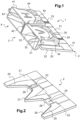
- This device 1 firstly comprises a printed circuit PCB 2 with a dielectric support 20 with two flat faces 21, 22 parallel.
- Two electrically conductive tracks 23, 24, conventionally made of copper, are made on the upper face 21 of the support 20.
- the support 20 of the PCB is advantageously provided with metal zones 25 around the end of each of the tracks 23, 24 and with two notches 26, 27 made on one edge of the support 20.
- these notches 26, 27 are in the general shape of an isosceles trapezium.
- the bottom 28, 29 of these notches is arranged near the end of each of the tracks 23, 24.
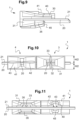
- the support 20 of the PCB supports an alternation of two horn antennas 3, 4, each molded in one piece, which are distinguished by the inner ribs 32, 33; 42, 43 they include, as explained below.
- the horn antennas 3, 4 according to the invention can advantageously be made by injection molding of a metallized plastic or even of a metal alloy.
- each antenna 3, 4 comprises a straight waveguide 30, 40 of rectangular section extended by a radiating aperture 31, 41 or horn in the form of a truncated pyramid.
- the end of each horn 31, 41 has two planes of symmetry P1, P2 perpendicular to each other.
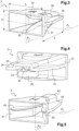
- each straight waveguide 30, 40 has an asymmetry due to a recess 35, 45 on its lower part.
- This offset 35, 45 allows vertical placement of each horn antenna on the support 20 of the PCB, advantageously compatible with a “pick & place” type assembly process.
- Two ribs 32, 33 or 42, 43 extend facing each other in one of the planes of symmetry P1, P2, over at least part of the length of the waveguide 30, 40 and of the horn 31, 41.
- Each antenna 3, 4 finally comprises peripheral zones 34, 44 around the waveguide 30, 40 and around part of the horn 31, 41. These peripheral zones 34, 44 form flanges for fixing or holding each horn antenna 3, 4 mounted in SMT surface component.
- the flanges 34, 44 are in plane-plane support and supported by the support 20 while being fixed by brazing on the metal zones 25. Indeed, during placement by pick & place, the recess 35, 45 can come into below the support 20 of the PCB, and the flanges 34, 44 come into plane-plane abutment against the upper face 21 of the support 20.
- Each horn antenna 3, 4 is embedded at least over part of the length of the horn 31, 41 in one of the notches 26, 27 of the support 20 of the PCB.
- Each horn antenna 3, 4 is arranged with the waveguide 30, 40 and the horn on either side of the support 20 of the PCB.
- the horn antenna is centered on the plane of the support 20 of the PCB so that its height H, defined by the height of the horn 31, 41, is substantially distributed for half H / 2 on either side of the plane of the support 20 of the PCB.
- one of the planes of symmetry P1 of each antenna almost coincides with the plane of the support 20 of the PCB.
- half H/2 of the height of the horn 31, 41 protrudes above the upper face 21 of the support 20 on which the antenna is mounted and the other half protrudes below the underside 22 of the support 20.
- each rib is in direct contact or close to a PCB track.
- the ribs 33, 42 and 43 of the antennas are in direct contact respectively with a track 23, 24 and 25.
- the ribs 32, 33 of one are orthogonal to the plane of the support 20 of the PCB while the ribs 42, 43 of the adjacent one are arranged in the plane of the support 20 of the PCB.
- the device 1 according to the invention which has just been described makes it possible to maintain a high or even very high bit rate, over a short transmission distance of signals in transmission or reception at 60 GHz, thanks to the juxtaposition of horn antennas with vertical polarization 3 and horizontal 4.
- each antenna is isolated from the adjacent antenna and thus allows the transmission of a data stream quite distinct from the adjacent one.
- the size of the device 1 is reduced, due on the one hand to the very small dimensions that it is possible to achieve for a horn antenna by production by molding, and on the other hand to the centering of the antenna whose horn is distributed half above the plane of the PCB support and the other half below the latter.
- L ⁇ H ⁇ l dimensions L ⁇ H ⁇ l of the order of 7 ⁇ 3.5 ⁇ 7 mm.
- the invention can also be applied to horns with a truncated cone section.
- the support 20 of the PCB is advantageously provided with notches 26, 27 of shapes complementary to those of the horn 31, 41 of the antennas 3, 4 in order to optimize the size by embedding on at least part of the horns can be provided with a less important or more important embedding.
- the opening face of the horn by which the transmission/reception of the signals is made is set back inside the PCB support.
Landscapes
- Engineering & Computer Science (AREA)
- Manufacturing & Machinery (AREA)
- Waveguide Aerials (AREA)
- Details Of Aerials (AREA)
- Transceivers (AREA)
- Variable-Direction Aerials And Aerial Arrays (AREA)
Claims (15)
- Drahtlose Kommunikationsvorrichtung (1), welche für Kommunikationen in den Millimeterfrequenzbändern bestimmt ist, umfassend:- eine Leiterplatte, PCB (2), die einen Träger (20) aus dielektrischem Material und elektrische Leiterbahnen (23, 24), die durch den dielektrischen Träger getrennt sind, umfasst,- wenigstens eine Hornantenne (3, 4), welche umfasst:● einen geraden Wellenleiter (30, 40), vorzugsweise mit rechteckigem Querschnitt, der durch eine strahlende Öffnung (31, 41) verlängert wird, wobei das Ende der strahlenden Öffnung zwei zueinander senkrechte Symmetrieebenen aufweist,● zwei Rippen (32, 33; 42, 43), die sich einander gegenüber in einer der Symmetrieebenen auf wenigstens einem Teil der Länge des Wellenleiters und der strahlenden Öffnung erstrecken,● einen oder mehrere Umfangsbereiche (34, 44) wenigstens um den Wellenleiter herum, die einen oder mehrere Befestigungsflansche bilden,wobei bei der Vorrichtung die Hornantenne ein über den oder die Flansche, die an der PCB flach anliegen und von ihr gestützt werden und auf dieser Letzteren befestigt sind, oberflächenmontiertes Bauteil (SMD) ist und die Hornantenne mit dem Wellenleiter und der strahlenden Öffnung beiderseits der PCB und mit jeder Rippe in direktem Kontakt oder in der Nähe einer Leiterbahn der PCB angeordnet ist, so dass eine direkte Verbindung oder eine kapazitive Kopplung zwischen ihnen ermöglicht wird.
- Vorrichtung nach Anspruch 1, wobei das Ende der strahlenden Öffnung einen quadratischen, rechteckigen, kreisförmigen oder elliptischen Querschnitt aufweist.
- Vorrichtung nach Anspruch 1 oder 2, wobei die Hornantenne in einem Stück geformt ist.
- Vorrichtung nach einem der vorhergehenden Ansprüche, wobei die sogenannte vertikal polarisierte Hornantenne Rippen (32, 33) aufweist, die in der Symmetrieebene (P2) angeordnet sind, welche zur Ebene der PCB (2) senkrecht ist.
- Vorrichtung nach einem der vorhergehenden Ansprüche, wobei die sogenannte horizontal polarisierte Hornantenne Rippen (32, 33) aufweist, die in der Symmetrieebene (P1) angeordnet sind, welche zur Ebene der PCB (2) parallel ist.
- Drahtlose Kommunikationsvorrichtung (1) nach einem der vorhergehenden Ansprüche, wobei die PCB wenigstens eine Aussparung (26, 27) mit Formen, die zu wenigstens einem Teil der strahlenden Öffnung von ihrer kleinen Basis aus komplementär sind, aufweist, in welche die strahlende Öffnung wenigstens teilweise eingesetzt ist, wobei der gerade Wellenleiter in der Verlängerung des Bodens (28, 29) der Aussparung wenigstens eine Leiterbahn auf der Seite der PCB, auf der die Hornantenne montiert ist, umgibt.
- Drahtlose Kommunikationsvorrichtung nach einem der vorhergehenden Ansprüche, wobei die Hornantenne dazu eingerichtet ist, in der Ebene der PCB zu strahlen.
- Drahtlose Kommunikationsvorrichtung (1) nach einem der vorhergehenden Ansprüche, wobei der Wellenleiter jeder Hornantenne (3, 4) einen Absatz (35, 45) aufweist, so dass ihm eine Asymmetrie verliehen wird.
- Drahtlose Kommunikationsvorrichtung (1) nach Anspruch 8, wobei die Hornantenne auf der Ebene des Trägers der PCB zentriert ist, so dass ihre Höhe (H), die durch die Höhe der strahlenden Öffnung definiert ist, im Wesentlichen je zur Hälfte (H/2) auf beide Seiten der Ebene des Trägers verteilt ist.
- Drahtlose Kommunikationsvorrichtung (1) nach einem der vorhergehenden Ansprüche, wobei jede Hornantenne auf dem Träger der PCB durch Löten nach einem Reflow-Verfahren oder Wellenlöten befestigt ist.
- Drahtlose Kommunikationsvorrichtung (1) nach Anspruch 4, wobei eine der Rippen der vertikal polarisierten Hornantenne in direktem Kontakt mit einer gedruckten Leiterbahn steht, während sich die andere der Rippen in einem Abstand von der gedruckten Leiterbahn befindet.
- Drahtlose Kommunikationsvorrichtung (1) nach Anspruch 5, wobei die zwei Rippen der horizontal polarisierten Hornantenne in direktem Kontakt mit den zwei gedruckten Leiterbahnen stehen.
- Drahtlose Kommunikationsvorrichtung (1) nach einem der vorhergehenden Ansprüche, welche dazu bestimmt ist, das Senden/Empfangen von Signalen mit 60 GHz sicherzustellen.
- Verfahren zur Herstellung einer drahtlosen Kommunikationsvorrichtung, welches die folgenden Schritte umfasst:a/ Bereitstellung eines Referenzdesigns einer Leiterplatte, PCB, die einen Träger aus dielektrischem Material und elektrische Leiterbahnen, die durch den dielektrischen Träger getrennt sind, umfasst;b/ Herstellung wenigstens einer Hornantenne durch integrales Formen, welche umfasst:● einen geraden Wellenleiter mit rechteckigem Querschnitt, der durch eine strahlende Öffnung verlängert wird, wobei das Ende der strahlenden Öffnung zwei zueinander senkrechte Symmetrieebenen aufweist,● zwei Rippen, die sich einander gegenüber in einer der Symmetrieebenen auf wenigstens einem Teil der Länge des Wellenleiters und der strahlenden Öffnung erstrecken,● einen oder mehrere Umfangsbereiche wenigstens um den Wellenleiter herum, die einen oder mehrere Befestigungsflansche bilden;c/ automatisches Aufsetzen der in einem Stück geformten Hornantenne auf den Träger der PCB nach einem sogenannten "Pick-and-Place" Verfahren, so dass der oder die Flansche am Träger der PCB flach anliegen und von ihm gestützt werden und auf dieser Letzteren befestigt sind und die Hornantenne mit dem Wellenleiter und der strahlenden Öffnung beiderseits des Trägers der PCB und mit jeder Rippe in direktem Kontakt oder in der Nähe einer Leiterbahn der PCB angeordnet ist, so dass eine direkte Verbindung oder eine kapazitive Kopplung zwischen ihnen ermöglicht wird;d/ Reflow-Löten oder Wellenlöten der Hornantenne.
- Herstellungsverfahren nach Anspruch 14, wobei Schritt d/ gleichzeitig mit der Oberflächenmontage anderer Bauteile auf der PCB ausgeführt wird.
Applications Claiming Priority (1)
| Application Number | Priority Date | Filing Date | Title |
|---|---|---|---|
| FR1852644A FR3079677B1 (fr) | 2018-03-27 | 2018-03-27 | Dispositif de communication sans fil integrant une pluralite d’antennes-cornets sur un circuit imprime (pcb), procede de realisation et utilisation associes |
Publications (3)
| Publication Number | Publication Date |
|---|---|
| EP3547449A1 EP3547449A1 (de) | 2019-10-02 |
| EP3547449B1 true EP3547449B1 (de) | 2023-06-07 |
| EP3547449C0 EP3547449C0 (de) | 2023-06-07 |
Family
ID=63014663
Family Applications (1)
| Application Number | Title | Priority Date | Filing Date |
|---|---|---|---|
| EP19164351.9A Active EP3547449B1 (de) | 2018-03-27 | 2019-03-21 | Drahtlose kommunikationsvorrichtung, die eine mehrzahl von hornantennen auf einer leiterplatte (pcb) umfasst, entsprechendes herstellungs- und verwendungsverfahren |
Country Status (5)
| Country | Link |
|---|---|
| EP (1) | EP3547449B1 (de) |
| KR (1) | KR102125643B1 (de) |
| CN (1) | CN110311208B (de) |
| ES (1) | ES2950129T3 (de) |
| FR (1) | FR3079677B1 (de) |
Families Citing this family (1)
| Publication number | Priority date | Publication date | Assignee | Title |
|---|---|---|---|---|
| SE2350325A1 (en) | 2023-03-23 | 2024-03-26 | Dellner Couplers Ab | Central buffer coupler, signal transceiver, vehicle member and computer-implemented method |
Family Cites Families (15)
| Publication number | Priority date | Publication date | Assignee | Title |
|---|---|---|---|---|
| US4613989A (en) * | 1984-09-28 | 1986-09-23 | Cincinnati Microwave, Inc. | Police radar warning receiver |
| JPH0693569B2 (ja) * | 1989-09-26 | 1994-11-16 | ユピテル工業株式会社 | マイクロ波検出器 |
| CN1020318C (zh) * | 1991-01-11 | 1993-04-14 | 西安电子科技大学 | 短背射横电磁波喇叭天线 |
| JP3229564B2 (ja) * | 1997-06-10 | 2001-11-19 | ユピテル工業株式会社 | マイクロ波検出器 |
| EP1050925B1 (de) * | 1998-01-22 | 2011-11-16 | Panasonic Corporation | Mehrfach-primärstrahler, abwärtsumsetzer und mehrkeulen-antenne |
| KR100423397B1 (ko) * | 2001-07-27 | 2004-03-18 | 삼성전기주식회사 | 위성방송수신장치의 듀얼 피딩시스템 |
| GB0501938D0 (en) * | 2005-02-01 | 2005-03-09 | Antenova Ltd | Balanced-unbalanced antennas for cellular radio handsets, PDAs etc |
| US7388537B2 (en) * | 2005-10-14 | 2008-06-17 | Escort Inc. | Radar detector with reduced emissions |
| US8026859B2 (en) * | 2008-08-07 | 2011-09-27 | Tdk Corporation | Horn antenna with integrated impedance matching network for improved operating frequency range |
| CN103367919B (zh) * | 2013-07-04 | 2015-09-30 | 西安电子科技大学 | 低频宽带双极化四脊喇叭天线 |
| JP6138076B2 (ja) * | 2014-03-17 | 2017-05-31 | ソニーセミコンダクタソリューションズ株式会社 | 通信装置、通信システム、及び、通信方法 |
| EP3121900B1 (de) * | 2014-04-30 | 2020-03-18 | Huawei Technologies Co. Ltd. | Leistungszuführer |
| US9692135B1 (en) * | 2015-12-10 | 2017-06-27 | Semiconductor Components Industries, Llc | Direct transition from a waveguide to a buried chip |
| CN206922020U (zh) * | 2017-05-31 | 2018-01-23 | 武汉剑通信息技术有限公司 | 一种小型化宽频喇叭天线 |
| CN107658574B (zh) * | 2017-10-27 | 2018-07-13 | 西安恒达微波技术开发有限公司 | 一种复杂电磁环境构建系统 |
-
2018
- 2018-03-27 FR FR1852644A patent/FR3079677B1/fr not_active Expired - Fee Related
-
2019
- 2019-03-21 EP EP19164351.9A patent/EP3547449B1/de active Active
- 2019-03-21 ES ES19164351T patent/ES2950129T3/es active Active
- 2019-03-27 KR KR1020190035216A patent/KR102125643B1/ko active Active
- 2019-03-27 CN CN201910234925.5A patent/CN110311208B/zh active Active
Also Published As
| Publication number | Publication date |
|---|---|
| ES2950129T3 (es) | 2023-10-05 |
| KR20190113650A (ko) | 2019-10-08 |
| EP3547449A1 (de) | 2019-10-02 |
| EP3547449C0 (de) | 2023-06-07 |
| CN110311208B (zh) | 2021-07-30 |
| KR102125643B1 (ko) | 2020-06-22 |
| FR3079677B1 (fr) | 2021-12-17 |
| FR3079677A1 (fr) | 2019-10-04 |
| CN110311208A (zh) | 2019-10-08 |
Similar Documents
| Publication | Publication Date | Title |
|---|---|---|
| EP3843202B1 (de) | Horn für eine zirkular polarisierte duale ka-band-satellitenantenne | |
| EP0899814B1 (de) | Strahlende Struktur | |
| EP1075043A1 (de) | Antenne mit übereinanderliegenden Resonanzstrukturen und Multibandfunkkommunikationsendgerät mit einer derartigen Antenne | |
| FR2625616A1 (fr) | Antenne plane | |
| EP1038333A1 (de) | Plattenantenne | |
| FR2752646A1 (fr) | Antenne imprimee plane a elements superposes court-circuites | |
| FR2800920A1 (fr) | Dispositif de transmission bi-bande et antenne pour ce dispositif | |
| FR2883671A1 (fr) | Antenne ultra-large bande offrant une grande flexibilite de conception | |
| EP3840115A1 (de) | Kompakte antenne mit resonanzhohlraum | |
| WO2000014825A9 (fr) | Antenne | |
| EP3258543A1 (de) | Wlan-kompaktantenne mit reflektor aus metamaterial | |
| EP3547449B1 (de) | Drahtlose kommunikationsvorrichtung, die eine mehrzahl von hornantennen auf einer leiterplatte (pcb) umfasst, entsprechendes herstellungs- und verwendungsverfahren | |
| EP2532049B1 (de) | Gefaltete zweipolige planarantenne | |
| EP2404344B1 (de) | Vorrichtung zur montage einer antenne | |
| EP1181744B1 (de) | Antenne mit vertikaler polarisation | |
| FR2914113A1 (fr) | Antenne mixte | |
| EP4222811A1 (de) | Hochfrequenzverbinder | |
| EP1518296B1 (de) | Mehrband-planarantenne | |
| WO2006125925A1 (fr) | Antenne monopole | |
| EP3031097B1 (de) | Vorrichtung zum senden und/oder empfangen von hochfrequenzsignalen | |
| EP0929914B1 (de) | Hochfrequenzantenne | |
| EP3266064A1 (de) | Omnidirektionale breitbandantennenstruktur | |
| EP4485687B1 (de) | Durch hindernisvorspannung anpassbares strahlungsdiagramm | |
| WO2015189136A1 (fr) | Antenne plate de telecommunication par satellite | |
| FR3007213A1 (fr) | Procede pour radioelectrifier un objet installe dans un espace public et objet ainsi radioelectrifie. |
Legal Events
| Date | Code | Title | Description |
|---|---|---|---|
| PUAI | Public reference made under article 153(3) epc to a published international application that has entered the european phase |
Free format text: ORIGINAL CODE: 0009012 |
|
| STAA | Information on the status of an ep patent application or granted ep patent |
Free format text: STATUS: REQUEST FOR EXAMINATION WAS MADE |
|
| 17P | Request for examination filed |
Effective date: 20190321 |
|
| AK | Designated contracting states |
Kind code of ref document: A1 Designated state(s): AL AT BE BG CH CY CZ DE DK EE ES FI FR GB GR HR HU IE IS IT LI LT LU LV MC MK MT NL NO PL PT RO RS SE SI SK SM TR |
|
| AX | Request for extension of the european patent |
Extension state: BA ME |
|
| STAA | Information on the status of an ep patent application or granted ep patent |
Free format text: STATUS: EXAMINATION IS IN PROGRESS |
|
| 17Q | First examination report despatched |
Effective date: 20210609 |
|
| GRAP | Despatch of communication of intention to grant a patent |
Free format text: ORIGINAL CODE: EPIDOSNIGR1 |
|
| STAA | Information on the status of an ep patent application or granted ep patent |
Free format text: STATUS: GRANT OF PATENT IS INTENDED |
|
| INTG | Intention to grant announced |
Effective date: 20221026 |
|
| GRAS | Grant fee paid |
Free format text: ORIGINAL CODE: EPIDOSNIGR3 |
|
| GRAA | (expected) grant |
Free format text: ORIGINAL CODE: 0009210 |
|
| STAA | Information on the status of an ep patent application or granted ep patent |
Free format text: STATUS: THE PATENT HAS BEEN GRANTED |
|
| AK | Designated contracting states |
Kind code of ref document: B1 Designated state(s): AL AT BE BG CH CY CZ DE DK EE ES FI FR GB GR HR HU IE IS IT LI LT LU LV MC MK MT NL NO PL PT RO RS SE SI SK SM TR |
|
| REG | Reference to a national code |
Ref country code: GB Ref legal event code: FG4D Free format text: NOT ENGLISH |
|
| REG | Reference to a national code |
Ref country code: CH Ref legal event code: EP Ref country code: AT Ref legal event code: REF Ref document number: 1577705 Country of ref document: AT Kind code of ref document: T Effective date: 20230615 |
|
| REG | Reference to a national code |
Ref country code: DE Ref legal event code: R096 Ref document number: 602019029727 Country of ref document: DE |
|
| U01 | Request for unitary effect filed |
Effective date: 20230607 |
|
| U07 | Unitary effect registered |
Designated state(s): AT BE BG DE DK EE FI FR IT LT LU LV MT NL PT SE SI Effective date: 20230612 |
|
| REG | Reference to a national code |
Ref country code: LT Ref legal event code: MG9D |
|
| REG | Reference to a national code |
Ref country code: ES Ref legal event code: FG2A Ref document number: 2950129 Country of ref document: ES Kind code of ref document: T3 Effective date: 20231005 |
|
| PG25 | Lapsed in a contracting state [announced via postgrant information from national office to epo] |
Ref country code: NO Free format text: LAPSE BECAUSE OF FAILURE TO SUBMIT A TRANSLATION OF THE DESCRIPTION OR TO PAY THE FEE WITHIN THE PRESCRIBED TIME-LIMIT Effective date: 20230907 |
|
| PG25 | Lapsed in a contracting state [announced via postgrant information from national office to epo] |
Ref country code: RS Free format text: LAPSE BECAUSE OF FAILURE TO SUBMIT A TRANSLATION OF THE DESCRIPTION OR TO PAY THE FEE WITHIN THE PRESCRIBED TIME-LIMIT Effective date: 20230607 Ref country code: HR Free format text: LAPSE BECAUSE OF FAILURE TO SUBMIT A TRANSLATION OF THE DESCRIPTION OR TO PAY THE FEE WITHIN THE PRESCRIBED TIME-LIMIT Effective date: 20230607 Ref country code: GR Free format text: LAPSE BECAUSE OF FAILURE TO SUBMIT A TRANSLATION OF THE DESCRIPTION OR TO PAY THE FEE WITHIN THE PRESCRIBED TIME-LIMIT Effective date: 20230908 |
|
| PG25 | Lapsed in a contracting state [announced via postgrant information from national office to epo] |
Ref country code: SK Free format text: LAPSE BECAUSE OF FAILURE TO SUBMIT A TRANSLATION OF THE DESCRIPTION OR TO PAY THE FEE WITHIN THE PRESCRIBED TIME-LIMIT Effective date: 20230607 |
|
| PG25 | Lapsed in a contracting state [announced via postgrant information from national office to epo] |
Ref country code: IS Free format text: LAPSE BECAUSE OF FAILURE TO SUBMIT A TRANSLATION OF THE DESCRIPTION OR TO PAY THE FEE WITHIN THE PRESCRIBED TIME-LIMIT Effective date: 20231007 |
|
| PG25 | Lapsed in a contracting state [announced via postgrant information from national office to epo] |
Ref country code: SM Free format text: LAPSE BECAUSE OF FAILURE TO SUBMIT A TRANSLATION OF THE DESCRIPTION OR TO PAY THE FEE WITHIN THE PRESCRIBED TIME-LIMIT Effective date: 20230607 Ref country code: SK Free format text: LAPSE BECAUSE OF FAILURE TO SUBMIT A TRANSLATION OF THE DESCRIPTION OR TO PAY THE FEE WITHIN THE PRESCRIBED TIME-LIMIT Effective date: 20230607 Ref country code: RO Free format text: LAPSE BECAUSE OF FAILURE TO SUBMIT A TRANSLATION OF THE DESCRIPTION OR TO PAY THE FEE WITHIN THE PRESCRIBED TIME-LIMIT Effective date: 20230607 Ref country code: IS Free format text: LAPSE BECAUSE OF FAILURE TO SUBMIT A TRANSLATION OF THE DESCRIPTION OR TO PAY THE FEE WITHIN THE PRESCRIBED TIME-LIMIT Effective date: 20231007 Ref country code: CZ Free format text: LAPSE BECAUSE OF FAILURE TO SUBMIT A TRANSLATION OF THE DESCRIPTION OR TO PAY THE FEE WITHIN THE PRESCRIBED TIME-LIMIT Effective date: 20230607 |
|
| PG25 | Lapsed in a contracting state [announced via postgrant information from national office to epo] |
Ref country code: PL Free format text: LAPSE BECAUSE OF FAILURE TO SUBMIT A TRANSLATION OF THE DESCRIPTION OR TO PAY THE FEE WITHIN THE PRESCRIBED TIME-LIMIT Effective date: 20230607 |
|
| REG | Reference to a national code |
Ref country code: DE Ref legal event code: R097 Ref document number: 602019029727 Country of ref document: DE |
|
| U20 | Renewal fee for the european patent with unitary effect paid |
Year of fee payment: 6 Effective date: 20240220 |
|
| PLBE | No opposition filed within time limit |
Free format text: ORIGINAL CODE: 0009261 |
|
| STAA | Information on the status of an ep patent application or granted ep patent |
Free format text: STATUS: NO OPPOSITION FILED WITHIN TIME LIMIT |
|
| 26N | No opposition filed |
Effective date: 20240308 |
|
| PG25 | Lapsed in a contracting state [announced via postgrant information from national office to epo] |
Ref country code: MC Free format text: LAPSE BECAUSE OF FAILURE TO SUBMIT A TRANSLATION OF THE DESCRIPTION OR TO PAY THE FEE WITHIN THE PRESCRIBED TIME-LIMIT Effective date: 20230607 |
|
| PG25 | Lapsed in a contracting state [announced via postgrant information from national office to epo] |
Ref country code: MC Free format text: LAPSE BECAUSE OF FAILURE TO SUBMIT A TRANSLATION OF THE DESCRIPTION OR TO PAY THE FEE WITHIN THE PRESCRIBED TIME-LIMIT Effective date: 20230607 |
|
| PG25 | Lapsed in a contracting state [announced via postgrant information from national office to epo] |
Ref country code: IE Free format text: LAPSE BECAUSE OF NON-PAYMENT OF DUE FEES Effective date: 20240321 |
|
| PG25 | Lapsed in a contracting state [announced via postgrant information from national office to epo] |
Ref country code: IE Free format text: LAPSE BECAUSE OF NON-PAYMENT OF DUE FEES Effective date: 20240321 |
|
| U20 | Renewal fee for the european patent with unitary effect paid |
Year of fee payment: 7 Effective date: 20250210 |
|
| PGFP | Annual fee paid to national office [announced via postgrant information from national office to epo] |
Ref country code: ES Payment date: 20250401 Year of fee payment: 7 |
|
| PGFP | Annual fee paid to national office [announced via postgrant information from national office to epo] |
Ref country code: CH Payment date: 20250401 Year of fee payment: 7 |
|
| PG25 | Lapsed in a contracting state [announced via postgrant information from national office to epo] |
Ref country code: CY Free format text: LAPSE BECAUSE OF FAILURE TO SUBMIT A TRANSLATION OF THE DESCRIPTION OR TO PAY THE FEE WITHIN THE PRESCRIBED TIME-LIMIT; INVALID AB INITIO Effective date: 20190321 |
|
| PG25 | Lapsed in a contracting state [announced via postgrant information from national office to epo] |
Ref country code: HU Free format text: LAPSE BECAUSE OF FAILURE TO SUBMIT A TRANSLATION OF THE DESCRIPTION OR TO PAY THE FEE WITHIN THE PRESCRIBED TIME-LIMIT; INVALID AB INITIO Effective date: 20190321 |
|
| U1N | Appointed representative for the unitary patent procedure changed after the registration of the unitary effect |
Representative=s name: IPSILON; FR |
|
| PG25 | Lapsed in a contracting state [announced via postgrant information from national office to epo] |
Ref country code: TR Free format text: LAPSE BECAUSE OF FAILURE TO SUBMIT A TRANSLATION OF THE DESCRIPTION OR TO PAY THE FEE WITHIN THE PRESCRIBED TIME-LIMIT Effective date: 20230607 |
|
| U20 | Renewal fee for the european patent with unitary effect paid |
Year of fee payment: 8 Effective date: 20260219 |
|
| REG | Reference to a national code |
Ref country code: CH Ref legal event code: U11 Free format text: ST27 STATUS EVENT CODE: U-0-0-U10-U11 (AS PROVIDED BY THE NATIONAL OFFICE) Effective date: 20260401 |
|
| PGFP | Annual fee paid to national office [announced via postgrant information from national office to epo] |
Ref country code: GB Payment date: 20260219 Year of fee payment: 8 |