EP3547337A1 - Positionierungs- und montagehilfe für spulen auf leiterplatten - Google Patents
Positionierungs- und montagehilfe für spulen auf leiterplatten Download PDFInfo
- Publication number
- EP3547337A1 EP3547337A1 EP19160728.2A EP19160728A EP3547337A1 EP 3547337 A1 EP3547337 A1 EP 3547337A1 EP 19160728 A EP19160728 A EP 19160728A EP 3547337 A1 EP3547337 A1 EP 3547337A1
- Authority
- EP
- European Patent Office
- Prior art keywords
- circuit board
- printed circuit
- spacer
- component
- inductive component
- Prior art date
- Legal status (The legal status is an assumption and is not a legal conclusion. Google has not performed a legal analysis and makes no representation as to the accuracy of the status listed.)
- Granted
Links
Images



Classifications
-
- H—ELECTRICITY
- H01—ELECTRIC ELEMENTS
- H01F—MAGNETS; INDUCTANCES; TRANSFORMERS; SELECTION OF MATERIALS FOR THEIR MAGNETIC PROPERTIES
- H01F27/00—Details of transformers or inductances, in general
- H01F27/02—Casings
- H01F27/027—Casings specially adapted for combination of signal type inductors or transformers with electronic circuits, e.g. mounting on printed circuit boards
-
- H—ELECTRICITY
- H01—ELECTRIC ELEMENTS
- H01F—MAGNETS; INDUCTANCES; TRANSFORMERS; SELECTION OF MATERIALS FOR THEIR MAGNETIC PROPERTIES
- H01F27/00—Details of transformers or inductances, in general
- H01F27/06—Mounting, supporting or suspending transformers, reactors or choke coils not being of the signal type
-
- H—ELECTRICITY
- H01—ELECTRIC ELEMENTS
- H01F—MAGNETS; INDUCTANCES; TRANSFORMERS; SELECTION OF MATERIALS FOR THEIR MAGNETIC PROPERTIES
- H01F27/00—Details of transformers or inductances, in general
- H01F27/28—Coils; Windings; Conductive connections
- H01F27/29—Terminals; Tapping arrangements for signal inductances
-
- H—ELECTRICITY
- H01—ELECTRIC ELEMENTS
- H01H—ELECTRIC SWITCHES; RELAYS; SELECTORS; EMERGENCY PROTECTIVE DEVICES
- H01H1/00—Contacts
- H01H1/58—Electric connections to or between contacts; Terminals
- H01H1/5805—Connections to printed circuits
-
- H—ELECTRICITY
- H05—ELECTRIC TECHNIQUES NOT OTHERWISE PROVIDED FOR
- H05K—PRINTED CIRCUITS; CASINGS OR CONSTRUCTIONAL DETAILS OF ELECTRIC APPARATUS; MANUFACTURE OF ASSEMBLAGES OF ELECTRICAL COMPONENTS
- H05K1/00—Printed circuits
- H05K1/18—Printed circuits structurally associated with non-printed electric components
- H05K1/182—Printed circuits structurally associated with non-printed electric components associated with components mounted in printed circuit boards [PCB], e.g. insert-mounted components [IMC]
- H05K1/184—Printed circuits structurally associated with non-printed electric components associated with components mounted in printed circuit boards [PCB], e.g. insert-mounted components [IMC] associated with components inserted in holes through the PCBs and wherein terminals of the components are connected to printed contacts on the walls of the holes or at the edges thereof or protruding over or into the holes
-
- H—ELECTRICITY
- H05—ELECTRIC TECHNIQUES NOT OTHERWISE PROVIDED FOR
- H05K—PRINTED CIRCUITS; CASINGS OR CONSTRUCTIONAL DETAILS OF ELECTRIC APPARATUS; MANUFACTURE OF ASSEMBLAGES OF ELECTRICAL COMPONENTS
- H05K3/00—Apparatus or processes for manufacturing printed circuits
- H05K3/30—Assembling printed circuits with electric components, e.g. with resistors
- H05K3/301—Assembling printed circuits with electric components, e.g. with resistors by means of a mounting structure
-
- H—ELECTRICITY
- H05—ELECTRIC TECHNIQUES NOT OTHERWISE PROVIDED FOR
- H05K—PRINTED CIRCUITS; CASINGS OR CONSTRUCTIONAL DETAILS OF ELECTRIC APPARATUS; MANUFACTURE OF ASSEMBLAGES OF ELECTRICAL COMPONENTS
- H05K3/00—Apparatus or processes for manufacturing printed circuits
- H05K3/30—Assembling printed circuits with electric components, e.g. with resistors
- H05K3/306—Assembling printed circuits with electric components, e.g. with resistors with lead-in-hole components
-
- H—ELECTRICITY
- H01—ELECTRIC ELEMENTS
- H01F—MAGNETS; INDUCTANCES; TRANSFORMERS; SELECTION OF MATERIALS FOR THEIR MAGNETIC PROPERTIES
- H01F27/00—Details of transformers or inductances, in general
- H01F27/06—Mounting, supporting or suspending transformers, reactors or choke coils not being of the signal type
- H01F2027/065—Mounting on printed circuit boards
-
- H—ELECTRICITY
- H01—ELECTRIC ELEMENTS
- H01F—MAGNETS; INDUCTANCES; TRANSFORMERS; SELECTION OF MATERIALS FOR THEIR MAGNETIC PROPERTIES
- H01F27/00—Details of transformers or inductances, in general
- H01F27/28—Coils; Windings; Conductive connections
- H01F27/29—Terminals; Tapping arrangements for signal inductances
- H01F2027/297—Terminals; Tapping arrangements for signal inductances with pin-like terminal to be inserted in hole of printed path
-
- H—ELECTRICITY
- H05—ELECTRIC TECHNIQUES NOT OTHERWISE PROVIDED FOR
- H05K—PRINTED CIRCUITS; CASINGS OR CONSTRUCTIONAL DETAILS OF ELECTRIC APPARATUS; MANUFACTURE OF ASSEMBLAGES OF ELECTRICAL COMPONENTS
- H05K2201/00—Indexing scheme relating to printed circuits covered by H05K1/00
- H05K2201/10—Details of components or other objects attached to or integrated in a printed circuit board
- H05K2201/10007—Types of components
- H05K2201/1003—Non-printed inductor
Definitions
- the present invention relates to an inductive component, such as a coil, a transformer or transformer, for soldering to a printed circuit board and a printed circuit board with such an inductive component.
- an inductive component such as a coil, a transformer or transformer
- the coils are the components which have a great influence on the size of the printed circuit board, in particular its thickness.
- the circuit boards equipped with components should be as flat as possible.
- Low profile coils, however, are expensive.
- large coils usually have to be soldered by hand on the circuit board, whereby the positioning for the soldering is difficult.
- the invention has for its object to provide devices that reduce the problems described.
- it is an object to provide an inductive component which permits a low overall height of the printed circuit board equipped with it and can be easily soldered to a printed circuit board and to provide a printed circuit board with an inductive component which has a low overall height.
- an inductive component provided for soldering onto a printed circuit board has laterally arranged connecting wires, wherein a spacer for positioning the component on the printed circuit board with respect to the height is arranged on at least one of the connecting wires.
- the spacer held by the terminal wire is supported on the circuit board in a direction perpendicular to the circuit board when the device is mounted on the circuit board for soldering.
- the inductive component is before and after soldering by means of the spacer on the circuit board and is positioned by this at least in height.
- the component can be used in a section of the printed circuit board, an opening provided for the component, wherein the height at which the component protrudes from the opening, by means of the spacer is definable.
- the spacer may have a bore through which the connection wire passes.
- the protruding end of the terminal wire may be bent in the direction of the printed circuit board, so that slippage of the spacer is prevented by the connecting wire and at the same time the height offset is compensated during mounting on the circuit board.
- the spacer may have at least one shoulder, by means of which the spacer is supported on the printed circuit board in the horizontal direction when the component is introduced for soldering in a section of the printed circuit board, which gives the arrangement additional mechanical stability.
- connection wires can be arranged on opposite sides of the component, wherein a spacer is held on each of the opposite sides by the connection wires.
- the inductive component for soldering to a printed circuit board, a housing and at least one arranged on the housing spacers, wherein the spacer the device positioned on the circuit board with respect to the height in which the spacer on the circuit board in supported vertical direction when the device is mounted on the circuit board for soldering.
- the inductive component is before and after soldering by means of the spacer on the circuit board and is positioned by this at least in height.
- the component can be used in a section of the printed circuit board, an opening provided for the component, wherein the height at which the component protrudes from the opening, by means of the spacer is definable. This simplifies the soldering of the device in the desired position and allows a lower total height of the assembled with the inductive component circuit board.
- At least one spacer may be part of the housing or molded on the housing.
- the spacer may be an edge or a projection on the housing, which is supported on the circuit board in the vertical direction when the device is mounted for soldering to the circuit board. Since the spacer is integrated in the housing, no additional component is needed.
- the spacer or other spacer disposed on the housing may be a sleeve or cap attached to the housing.
- connection wires may be arranged on opposite sides of the component, the spacer being supported in each case between the opposite sides on the printed circuit board in the vertical direction when the component is placed on the printed circuit board for soldering.
- the inductive component may be a planar coil or a planar transformer.
- a printed circuit board has at least one of the inductive components described, wherein the printed circuit board can have a cutout in which the inductive component is arranged.
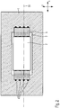
- Fig. 1 shows a sectional view (section line S1 in Fig. 2 ) of a printed circuit board 1, on which an inductive component 2 according to the present invention is soldered.
- the cuboidal component 2 protrudes from above into a cutout 3 of the circuit board 1 and has four connection wires 4 on two of its opposite narrow sides. On each of the narrow sides is a plugged onto the connecting wires 4 spacer 5.
- the protruding from the spacers 5 ends of the connecting wires 4 are bent in the direction of the circuit board 1 down, passed through the circuit board 1 and soldered.
- the lead wires are led out on one side of the device, which facilitates the winding of such a coil, yet to achieve a height-centered mounting position in the circuit board.
- Fig. 2 In a view from above, the printed circuit board 1 with the component 2 located in the cutout 3.
- the total height h G of the printed circuit board 1 equipped with components 2 can be reduced by the height of the unpopulated printed circuit board 1 be avoided and in particular the one-sided large height through the coil.
- the distance d A is chosen so that the component 2 and the circuit board 1 are centered or have the same center line.
- the distance d A can also be selected as needed so that the lower surface of the component 2 and the lower surface of the circuit board 1 lie in a plane.
- Fig. 3a shows a pushed onto the four connecting wires 4 spacer 5, in which four through holes 6 are arranged centrally in height. Through these through-holes 6, the four lead wires 4 are guided, and the ends of the lead wires 4 projecting from the through holes 6 are bent toward the printed circuit board 1, fixing the spacer 5 on the lead wires 4.
- the spacer 5 consists of a solid and electrically insulating material, such as the plastic PVC.
- Fig. 3b shows another embodiment of the spacer 5, in which 4 recesses 7 (notches) are provided for receiving the bent ends of the connecting wires.
- the depressions 7 can serve as a bending aid / guide and can be closed after bending, including the connection wires 4. It is also possible to provide 5 recesses 7 (notches, grooves) instead of the through holes 6 on the upper side of the spacer.
- connection wires 4 are not passed through the circuit board 1 but lie during soldering on the top of the circuit board 1 on.
- the spacers 5 have on their underside a shoulder 8, by means of which the component 2 is positioned in the horizontal direction (x-direction) relative to the printed circuit board 1.
- a further shoulder may be provided on the underside, by means of which the component 2 in the in Fig. 1 positioned x-direction is positioned.
- Fig. 5 shows a printed circuit board 1 with an inductive component 2 according to a third embodiment according to the present invention in the view from above.
- the spacer 5a is designed as a cap pushed onto the cuboidal component 2 or its housing from below. Before inserting the inductive component 2 into the cutout 3, the spacer 5a can be attached to the housing by force or positive engagement or can be arranged only in the cutout 3 and then slid into the cutout 3 simultaneously with the insertion of the inductive component 2.
- Fig. 6 shows a sectional view according to the in Fig. 5 shown section line S2.
- the spacer 5a at its upper end on the longitudinal sides in each case a paragraph 9 (thickening), with which the spacer 5a in the vertical direction (z) is supported downwards.
- the vertical position of the heel 9 (the edge) with respect to the printed circuit board 1 and the component 2 determines the height h B at which the component 2 protrudes downward (or upwards) from the printed circuit board 1 and can vary depending on the application / need become.
- the spacer 5a also in the horizontal direction (y) on the circuit board 1, so that in this case also a horizontal positioning of the component 2 with respect to the circuit board 1 takes place.
- the spacer 5a as a sleeve, in which at least a part of the underside of the component 2 and possibly also parts of the side surfaces of the Component 2 are exposed.
- the heel 9 (the edge) may be formed on the housing or be part of the part of the housing.
- the housing of the component 2 may be made of a plastic by injection molding.
- Fig. 7 shows a side view in the y-direction (no sectional view) of in Fig. 5 shown circuit board 1, wherein the horizontal position of the cutout 3 is indicated by the dashed line.
- the spacer 5a does not abut against the connection wires 4 located on the short sides of the component 2.
Landscapes
- Engineering & Computer Science (AREA)
- Power Engineering (AREA)
- Microelectronics & Electronic Packaging (AREA)
- Manufacturing & Machinery (AREA)
- Physics & Mathematics (AREA)
- Electromagnetism (AREA)
- Structures For Mounting Electric Components On Printed Circuit Boards (AREA)
Abstract
Description
- Die vorliegende Erfindung betrifft ein induktives Bauelement, wie eine Spule, einen Übertrager oder Transformator, zum Einlöten auf eine Leiterplatte und eine Leiterplatte mit einem solchen induktiven Bauelement.
- Von den auf Leiterplatten befindlichen Bauelementen sind die Spulen die Bauelemente, welche einen großen Einfluss auf die Baugröße der Leiterplatte insbesondere deren Dicke haben. Bei vielen Anwendungen sollen die mit Bauelementen bestückten Leiterplatten möglichst flach sein. Spulen mit geringer Bauhöhe sind jedoch teuer. Zudem müssen große Spulen meist von Hand auf der Leiterplatte verlötet werden, wobei die Positionierung für das Löten schwierig ist.
- Der Erfindung liegt die Aufgabe zugrunde, Vorrichtungen anzugeben, die die beschriebenen Probleme verringern. Aufgabe ist es insbesondere, ein induktives Bauelement bereitzustellen, das eine niedrige Bauhöhe der mit ihm bestückten Leiterplatte erlaubt und einfach auf eine Leiterplatte aufgelötet werden kann sowie eine Leiterplatte mit einem induktiven Bauelement bereitzustellen, die eine niedrige Bauhöhe aufweist.
- Diese Aufgabe wird gemäß den Merkmalen der unabhängigen Ansprüche gelöst. Die Erfindung wird durch die Merkmale der abhängigen Ansprüche weitergebildet.
- Gemäß der vorliegenden Erfindung weist ein zum Einlöten auf eine Leiterplatte vorgesehenes induktives Bauelement seitlich angeordnete Anschluss-Drähte auf, wobei an zumindest einem der Anschluss-Drähte ein Abstandhalter zum Positionieren des Bauelements auf der Leiterplatte bezüglich der Höhe angeordnet ist. Der von dem Anschluss-Draht gehaltene Abstandhalter stützt sich an der Leiterplatte in einer Richtung senkrecht zur Leiterplatte ab, wenn das Bauelement zum Einlöten auf die Leiterplatte aufgesetzt wird. Das induktive Bauelement liegt vor und nach dem Löten mittels des Abstandhalters auf der Leiterplatte auf und wird durch diesen zumindest in der Höhe positioniert. Das Bauelement kann in einem Ausschnitt der Leiterplatte, einer für das Bauelement vorgesehenen Öffnung einsetzt werden, wobei die Höhe, mit der das Bauelement aus der Öffnung ragt, mittels des Abstandhalters definierbar ist. Dies vereinfacht das Verlöten des Bauelements in der gewünschten Position und erlaubt eine geringere Gesamt-Bauhöhe der mit dem induktiven Bauelement bestückten Leiterplatte. Da nur Abstandhalter an den bereits vorhandenen Anschluss-Drähten angebracht werden müssen, ist keine Änderung/Anpassung des Bauelements nötig. Durch Verwendung unterschiedlicher Abstandshalter lassen sich für ein Bauelement nach Bedarf unterschiedliche Einbaulagen realisieren.
- Zur Befestigung kann der Abstandhalter eine Bohrung, durch die der Anschluss-Draht hindurchführt, aufweisen.
- Zusätzlich kann das aus der Bohrung ragende Ende des Anschluss-Drahts in Richtung der Leiterplatte gebogen sein, so dass ein Abgleiten des Abstandhalters vom Anschluss-Draht verhindert wird und gleichzeitig der Höhenversatz bei der Montage auf der Leiterplatte kompensiert wird.
- Alternativ oder zusätzlich kann der Abstandhalter zumindest einen Absatz aufweisen, mittels dem sich der Abstandhalter an der Leiterplatte in horizontaler Richtung abstützt, wenn das Bauelement zum Einlöten in einen Ausschnitt der Leiterplatte eingeführt ist, was der Anordnung zusätzliche mechanische Stabilität verleiht.
- Alternativ oder zusätzlich können an gegenüberliegenden Seiten des Bauelements Anschluss-Drähte angeordnet sein, wobei jeweils ein Abstandhalter an jeder den gegenüberliegenden Seiten von den Anschluss-Drähten gehalten wird.
- Gemäß einer Ausführung der vorliegenden Erfindung weist das induktive Bauelement zum Einlöten auf eine Leiterplatte, ein Gehäuse und zumindest ein an dem Gehäuse angeordneten Abstandhalter auf, wobei der Abstandhalter das Bauelement auf der Leiterplatte bezüglich der Höhe positioniert, in dem sich der Abstandhalter an der Leiterplatte in vertikaler Richtung abstützt, wenn das Bauelement zum Einlöten auf die Leiterplatte aufgesetzt ist. Das induktive Bauelement liegt vor und nach dem Löten mittels des Abstandhalters auf der Leiterplatte auf und wird durch diesen zumindest in der Höhe positioniert. Das Bauelement kann in einem Ausschnitt der Leiterplatte, einer für das Bauelement vorgesehenen Öffnung einsetzt werden, wobei die Höhe, mit der das Bauelement aus der Öffnung ragt, mittels des Abstandhalters definierbar ist. Dies vereinfacht das Verlöten des Bauelements in der gewünschten Position und erlaubt eine geringere Gesamt-Bauhöhe der mit dem induktiven Bauelement bestückten Leiterplatte.
- Zumindest ein Abstandhalter kann Teil des Gehäuses bzw. an dem Gehäuse abgeformt sein. Beispielsweise kann der Abstandhalter eine Kante oder ein Vorsprung an dem Gehäuse sein, welche sich an der Leiterplatte in vertikaler Richtung abstützt, wenn das Bauelement zum Einlöten auf die Leiterplatte aufgesetzt ist. Da der Abstandhalter im Gehäuse integriert ist, wird kein zusätzliches Bauteil benötigt.
- Alternativ kann der Abstandhalter oder ein anderer an dem Gehäuse angeordneter Abstandhalter eine an dem Gehäuse befestigte Hülse oder Kappe sein. Durch Verwendung unterschiedlicher Hülsen bzw. Kappen lassen sich für ein Bauelement nach Bedarf unterschiedliche Einbaulagen realisieren.
- Alternativ oder zusätzlich können an gegenüberliegenden Seiten des Bauelements Anschluss-Drähte angeordnet sein, wobei sich der Abstandhalter jeweils zwischen den gegenüberliegenden Seiten an der Leiterplatte in vertikaler Richtung abstützt, wenn das Bauelement zum Einlöten auf die Leiterplatte aufgesetzt ist.
- Das induktive Bauelement kann eine Planarspule oder ein Planartransformator sein.
- Gemäß der vorliegenden Erfindung weist eine Leiterplatte zumindest eines der beschriebenen induktiven Bauelemente auf, wobei die Leiterplatte einen Ausschnitt aufweisen kann, in dem das induktive Bauelement angeordnet ist.
- Nachfolgend wird die Erfindung anhand der beiliegenden Zeichnungen näher erläutert. Es zeigen:
- Fig. 1
- eine Leiterplatte mit einem induktiven Bauelement nach einem ersten Ausführungsbeispiel gemäß der vorliegenden Erfindung in einer Seitenansicht,
- Fig. 2
- die in
Fig. 1 gezeigte Leiterplatte in der Sicht von oben, - Fig. 3a
- einen Abstandhalter nach einem ersten Ausführungsbeispiel gemäß der vorliegenden Erfindung,
- Fig. 3b
- einen Abstandhalter nach einem zweiten Ausführungsbeispiel gemäß der vorliegenden Erfindung
- Fig. 4
- eine Leiterplatte mit einem induktiven Bauelement nach einem zweiten Ausführungsbeispiel gemäß der vorliegenden Erfindung in einer Seitenansicht,
- Fig. 5
- eine Leiterplatte mit einem induktiven Bauelement nach einem dritten Ausführungsbeispiel gemäß der vorliegenden Erfindung in der Sicht von oben,
- Fig. 6
- einen Schnitt entlang durch eine Anordnung nach dem Ausführungsbeispiel der
Fig. 5 , und - Fig. 7
- eine Seitenansicht des Ausführungsbeispiels nach
Fig. 5 . - Komponenten mit gleichen Funktionen sind in den Figuren mit gleichen Bezugszeichen gekennzeichnet.
-
Fig. 1 zeigt eine Schnittdarstellung (Schnittlinie S1 inFig. 2 ) einer Leiterplatte 1, auf der ein induktives Bauelement 2 gemäß der vorliegenden Erfindung verlötet ist. Das quaderförmige Bauelement 2 ragt von oben in einen Ausschnitt 3 der Leiterplatte 1 und weist an zwei seiner gegenüberliegenden Schmalseiten jeweils vier Anschluss-Drähte 4 auf. An jeder der Schmalseiten befindet sich ein auf die Anschluss-Drähte 4 aufgesteckter Abstandhalter 5. Die aus den Abstandhaltern 5 ragenden Enden der Anschluss-Drähte 4 sind in Richtung der Leiterplatte 1 nach unten gebogen, durch die Leiterplatte 1 geführt und verlötet. Damit ist es möglich, obwohl die Anschluss-Drähte ganz an einer Seite des Bauelements herausgeführt sind, was das Wickeln einer solchen Spule erleichtert, dennoch eine höhenzentrierte Einbaulage in der Leiterplatte zu erreichen. -
Fig. 2 zeigt in einer Sicht von oben die Leiterplatte 1 mit dem in dem Ausschnitt 3 befindlichen Bauelement 2. Durch die Positionierung des Bauelements 2 in dem Ausschnitt 3 kann die Gesamthöhe hG der mit Bauelementen 2 bestückten Leiterplatte 1 um die Höhe der unbestückten bestückten Leiterplatte 1 verringert werden und insbesondere die einseitige große Bauhöhe durch die Spule vermieden werden. - Wie in
Fig. 1 gezeigt beeinflusst der von dem Abstandhalter 5 vorgegebene Abstand dA zwischen dem Durchgang der Anschluss-Drähte 4 und der unteren Fläche des Abstandhalters 5 die Höhe hB, mit der das Bauelement 2 nach unten (bzw. nach oben) aus der Leiterplatte 1 herausragt. In dem inFig. 1 gezeigten Beispiel ist der Abstand dA so gewählt, dass das Bauelement 2 und die Leiterplatte 1 mittig sind bzw. die gleich Mittellinie aufweisen. Der Abstand dA kann je nach Bedarf auch so gewählt werden, dass die untere Fläche des Bauelements 2 und die untere Fläche der Leiterplatte 1 in einer Ebene liegen. -
Fig. 3a zeigt einen auf die vier Anschluss-Drähte 4 aufschiebbaren Abstandhalter 5, bei dem vier Durchgangslöcher 6 in der Höhe mittig angeordnet sind. Durch diese Durchgangslöcher 6 werden die vier Anschluss-Drähte 4 geführt und die aus den Durchgangslöchern 6 ragenden Enden der Anschluss-Drähte 4 in Richtung der Leiterplatte 1 gebogen, was den Abstandhalter 5 auf den Anschluss-Drähten 4 fixiert. Der Abstandhalter 5 besteht aus einem festen und elektrisch isolierenden Material, z.B. dem Kunststoff PVC. -
Fig. 3b zeigt eine andere Ausführung des Abstandhalters 5, bei dem für die Aufnahme der umgebogenen Enden der Anschluss-Drähte 4 Vertiefungen 7 (Kerben) vorgesehen sind. Die Vertiefungen 7 können als Biegehilfe/-Führung dienen und nach dem Biegen einschließlich der Anschluss-Drähte 4 verschlossen werden. Es ist auch möglich anstelle der Durchgangslöchern 6 auf der Oberseite des Abstandhalters 5 Vertiefungen 7 (Kerben, Nuten) vorzusehen. - Bei dem in
Fig. 4 gezeigten zweiten Ausführungsbeispiel einer Leiterplatte 1 gemäß der vorliegenden Erfindung sind die an den kurzen Seiten des Bauelement 2 befindlichen Anschluss-Drähte 4 nicht durch die Leiterplatte 1 geführt sondern liegen beim Verlöten auf der Oberseite der Leiterplatte 1 auf. Für eine exakte Positionierung der Anschluss-Drähte 4 (Pins) an den zugehörigen Lötpunkten weisen die Abstandhalter 5 an ihrer Unterseite einen Absatz 8 auf, mittels dem das Bauelement 2 in horizontaler Richtung (x-Richtung) gegenüber der Leiterplatte 1 positioniert wird. Zusätzlich oder alternativ kann ein weiterer Absatz (Anschlag) an der Unterseite vorgesehen sein, mittels dem das Bauelement 2 in der inFig. 1 gezeigten x-Richtung positioniert wird. -
Fig. 5 zeigt eine Leiterplatte 1 mit einem induktiven Bauelement 2 nach einem dritten Ausführungsbeispiel gemäß der vorliegenden Erfindung in der Sicht von oben. In dem inFig. 5 gezeigten Beispiel ist der Abstandhalter 5a als eine von unten auf das quaderförmige Bauelement 2 bzw. dessen Gehäuse aufgeschobene Kappe ausgebildet. Der Abstandhalter 5a kann vor dem Einsetzen des induktiven Bauelements 2 in den Ausschnitt 3 an dem Gehäuse durch Kraft- oder Formschluss angebracht oder erst in dem Ausschnitt 3 angeordnet und danach gleichzeitig mit dem Einsetzen des induktiven Bauelements 2 in den Ausschnitt 3 aufgeschoben werden. -
Fig. 6 zeigt eine Schnittdarstellung gemäß der inFig. 5 gezeigten Schnittlinie S2. Wie inFig. 6 gezeigt weist der Abstandhalter 5a an seinem oberen Ende an den Längsseiten jeweils einen Absatz 9 (Verdickung) auf, mit dem sich der Abstandhalter 5a in vertikaler Richtung (z) nach unten abstützt. Die vertikale Position des Absatzes 9 (der Kante) bezüglich der Leiterplatte 1 und des Bauelements 2 bestimmt die Höhe hB, mit der das Bauelement 2 nach unten (bzw. nach oben) aus der Leiterplatte 1 herausragt und kann je nach Anwendung/Bedarf variiert werden. In dem gezeigten Beispiel liegt der Abstandhalter 5a auch in horizontaler Richtung (y) an der Leiterplatte 1 an, so dass hierbei auch eine horizontale Postierung des Bauelements 2 bezüglich der Leiterplatte 1 erfolgt. Der Abstandhalter 5a ist an seiner Unterseite geschlossen (Kappe) bzw. umschließt die Unterseite des Bauelements 2. Es ist jedoch auch möglich den Abstandhalter 5a als Hülse auszubilden, bei der zumindest ein Teil der Unterseite des Bauelements 2 und ggf. auch Teile der Seitenflächen des Bauelements 2 freiliegen. Alternativ kann der Absatze 9 (die Kante) an dem Gehäuse angeformt bzw. Bestandteil des Teil des Gehäuses sein. Somit ist kein zusätzliches Bauteil als Abstandhalter 5a nötig. Das Gehäuse des Bauelements 2 kann aus einem Kunststoff im Spritzgussverfahren hergestellt sein. -
Fig. 7 zeigt eine Seitenansicht in y-Richtung (keine Schnittdarstellung) der inFig. 5 gezeigten Leiterplatte 1, wobei die horizontale Position des Ausschnitts 3 durch die gestrichelte Linie angedeutet ist. Wie inFig. 7 gezeigt, liegt der Abstandhalter 5a nicht an den an den kurzen Seiten des Bauelements 2 befindlichen Anschluss-Drähten 4 an. - Es ist jedoch auch möglich, zusätzlich zumindest einen der in
Fig. 3a oder 3b gezeigten Abstandhalter 5 an den Anschluss-Drähten 4 des inFig. 5 gezeigten Bauelements 2 anzubringen.
Claims (12)
- Induktives Bauelement zum Einlöten auf eine Leiterplatte (1), mit
an dem Bauelement (2) seitlich angeordneten Anschluss-Drähten (4); und
einem an zumindest einem der Anschluss-Drähte (4) angeordneten Abstandhalter (5) zum Positionieren des Bauelements (2) auf der Leiterplatte (1) bezüglich der Höhe, wobei der Abstandhalter (5) von dem Anschluss-Draht (4) gehalten wird und sich an der Leiterplatte (1) in vertikaler Richtung (z) abstützt, wenn das Bauelement (2) zum Einlöten auf die Leiterplatte (1) aufgesetzt ist. - Induktives Bauelement nach Anspruch 1, wobei
der Abstandhalter (5) eine Bohrung (6), durch die der Anschluss-Draht (5) hindurchführt, aufweist. - Induktives Bauelement nach Anspruch 2, wobei
das aus der Bohrung (6) ragende Ende des Anschluss-Drahts (4) in Richtung der Leiterplatte (1) gebogen ist. - Induktives Bauelement nach einem der Ansprüche 1 bis 3, wobei
der Abstandhalter (5) zumindest einen Absatz (8) aufweist, mittels dem sich der Abstandhalter (5) an der Leiterplatte (1) in einer horizontalen Richtung (x, y) abstützt, wenn das Bauelement (2) zum Einlöten in einen Ausschnitt (3) der Leiterplatte (1) eingeführt ist. - Induktives Bauelement nach einem der Ansprüche 1 bis 4, wobei
an gegenüberliegenden Seiten des Bauelements (2) Anschluss-Drähte (4) angeordnet sind und jeweils ein Abstandhalter (5) an jeder der gegenüberliegenden Seiten von den Anschluss-Drähten (4) gehalten wird. - Induktives Bauelement zum Einlöten auf eine Leiterplatte (1), mit
einem Gehäuse und
zumindest einem an dem Gehäuse angeordneten Abstandhalter (5a) zum Positionieren des Bauelements (2) auf der Leiterplatte (1) bezüglich der Höhe, wobei sich der Abstandhalter (5a) an der Leiterplatte (1) in vertikaler Richtung (z) abstützt, wenn das Bauelement (2) zum Einlöten auf die Leiterplatte (1) aufgesetzt ist. - Induktives Bauelement nach Anspruch 6, wobei
der Abstandhalter (5a) Teil des Gehäuses bzw. an dem Gehäuse abgeformt ist. - Induktives Bauelement nach Anspruch 6, wobei
der Abstandhalter (5a) eine an dem Gehäuse befestigte Hülse oder Kappe ist. - Induktives Bauelement nach einem der Ansprüche 6 bis 8, wobei
an gegenüberliegenden Seiten des Bauelements (2) Anschluss-Drähte (4) angeordnet sind und sich der Abstandhalter (5a) jeweils zwischen den gegenüberliegenden Seiten an der Leiterplatte (1) in vertikaler Richtung (z) abstützt, wenn das Bauelement (2) zum Einlöten auf die Leiterplatte (1) aufgesetzt ist. - Induktives Bauelement nach einem der Ansprüche 1 bis 9, wobei
das induktive Bauelement (2) eine Planarspule oder ein Planartransformator ist. - Leiterplatte mit zumindest einem induktiven Bauelement (2) nach einem der Ansprüche 1 bis 10.
- Leiterplatte nach Anspruch 11, wobei
die Leiterplatte (1) einen Ausschnitt (3) aufweist, in dem das induktive Bauelement (2) angeordnet ist.
Applications Claiming Priority (1)
| Application Number | Priority Date | Filing Date | Title |
|---|---|---|---|
| DE202018101423.4U DE202018101423U1 (de) | 2018-03-14 | 2018-03-14 | Positionierungs- und Montagehilfe für Spulen auf Leiterplatten |
Publications (2)
| Publication Number | Publication Date |
|---|---|
| EP3547337A1 true EP3547337A1 (de) | 2019-10-02 |
| EP3547337B1 EP3547337B1 (de) | 2021-01-20 |
Family
ID=65717752
Family Applications (1)
| Application Number | Title | Priority Date | Filing Date |
|---|---|---|---|
| EP19160728.2A Active EP3547337B1 (de) | 2018-03-14 | 2019-03-05 | Positionierungs- und montagehilfe für spulen auf leiterplatten |
Country Status (3)
| Country | Link |
|---|---|
| EP (1) | EP3547337B1 (de) |
| AT (1) | AT16658U1 (de) |
| DE (1) | DE202018101423U1 (de) |
Families Citing this family (4)
| Publication number | Priority date | Publication date | Assignee | Title |
|---|---|---|---|---|
| US12457672B2 (en) * | 2020-06-05 | 2025-10-28 | Signify Holding B.V. | Electronic circuit with isolation |
| AT526981A1 (de) | 2023-03-02 | 2024-09-15 | Bernhard Monai Dipl Ing | Vorrichtung zur Entnahme einer Flüssigkeitsprobe |
| DE202023105368U1 (de) | 2023-09-15 | 2024-12-20 | Zumtobel Lighting Gmbh | Leiterplatte mit Lochstruktur |
| AT18395U1 (de) * | 2023-10-19 | 2025-01-15 | Tridonic Gmbh & Co Kg | Leiterplatte mit Lochstruktur |
Citations (7)
| Publication number | Priority date | Publication date | Assignee | Title |
|---|---|---|---|---|
| DE1257233B (de) * | 1961-12-15 | 1967-12-28 | Blaupunkt Werke Gmbh | Bauelement fuer Nachrichtengeraete mit einem aus thermoplastischem Kunststoff bestehenden Halterungsteil und Verfahren zur Befestigung |
| JPH0634212U (ja) * | 1992-10-07 | 1994-05-06 | 日本アンテナ株式会社 | チョークコイル装置 |
| DE10124117A1 (de) * | 2001-05-17 | 2002-12-12 | Kathrein Werke Kg | Leiterplatine mit kontaktiertem SMD-Baustein sowie zugehöriger SMD-Baustein |
| JP2003257749A (ja) * | 2002-03-01 | 2003-09-12 | Sht Corp Ltd | 表面実装型コイル装置 |
| US7446637B1 (en) * | 2007-10-18 | 2008-11-04 | Fsp Technology Inc. | Parent-child leadframe type transformer |
| US20110254648A1 (en) * | 2010-04-15 | 2011-10-20 | Lien Chang Electronic Enterprise Co., Ltd. | Movable transformer embedded into an opening of a pcb and a method of installing the same |
| US20170164480A1 (en) * | 2015-12-08 | 2017-06-08 | Lite-On Electronics (Guangzhou) Limited | Transformer holder and electronic device using the same |
Family Cites Families (12)
| Publication number | Priority date | Publication date | Assignee | Title |
|---|---|---|---|---|
| US3268686A (en) * | 1964-11-27 | 1966-08-23 | Albert F Dormeyer | Split bobbin reed relay |
| US3387240A (en) * | 1966-05-31 | 1968-06-04 | Automatic Elect Lab | Reed relay with mounting for protecting encapsulated switches and for positioning bias magnets |
| US3434079A (en) * | 1967-03-27 | 1969-03-18 | Essex Wire Corp | Encapsulated reed switch relay construction |
| US3940722A (en) * | 1974-11-08 | 1976-02-24 | C. P. Clare & Company | Reed switch relay |
| US4136321A (en) * | 1977-04-04 | 1979-01-23 | Standex International Corporation | Reed relay assembly and the method of making same |
| US4177439A (en) * | 1978-02-27 | 1979-12-04 | Standex International Corporation | Reed relay and method of assembly |
| US4547756A (en) * | 1983-11-22 | 1985-10-15 | Hamlin, Inc. | Multiple reed switch module |
| US5438307A (en) * | 1994-08-03 | 1995-08-01 | Pen-Lin Liao | Single-pole magnetic reed relay |
| US6025768A (en) * | 1999-03-12 | 2000-02-15 | Kearny-National, Inc. | Electromechanical switching device package with controlled impedance environment |
| DE60316412T2 (de) * | 2002-03-08 | 2008-11-20 | Kearney-National, Inc. | Relaisformgehäuse zur oberflächenanbringung und verfahren zu seiner herstellung |
| US7920038B1 (en) * | 2008-05-20 | 2011-04-05 | Keithley Instruments, Inc. | Dual shielded relay |
| DE202013000695U1 (de) * | 2013-01-24 | 2013-01-31 | Würth Elektronik eiSos Gmbh & Co. KG | Trennelement für eine Ringkerndrossel und Ringkern |
-
2018
- 2018-03-14 DE DE202018101423.4U patent/DE202018101423U1/de not_active Expired - Lifetime
- 2018-04-17 AT ATGM82/2018U patent/AT16658U1/de not_active IP Right Cessation
-
2019
- 2019-03-05 EP EP19160728.2A patent/EP3547337B1/de active Active
Patent Citations (7)
| Publication number | Priority date | Publication date | Assignee | Title |
|---|---|---|---|---|
| DE1257233B (de) * | 1961-12-15 | 1967-12-28 | Blaupunkt Werke Gmbh | Bauelement fuer Nachrichtengeraete mit einem aus thermoplastischem Kunststoff bestehenden Halterungsteil und Verfahren zur Befestigung |
| JPH0634212U (ja) * | 1992-10-07 | 1994-05-06 | 日本アンテナ株式会社 | チョークコイル装置 |
| DE10124117A1 (de) * | 2001-05-17 | 2002-12-12 | Kathrein Werke Kg | Leiterplatine mit kontaktiertem SMD-Baustein sowie zugehöriger SMD-Baustein |
| JP2003257749A (ja) * | 2002-03-01 | 2003-09-12 | Sht Corp Ltd | 表面実装型コイル装置 |
| US7446637B1 (en) * | 2007-10-18 | 2008-11-04 | Fsp Technology Inc. | Parent-child leadframe type transformer |
| US20110254648A1 (en) * | 2010-04-15 | 2011-10-20 | Lien Chang Electronic Enterprise Co., Ltd. | Movable transformer embedded into an opening of a pcb and a method of installing the same |
| US20170164480A1 (en) * | 2015-12-08 | 2017-06-08 | Lite-On Electronics (Guangzhou) Limited | Transformer holder and electronic device using the same |
Also Published As
| Publication number | Publication date |
|---|---|
| DE202018101423U1 (de) | 2019-06-17 |
| AT16658U1 (de) | 2020-04-15 |
| EP3547337B1 (de) | 2021-01-20 |
Similar Documents
| Publication | Publication Date | Title |
|---|---|---|
| DE3335365A1 (de) | Einrichtung zum loesbaren befestigen eines kuehlkoerpers auf einem integrierten baustein | |
| EP3547337B1 (de) | Positionierungs- und montagehilfe für spulen auf leiterplatten | |
| DE2615996A1 (de) | Einstueckig aus metallblech gestanzte und geformte elektrische anschlussklemme | |
| DE2328620B2 (de) | Mehrpolige Kontaktleiste | |
| DE2234961B2 (de) | Verfahren zur Herstellung von Steckern für Schaltplatten | |
| EP3787120A1 (de) | Kontakteinsatz einer leiteranschlussklemme und leiteranschlussklemme | |
| WO2009077093A1 (de) | Induktionsbauteil | |
| DE10100460A1 (de) | Leistungshalbleitermodul mit Gehäuse und Anschlußelementen | |
| EP1434307A1 (de) | Anschluss- und Verbindungsklemme für elektrische Leiter | |
| DE2812332C3 (de) | Vielfachsteckverbindung für Karten mit gedruckter Schaltung | |
| DE2827487A1 (de) | Baugruppe zur gegenseitigen elektrischen verbindung | |
| DE10100081B4 (de) | Elektrische Klemme zur Bildung eines Klemmenblocks oder einer Klemmenleiste | |
| DE3005634A1 (de) | Steckverbindung | |
| DE10159063B4 (de) | Vorrichtung zur lagerichtigen Befestigung einer Leiterplatte | |
| DE102011051231A1 (de) | Klemmkörper und Verfahren zur Herstellung eines Klemmkörpers | |
| CH652269A5 (en) | Quick mounting base made of plastic, for fixing an electrical device or printed-circuit board | |
| DE4321067C1 (de) | Elektrische Anschlußklemme für wenigstens eine Leiterplatte | |
| DE19833248C2 (de) | Vorrichtung zum Führen und Massekontaktieren von Leiterplatten | |
| EP2933804A1 (de) | Induktionsbauteil | |
| DE2752847B2 (de) | Gehäuse mit einem darin angeordneten elektrischen Bauelement | |
| DE102012105995B4 (de) | Oberflächenmontierbare elektrische Einrichtung | |
| WO2008009350A1 (de) | Koplanare montage | |
| DE102016205151B4 (de) | Träger mit einer auf dem Träger befestigten Leiterplatte | |
| DE10124117A1 (de) | Leiterplatine mit kontaktiertem SMD-Baustein sowie zugehöriger SMD-Baustein | |
| DE3150075A1 (de) | Elektronisches lehrgeraet |
Legal Events
| Date | Code | Title | Description |
|---|---|---|---|
| PUAI | Public reference made under article 153(3) epc to a published international application that has entered the european phase |
Free format text: ORIGINAL CODE: 0009012 |
|
| STAA | Information on the status of an ep patent application or granted ep patent |
Free format text: STATUS: THE APPLICATION HAS BEEN PUBLISHED |
|
| AK | Designated contracting states |
Kind code of ref document: A1 Designated state(s): AL AT BE BG CH CY CZ DE DK EE ES FI FR GB GR HR HU IE IS IT LI LT LU LV MC MK MT NL NO PL PT RO RS SE SI SK SM TR |
|
| AX | Request for extension of the european patent |
Extension state: BA ME |
|
| STAA | Information on the status of an ep patent application or granted ep patent |
Free format text: STATUS: REQUEST FOR EXAMINATION WAS MADE |
|
| 17P | Request for examination filed |
Effective date: 20200320 |
|
| RBV | Designated contracting states (corrected) |
Designated state(s): AL AT BE BG CH CY CZ DE DK EE ES FI FR GB GR HR HU IE IS IT LI LT LU LV MC MK MT NL NO PL PT RO RS SE SI SK SM TR |
|
| RIC1 | Information provided on ipc code assigned before grant |
Ipc: H01F 27/29 20060101ALI20200820BHEP Ipc: H01F 27/06 20060101AFI20200820BHEP Ipc: H01F 27/02 20060101ALI20200820BHEP |
|
| GRAP | Despatch of communication of intention to grant a patent |
Free format text: ORIGINAL CODE: EPIDOSNIGR1 |
|
| STAA | Information on the status of an ep patent application or granted ep patent |
Free format text: STATUS: GRANT OF PATENT IS INTENDED |
|
| INTG | Intention to grant announced |
Effective date: 20200925 |
|
| GRAS | Grant fee paid |
Free format text: ORIGINAL CODE: EPIDOSNIGR3 |
|
| GRAA | (expected) grant |
Free format text: ORIGINAL CODE: 0009210 |
|
| STAA | Information on the status of an ep patent application or granted ep patent |
Free format text: STATUS: THE PATENT HAS BEEN GRANTED |
|
| AK | Designated contracting states |
Kind code of ref document: B1 Designated state(s): AL AT BE BG CH CY CZ DE DK EE ES FI FR GB GR HR HU IE IS IT LI LT LU LV MC MK MT NL NO PL PT RO RS SE SI SK SM TR |
|
| REG | Reference to a national code |
Ref country code: GB Ref legal event code: FG4D Free format text: NOT ENGLISH |
|
| REG | Reference to a national code |
Ref country code: CH Ref legal event code: EP |
|
| REG | Reference to a national code |
Ref country code: AT Ref legal event code: REF Ref document number: 1357093 Country of ref document: AT Kind code of ref document: T Effective date: 20210215 |
|
| REG | Reference to a national code |
Ref country code: IE Ref legal event code: FG4D Free format text: LANGUAGE OF EP DOCUMENT: GERMAN |
|
| REG | Reference to a national code |
Ref country code: DE Ref legal event code: R096 Ref document number: 502019000700 Country of ref document: DE |
|
| REG | Reference to a national code |
Ref country code: NL Ref legal event code: MP Effective date: 20210120 |
|
| REG | Reference to a national code |
Ref country code: LT Ref legal event code: MG9D |
|
| PG25 | Lapsed in a contracting state [announced via postgrant information from national office to epo] |
Ref country code: BG Free format text: LAPSE BECAUSE OF FAILURE TO SUBMIT A TRANSLATION OF THE DESCRIPTION OR TO PAY THE FEE WITHIN THE PRESCRIBED TIME-LIMIT Effective date: 20210420 Ref country code: GR Free format text: LAPSE BECAUSE OF FAILURE TO SUBMIT A TRANSLATION OF THE DESCRIPTION OR TO PAY THE FEE WITHIN THE PRESCRIBED TIME-LIMIT Effective date: 20210421 Ref country code: FI Free format text: LAPSE BECAUSE OF FAILURE TO SUBMIT A TRANSLATION OF THE DESCRIPTION OR TO PAY THE FEE WITHIN THE PRESCRIBED TIME-LIMIT Effective date: 20210120 Ref country code: HR Free format text: LAPSE BECAUSE OF FAILURE TO SUBMIT A TRANSLATION OF THE DESCRIPTION OR TO PAY THE FEE WITHIN THE PRESCRIBED TIME-LIMIT Effective date: 20210120 Ref country code: PT Free format text: LAPSE BECAUSE OF FAILURE TO SUBMIT A TRANSLATION OF THE DESCRIPTION OR TO PAY THE FEE WITHIN THE PRESCRIBED TIME-LIMIT Effective date: 20210520 Ref country code: NO Free format text: LAPSE BECAUSE OF FAILURE TO SUBMIT A TRANSLATION OF THE DESCRIPTION OR TO PAY THE FEE WITHIN THE PRESCRIBED TIME-LIMIT Effective date: 20210420 Ref country code: LT Free format text: LAPSE BECAUSE OF FAILURE TO SUBMIT A TRANSLATION OF THE DESCRIPTION OR TO PAY THE FEE WITHIN THE PRESCRIBED TIME-LIMIT Effective date: 20210120 |
|
| PG25 | Lapsed in a contracting state [announced via postgrant information from national office to epo] |
Ref country code: LV Free format text: LAPSE BECAUSE OF FAILURE TO SUBMIT A TRANSLATION OF THE DESCRIPTION OR TO PAY THE FEE WITHIN THE PRESCRIBED TIME-LIMIT Effective date: 20210120 Ref country code: RS Free format text: LAPSE BECAUSE OF FAILURE TO SUBMIT A TRANSLATION OF THE DESCRIPTION OR TO PAY THE FEE WITHIN THE PRESCRIBED TIME-LIMIT Effective date: 20210120 Ref country code: PL Free format text: LAPSE BECAUSE OF FAILURE TO SUBMIT A TRANSLATION OF THE DESCRIPTION OR TO PAY THE FEE WITHIN THE PRESCRIBED TIME-LIMIT Effective date: 20210120 Ref country code: SE Free format text: LAPSE BECAUSE OF FAILURE TO SUBMIT A TRANSLATION OF THE DESCRIPTION OR TO PAY THE FEE WITHIN THE PRESCRIBED TIME-LIMIT Effective date: 20210120 |
|
| PG25 | Lapsed in a contracting state [announced via postgrant information from national office to epo] |
Ref country code: IS Free format text: LAPSE BECAUSE OF FAILURE TO SUBMIT A TRANSLATION OF THE DESCRIPTION OR TO PAY THE FEE WITHIN THE PRESCRIBED TIME-LIMIT Effective date: 20210520 |
|
| REG | Reference to a national code |
Ref country code: DE Ref legal event code: R097 Ref document number: 502019000700 Country of ref document: DE |
|
| PG25 | Lapsed in a contracting state [announced via postgrant information from national office to epo] |
Ref country code: SM Free format text: LAPSE BECAUSE OF FAILURE TO SUBMIT A TRANSLATION OF THE DESCRIPTION OR TO PAY THE FEE WITHIN THE PRESCRIBED TIME-LIMIT Effective date: 20210120 Ref country code: EE Free format text: LAPSE BECAUSE OF FAILURE TO SUBMIT A TRANSLATION OF THE DESCRIPTION OR TO PAY THE FEE WITHIN THE PRESCRIBED TIME-LIMIT Effective date: 20210120 Ref country code: CZ Free format text: LAPSE BECAUSE OF FAILURE TO SUBMIT A TRANSLATION OF THE DESCRIPTION OR TO PAY THE FEE WITHIN THE PRESCRIBED TIME-LIMIT Effective date: 20210120 Ref country code: MC Free format text: LAPSE BECAUSE OF FAILURE TO SUBMIT A TRANSLATION OF THE DESCRIPTION OR TO PAY THE FEE WITHIN THE PRESCRIBED TIME-LIMIT Effective date: 20210120 |
|
| PLBE | No opposition filed within time limit |
Free format text: ORIGINAL CODE: 0009261 |
|
| STAA | Information on the status of an ep patent application or granted ep patent |
Free format text: STATUS: NO OPPOSITION FILED WITHIN TIME LIMIT |
|
| PG25 | Lapsed in a contracting state [announced via postgrant information from national office to epo] |
Ref country code: SK Free format text: LAPSE BECAUSE OF FAILURE TO SUBMIT A TRANSLATION OF THE DESCRIPTION OR TO PAY THE FEE WITHIN THE PRESCRIBED TIME-LIMIT Effective date: 20210120 Ref country code: RO Free format text: LAPSE BECAUSE OF FAILURE TO SUBMIT A TRANSLATION OF THE DESCRIPTION OR TO PAY THE FEE WITHIN THE PRESCRIBED TIME-LIMIT Effective date: 20210120 Ref country code: DK Free format text: LAPSE BECAUSE OF FAILURE TO SUBMIT A TRANSLATION OF THE DESCRIPTION OR TO PAY THE FEE WITHIN THE PRESCRIBED TIME-LIMIT Effective date: 20210120 |
|
| REG | Reference to a national code |
Ref country code: BE Ref legal event code: MM Effective date: 20210331 |
|
| 26N | No opposition filed |
Effective date: 20211021 |
|
| PG25 | Lapsed in a contracting state [announced via postgrant information from national office to epo] |
Ref country code: ES Free format text: LAPSE BECAUSE OF FAILURE TO SUBMIT A TRANSLATION OF THE DESCRIPTION OR TO PAY THE FEE WITHIN THE PRESCRIBED TIME-LIMIT Effective date: 20210120 Ref country code: AL Free format text: LAPSE BECAUSE OF FAILURE TO SUBMIT A TRANSLATION OF THE DESCRIPTION OR TO PAY THE FEE WITHIN THE PRESCRIBED TIME-LIMIT Effective date: 20210120 Ref country code: LU Free format text: LAPSE BECAUSE OF NON-PAYMENT OF DUE FEES Effective date: 20210305 Ref country code: IE Free format text: LAPSE BECAUSE OF NON-PAYMENT OF DUE FEES Effective date: 20210305 |
|
| REG | Reference to a national code |
Ref country code: DE Ref legal event code: R084 Ref document number: 502019000700 Country of ref document: DE |
|
| PG25 | Lapsed in a contracting state [announced via postgrant information from national office to epo] |
Ref country code: SI Free format text: LAPSE BECAUSE OF FAILURE TO SUBMIT A TRANSLATION OF THE DESCRIPTION OR TO PAY THE FEE WITHIN THE PRESCRIBED TIME-LIMIT Effective date: 20210120 |
|
| PG25 | Lapsed in a contracting state [announced via postgrant information from national office to epo] |
Ref country code: IT Free format text: LAPSE BECAUSE OF FAILURE TO SUBMIT A TRANSLATION OF THE DESCRIPTION OR TO PAY THE FEE WITHIN THE PRESCRIBED TIME-LIMIT Effective date: 20210120 |
|
| PG25 | Lapsed in a contracting state [announced via postgrant information from national office to epo] |
Ref country code: IS Free format text: LAPSE BECAUSE OF FAILURE TO SUBMIT A TRANSLATION OF THE DESCRIPTION OR TO PAY THE FEE WITHIN THE PRESCRIBED TIME-LIMIT Effective date: 20210520 |
|
| PG25 | Lapsed in a contracting state [announced via postgrant information from national office to epo] |
Ref country code: BE Free format text: LAPSE BECAUSE OF NON-PAYMENT OF DUE FEES Effective date: 20210331 |
|
| REG | Reference to a national code |
Ref country code: CH Ref legal event code: PL |
|
| PG25 | Lapsed in a contracting state [announced via postgrant information from national office to epo] |
Ref country code: LI Free format text: LAPSE BECAUSE OF NON-PAYMENT OF DUE FEES Effective date: 20220331 Ref country code: CH Free format text: LAPSE BECAUSE OF NON-PAYMENT OF DUE FEES Effective date: 20220331 |
|
| PG25 | Lapsed in a contracting state [announced via postgrant information from national office to epo] |
Ref country code: NL Free format text: LAPSE BECAUSE OF NON-PAYMENT OF DUE FEES Effective date: 20210120 Ref country code: CY Free format text: LAPSE BECAUSE OF FAILURE TO SUBMIT A TRANSLATION OF THE DESCRIPTION OR TO PAY THE FEE WITHIN THE PRESCRIBED TIME-LIMIT Effective date: 20210120 |
|
| P01 | Opt-out of the competence of the unified patent court (upc) registered |
Effective date: 20230530 |
|
| PG25 | Lapsed in a contracting state [announced via postgrant information from national office to epo] |
Ref country code: HU Free format text: LAPSE BECAUSE OF FAILURE TO SUBMIT A TRANSLATION OF THE DESCRIPTION OR TO PAY THE FEE WITHIN THE PRESCRIBED TIME-LIMIT; INVALID AB INITIO Effective date: 20190305 |
|
| PG25 | Lapsed in a contracting state [announced via postgrant information from national office to epo] |
Ref country code: MK Free format text: LAPSE BECAUSE OF FAILURE TO SUBMIT A TRANSLATION OF THE DESCRIPTION OR TO PAY THE FEE WITHIN THE PRESCRIBED TIME-LIMIT Effective date: 20210120 |
|
| PG25 | Lapsed in a contracting state [announced via postgrant information from national office to epo] |
Ref country code: MT Free format text: LAPSE BECAUSE OF FAILURE TO SUBMIT A TRANSLATION OF THE DESCRIPTION OR TO PAY THE FEE WITHIN THE PRESCRIBED TIME-LIMIT Effective date: 20210120 |
|
| PGFP | Annual fee paid to national office [announced via postgrant information from national office to epo] |
Ref country code: FR Payment date: 20250324 Year of fee payment: 7 |
|
| REG | Reference to a national code |
Ref country code: AT Ref legal event code: MM01 Ref document number: 1357093 Country of ref document: AT Kind code of ref document: T Effective date: 20240305 |
|
| PG25 | Lapsed in a contracting state [announced via postgrant information from national office to epo] |
Ref country code: AT Free format text: LAPSE BECAUSE OF NON-PAYMENT OF DUE FEES Effective date: 20240305 |
|
| PG25 | Lapsed in a contracting state [announced via postgrant information from national office to epo] |
Ref country code: TR Free format text: LAPSE BECAUSE OF FAILURE TO SUBMIT A TRANSLATION OF THE DESCRIPTION OR TO PAY THE FEE WITHIN THE PRESCRIBED TIME-LIMIT Effective date: 20210120 |
|
| PGFP | Annual fee paid to national office [announced via postgrant information from national office to epo] |
Ref country code: GB Payment date: 20260323 Year of fee payment: 8 |
|
| PGFP | Annual fee paid to national office [announced via postgrant information from national office to epo] |
Ref country code: DE Payment date: 20260320 Year of fee payment: 8 |
|
| PGFP | Annual fee paid to national office [announced via postgrant information from national office to epo] |
Ref country code: AT Payment date: 20260410 Year of fee payment: 5 |