EP3534331B1 - Schaltungsvorrichtung und elektronische vorrichtung - Google Patents
Schaltungsvorrichtung und elektronische vorrichtung Download PDFInfo
- Publication number
- EP3534331B1 EP3534331B1 EP19159375.5A EP19159375A EP3534331B1 EP 3534331 B1 EP3534331 B1 EP 3534331B1 EP 19159375 A EP19159375 A EP 19159375A EP 3534331 B1 EP3534331 B1 EP 3534331B1
- Authority
- EP
- European Patent Office
- Prior art keywords
- image
- comparison
- circuit
- processing
- map data
- Prior art date
- Legal status (The legal status is an assumption and is not a legal conclusion. Google has not performed a legal analysis and makes no representation as to the accuracy of the status listed.)
- Active
Links
Images







Classifications
-
- G—PHYSICS
- G06—COMPUTING OR CALCULATING; COUNTING
- G06T—IMAGE DATA PROCESSING OR GENERATION, IN GENERAL
- G06T5/00—Image enhancement or restoration
- G06T5/50—Image enhancement or restoration using two or more images, e.g. averaging or subtraction
-
- G—PHYSICS
- G02—OPTICS
- G02B—OPTICAL ELEMENTS, SYSTEMS OR APPARATUS
- G02B27/00—Optical systems or apparatus not provided for by any of the groups G02B1/00 - G02B26/00, G02B30/00
- G02B27/01—Head-up displays
-
- G—PHYSICS
- G02—OPTICS
- G02B—OPTICAL ELEMENTS, SYSTEMS OR APPARATUS
- G02B27/00—Optical systems or apparatus not provided for by any of the groups G02B1/00 - G02B26/00, G02B30/00
- G02B27/01—Head-up displays
- G02B27/0101—Head-up displays characterised by optical features
-
- G—PHYSICS
- G06—COMPUTING OR CALCULATING; COUNTING
- G06F—ELECTRIC DIGITAL DATA PROCESSING
- G06F3/00—Input arrangements for transferring data to be processed into a form capable of being handled by the computer; Output arrangements for transferring data from processing unit to output unit, e.g. interface arrangements
- G06F3/14—Digital output to display device ; Cooperation and interconnection of the display device with other functional units
- G06F3/1407—General aspects irrespective of display type, e.g. determination of decimal point position, display with fixed or driving decimal point, suppression of non-significant zeros
-
- G—PHYSICS
- G06—COMPUTING OR CALCULATING; COUNTING
- G06T—IMAGE DATA PROCESSING OR GENERATION, IN GENERAL
- G06T7/00—Image analysis
- G06T7/0002—Inspection of images, e.g. flaw detection
-
- G—PHYSICS
- G06—COMPUTING OR CALCULATING; COUNTING
- G06T—IMAGE DATA PROCESSING OR GENERATION, IN GENERAL
- G06T7/00—Image analysis
- G06T7/10—Segmentation; Edge detection
- G06T7/13—Edge detection
-
- H—ELECTRICITY
- H04—ELECTRIC COMMUNICATION TECHNIQUE
- H04N—PICTORIAL COMMUNICATION, e.g. TELEVISION
- H04N5/00—Details of television systems
- H04N5/14—Picture signal circuitry for video frequency region
- H04N5/142—Edging; Contouring
-
- G—PHYSICS
- G02—OPTICS
- G02B—OPTICAL ELEMENTS, SYSTEMS OR APPARATUS
- G02B27/00—Optical systems or apparatus not provided for by any of the groups G02B1/00 - G02B26/00, G02B30/00
- G02B27/01—Head-up displays
- G02B27/0101—Head-up displays characterised by optical features
- G02B2027/014—Head-up displays characterised by optical features comprising information/image processing systems
-
- G—PHYSICS
- G06—COMPUTING OR CALCULATING; COUNTING
- G06T—IMAGE DATA PROCESSING OR GENERATION, IN GENERAL
- G06T2207/00—Indexing scheme for image analysis or image enhancement
- G06T2207/30—Subject of image; Context of image processing
- G06T2207/30168—Image quality inspection
-
- G—PHYSICS
- G09—EDUCATION; CRYPTOGRAPHY; DISPLAY; ADVERTISING; SEALS
- G09G—ARRANGEMENTS OR CIRCUITS FOR CONTROL OF INDICATING DEVICES USING STATIC MEANS TO PRESENT VARIABLE INFORMATION
- G09G2330/00—Aspects of power supply; Aspects of display protection and defect management
- G09G2330/08—Fault-tolerant or redundant circuits, or circuits in which repair of defects is prepared
-
- G—PHYSICS
- G09—EDUCATION; CRYPTOGRAPHY; DISPLAY; ADVERTISING; SEALS
- G09G—ARRANGEMENTS OR CIRCUITS FOR CONTROL OF INDICATING DEVICES USING STATIC MEANS TO PRESENT VARIABLE INFORMATION
- G09G2330/00—Aspects of power supply; Aspects of display protection and defect management
- G09G2330/12—Test circuits or failure detection circuits included in a display system, as permanent part thereof
-
- G—PHYSICS
- G09—EDUCATION; CRYPTOGRAPHY; DISPLAY; ADVERTISING; SEALS
- G09G—ARRANGEMENTS OR CIRCUITS FOR CONTROL OF INDICATING DEVICES USING STATIC MEANS TO PRESENT VARIABLE INFORMATION
- G09G2340/00—Aspects of display data processing
- G09G2340/04—Changes in size, position or resolution of an image
-
- G—PHYSICS
- G09—EDUCATION; CRYPTOGRAPHY; DISPLAY; ADVERTISING; SEALS
- G09G—ARRANGEMENTS OR CIRCUITS FOR CONTROL OF INDICATING DEVICES USING STATIC MEANS TO PRESENT VARIABLE INFORMATION
- G09G2358/00—Arrangements for display data security
-
- G—PHYSICS
- G09—EDUCATION; CRYPTOGRAPHY; DISPLAY; ADVERTISING; SEALS
- G09G—ARRANGEMENTS OR CIRCUITS FOR CONTROL OF INDICATING DEVICES USING STATIC MEANS TO PRESENT VARIABLE INFORMATION
- G09G2380/00—Specific applications
- G09G2380/10—Automotive applications
-
- G—PHYSICS
- G09—EDUCATION; CRYPTOGRAPHY; DISPLAY; ADVERTISING; SEALS
- G09G—ARRANGEMENTS OR CIRCUITS FOR CONTROL OF INDICATING DEVICES USING STATIC MEANS TO PRESENT VARIABLE INFORMATION
- G09G3/00—Control arrangements or circuits, of interest only in connection with visual indicators other than cathode-ray tubes
- G09G3/001—Control arrangements or circuits, of interest only in connection with visual indicators other than cathode-ray tubes using specific devices not provided for in groups G09G3/02 - G09G3/36, e.g. using an intermediate record carrier such as a film slide; Projection systems; Display of non-alphanumerical information, solely or in combination with alphanumerical information, e.g. digital display on projected diapositive as background
Definitions
- the present disclosure relates to a circuit device, an electronic apparatus, and the like.
- a head up display is known in which a two-dimensional image is projected on a projection target object and the projected image is displayed to a user.
- the projection target object is an automobile windshield or the like, for example, and in many cases, the projection target object has a non-planar shape. Therefore, a head up display controller (HUDC) performs mapping processing on an image such that, when an image is projected on a non-planar surface, a non-distorted image is displayed to a user.
- HUDC head up display controller
- JP-A-10-49665 A known technique of the mapping processing is disclosed in JP-A-10-49665 , for example.
- a method of mapping pixels between a source arrangement and a destination arrangement is described in JP-A-10-49665 , and specifically, a method of reverse mapping from the destination arrangement to the source arrangement is described in detail.
- the source arrangement is a pixel arrangement before performing the mapping processing
- the destination arrangement is a pixel arrangement that is the destination when coordinates are converted by performing mapping processing on the source arrangement.
- mapping processing it is not certain that the image displayed in the head up display includes appropriate display content. That is, whether or not the map data to be used for the mapping processing is normal, or whether or not the coordinate conversion using the map data is properly performed needs to be confirmed.
- mapping processing technique although the mapping method itself is disclosed, a method of confirming whether or not the mapping processing has been properly performed is not disclosed.
- the comparison circuit may be configured to obtain an index that represents a degree of matching between the first image and the third image as the result of comparison, based on pixel values of the first image and pixel values of the third image, or based on pixel values of an edge image of the first image and pixel values of an edge image of the third image.
- the image processing circuit is adapted to perform the first mapping processing using first map data generated from map data associated with the projection target object, and to perform the second mapping processing using second map data, the second map data being the map data.
- Another aspect of the present disclosure relates to a circuit device according to claim 4.
- the comparison circuit may be configured to obtain an index that represents a degree of matching between the second image and the third image as the result of comparison, based on pixel values of the second image and pixel values of the third image, or based on pixel values of an edge image of the second image and pixel values of an edge image of the third image.
- the image processing circuit is adapted to perform the first mapping processing using first map data generated from the map data, and to perform the second mapping processing using second map data, the second map data being the map data.
- the image processing circuit may be configured to generate the third image whose resolution is lower than that of the second image
- the comparison circuit may be configured to reduce the resolution of the second image so as to match the resolution of the third image, and compare the third image with the second image whose resolution has been reduced.
- the circuit device may further include an error detection circuit configured to perform error detection on the second image based on the result of comparison.
- the circuit device may further include an operation mode setting register in which an operation mode of the circuit device when an error is determined by the error detection circuit is set.
- a mode of reporting a result of the error detection to a device external to the circuit device, a mode of not displaying the second image, and a mode of displaying a specific image may be set as the operation modes.
- the error detection circuit may be configured to perform the error detection by comparing the result of comparison with a threshold value for determining an error in the second image.
- the circuit device may further include a threshold value register in which the threshold value is set.
- yet another aspect of the present disclosure relates to an electronic apparatus including the circuit device according to any of the above descriptions.
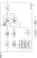
- FIG. 1 shows a first exemplary configuration of a circuit device of a present embodiment.
- a circuit device 100 includes an interface 110 (first interface), a pre-processing circuit 125, an image processing circuit 135, an interface 140 (second interface), a comparison circuit 145, a register circuit 170, and an interface 190 (third interface).
- the circuit device 100 is an integrated circuit device (IC), for example.
- the interface 110 receives image data that is transmitted from a processing device 200 or the like to the circuit device 100, and converts the received image data to a format that is used inside the circuit device 100, for example.
- the interface 110 is an OpenLDI (Open LVDS Display Interface), and converts a serial signal received using LVDS (Low Voltage Differential Signaling) to a RGB parallel signal.
- the processing device 200 is an SoC (System on a Chip), an MCU (Micro Control Unit), a CPU (Central Processing Unit), and the like.
- the pre-processing circuit 125 performs pre-processing on image data input from the interface 110, and outputs an image IMA1 subjected to the pre-processing. For example, the pre-processing circuit 125 performs gamma correction, FRC (Frame Rate Control), white balance processing, and the like, as the pre-processing.
- the pre-processing circuit 125 is a circuit that acquires an image input to the image processing circuit 135, and is also referred to as an image acquisition circuit.
- the image processing circuit 135 includes a mapping processing unit WEA1 that maps an image so as to conform to the surface shape of a projection target object, and a mapping processing unit WEA2 that performs reverse mapping thereof.
- the mapping processing unit WEA1 performs mapping processing on an image IMA1 that has been output from the pre-processing circuit 125 using map data MPA1, and outputs an image IMA2 subjected to the mapping processing.
- This mapping processing is processing for converting the image IMA1 such that the image projected on a projection target object is not distorted when viewed by a user.
- the mapping processing unit WEA2 performs mapping processing on the image IMA2 that has been output from the mapping processing unit WEA1 using map data MPA2, and outputs an image IMA3 subjected to the mapping processing.
- This mapping processing corresponds to a reverse conversion of the mapping processing performed by the mapping processing unit WEA1. That is, the mapping processing is to convert the image IMA2 that has been converted according to the projection target object to an image before conversion.
- the degree of matching between images IMA3 and IMA1 is high, and therefore, as a result of comparing the images IAM3 and IMA1 using a later-described comparison circuit 145, whether or not the image IMA2, which is the display image, is a normal image can be detected.
- the images IMA3 and IMA1 need not be completely matched with respect to image data, and the images need only be similar to a degree such that the images can be compared by the comparison circuit 145. That is, the mapping processing performed by the mapping processing unit WEA2 is a reverse conversion of the mapping processing performed by the mapping processing unit WEA1, but the reverse conversion need not be a reverse conversion so as to make the images IMA3 and IMA1 to completely match.
- the projection target object refers to an object on which the image IAM2 is projected or displayed. That is, the image IMA2 is output from the interface 140 to a projection device, and the projection device projects the image IMA2 on the projection target object.
- the image projected on the projection target object is displayed to the user.
- the projection device includes a liquid-crystal display panel, a display driver that drives the liquid-crystal display panel, a light source, and a lens, for example.
- the display driver causes the liquid-crystal display panel to display an image based on the image data, the light source outputs light to the liquid-crystal display panel, and the light that has passed through the liquid-crystal display panel is projected on the projection target object by the lens.
- the projection target object has a reflecting surface that reflects light projected thereon, and the reflecting surface is a surface of the projection target object, for example.
- the reflecting surface is a surface that reflects at least a portion of the incident light, and the reflection may be either of diffused reflection and specular reflection.
- the projection target object is a target object on which the head up display projects an image, and in the case of an in-vehicle head up display, the projection target object is an automobile windshield, or the like. Note that the projection target object is not limited to this example, and needs only be a target object on which an image is projected or displayed by a projection device.
- the mapping processing is processing in which coordinate conversion is performed with respect to pixel positions of an image based on map data.
- the mapping processing can include interpolation processing of pixel values or the like as processing that accompanies the coordinate conversion.
- the mapping processing includes forward mapping and reverse mapping. In the forward mapping, coordinates of pixel positions of an image before processing are converted to those of pixel positions of the image after processing, and the image after processing is generated using the result of the coordinate conversion. That is, pixels of the image before processing are successively selected, the coordinate of the pixel position (xa, ya) of a selected pixel is converted, and the pixel value of the pixel is set to the pixel value at the pixel position (ua, va) after coordinate conversion.
- the coordinates of pixel positions of the image after processing are converted to pixel positions of the image before processing, and an image after processing is generated using the result of coordinate conversion. That is, pixel positions of the image after processing are successively selected, the coordinate of a selected pixel position (ub, vb) is converted to a pixel position of the image before processing, and the pixel value of the pixel at the pixel position (xb, yb) is set to the pixel value at the pixel position (ub, vb) of an image after processing.
- the map data is data representing coordinate conversion associated with the shape of a reflecting surface of a projection target object, and is table data that associates the pixel positions of an image before mapping processing with the pixel positions of an image after mapping processing.
- the map used for the forward mapping is referred to as a forward map
- the map data is table data in which pixel positions (ua, va) of an image after mapping processing are associated with pixel positions (xa, ya) of an image before the mapping processing.
- the map used for the reverse mapping is referred to as a reverse map
- the map data is table data in which pixel positions (xb, yb) of an image before mapping processing are associated with pixel positions (ub, vb) of an image after the mapping processing.
- the map data MPA1 and MPA2 used by the mapping processing units WEA1 and WEA2 are input to the mapping processing units WEA1 and WEA2 from the processing device 200 via the interface 190, for example.
- the interface 140 outputs the image IMA2 to a device external to the circuit device 100.
- the device external to the circuit device 100 is a display driver that drives a display panel, for example.
- the interface 140 is an LVDS interface, and converts a RGB parallel signal from the image processing circuit 135 to an LVDS serial signal.
- the comparison circuit 145 performs processing for comparing the image IMA1 and the image IMA3, and outputs the comparison result.
- This comparison result is used to detect an error in the image IMA2. That is, the comparison result is used to verify whether or not the map data MPA1 is normal and the mapping processing has been properly performed by the mapping processing unit WEA1.
- the comparison circuit 145 obtains an index representing the degree of matching between the image IMA1 and the image IMA3. This index corresponds to a later-described shape index, and is an index whose value changes according to the degree of matching between the shapes or the edges of the shapes displayed in the images IMA1 and IMA3. Alternatively, a later-described visibility index may be obtained as the index.
- the visibility index is an index whose value changes according to the degree of dissimilarity between an image of a region of interest in which an icon or the like is displayed and an image of the other background region.
- the image in a region of interest is also referred to as a foreground image.
- the index indicating the contrast between a foreground image and a background image is obtained by comparing histograms of pixel values of the images IMA1 and IMA3.
- the register circuit 170 is configured to be accessible from the processing device 200 via the interface 190.
- the register circuit 170 includes a comparison result register 175 for storing comparison result information output from the comparison circuit 145, and the processing device 200 reads out the comparison result information from the comparison result register 175 via the interface 190.
- the processing device 200 includes an error detection circuit that performs error detection based on the comparison result information. An error in the image IMA2 to be projected onto a projection target object can be detected by the above-described image comparison and error detection. That is, whether or not the mapping processing performed by the mapping processing unit WEA1 has been properly performed is detected.
- comparison result information output by the comparison circuit 145 is stored in the register circuit 170, the processing device 200 reads out the comparison result information from the register circuit 170 via the interface 190, and the error detection circuit in the processing device 200 performs error detection, but there is no limitation thereto. That is, in the case where an error detection circuit is included in the circuit device 100 such as that shown in Fig. 4 or the like, the error detection circuit in the circuit device 100 may perform error detection based on the comparison result information output from the comparison circuit 145. In this case, after the error detection circuit in the circuit device 100 detected an error, the circuit device 100 may interrupt the processing device 200 so as to report the error.
- the interface 190 mediates communication between the circuit device 100 and processing device 200 with respect to setting information, control information, and the like.
- the interface 190 is a serial communication interface conforming to the SPI (Serial Peripheral Interface) method, the 12C method, or the like.
- SPI Serial Peripheral Interface
- the setting information and control information from the processing device 200 is written into the register circuit 170, for example, and the circuit device 100 performs an operation according to the setting information and control information.
- logic circuits included in the circuit device 100 may be configured as separate circuits, or may be configured as an integrated circuit using automatic placement and routing or the like, for example.
- the logic circuits are the pre-processing circuit 125, the image processing circuit 135, a comparison circuit 145, for example.
- a portion or all of the logic circuits may be realized by a processor such as a DSP (Digital Signal Processor).
- DSP Digital Signal Processor
- programs or instruction sets in which functions of the circuits are described are stored in a memory, and the functions of the circuits are realized by the processor executing the programs or the instruction sets.
- the pre-processing circuit 125 has been described as a circuit for acquiring an image to be input to the image processing circuit 135, but there is no limitation thereto.
- Fig. 2 shows a modification of the circuit device of the first exemplary configuration.
- the image data input from the interface 110 is denoted as IMA1'
- the mapping processing unit WEA1 performs mapping processing on the IMA1' using the map data MPA1.
- the configuration may be such that, thereafter, the post-processing circuit 126 performs gamma correction, FRC, white balance processing or the like on the image data subjected to mapping processing performed by the mapping processing unit WEA1 as post-processing.
- the post-processing circuit 126 corresponds to the pre-processing circuit 125 in Fig. 1 .
- the mapping processing unit WEA2 performs mapping processing on image data IMA2' output from the post-processing circuit 126 using the map data MPA2. In this case, in addition to confirming whether or not the mapping processing is properly performed, it can be confirmed whether the image has not been largely changed due to post-processing such as gamma correction, FRC, or white balance processing.
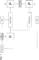
- FIG. 3 is a diagram schematically illustrating operations of the circuit device 100 in Fig. 1 .
- a map A is generated by performing map conversion processing on reference map data, and the reference map data is used as a map B.
- the nonvolatile memory 210 shown in Fig. 1 stores the reference map data
- the processing device 200 reads out the reference map data from the nonvolatile memory 210, and performs map conversion processing on the reference map data so as to generate the map data MPA1 associated with the map A.
- the map data MPA1 is input to the mapping processing unit WEA1 via the interface 190.
- the map conversion processing is conversion between the forward map and the reverse map, rotation of the map, parallel translation of the map, or the like.
- the processing device 200 outputs the reference map data as the map data MPA2 associated with the map B.
- the map data MPA2 is input to the mapping processing unit WEA2 via the interface 190.
- the warp engine A corresponds to the mapping processing unit WEA1, and performs mapping processing on the image IMA1 using the map A so as to generate the image IMA2.
- the mapping processing is also referred to as a warp processing.
- the warp engine B corresponds to the mapping processing unit WEA2, and performs reverse mapping processing on the image IMA2 using the map B so as to generate the image IMA3.
- This reverse mapping processing may include rotational transformation and parallel translation of an image corresponding to reverse conversion of the rotation and the parallel translation of the map in the map conversion processing.
- the warp engine A generates the image IMA2 for display, and therefore, performs high quality mapping processing relative to the warp engine B. For example, high-resolution mapping processing that adapts to the display resolution is performed. Also, interpolation processing of pixel values is performed in order to secure the display quality.
- the warp engine B generates the image IMA3 for error detection, and therefore, performs simplified mapping processing relative to the warp engine A. For example, as a result of thinning the pixels that are the target of the coordinate conversion, a low resolution image IMA3 relative to the image IMA1 is generated. Also, the interpolation processing of the pixel values may be omitted.
- thinning processing is performed on the image IMA1, as will be described later, positioning of the pixels in the images IMA1 and IMA3 is performed, and an index is obtained from the images subjected to the positioning.
- the map A is generated by performing map conversion processing on the reference map data. Therefore, when an abnormality occurs in the map A due to an error in the map conversion processing, it is possible that an abnormality will occur in the image IMA2 generated by the warp engine A using the map A. Also, even if there is no abnormality in the map A, when an abnormality occurs in the mapping processing performed by the warp engine A, it is possible that an abnormality will occur in the image IMA2 generated by the warp engine A. In order to detect such an abnormality, an error needs to be detected in an image deformed by the warp engine A, and it is difficult to perform error detection using a known technology.
- the CRC value of an image before conversion that is to be performed thereon by the warp engine A is used as the reference, and therefore the CRC value does not match, in principle, the CRC value obtained from the image subjected to the conversion performed by the warp engine A.
- reverse mapping processing is performed on the image IMA2 by the warp engine B, and the image IMA3 subjected to the reverse mapping processing and the original image IMA1 are compared so as to obtain an index representing the degree of matching.
- the degree of matching between the images IMA3 and IMA1 is high, and therefore an error in the image IMA2 can be detected using the index.
- the index has a value that changes according to the degree of matching, and therefore the images IMA1 and IMA3 need not be completely matched.
- the error is to a degree such that the image IMA2 can be visually recognized by a user, no-error may be determined.
- the index is judged using a threshold value in the error detection, and as a result of setting the threshold value, the degree of matching at which an error is determined can be adjusted.
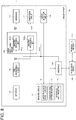
- Fig. 4 shows a second exemplary configuration of the circuit device of the present embodiment.
- the circuit device 100 includes the error detection circuit 150.
- the register circuit 170 includes an error detection result register 176, an operation mode setting register 177, and a threshold value register 178. Note that the constituent elements that are the same as the constituent elements that have already been described will be denoted by the same reference signs, and the description thereof will be omitted, as appropriate.
- the comparison circuit 145 outputs a result of comparison between the images IMA1 and IMA3 to the error detection circuit 150.
- the error detection circuit 150 performs error detection on the image IMA2 for display based on the comparison result.
- the comparison result is the index described above
- the error detection circuit 150 performs the error detection by comparing the index with a threshold value.
- the threshold value with respect to the shape index is a threshold value that indicates an allowable similarity.
- the threshold value with respect to the visibility index is a threshold value that indicates allowable visibility.
- the image processing circuit 135 stops outputting an image IMA2 to the interface 140.
- the interface 140 stops outputting an image IMA2.
- the interface 140 outputs an image IMA2 along with error information, and the display driver that has received the error information may perform an operation based on the error information.
- the error information is an error determination flag, an index, or the like, for example.
- the operation based on the error information is stopping display or the like, for example.
- the error detection result register 176 stores an error detection result output from the error detection circuit 150.
- the error detection result is an error determination flag that indicates whether or not an error has been determined with respect to a display image, for example.
- Mode setting information is set into the operation mode setting register 177 from the processing device 200 via the interface 190.
- the mode setting information is information regarding the operation mode to be set in the circuit device 100 when the error detection result indicates an error, and is information regarding the operation to be performed when an error is detected.
- the image processing circuit 135 performs the operation that is to be performed at the time when an error is detected based on the mode setting information. Note that the configuration may be such that the operation that is to be performed at the time when an error is detected is performed by the processing device 200. In this case, the processing device 200 reads out the error detection result from the error detection result register 176 via the interface 190. The processing device 200 performs the operation that is to be performed at the time when an error is detected if the error detection result indicates an error.
- the operation that is to be performed at the time when an error is detected is to stop transmitting image data to the circuit device 100, to transmit predetermined image data to the circuit device 100, or the like, for example.
- the predetermined image data is image data of an image to be displayed to a user when an error is detected.
- a threshold value is set into the threshold value register 178 from the processing device 200 via the interface 190.
- the error detection circuit 150 performs error detection by comparing the index and the threshold value set into the threshold value register 178. That is, the error detection circuit 150 compares the shape index with a shape index threshold value, compares the visibility index with a visibility index threshold value, performs error detection based on the comparison results, and outputs the result as the error detection result. For example, if at least one of the comparison results indicates an error, it is determined that the second image includes an error.
- the configuration may be such that the circuit device 100 does not output the error detection result to a device external to the circuit device 100, and may use the error detection result only inside the circuit device 100.
- the circuit device 100 may shift to a safe mode. In the safe mode, control such that a predetermined error notification image is transmitted to a display driver, or a backlight of a liquid-crystal display device is turned off, for example, may be performed. Accordingly, an error state can be directly reported to a user not by the control from the processing device 200, but by the control from the circuit device 100.
- a head up display controller that controls a head up display or a display controller that controls a display driver can be envisioned as the circuit device 100 in Fig. 1 or 4 described above.
- the circuit device to which the method of the present embodiment can be applied is not limited thereto.
- the circuit device may be a display driver that includes a function of the display controller.
- the circuit device is an integrated circuit device (IC), for example.
- the circuit device may include a plurality of integrated circuit devices.
- the circuit device includes a head up display controller, which is a first integrated circuit device, and a processing device, which is a second integrated circuit device.
- the head up display controller includes a comparison circuit that performs processing of comparing between the images IMA1 and IMA3
- the processing device includes an error detection circuit that performs error detection based on a result of comparison received from the head up display controller.
- Fig. 5 shows a detailed exemplary configuration of the comparison circuit 145.
- the comparison circuit 145 includes a pixel arrangement processing unit 146 and an index acquisition unit 147.
- the pixel arrangement processing unit 146 performs pixel arrangement processing for performing comparison between the images IMA1 and IMA3, and outputs the images IMA1 and IMA3 subjected to the processing to the index acquisition unit 147. Since the resolution of the image IMA3 is lower than that of the image IMA1, as described above, the comparison circuit 145 reduces the resolution of the image IMA1 so as to match the resolution of the image IMA3, and compares the image IMA3 with the image IMA1 whose resolution has been reduced. For example, the pixel arrangement processing unit 146 performs subsampling processing on the image IMA1 such that the number of pixels of the image IMA1 matches the number of pixels of the image IMA3. Also, rotation processing, translational processing, interpolation processing, and the like may be performed such that corresponding pixels of the images IMA1 and IMA3 are arranged at the same pixel positions.
- the index acquisition unit 147 obtains an index for detecting an error in the image IMA2 based on the images IMA1 and IMA3 subjected to the pixel arrangement processing.
- the index is a shape index, and a visibility index may further be acquired. The details of the shape index and the visibility index will be described later.
- the index output from the index acquisition unit 147 is stored in the comparison result register 175 as information regarding the comparison result.
- the error detection circuit 150 performs error detection based on the index.
- the image processing circuit 135 performs first mapping processing, which is processing of mapping an input first image to a second image to be projected onto a projection target object, and second mapping processing for converting the second image to a third image, which is reverse mapping processing of the first mapping processing.
- the comparison circuit 145 performs comparison between the first image and the third image, and outputs the result of comparison as information for performing error detection on the second image.
- IMA1 indicates the first image
- IMA2 indicates the second image
- IMA3 indicates the third image
- the mapping processing performed by the mapping processing unit WEA1 is the first mapping processing
- the mapping processing performed by the mapping processing unit WEA2 is the second mapping processing.
- the information for performing the error detection is information regarding the result of comparison between the images IMA1 and IMA3, and corresponds to the later-described shape index or visibility index, or the shape index and the visibility index, for example.
- the mapping processing or the map data when an abnormality occurs in the mapping processing or the map data, an abnormality occurs in the second image, but it is difficult to detect the abnormality using a known technique.
- the first image and the third image can be compared. Since the third image is generated from the second image, it can be determined that there is no error in the second image, if the degree of matching between the third image and the first image, which is the reference, is high. In this way, whether the image to be projected onto a projection target object such as a head up display, for example, has appropriate display content can be detected.
- the comparison circuit 145 obtains an index representing the degree of matching between the first image and the third image, as the result of comparison, based on the pixel values of the first image and the pixel values of the third image, or based on the pixel values of an edge image of the first image and the pixel values of an edge image of the third image.
- the pixel value of an edge image indicates an edge amount of the corresponding pixel, and is a signal value obtained by performing edge extraction.
- the index representing the degree of matching is the shape index, and the details thereof will be described later.
- an error in the third image can be detected based on the index representing the degree of matching between the first image and the third image without performing bit-wise error detection such as CRC. If an error is not detected in the third image, it can be determined that the mapping processing has been properly performed, and therefore, an error in the second image that is generated through mapping processing can be detected.
- an icon and the like to be presented to a user are displayed in an in-vehicle head up display or the like. According to the present embodiment, such an icon can be displayed to the user as long as the shape thereof can be properly recognized, without stopping display due to one-bit error or the like.
- the image processing circuit 135 performs the first mapping processing using first map data generated from map data associated with the projection target object, and performs the second mapping processing using second map data, which is the map data.
- the map data associated with the projection target object is map data stored in the nonvolatile memory 210.
- the first map data is the map data MPA1, and is the data of the map A generated through the map conversion processing.
- the second map data is the map data MPA2, and data of the map B, which is map data read out from the nonvolatile memory 210.
- the third image which is an image used for comparison, is generated using reference map data as the second map data as is. Accordingly, as a result of performing comparison between the third image and first image, whether or not the first mapping processing using the first map data has been properly performed can be determined.
- the circuit device 100 includes the error detection circuit 150 that performs error detection on the second image based on the result of comparison performed by the comparison circuit 145.
- the error detection circuit 150 incorporated in the circuit device 100 can perform error detection on the display image. Also, the circuit device 100 can perform an operation that is to be performed at the time when an error has been detected based on the error detection result. Alternatively, the error detection result is output to the processing device 200 and the like, and the processing device 200 and the like can perform an operation that is to be performed at the time when an error has been detected based on the error detection result.
- the circuit device 100 includes the operation mode setting register 177 in which the operation mode of the circuit device 100 when an error is determined by the error detection circuit 150 is set.
- the operation mode of the circuit device 100 when an error is determined in the second image based on the result of comparison between the first image and the second image can be set into the operation mode setting register 177 via an interface.
- the processing device 200 can set an operation mode in the operation mode setting register 177 via the interface 190.
- the circuit device 100 can be caused to perform an operation desired by a user at the time when an error is detected, for example.
- a mode of reporting the result of error detection to an external device external to the circuit device 100, a mode of the second image being not displayed, and a mode of displaying a specific image are set as operation modes in the operation mode setting register 177.
- the external device is the processing device 200, for example, which is an SoC, a CPU, or the like.
- the result of error detection is output to the external device via the interface 190, for example.
- the circuit device 100 cannot transmit a notification to the processing device 200.
- the circuit device 100 interrupts the processing device 200 to perform notification, and the processing device can read out detailed information from the circuit device via the interface.
- An image being not displayed is to set the display panel to a state in which an image is not displayed, and is to cause the display panel to display black or white over the entire display region, for example.
- the specific image is an image that is different from the display image, which is the target of the error detection, and is an image desired to be displayed when an error is detected.
- the specific image is an image in which a message, a symbol, a color, or the like that is desired to be presented to the user when an error is detected is displayed, for example.
- a predetermined color such as red is displayed in the entirety of or a portion of the display region of the display panel, for example.
- the operation mode of the circuit device 100 when an error has been determined in the second image can be set to one of the above-described three modes.
- the circuit device 100 can be caused to perform one of the above-described three modes, as the operation desired by the user when an error is detected.
- the error detection circuit 150 performs error detection by comparing the result of comparison with a threshold value for determining an error in the second image.
- the threshold value for determining an error in the second image is a threshold value to be compared with the index, which is the comparison result.
- the index which is the result of comparison, in the present embodiment is not only an index that simply indicates whether or not there is an error, but is also an index whose value changes according to the degree of matching between the first image and the third image.
- error detection can be performed even in a case where a data error detection method such as CRC cannot be used. That is, an error can be determined when it is determined that the similarity of the shapes cannot be secured based on the degree of matching.
- the circuit device 100 includes the threshold value register 178 in which threshold values are set.
- a threshold value to be compared with an index which is the result of comparison, can be set into the threshold value register 178 via an interface.
- the processing device 200 can set a threshold value to the threshold value register 178 via the interface 190.
- the threshold value such that the value thereof can be changed
- the degree of similarity between shapes at which an error is determined can be changed.
- a user can freely set the threshold value, which is an error determination criterion, for example.
- Fig. 6 shows a third exemplary configuration of the circuit device of the present embodiment.
- the image processing circuit 135 includes a mapping processing unit WEB1 that maps an image so as to conform to the surface shape of a projection target object, and a mapping processing unit WEB2 that performs mapping in the same direction.
- the comparison circuit 145 compares images IMB2 and IMB3 that are respectively output from the mapping processing units WEB1 and WEB2. Note that the constituent elements that are the same as the constituent elements that have already been described will be denoted by the same reference signs, and the description thereof will be omitted, as appropriate.
- the pre-processing circuit 125 outputs an image IMB1 subjected to pre-processing.
- the content of the pre-processing is similar to the content described in Fig. 1 .
- the mapping processing unit WEB1 performs mapping processing on the image IMB1 output from the pre-processing circuit 125 using map data MPB1, and outputs the image IMB2 subjected to the mapping processing.
- This mapping processing is similar to the mapping processing performed by the mapping processing unit WEA1 in Fig. 1 .
- the mapping processing unit WEB2 performs mapping processing on the image IMB1 output from the pre-processing circuit 125 using map data MPB2, and outputs the image IMB3 subjected to the mapping processing.
- This mapping processing is processing of mapping an image so as to conform to the surface shape of the projection target object, but need not be the same as the mapping processing performed by the mapping processing unit WEB1. That is, at least one of the map data and the mapping processing may be different from those of the mapping processing unit WEB1.
- the mapping processing unit WEB2 generates a low resolution image IMB3 relative to the image IMB2.
- the interpolation processing of the pixel values may be omitted.
- the comparison circuit 145 performs processing of comparing between the image IMB2 and the image IMB3, and outputs the result of comparison. This result of comparison is used for detecting an error in the image IMB2. That is, the result of comparison is used for verifying whether or not the map data MPB1 is normal and the mapping processing has been properly performed by the mapping processing unit WEB1. Specifically, the comparison circuit 145 obtains an index that represents the degree of matching between the image IMB2 and the image IMB3. This index corresponds to the later-described shape index. Alternatively, the later-described visibility index may be obtained as the index.
- the register circuit 170 includes the comparison result register 175 for storing comparison result information output from the comparison circuit 145.
- the processing device 200 performs error detection based on comparison result information read out from the comparison result register 175 via the interface 190.
- the error detection performed on the image IMB2 to be projected onto a projection target object is realized by the above-described image comparison and error detection. That is, whether or not the mapping processing has been properly performed by the mapping processing unit WEB1 is detected.
- FIG. 7 is a diagram schematically illustrating the operations of the circuit device 100 in Fig. 6 .
- map conversion processing is performed on reference map data so as to generate a map C, and the reference map data is used as a map D.
- the nonvolatile memory 210 shown in Fig. 6 stores the reference map data
- the processing device 200 reads out the reference map data from the nonvolatile memory 210, performs map conversion processing on the reference map data so as to generate map data MPB1 associated with the map C.
- the map data MPB1 is input to the mapping processing unit WEB1 via the interface 190.
- the processing device 200 outputs the reference map data as map data MPB2 associated with the map D.
- the map data MPB2 is input to the mapping processing unit WEB2 via the interface 190.
- the warp engine C corresponds to the mapping processing unit WEB1, and performs mapping processing on the image IMB1 using the map C so as to generate the image IMB2.
- the warp engine D corresponds to the mapping processing unit WEB2, and performs mapping processing on the image IMB1 using the map D so as to generate the image IMB3.
- This mapping processing may include rotational transformation and parallel translation of an image corresponding to the rotation and parallel translation of a map in the map conversion processing.
- the warp engine C generates the image IMB2 for display, and therefore, performs high quality mapping processing relative to the warp engine D. For example, high-resolution mapping processing that adapts to the display resolution is performed. Also, interpolation processing of pixel values is performed in order to secure the display quality.
- the warp engine D generates the image IMB3 for error detection, and therefore, performs simplified mapping processing relative to the warp engine C. For example, as a result of thinning the pixels that are the target of the coordinate conversion, a low resolution image IMB3 relative to the image IMB2 is generated. Also, the interpolation processing of the pixel values may be omitted.
- comparison processing performed by the comparison circuit 145, thinning processing is performed on the image IMB2, positioning of the pixels in the images IMB2 and IMB3 is performed, and an index is obtained from the images subjected to the positioning.
- the detailed configuration of the comparison circuit 145 is similar to that shown in Fig. 5 . That is, IMA1 and IMA3 in Fig. 5 need only be replaced by IMB2 and IMB3.
- the warp engine D performs mapping processing in the same direction as the warp engine C, compares the images IMB2 and IMB3 that have been subjected to the mapping processing so as to obtain an index representing the degree of matching.
- the degree of matching between the images IMB2 and IMB3 is high, and therefore an error in the image IMB2 can be detected using the index.
- the index has a value that changes according to the degree of matching, and therefore the images IMB2 and IMB3 need not be completely matched. That is, even if there is a minute abnormality in the map C or the warp engine C, if the error is to a degree such that the image IMB2 can be visually recognized by a user, no-error may be determined.
- Fig. 8 shows a fourth exemplary configuration of the circuit device of the present embodiment.
- the circuit device 100 includes the error detection circuit 150.
- the register circuit 170 includes the error detection result register 176, the operation mode setting register 177, and the threshold value register 178. Note that the constituent elements that are the same as the constituent elements that have already been described will be denoted by the same reference signs, and the description thereof will be omitted, as appropriate.
- the comparison circuit 145 outputs the result of comparison between the images IMB2 and IMB3 to the error detection circuit 150.
- the error detection circuit 150 performs error detection on the image IMB2 for display based on the result of comparison. In the case where the result of comparison is the above-described index, the error detection circuit 150 performs the error detection by comparing the index with a threshold value.
- the configuration may be such that the circuit device 100 does not output the error detection result to a device external to the circuit device 100, and may use the error detection result only inside the circuit device 100.
- a head up display controller that controls a head up display and a display controller that controls a display driver are envisioned as the circuit device 100 in Fig. 6 or 8 .
- the circuit device to which the present embodiment can be applied is not limited thereto.
- the circuit device may be a display driver that includes a function of the display controller.
- the circuit device is an integrated circuit device (IC), for example.
- the circuit device may include a plurality of integrated circuit devices.
- the circuit device includes a head up display controller, which is a first integrated circuit device, and a processing device, which is a second integrated circuit device.
- the head up display controller includes a comparison circuit that performs processing of comparing between the images IMB2 and IMB3, and the processing device includes an error detection circuit that performs error detection based on the result of comparison received from the head up display controller.
- the image processing circuit 135 performs the first mapping processing, which is processing of mapping an input first image on a second image to be projected onto a projection target object, based on map data associated with the projection target object, and the second mapping processing in which the first image is converted to a third image by the second mapping processing that is different from the first mapping processing.
- the comparison circuit 145 performs comparison between the second image and the third image, and outputs the result of comparison as information for performing error detection on the second image.
- IMB1 indicates the first image
- IMB2 indicates the second image
- IMB3 indicates the third image
- the mapping processing performed by the mapping processing unit WEB1 is the first mapping processing
- the mapping processing performed by the mapping processing unit WEB2 is the second mapping processing.
- the information for performing the error detection is the information regarding the result of comparison between the images IMB2 and IMB3, and corresponds to the later-described shape index or visibility index, or the shape index and the visibility index, for example.
- the first and second mapping processing being different means that the hardware or the algorithm is different therebetween.
- the mapping processing units WEB1 and WEB2 may be constituted by separate mapping processing circuits.
- the first and second mapping processing being different means that at least one of the map data and the content of the mapping processing is different therebetween.
- the map C used by the warp engine C that handles the first mapping processing is obtained by performing map conversion processing on the reference map data
- the map D used by the warp engine D that handles the second mapping processing may be the reference map data itself.
- the first mapping processing is one of forward mapping and reverse mapping
- the second mapping processing is the other thereof.
- the first and second mapping processing may be mapping processing having different resolution.
- the first mapping processing may include interpolation processing, and the second mapping processing may not include interpolation processing.
- the first image is converted to the second and third images by being respectively subjected to the first mapping processing and second mapping processing.
- the first mapping processing and second mapping processing are each mapping processing in the same direction that performs similar deformation on the first image. Accordingly, the second image and the third image can be compared. If the degree of matching between the second image and the third image is high, it can be determined that there is no error in the second image. In this way, it can be detected whether the image to be projected onto a projection target object such as a head up display has appropriate display content, for example. Also, since the second mapping processing is mapping processing that is different from the first mapping processing, the occurrence of the same abnormality both in the first mapping processing and second mapping processing can be avoided, and error detection accuracy can be improved.
- the comparison circuit 145 obtains an index representing the degree of matching between the second image and the third image, as the result of comparison, based on the pixel values of the second image and the pixel values of the third image, or based on the pixel values of an edge image of the second image and the pixel values of an edge image of the third image.
- an error in the second image can be detected based on the index representing the degree of matching between the second image and the third image without performing bit-wise error detection such as CRC. If an error is not detected in this processing, it can be determined that the mapping processing has been properly performed, and therefore, an error in the second image that is generated through mapping processing can be detected.
- an icon and the like to be presented to a user are displayed in an in-vehicle head up display or the like. According to the present embodiment, such an icon can be displayed to the user as long as the shape thereof can be properly recognized, without stopping display due to one-bit error or the like.
- the image processing circuit 135 performs the first mapping processing using the first map data generated from map data that is associated with the projection target object, and performs the second mapping processing using the second map data, which is the map data.
- the map data associated with the projection target object is map data stored in the nonvolatile memory 210.
- the first map data is the map data MPB1, and is the data of map C generated by performing map conversion processing.
- the second map data is the map data MPB2, and is the data of map D, which is map data read out from the nonvolatile memory 210.
- the reference map data is used as the second map data as is, and the third image used for comparison is generated. Accordingly, it can be determined whether or not the first mapping processing using the first map data has been properly performed based on the result of comparison between the third image and the second image.
- the image processing circuit 135 generates the third image whose resolution is low relative to the first image and the second image.
- the comparison circuit 145 reduces the resolution of the second image so as to match the resolution of the third image, and compares the second image subjected to the resolution reduction with the third image.
- the pixel arrangement processing unit 146 reduces the resolution of the second image so as to match the resolution of the third image, and the index acquisition unit 147 obtains the index by comparing the second image subjected to the resolution reduction with the third image.
- low resolution mapping processing can be adopted as the second mapping processing for generating the third image. Accordingly, the processing load of the second mapping processing can be reduced, or the circuit scale of the hardware that performs the second mapping processing can be reduced. Also, as a result of reducing the resolution of the second image so as to match the resolution of the third image, the second image can be compared with the third image.
- comparison processing performed by the comparison circuit 145 and the error detection processing performed by the error detection circuit 150 will be described. Note that a case where an index is acquired in the comparison processing will be described as an example, and the comparison processing is referred to as index acquisition processing. Note that the comparison processing is not limited thereto, and various types of image comparison can be used.
- an image processing system in which content is displayed in a display, there are cases where whether or not a predetermined region in an image matches the initially intended region needs to be confirmed.
- a case where an important image is displayed in a cluster display of an automobile system is considered.
- the cluster display is a meter panel display.
- a predetermined piece of important information needs to be displayed via a visible image overlaid on existing content displayed in a screen.
- various methods for detecting whether or not an image is properly displayed will be described. The detection is performed by analyzing a region of interest, and deriving some important indices that indicate the degree of properness in displaying the region.
- the region of interest is the entirety of an image, but a partial region of an image may be the region of interest.
- ROI Region Of Interest
- an image to be the target of analysis is referred to as an analysis image
- an image to be a reference of the analysis is referred to as a reference image.
- the image IMA3 is the analysis image
- the image IMA1 is the reference image.
- the image IMB2 is the analysis image
- the image IMB3 is the reference image. Note that the comparison processing is relative comparison between two images, and therefore the analysis image and the reference image may be exchanged.
- the shape index is an index indicating whether or not the shapes of the analysis image and the reference image in a region of interest match.
- a computation method of the shape index will be described.
- Fig. 9 shows a first example of the analysis image.
- A1 indicates the region of interest
- A2 indicates an icon. Note that the broken line that shows the region of interest is not actually rendered in the display image. Also, here, the region of interest is a portion of the analysis image, but the region of interest may be the entirety of the analysis image.
- pixel blocks in the ROI of the analysis image are averaged such that the size of the ultimate averaged image is m ⁇ n pixels.
- This subsampling processing is performed such that a small number of pixel errors are not detected as an important error, and the entire shapes of the reference image and the analysis image are confirmed while ignoring these errors.
- the errors desired to be ignored are color shift, slight distortion, and the like.
- the resolution of the image obtained through subsampling can be increased.
- the value mxn can be selected according to the application. As will be described later, when used in relation to the reference image, the value mxn is selected based on sample data observation.
- the averaging block size is u/m ⁇ v/n pixels.
- reference background information cannot be used, pixels of a portion of the analysis image in which reference pixels do not exist are deleted. This operation corresponds to reference foreground masking. This is performed because it is necessary that the baseline with respect to background pixels is matched (aligned, put under the same condition) between the reference image and the analysis image.
- the baseline being matched means being aligned or being put under the same conditions. Therefore, the values of the background pixels are set to the same value both in the analysis image and the reference image.
- the reference image is also averaged so as to have a size of mxn pixels. Averaging is performed separately on each of the channels.
- Fig. 10 shows an example of the reference image.
- a foreground F1 which is an icon of a reference image RIA is colored, and a background, which is a region other than the icon, is not colored, that is black, for example.
- the size of the reference image RIA is 256 ⁇ 256 pixels.
- the background of a region of interest of the analysis image may be made colorless, and an averaged image of the image of the region of interest may be obtained.
- the background may be made colorless by deleting the background.
- the averaged image (SRef m ⁇ n) of the reference image and the averaged image (SAnz m ⁇ n) of the region of interest of the analysis image are compared pixel by pixel using a distance reference, and a distance D is obtained using Equation (1).
- the distance D is a three-dimensional distance.
- the distance reference is a square of Cartesian distance, but a similar parameter can be obtained with another distance reference.
- R xyc ⁇ R c ′ ⁇ A xyc ⁇ A c ′ 2 c represents the channel
- x represents the pixel position in the averaged image in a lateral direction
- y represents the pixel position in the averaged image in a longitudinal direction.
- the lateral direction is also referred to as a horizontal direction
- the longitudinal direction is also referred to as a vertical direction.
- m and n represent the size of the averaged image.
- R xyc represents the pixel value at a position (x, y) in the averaged image of the reference image in the channel c.
- R' c represents an average value of R xy pixels in the channel c.
- the average value of the R xy pixels is obtained by averaging the R xyc values inside the averaged image.
- a xyc represents the pixel value at a position (x, y) in the averaged image of the analysis image in the channel c.
- A' c represents an average value of A xy pixels in the channel c.
- the average value of the A xy pixels is obtained by averaging the A xyc inside the averaged image.
- the average value is subtracted in each channel is to make a small color shift between the reference image and the analysis image to not be treated as an error.
- the average value can be set to 0. In this case, matching of the shape and color is checked using the distance reference.
- the shape index S is derived from the distance parameter using the following Equations (2) and (3).
- the shape index S is also referred to as a shape parameter.
- the function f is selected so as to be easily implemented by hardware.
- the function f may be a scaling function K that scales a range from 0 to 1 to a range from 0 to k, for example.
- the shape index S represents the degree of matching of the shape between the reference image and the analysis image. When the images do not match, this value decreases, and has tendency to become 0. This example will be described in the following.
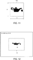
- Fig. 9 the icon, which is the reference image, is properly displayed in the analysis image.
- Fig. 12 shows a second example of the analysis image.
- B1 indicates the region of interest.
- the icon which is the reference image, is not clear in the analysis image. That is, some of the reference pixels do not exist in the analysis image, and if the function f is a unit function, the shape index S takes a value of less than one. In the case of such an unclear foreground, the shape index takes a small value. Note that the later-described visibility index also takes a small value.
- Fig. 13 is a third example of the analysis image.
- E1 indicates the region of interest.
- the icon, which is the reference image is rotated in the analysis image.
- the shape index S takes a value of less than one.
- the shape index takes a small value.
- the later-described visibility index takes a large value.
- the above-described shape index only checks matching in the base signal.
- parameters can be obtained using a shape computation algorithm.
- the edge detection kernel is Laplacian, Sobel, or the like, for example. Using the obtained parameters, an error in detection that has occurred based on the shape index can be excluded. In this way, even in a case of an image having low visibility, a proper error detection result can be obtained.
- Fig. 14 shows a fourth example of the analysis image.
- an icon ICA is overlaid on a dashboard image DIM.
- the icon image is blended with the dashboard image at some transmission factor.
- edges in the analysis image and the reference image in a region of interest are detected using an edge detection technique.
- the edge detection technique is an edge detection technique using a Sobel edge detection convolution operator, for example.
- Fig. 15 shows an example of the analysis image in a region of interest.
- the display image CIB is an image of the region of interest in which the reference image ICB is blended into the dashboard image DIM.
- the dashboard image DIM can be seen through the icon in the icon portion. Note that, if there is no error, the reference image in the region of interest is expected to be an image similar to that in Fig. 15 .
- Fig. 16 is an example of edge values calculated from an analysis image.
- ECIB indicates an edge image of the image CIB in Fig. 15 .
- edges are shown by black lines and grey lines, but the strength of an edge can be shown in grey scale in actuality.
- a white portion indicates an edge at high intensity, and a black portion indicates no edge.
- This edge detection is performed on a luminance channel.
- the edge detection is performed on a color channel or in a color space such as YCbCr as well. Note that, if there is no error, the edge image of the reference image in the region of interest is expected to be an image similar to that in Fig. 16 .
- Edges in the foreground region and a background region are calculated with respect to the reference image and the analysis image, and the shape index is calculated by calculating a similarity amount as shown in the following Equations (4) to (15).
- Match in the following Equation (15) is the shape index.
- the shape index is also referred to as a conformity value. In the following, it is assumed that the reference image has a size of m ⁇ n pixels, and the region of interest of the display image has the size of m ⁇ n pixels as well.
- Equation (4) is a horizontal Sobel kernel, which is a Sobel filter operator for detecting edges in a horizontal direction.
- Equation (5) is a vertical Sobel kernel, which is a Sobel filter operator for detecting edges in a vertical direction.
- F H 1 0 ⁇ 1 2 0 ⁇ 2 1 0 ⁇ 1
- F V 1 2 1 0 0 0 ⁇ 1 ⁇ 2 ⁇ 1
- an edge value is calculated at each pixel position in the reference image and the region of interest of the display image.
- "*" is a convolution operator.
- IRef is a luminance (Y) channel of the reference image.
- IRef (x,y) is a pixel at the position (x, y) in the luminance channel of the reference image.
- x is an integer that satisfies 0 ⁇ x ⁇ m
- y is an inter that satisfies 0 ⁇ y ⁇ n.
- IRen is a luminance channel of the display image in the region of interest.
- IRen (x,y) indicates 3 ⁇ 3 pixels that are centered at a position (x, y) in the luminance channel of the display image in the region of interest.
- E 1 x y E 1 H E 1 V x y N
- E 1 H x y F H ⁇ IRef x y
- E 1 V x y F V ⁇ IRef x y
- E 2 x y E 2 H E 2 V x y N
- E 2 H x y F H ⁇ IRen x y
- E 2 V x y F V ⁇ IRen x y
- the shape index Match (conformity value) is obtained from the above-described edge values.
- "•" represents an inner product operator.
- Match S T 1 + T 2 / 2
- Equation (16) to (21) are used.
- E 1 x y f E 1 x y M x y [Math. 17]
- E 2 x y f E 2 x y M x y [Math. 18]
- M (x,y) may be mask pixels that define on which pixels comparison is to be performed.
- This mask can be realized by a simple 1-bit mask in which a pixel that is not a comparison target is defined by 0, and a pixel that is a target of comparison is defined by 1. For example, in a case where image comparison is desired to be performed on a portion of the region of interest, such as a case where only an icon is the comparison target, a mask according to the desire may be set.
- the comparison circuit 145 obtains an index that represents the degree of matching between the analysis image and the reference image based on the pixel values of the analysis image and the pixel values of the reference image, or based on the pixel values of an edge image of the analysis image and the pixel values of an edge image of the reference image.
- the error detection circuit 150 performs error detection on the display image based on the index.
- error detection can be performed on an analysis image based on the index that represents the degree of matching between the analysis image and a reference image, without performing bit-wise error detection such as CRC.
- the degree of matching between the analysis image and the reference image is high, it is highly possible that the shape of the analysis image is visually seen as the same shape as the reference image. That is, according to the present method, it is possible that an error is determined when the shape of an analysis image is not properly displayed. Also, if an error is not detected in the analysis image, it can be determined that the mapping processing has been properly performed, and therefore, as a result of performing error detection on the analysis image, an error in an image to be projected onto a projection target object can be detected.
- the first computation method shown by the above Equations (2) to (4) corresponds to a case where the index (S) is obtained based on the pixel values of an analysis image and the pixel values of a reference image.
- the second computation method shown by the above Equations (5) to (21) corresponds to a case where the index (Match) is obtained based on the pixel values of an edge image of the analysis image and the pixel values of an edge image of the reference image.
- the pixel value of an edge image corresponds to an edge amount in the above Equations (6), (9), (16), and (17).
- the degree of matching refers to a matching degree of the shape of an icon, a character, a figure, a mark, or the like (hereinafter referred to as icon or the like), for example. More specifically, the degree of matching refers to a matching degree with respect to the outline and the orientation of an icon or the like. Also, furthermore, the degree of matching may include a matching degree of the state of the inside of the outline of an icon or the like, that is, the state as to whether or not the inside of an outline is filled or the like, for example. For example, the index representing the degree of matching has a larger value as the degree of matching between the foreground image and the background image increases.
- the comparison circuit 145 obtains the index (S) from a value obtained by dividing a given threshold value (T) by the distance information (D).
- the index (S) whose value increases as the matching degree of the shapes increases can be obtained by dividing the given threshold value by the distance information.
- the comparison circuit 145 performs a sum-of-product operation (Equation (12)) of the pixel values of an edge image of the analysis image and the pixel values of an edge image of the reference image, and obtains the index from the result of the sum-of-product operation (Equation (15)).
- the edge image is an image in which the pixel value of each pixel represents an edge amount.
- the edge image of the analysis image is compared with the edge image of the reference image with respect to the same pixel, the edge amounts must be the same (approximately the same).
- the positions of edges are different between the analysis image and the reference image, therefore, even if there is a large edge amount in the edge image of the analysis image, there are cases where the edge amount of the same pixel in the edge image of the reference image is zero, for example.
- the "product" of the sum of products is an inner product of vectors, but the “product” is not limited thereto.
- the edge amount is defined by a scalar
- the “product” is a product of scalars.
- the terms of analysis image and reference image are used similarly to the computation of the shape index.
- the image IMA3 is the analysis image
- the image IMA1 is the reference image.
- the image IMB2 is the analysis image
- the image IMB3 is the reference image. Note that the comparison processing is relative comparison between two images, and therefore the analysis image and the reference image may be exchanged.
- Fig. 17 shows a histogram of YCbCr channels in a region of interest. Also, Fig. 18 shows cross-correlation values obtained by performing a cross-correlation operation on the histograms of the analysis image and the reference image.
- a histogram is obtained for each channel of a YCbCr image using n binaries. For example, 256 binaries are used, and a histogram that includes a set of different binaries can be generated.
- the histogram is generated by counting the number of occurrences of a specific value in a region of interest. That is, for each of the channels of a YCbCr image, the number of pixels that have a value indicated by each binary is counted in the region of interest.
- the histogram is normalized to have a value from 0 to a.
- a cross-correlation operation is performed on the histograms of the analysis image and the reference image for each channel. Then, the resultant cross-correlation signal is used in an analysis thereafter. As shown in Fig. 18 , the cross-correlation signal is normalized such that the peak value at zero delay is one or a pre-set value.
- the cross-correlation value can be obtained using the following Equation (22).
- f and g represent functions on which the correlation operation is performed.
- One of the functions f and g is the histogram of the analysis image, and the other of the functions f and g is the histogram of the reference image.
- f*g represents the correlation operation between the function f and the function g.
- m represents binary number in the histogram.
- n represents a delay (lag), and n is an integer from -255 to +255, in Fig. 18 .
- 256 binaries are normalized to values from 0 to 1 in the histogram in Fig. 17 , and therefore the horizontal axis shows a value from 0 to 1.
- the correlation values in Fig. 18 are obtained by changing the delay by one binary, and therefore the horizontal axis shows values from -(256-1) to +(256-1).
- Fig. 18 when a two-color image exists in the region of interest, sidebands are obtained through the correlation operation.
- the distance of the delay from the center at which the above-described peak occurs indicates the contrast between colors.
- the center corresponds to zero delay. Because the human eye can distinguish features of an image through a contrast, the peaks of all of the three channels need to be checked.
- the contrast is a luminance contrast or color contrast, for example.
- the Y channel is indicated by broken lines
- the Cb channel is indicated by thin solid lines
- the Cr channel is indicated by thick solid lines.
- the checking is performed by setting a threshold value for a peak search such that noise in the cross-correlation signal is not picked up. For example, the minimum peak threshold is set to 0.05.
- the local maximum value is obtained by searching for the peak in the signal.
- the peak to be searched for is a peak having a peak value that is larger than the threshold value.
- the minimum distance between successive peaks can be set to a predetermined value in order to evade an in-band signal peak.
- These threshold values are adjustable values and appropriate values are selected according to the application.
- a visibility index that indicates whether or not a distinguishable image is displayed on a background having two or more colors
- all of the peaks in the cross-correlation signal exceeding a noise threshold value are obtained with respect to all of the channels, and thereafter, the maximum distance at which a peak occurs, that is, the maximum delay is obtained.
- the maximum value of the delays at which peaks occur in three channels is selected as the index that indicates visibility.
- peaks are indicated with circles.
- the Cr channel shows the maximum separation, and the distance is 184.
- This value is normalized to a conceivable maximum delay.
- this index value is shown as a Vis parameter. This computation is illustrated with respect to one example.
- the inside of the icon A2 that is a portion illustrated by black in Fig. 9 is red, and the background that is a portion illustrated by white is green.
- a red pixel group and a green pixel group in the region of interest, and therefore, in the histogram shown in Fig. 17 , two peaks, one of which is large and the other is small, occur for each YCbCr channel.
- peaks occur at binaries Ba and Bb.
- the distance between the two peaks represents the contrast between the color of a foreground icon, which is the icon, and the color of the background, and the larger the distance, the larger the difference between the colors of the foreground and the background.
- the distance between two peaks in the histogram is the distance of the delay at which a peak occurs in the cross-correlation values shown in Fig.
- the distance between two peaks with respect to the Cr channel is the largest distance in the histogram shown in Fig. 17 , and the distance is
- the error detection circuit 150 performs error detection based on the visibility index obtained as described above. For example, the visibility index is compared with a given threshold value, and if the visibility index is smaller than the given threshold value, an error is determined. Alternatively, the visibility index may be output to a device external to the circuit device 100 as the error detection result.
- a second computation method whether or not there is a peak having a height that exceeds a predetermined threshold value in a cross-correlation signal is checked instead of obtaining the distance of the peak from the central point. If there is such a peak, the analysis image matches the reference image to a substantial degree as long as the pixel distribution is considered. Accordingly, error detection at a first level can be performed on the analysis image.
- This parameter does not indicate spatial correlation, and indicates only pixel distribution correlation.
- the index in this case is not the distance of a peak from the central point, and may be the peak value itself.
- Fig. 19 shows an example of histograms of the analysis image and the reference image.
- Fig. 20 shows an example of the cross-correlation values of the histogram in Fig. 19 .
- a description will be given with respect to one channel of a color image, but similar processing is performed on a plurality of channels. For example, the maximum peak value of peaks in the cross-correlation values with respect to the plurality of channels may be adopted.
- peaks occur in the histogram of the analysis image and the reference image.
- the peaks in the histogram of the analysis image shifts from the peaks in the histogram of the reference image by Bn.
- a large peak appears at a delay Bn in the cross-correlation value. If the peak value of this peak is larger than a threshold value Thr, the peak value is adopted as the visibility index value, for example.
- a ratio of contrast between the foreground and the background is obtained as the visibility index value.
- between binaries Ba and Bb at which peaks occur in the histogram of the Cr channel is used as the visibility index value.
- /Bb is obtained, and the contrast ratio is used as the visibility index value.
- C1
- in the analysis image, and C2
- in the reference image are obtained, a contrast ratio C1/C2 or C2/C1 is obtained, and the contrast ratio is used as the visibility index value.
- a multi-dimensional histogram is generated so as to obtain the visibility index.
- one-dimensional histogram for each channel is used to analyze the visibility.
- a multi-dimensional histogram is generated from signals of a plurality of channels, and a multi-dimensional correlation operation is performed on the multi-dimensional histogram so as to obtain the visibility index.
- the multi-dimensional correlation operation is a multi-dimensional cross-correlation operation. Accordingly, it is possible to favorably simulate the contrast detection by human eyes. There are cases where more favorable performance can be obtained using a 3D color histogram.
- the comparison circuit 145 statistically obtains an index based on pixel values of the analysis image and the reference image.
- Obtaining an index statistically is to obtain an index by performing processing using a statistical method in which a plurality of pixel values included in the analysis image are first population in the statistics, and a plurality of pixel values included in the reference image are second population in the statistics. Specifically, histograms are respectively generated from the analysis image and the reference image, and an index is obtained based on the histograms.
- an index representing the degree of dissimilarity between a foreground image and a background image can be obtained. That is, instead of detecting a defect in data as in a case of using CRC, the degree of dissimilarity between the foreground image and the background image is evaluated using a statistical method, and whether or not an error is determined is determined based on the degree of dissimilarity.
- the comparison circuit 145 obtains histograms of pixel values of the analysis image and the reference image, and performs a correlation operation using the histograms.
- pixel values are YCbCr pixel values.
- the comparison circuit 145 obtains the visibility index that represents the degree of dissimilarity between the foreground image, which is an image of the region of interest of the analysis image, and the background image corresponding to the background, of the analysis image, of the foreground image based on a result of the correlation operation.
- the error detection circuit 150 performs error detection based on the index.
- an error can be determined when the visibility of the foreground image is low.
- an icon or the like for warning a user is displayed in an on-board meter panel or the like.
- the display of such an icon is not stopped due to a one-bit error or the like, and the icon is displayed as much as possible to warn the user while the visibility of the icon is secured.
- the foreground image is an image of the region, of the analysis image, with respect to which the degree of dissimilarity from the background image is desired to be determined based on the index.
- the region is the given region.
- the background image is a portion of or the entirety of the display image excluding the foreground image. That is, the region of interest that is a region including the foreground image is set to a portion of or the entirety of the display image, and the image of a region, of the region of interest, excluding the foreground image is the background image.
- the degree of dissimilarity is a degree of dissimilarity in each component that is a constituent component in a color space.
- a constituent component is also referred to as a channel.
- the degree of dissimilarity represents the degree of difference between the luminance of the foreground image and the luminance of the background image, or the degree of difference between the color of the foreground image and the color of the background image.
- the degree of dissimilarity represents the degree of difference between the color of the foreground image and the color of the background image.
- the comparison circuit 145 obtains histograms of the respective constituent components in the color space, performs a cross-correlation operation on the histograms of the components, obtains distances at which cross-correlation peaks occur with respect to the respective components, and obtains an index based on the maximum distance of the obtained distances.
- the maximum distance is
- the index can be obtained using the component having the maximum difference between the foreground image and the background image, of the constituent components in the color space.
- the component having the maximum difference between the foreground image and the background image is considered to be a component that is visually recognized to have a large difference, and therefore, as a result of obtaining the index using the component, the degree of dissimilarity between the background and the foreground can be evaluated. Also, the visibility of the foreground can be appropriately evaluated using this index.
- the index needs only be a value obtained based on the maximum distance
- the index is the maximum distance
- the index is a contrast ratio based on the maximum distance
- the contrast ratio is
- the comparison circuit 145 obtains first histograms of respective constituent components in the color space from the analysis image as histograms, and obtains second histograms of the respective components from the reference image.
- the comparison circuit 145 performs a cross-correlation operation on the first histogram and the second histogram for each component, and obtains the index based on the peak value of the cross-correlation peak.
- the index representing the degree of dissimilarity between the foreground image and the background image can be obtained. That is, although two or more peaks occur in the histogram of the reference image, if the same pattern as this histogram is included in the histogram of the analysis image, it can be determined that an image similar to the reference image, in at least a color or luminance pattern, is included in the analysis image. In this case, a large peak is to occur in a result of a cross-correlation operation, and thus the visibility of the foreground can be appropriately evaluated by obtaining the index from the peak value.
- the comparison circuit 145 obtains the shape index, which is the first index, and the visibility index, which is the second index.
- the error detection circuit 150 performs error detection based on the first index and the second index.
- an error in the projection image can be detected using two indices, in a combined manner, that have been obtained by evaluating two properties that are different to each other. That is, as a result of combining the visibility index that represents the degree of dissimilarity between the analysis image and the reference image in luminance or color, and the shape index that represents the degree of matching between the analysis image and the reference image in shape, highly accurate error detection can be performed on the projection image.
- Fig. 21 shows an exemplary configuration of an electronic apparatus including the circuit device of the present embodiment.
- the electronic apparatus 300 includes a processing device 310, a circuit device 320, a projection device 380, a storage device 350, an operation device 360, and a communication device 370.
- the processing device 310 is an MCU or the like, for example.
- the circuit device 320 corresponds to the circuit device 100 in Fig. 1 , 4 , 6 , or 8 , and is a head up display controller or a display controller, for example.
- the projection device 380 includes a display driver 330, a display panel 340, a light source 335, and a lens 345.
- the display driver 330 drives the display panel 340 for image display.
- the light source 335 outputs projection light to the display panel 340, and the light that has passed through the display panel 340 or the light reflected from the display panel 340 is incident on the lens 345.
- the lens 345 is for forming an image on a projection target object.
- the processing device 310 transfers image data stored in the storage device 350, or image data received by the communication device 370 to the circuit device 320.
- the circuit device 320 performs image processing on image data, display timing control, error detection processing on image data to be transferred to a display driver, and the like. In error detection processing, the visibility index and the shape index are calculated, and error detection based on these indices is performed.
- the display driver 330 drives the display panel 340 so as to display an image based on image data transferred from the circuit device 320 and display timing control performed by the circuit device 320.
- the display panel 340 is a liquid-crystal display panel, for example.
- the storage device 350 is a memory, a hard disk drive, an optical disk drive, or the like.
- the operation device 360 is a device for allowing a user to operate the electronic apparatus 300, and is a button, a touch panel, a keyboard, or the like.
- the communication device 370 is a device for performing wired communication, or a device for performing wireless communication, for example.
- the wired communication is a LAN, a USB, or the like, for example.
- the wireless communication is a wireless LAN, proximity wireless communication, or the like, for example.
- the electronic apparatus including the circuit device of the present embodiment is not limited thereto.
- Various apparatuses, such as a head mounted display and a projector, for example, that project an image onto a projection target object can be envisioned as the electronic apparatus including the circuit device of the present embodiment.
- the configuration of the electronic apparatus is not limited to that shown in Fig. 21 , and various configurations can be adopted according to the application.
- the circuit device 320, the projection device 380, and the operation device 360 are incorporated into the meter panel, and the processing device 310, the storage device 350, and the communication device 370 are incorporated into the ECU (Electronic Control Unit).
- the meter panel corresponds to the electronic apparatus including the circuit device of the present embodiment.
Landscapes
- Engineering & Computer Science (AREA)
- Physics & Mathematics (AREA)
- General Physics & Mathematics (AREA)
- Theoretical Computer Science (AREA)
- Computer Vision & Pattern Recognition (AREA)
- Optics & Photonics (AREA)
- Quality & Reliability (AREA)
- Multimedia (AREA)
- Signal Processing (AREA)
- General Engineering & Computer Science (AREA)
- Human Computer Interaction (AREA)
- Computer Hardware Design (AREA)
- Controls And Circuits For Display Device (AREA)
- Devices For Indicating Variable Information By Combining Individual Elements (AREA)
- Transforming Electric Information Into Light Information (AREA)
- Image Processing (AREA)
Claims (16)
- Schaltungsvorrichtung, umfassend:eine Bildverarbeitungsschaltung (135), die konfiguriert ist, erste Abbildungsverarbeitung, die ein eingegebenes erstes Bild auf ein zweites Bild abbildet, das auf ein Projektionszielobjekt zu projizieren ist, und zweite Abbildungsverarbeitung, die das zweite Bild zu einem dritten Bild umwandelt, durchzuführen, wobei die zweite Abbildungsverarbeitung umgekehrte Abbildungsverarbeitung der ersten Abbildungsverarbeitung ist; undeine Vergleichsschaltung (145), die konfiguriert ist, Vergleich zwischen dem ersten Bild und dem dritten Bild durchzuführen und ein Vergleichsergebnis als Informationen zum Durchführen von Fehlerdetektion an dem zweiten Bild auszugeben, wobeidie Bildverarbeitungsschaltung angepasst ist, die erste Abbildungsverarbeitung unter Verwendung erster Abbildungsdaten (MPA1), die aus Abbildungsdaten erzeugt sind, die mit dem Projektionszielobjekt verknüpft sind, durchzuführen und die zweite Abbildungsverarbeitung unter Verwendung zweiter Abbildungsdaten (MPA2), durchzuführen, wobei die zweiten Abbildungsdaten die Abbildungsdaten sind.
- Schaltungsvorrichtung nach Anspruch 1, wobei
die Vergleichsschaltung konfiguriert ist, einen Index, der einen Übereinstimmungsgrad zwischen dem ersten Bild und dem dritten Bild darstellt, als das Vergleichsergebnis basierend auf Pixelwerten des ersten Bilds und Pixelwerten des dritten Bilds oder basierend auf Pixelwerten eines Randbilds des ersten Bilds und Pixelwerten eines Randbilds des dritten Bilds zu erhalten. - Schaltungsvorrichtung nach Anspruch 1, wobei
die Bildverarbeitungsschaltung konfiguriert ist, das dritte Bild zu erzeugen, dessen Auflösung niedriger als die des ersten Bilds ist, und
die Vergleichsschaltung konfiguriert ist, die Auflösung des ersten Bilds zu verringern, um der Auflösung des dritten Bilds zu entsprechen, und das dritte Bild mit dem ersten Bild zu vergleichen, dessen Auflösung verringert wurde. - Schaltungsvorrichtung, umfassend:eine Bildverarbeitungsschaltung (135), die konfiguriert ist, erste Abbildungsverarbeitung, die ein eingegebenes erstes Bild auf ein zweites Bild abbildet, das auf ein Projektionszielobjekt zu projizieren ist, basierend auf Abbildungsdaten, die mit einem Projektionszielobjekt verknüpft sind, und zweite Abbildungsverarbeitung, die sich von der ersten Abbildungsverarbeitung unterscheidet, durchzuführen, wobei die zweite Abbildungsverarbeitung das erste Bild zu einem dritten Bild basierend auf den Abbildungsdaten umwandelt; undeine Vergleichsschaltung (145), die konfiguriert ist, Vergleich zwischen dem zweiten Bild und dem dritten Bild durchzuführen und ein Vergleichsergebnis als Informationen zum Durchführen von Fehlererfassung an dem zweiten Bild auszugeben, wobeidie Bildverarbeitungsschaltung angepasst ist, die erste Abbildungsverarbeitung unter Verwendung erster Abbildungsdaten durchzuführen, die von den Abbildungsdaten erzeugt sind, die mit dem Projektionszielobjekt verknüpft sind, und die zweite Abbildungsverarbeitung unter Verwendung von zweiten Abbildungsdaten durchzuführen, wobei die zweiten Abbildungsdaten die Abbildungsdaten sind.
- Schaltungsvorrichtung nach Anspruch 4, wobei
die Vergleichsschaltung konfiguriert ist, einen Index, der einen Übereinstimmungsgrad zwischen dem zweiten Bild und dem dritten Bild darstellt, als das Vergleichsergebnis basierend auf Pixelwerten des zweiten Bilds und Pixelwerten des dritten Bilds, oder basierend auf Pixelwerten eines Randbilds des zweiten Bilds und Pixelwerten eines Randbilds des dritten Bilds zu erhalten. - Schaltungsvorrichtung nach Anspruch 4, wobei
die Bildverarbeitungsschaltung konfiguriert ist, das dritte Bild zu erzeugen, dessen Auflösung niedriger als die des zweiten Bilds ist, und
die Vergleichsschaltung konfiguriert ist, die Auflösung des zweiten Bilds zu verringern, um der Auflösung des dritten Bilds zu entsprechen und das dritte Bild mit dem zweiten Bild zu vergleichen, dessen Auflösung verringert wurde. - Schaltungsvorrichtung nach Anspruch 1, weiter umfassend
eine Fehlererfassungsschaltung, die konfiguriert ist, Fehlererfassung an dem zweiten Bild basierend auf dem Vergleichsergebnis durchzuführen. - Schaltungsvorrichtung nach Anspruch 7, weiter umfassend
ein Betriebsmoduseinstellregister, das angepasst ist, einen Betriebsmodus der Schaltungsvorrichtung einzustellen, wenn ein Fehler von der Fehlererfassungsschaltung ermittelt wird. - Schaltungsvorrichtung ach Anspruch 8, wobei das Betriebsmoduseinstellregister angepasst ist, als Betriebsmodus einen Modus zum Melden eines Ergebnisses der Fehlererfassung an eine Vorrichtung außerhalb der Schaltungsvorrichtung, einen Modus zum Nicht-Anzeigen des zweiten Bilds oder einen Modus zum Anzeigen eines bestimmten Bilds einzustellen.
- Schaltungsvorrichtung nach Anspruch 7, wobei die Fehlererfassungsschaltung konfiguriert ist, die Fehlererfassung durchzuführen, indem sie das Vergleichsergebnis mit einem Schwellenwert zum Ermitteln eines Fehlers in dem zweiten Bild vergleicht.
- Schaltungsvorrichtung nach Anspruch 10, weiter umfassend ein Schwellenwertregister, das angepasst ist, den Schwellenwert einzustellen.
- Elektronische Einrichtung, die die Schaltungsvorrichtung nach Anspruch 1 umfasst.
- Vorrichtung, die mindestens einen Prozessor umfasst, der programmiert ist zum
Durchführen eines ersten Prozesses, der erste Bilddaten zu zweiten Bilddaten umwandelt, wobei die zweiten Daten auf eine Projektionsoberfläche zu projizieren sind;
Durchführen eines zweiten Prozesses, der die zweiten Bilddaten zu dritten Bilddaten umwandelt, wobei der zweite Prozess ein umgekehrter Prozess des ersten Prozesses ist;
Durchführen eines Vergleichs zwischen den ersten Bilddaten und den dritten Bilddaten; und
Erfassen von Anwesenheit oder Abwesenheit eines Fehlers in den zweiten Bilddaten, basierend auf einem Vergleichsergebnis,
wobei Durchführen der ersten Abbildungsverarbeitung erste Abbildungsdaten verwendet, die von Abbildungsdaten erzeugt sind, die mit dem Projektionszielobjekt verknüpft sind, und Durchführen der zweiten Abbildungsverarbeitung zweite Abbildungsdaten verwendet, wobei die zweiten Abbildungsdaten die Abbildungsdaten sind. - Vorrichtung nach Anspruch 13, wobei das Vergleichsergebnis mindestens eines angibt von (i) einem Übereinstimmungsgrad zwischen den ersten Bilddaten und den dritten Bilddaten und (ii) eines Sichtbarkeitsgrads der ersten Bilddaten und der dritten Bilddaten.
- Vorrichtung, umfassend:
mindestens einen Prozessor, programmiert zum:Durchführen eines ersten Abbildungsprozesses, der erste Bilddaten zu zweiten Bilddaten umwandelt, wobei die zweiten Bilddaten auf eine Projektionsoberfläche zu projizieren sind;Durchführen eines zweiten Abbildungsprozesses, der die ersten Bilddaten zu dritten Bilddaten umwandelt, wobei sich der zweite Abbildungsprozess von dem ersten Abbildungsprozess unterscheidet;Durchführen eines Vergleichs zwischen den zweiten Bilddaten und den dritten Bilddaten; undErfassen von Anwesenheit oder Abwesenheit eines Fehlers in den zweiten Bilddaten, basierend auf einem Vergleichsergebnis, wobeider mindestens eine Prozessor programmiert ist, den ersten Abbildungsprozess unter Verwendung erster Abbildungs durchzuführen, die von Abbildungsdaten erzeugt sind, die mit dem Projektionszielobjekt verknüpft sind, und den zweiten Abbildungsprozess unter Verwendung zweiter Abbildungsdaten durchzuführen, wobei die zweiten Abbildungsdaten die Abbildungsdaten sind. - Vorrichtung nach Anspruch 15, wobei das Vergleichsergebnis mindestens eines angibt von (i) einem Übereinstimmungsgrad zwischen den zweiten Bilddaten und den dritten Bilddaten und (ii) einem Sichtbarkeitsgrad der zweiten Bilddaten und der dritten Bilddaten.
Applications Claiming Priority (1)
| Application Number | Priority Date | Filing Date | Title |
|---|---|---|---|
| JP2018034613A JP7180079B2 (ja) | 2018-02-28 | 2018-02-28 | 回路装置及び電子機器 |
Publications (2)
| Publication Number | Publication Date |
|---|---|
| EP3534331A1 EP3534331A1 (de) | 2019-09-04 |
| EP3534331B1 true EP3534331B1 (de) | 2021-03-24 |
Family
ID=65686679
Family Applications (1)
| Application Number | Title | Priority Date | Filing Date |
|---|---|---|---|
| EP19159375.5A Active EP3534331B1 (de) | 2018-02-28 | 2019-02-26 | Schaltungsvorrichtung und elektronische vorrichtung |
Country Status (4)
| Country | Link |
|---|---|
| US (1) | US11055833B2 (de) |
| EP (1) | EP3534331B1 (de) |
| JP (1) | JP7180079B2 (de) |
| CN (1) | CN110211518B (de) |
Families Citing this family (16)
| Publication number | Priority date | Publication date | Assignee | Title |
|---|---|---|---|---|
| US11393114B1 (en) * | 2017-11-08 | 2022-07-19 | AI Incorporated | Method and system for collaborative construction of a map |
| JP2020027176A (ja) * | 2018-08-10 | 2020-02-20 | セイコーエプソン株式会社 | 回路装置、表示制御システム、電子機器及び移動体 |
| CN110798661A (zh) * | 2019-10-16 | 2020-02-14 | 中国航空工业集团公司洛阳电光设备研究所 | 一种平视显示器非等角符号完整性监控系统及监控方法 |
| JP7488085B2 (ja) * | 2020-03-31 | 2024-05-21 | ラピスセミコンダクタ株式会社 | 画像歪補正回路及び表示装置 |
| KR102663465B1 (ko) | 2020-06-24 | 2024-05-03 | 베이징 다지아 인터넷 인포메이션 테크놀로지 컴퍼니 리미티드 | 비디오 코딩을 위한 예측 종속 잔차 스케일링을 위한 방법 및 장치 |
| CN112233158B (zh) * | 2020-10-14 | 2022-02-15 | 俐玛精密测量技术(苏州)有限公司 | 微纳米ct投影图像的二次投影配准方法 |
| JP2022150350A (ja) * | 2021-03-26 | 2022-10-07 | セイコーエプソン株式会社 | 画像処理回路、回路装置及び電子機器 |
| DE102021113572A1 (de) * | 2021-05-26 | 2022-12-01 | Bayerische Motoren Werke Aktiengesellschaft | Verfahren und Vorrichtung zum Betreiben eines Frontscheiben-Anzeigesystems |
| JP7732287B2 (ja) * | 2021-09-06 | 2025-09-02 | セイコーエプソン株式会社 | 制御システム及び電子機器 |
| JP7749988B2 (ja) * | 2021-09-06 | 2025-10-07 | セイコーエプソン株式会社 | 回路装置及びエラー検出方法 |
| JP7746788B2 (ja) | 2021-10-12 | 2025-10-01 | セイコーエプソン株式会社 | 回路装置及びヘッドアップディスプレイ装置 |
| JP7746807B2 (ja) | 2021-10-28 | 2025-10-01 | セイコーエプソン株式会社 | 回路装置及びヘッドアップディスプレイ装置 |
| JP7830962B2 (ja) | 2022-01-26 | 2026-03-17 | セイコーエプソン株式会社 | 回路装置及びヘッドアップディスプレイ装置 |
| JP7767949B2 (ja) | 2022-01-28 | 2025-11-12 | セイコーエプソン株式会社 | 回路装置及び表示システム |
| CN118805372A (zh) * | 2022-03-09 | 2024-10-18 | 株式会社索思未来 | 显示控制装置、显示系统及显示控制方法 |
| JP2024017215A (ja) * | 2022-07-27 | 2024-02-08 | セイコーエプソン株式会社 | 表示制御システム及び移動体 |
Family Cites Families (13)
| Publication number | Priority date | Publication date | Assignee | Title |
|---|---|---|---|---|
| US5848199A (en) | 1996-05-31 | 1998-12-08 | Hewlett Packard Company | Apparatus and method for performing fast and precise spatial transformations of images |
| JP4034380B2 (ja) * | 1996-10-31 | 2008-01-16 | 株式会社東芝 | 画像符号化/復号化方法及び装置 |
| JP3773773B2 (ja) * | 1999-10-27 | 2006-05-10 | 三洋電機株式会社 | 画像信号処理装置及び画素欠陥の検出方法 |
| WO2001057836A1 (en) * | 2000-02-04 | 2001-08-09 | Hitachi, Ltd. | Image display method, image display apparatus and control circuit for use therein |
| US7466291B2 (en) * | 2005-03-15 | 2008-12-16 | Niranjan Damera-Venkata | Projection of overlapping single-color sub-frames onto a surface |
| CN101322402B (zh) * | 2005-12-22 | 2010-09-15 | 松下电器产业株式会社 | 图像投影装置、控制方法以及半导体装置 |
| JP4742898B2 (ja) * | 2006-02-15 | 2011-08-10 | セイコーエプソン株式会社 | 画像処理方法、画像処理プログラム、記録媒体、及びプロジェクタ |
| US7835592B2 (en) | 2006-10-17 | 2010-11-16 | Seiko Epson Corporation | Calibration technique for heads up display system |
| PL4421797T3 (pl) * | 2011-09-27 | 2025-09-01 | Koninklijke Philips N.V. | Urządzenie i sposób do przekształcenia zakresu dynamiki obrazów |
| KR20140017392A (ko) * | 2012-08-01 | 2014-02-11 | 삼성전자주식회사 | 디스플레이장치 및 그 전원오류 검출방법 |
| US9407896B2 (en) * | 2014-03-24 | 2016-08-02 | Hong Kong Applied Science and Technology Research Institute Company, Limited | Multi-view synthesis in real-time with fallback to 2D from 3D to reduce flicker in low or unstable stereo-matching image regions |
| WO2018034214A1 (ja) | 2016-08-15 | 2018-02-22 | セイコーエプソン株式会社 | 回路装置、電子機器及びエラー検出方法 |
| RU2661760C1 (ru) * | 2017-08-25 | 2018-07-19 | Общество с ограниченной ответственностью "Аби Продакшн" | Использование нескольких камер для выполнения оптического распознавания символов |
-
2018
- 2018-02-28 JP JP2018034613A patent/JP7180079B2/ja active Active
- 2018-09-12 US US16/129,054 patent/US11055833B2/en active Active
-
2019
- 2019-02-26 EP EP19159375.5A patent/EP3534331B1/de active Active
- 2019-02-27 CN CN201910146701.9A patent/CN110211518B/zh active Active
Non-Patent Citations (1)
| Title |
|---|
| None * |
Also Published As
| Publication number | Publication date |
|---|---|
| JP2019149760A (ja) | 2019-09-05 |
| CN110211518B (zh) | 2023-06-06 |
| US20190266711A1 (en) | 2019-08-29 |
| CN110211518A (zh) | 2019-09-06 |
| JP7180079B2 (ja) | 2022-11-30 |
| US11055833B2 (en) | 2021-07-06 |
| EP3534331A1 (de) | 2019-09-04 |
Similar Documents
| Publication | Publication Date | Title |
|---|---|---|
| EP3534331B1 (de) | Schaltungsvorrichtung und elektronische vorrichtung | |
| US11354186B2 (en) | Circuit device, electronic apparatus, and error detection method using at least an index indicating similarity between foreground image and reference image | |
| JP6939929B2 (ja) | 回路装置、電子機器及びエラー検出方法 | |
| US11120531B2 (en) | Method and device for image processing, vehicle head-up display system and vehicle | |
| US11915516B2 (en) | Information processing device and recognition support method | |
| JP5965050B2 (ja) | 画像内のデータを明らかにするための近傍関係に基づく画素の得点化及び調整 | |
| US11667197B2 (en) | Angle-of-view testing method, device and system for a projection display device | |
| US12254618B2 (en) | Circuit apparatus, electronic instrument, and error detection method | |
| JP7322999B2 (ja) | 回路装置、表示システム及び電子機器 | |
| EP3605463B1 (de) | Kreuzpunktdetektor, kamerakalibrierungssystem, kreuzpunktdetektionsverfahren, kamerakalibrierungsverfahren und aufzeichnungsmedium | |
| WO2022123654A1 (ja) | 情報処理装置及び情報処理方法 | |
| US12620111B2 (en) | Image processing apparatus, image processing method, and storage medium | |
| JP2020167563A (ja) | 画像処理装置、画像処理方法及びプログラム | |
| CN112712499A (zh) | 一种物体检测方法、装置以及计算机可读存储介质 |
Legal Events
| Date | Code | Title | Description |
|---|---|---|---|
| PUAI | Public reference made under article 153(3) epc to a published international application that has entered the european phase |
Free format text: ORIGINAL CODE: 0009012 |
|
| STAA | Information on the status of an ep patent application or granted ep patent |
Free format text: STATUS: THE APPLICATION HAS BEEN PUBLISHED |
|
| AK | Designated contracting states |
Kind code of ref document: A1 Designated state(s): AL AT BE BG CH CY CZ DE DK EE ES FI FR GB GR HR HU IE IS IT LI LT LU LV MC MK MT NL NO PL PT RO RS SE SI SK SM TR |
|
| AX | Request for extension of the european patent |
Extension state: BA ME |
|
| STAA | Information on the status of an ep patent application or granted ep patent |
Free format text: STATUS: REQUEST FOR EXAMINATION WAS MADE |
|
| 17P | Request for examination filed |
Effective date: 20200117 |
|
| RBV | Designated contracting states (corrected) |
Designated state(s): AL AT BE BG CH CY CZ DE DK EE ES FI FR GB GR HR HU IE IS IT LI LT LU LV MC MK MT NL NO PL PT RO RS SE SI SK SM TR |
|
| GRAP | Despatch of communication of intention to grant a patent |
Free format text: ORIGINAL CODE: EPIDOSNIGR1 |
|
| STAA | Information on the status of an ep patent application or granted ep patent |
Free format text: STATUS: GRANT OF PATENT IS INTENDED |
|
| INTG | Intention to grant announced |
Effective date: 20201116 |
|
| GRAS | Grant fee paid |
Free format text: ORIGINAL CODE: EPIDOSNIGR3 |
|
| GRAA | (expected) grant |
Free format text: ORIGINAL CODE: 0009210 |
|
| STAA | Information on the status of an ep patent application or granted ep patent |
Free format text: STATUS: THE PATENT HAS BEEN GRANTED |
|
| AK | Designated contracting states |
Kind code of ref document: B1 Designated state(s): AL AT BE BG CH CY CZ DE DK EE ES FI FR GB GR HR HU IE IS IT LI LT LU LV MC MK MT NL NO PL PT RO RS SE SI SK SM TR |
|
| REG | Reference to a national code |
Ref country code: GB Ref legal event code: FG4D |
|
| REG | Reference to a national code |
Ref country code: CH Ref legal event code: EP |
|
| REG | Reference to a national code |
Ref country code: IE Ref legal event code: FG4D |
|
| REG | Reference to a national code |
Ref country code: DE Ref legal event code: R096 Ref document number: 602019003313 Country of ref document: DE Ref country code: AT Ref legal event code: REF Ref document number: 1375250 Country of ref document: AT Kind code of ref document: T Effective date: 20210415 |
|
| REG | Reference to a national code |
Ref country code: LT Ref legal event code: MG9D |
|
| PG25 | Lapsed in a contracting state [announced via postgrant information from national office to epo] |
Ref country code: FI Free format text: LAPSE BECAUSE OF FAILURE TO SUBMIT A TRANSLATION OF THE DESCRIPTION OR TO PAY THE FEE WITHIN THE PRESCRIBED TIME-LIMIT Effective date: 20210324 Ref country code: HR Free format text: LAPSE BECAUSE OF FAILURE TO SUBMIT A TRANSLATION OF THE DESCRIPTION OR TO PAY THE FEE WITHIN THE PRESCRIBED TIME-LIMIT Effective date: 20210324 Ref country code: GR Free format text: LAPSE BECAUSE OF FAILURE TO SUBMIT A TRANSLATION OF THE DESCRIPTION OR TO PAY THE FEE WITHIN THE PRESCRIBED TIME-LIMIT Effective date: 20210625 Ref country code: BG Free format text: LAPSE BECAUSE OF FAILURE TO SUBMIT A TRANSLATION OF THE DESCRIPTION OR TO PAY THE FEE WITHIN THE PRESCRIBED TIME-LIMIT Effective date: 20210624 Ref country code: NO Free format text: LAPSE BECAUSE OF FAILURE TO SUBMIT A TRANSLATION OF THE DESCRIPTION OR TO PAY THE FEE WITHIN THE PRESCRIBED TIME-LIMIT Effective date: 20210624 |
|
| PG25 | Lapsed in a contracting state [announced via postgrant information from national office to epo] |
Ref country code: LV Free format text: LAPSE BECAUSE OF FAILURE TO SUBMIT A TRANSLATION OF THE DESCRIPTION OR TO PAY THE FEE WITHIN THE PRESCRIBED TIME-LIMIT Effective date: 20210324 Ref country code: RS Free format text: LAPSE BECAUSE OF FAILURE TO SUBMIT A TRANSLATION OF THE DESCRIPTION OR TO PAY THE FEE WITHIN THE PRESCRIBED TIME-LIMIT Effective date: 20210324 Ref country code: SE Free format text: LAPSE BECAUSE OF FAILURE TO SUBMIT A TRANSLATION OF THE DESCRIPTION OR TO PAY THE FEE WITHIN THE PRESCRIBED TIME-LIMIT Effective date: 20210324 |
|
| REG | Reference to a national code |
Ref country code: NL Ref legal event code: MP Effective date: 20210324 |
|
| REG | Reference to a national code |
Ref country code: AT Ref legal event code: MK05 Ref document number: 1375250 Country of ref document: AT Kind code of ref document: T Effective date: 20210324 |
|
| PG25 | Lapsed in a contracting state [announced via postgrant information from national office to epo] |
Ref country code: NL Free format text: LAPSE BECAUSE OF FAILURE TO SUBMIT A TRANSLATION OF THE DESCRIPTION OR TO PAY THE FEE WITHIN THE PRESCRIBED TIME-LIMIT Effective date: 20210324 |
|
| PG25 | Lapsed in a contracting state [announced via postgrant information from national office to epo] |
Ref country code: CZ Free format text: LAPSE BECAUSE OF FAILURE TO SUBMIT A TRANSLATION OF THE DESCRIPTION OR TO PAY THE FEE WITHIN THE PRESCRIBED TIME-LIMIT Effective date: 20210324 Ref country code: EE Free format text: LAPSE BECAUSE OF FAILURE TO SUBMIT A TRANSLATION OF THE DESCRIPTION OR TO PAY THE FEE WITHIN THE PRESCRIBED TIME-LIMIT Effective date: 20210324 Ref country code: LT Free format text: LAPSE BECAUSE OF FAILURE TO SUBMIT A TRANSLATION OF THE DESCRIPTION OR TO PAY THE FEE WITHIN THE PRESCRIBED TIME-LIMIT Effective date: 20210324 Ref country code: SM Free format text: LAPSE BECAUSE OF FAILURE TO SUBMIT A TRANSLATION OF THE DESCRIPTION OR TO PAY THE FEE WITHIN THE PRESCRIBED TIME-LIMIT Effective date: 20210324 Ref country code: AT Free format text: LAPSE BECAUSE OF FAILURE TO SUBMIT A TRANSLATION OF THE DESCRIPTION OR TO PAY THE FEE WITHIN THE PRESCRIBED TIME-LIMIT Effective date: 20210324 |
|
| PG25 | Lapsed in a contracting state [announced via postgrant information from national office to epo] |
Ref country code: IS Free format text: LAPSE BECAUSE OF FAILURE TO SUBMIT A TRANSLATION OF THE DESCRIPTION OR TO PAY THE FEE WITHIN THE PRESCRIBED TIME-LIMIT Effective date: 20210724 Ref country code: PL Free format text: LAPSE BECAUSE OF FAILURE TO SUBMIT A TRANSLATION OF THE DESCRIPTION OR TO PAY THE FEE WITHIN THE PRESCRIBED TIME-LIMIT Effective date: 20210324 Ref country code: PT Free format text: LAPSE BECAUSE OF FAILURE TO SUBMIT A TRANSLATION OF THE DESCRIPTION OR TO PAY THE FEE WITHIN THE PRESCRIBED TIME-LIMIT Effective date: 20210726 Ref country code: RO Free format text: LAPSE BECAUSE OF FAILURE TO SUBMIT A TRANSLATION OF THE DESCRIPTION OR TO PAY THE FEE WITHIN THE PRESCRIBED TIME-LIMIT Effective date: 20210324 Ref country code: SK Free format text: LAPSE BECAUSE OF FAILURE TO SUBMIT A TRANSLATION OF THE DESCRIPTION OR TO PAY THE FEE WITHIN THE PRESCRIBED TIME-LIMIT Effective date: 20210324 |
|
| REG | Reference to a national code |
Ref country code: DE Ref legal event code: R097 Ref document number: 602019003313 Country of ref document: DE |
|
| PG25 | Lapsed in a contracting state [announced via postgrant information from national office to epo] |
Ref country code: ES Free format text: LAPSE BECAUSE OF FAILURE TO SUBMIT A TRANSLATION OF THE DESCRIPTION OR TO PAY THE FEE WITHIN THE PRESCRIBED TIME-LIMIT Effective date: 20210324 Ref country code: AL Free format text: LAPSE BECAUSE OF FAILURE TO SUBMIT A TRANSLATION OF THE DESCRIPTION OR TO PAY THE FEE WITHIN THE PRESCRIBED TIME-LIMIT Effective date: 20210324 Ref country code: DK Free format text: LAPSE BECAUSE OF FAILURE TO SUBMIT A TRANSLATION OF THE DESCRIPTION OR TO PAY THE FEE WITHIN THE PRESCRIBED TIME-LIMIT Effective date: 20210324 |
|
| PLBE | No opposition filed within time limit |
Free format text: ORIGINAL CODE: 0009261 |
|
| STAA | Information on the status of an ep patent application or granted ep patent |
Free format text: STATUS: NO OPPOSITION FILED WITHIN TIME LIMIT |
|
| PG25 | Lapsed in a contracting state [announced via postgrant information from national office to epo] |
Ref country code: SI Free format text: LAPSE BECAUSE OF FAILURE TO SUBMIT A TRANSLATION OF THE DESCRIPTION OR TO PAY THE FEE WITHIN THE PRESCRIBED TIME-LIMIT Effective date: 20210324 |
|
| 26N | No opposition filed |
Effective date: 20220104 |
|
| PG25 | Lapsed in a contracting state [announced via postgrant information from national office to epo] |
Ref country code: IS Free format text: LAPSE BECAUSE OF FAILURE TO SUBMIT A TRANSLATION OF THE DESCRIPTION OR TO PAY THE FEE WITHIN THE PRESCRIBED TIME-LIMIT Effective date: 20210724 |
|
| PG25 | Lapsed in a contracting state [announced via postgrant information from national office to epo] |
Ref country code: MC Free format text: LAPSE BECAUSE OF FAILURE TO SUBMIT A TRANSLATION OF THE DESCRIPTION OR TO PAY THE FEE WITHIN THE PRESCRIBED TIME-LIMIT Effective date: 20210324 |
|
| REG | Reference to a national code |
Ref country code: CH Ref legal event code: PL |
|
| REG | Reference to a national code |
Ref country code: BE Ref legal event code: MM Effective date: 20220228 |
|
| PG25 | Lapsed in a contracting state [announced via postgrant information from national office to epo] |
Ref country code: LU Free format text: LAPSE BECAUSE OF NON-PAYMENT OF DUE FEES Effective date: 20220226 |
|
| PG25 | Lapsed in a contracting state [announced via postgrant information from national office to epo] |
Ref country code: FR Free format text: LAPSE BECAUSE OF NON-PAYMENT OF DUE FEES Effective date: 20220228 |
|
| PG25 | Lapsed in a contracting state [announced via postgrant information from national office to epo] |
Ref country code: LI Free format text: LAPSE BECAUSE OF NON-PAYMENT OF DUE FEES Effective date: 20220228 Ref country code: IT Free format text: LAPSE BECAUSE OF FAILURE TO SUBMIT A TRANSLATION OF THE DESCRIPTION OR TO PAY THE FEE WITHIN THE PRESCRIBED TIME-LIMIT Effective date: 20210324 Ref country code: IE Free format text: LAPSE BECAUSE OF NON-PAYMENT OF DUE FEES Effective date: 20220226 Ref country code: CH Free format text: LAPSE BECAUSE OF NON-PAYMENT OF DUE FEES Effective date: 20220228 |
|
| PG25 | Lapsed in a contracting state [announced via postgrant information from national office to epo] |
Ref country code: BE Free format text: LAPSE BECAUSE OF NON-PAYMENT OF DUE FEES Effective date: 20220228 |
|
| GBPC | Gb: european patent ceased through non-payment of renewal fee |
Effective date: 20230226 |
|
| PG25 | Lapsed in a contracting state [announced via postgrant information from national office to epo] |
Ref country code: GB Free format text: LAPSE BECAUSE OF NON-PAYMENT OF DUE FEES Effective date: 20230226 |
|
| PG25 | Lapsed in a contracting state [announced via postgrant information from national office to epo] |
Ref country code: GB Free format text: LAPSE BECAUSE OF NON-PAYMENT OF DUE FEES Effective date: 20230226 |
|
| PG25 | Lapsed in a contracting state [announced via postgrant information from national office to epo] |
Ref country code: MK Free format text: LAPSE BECAUSE OF FAILURE TO SUBMIT A TRANSLATION OF THE DESCRIPTION OR TO PAY THE FEE WITHIN THE PRESCRIBED TIME-LIMIT Effective date: 20210324 Ref country code: CY Free format text: LAPSE BECAUSE OF FAILURE TO SUBMIT A TRANSLATION OF THE DESCRIPTION OR TO PAY THE FEE WITHIN THE PRESCRIBED TIME-LIMIT Effective date: 20210324 |
|
| PG25 | Lapsed in a contracting state [announced via postgrant information from national office to epo] |
Ref country code: HU Free format text: LAPSE BECAUSE OF FAILURE TO SUBMIT A TRANSLATION OF THE DESCRIPTION OR TO PAY THE FEE WITHIN THE PRESCRIBED TIME-LIMIT; INVALID AB INITIO Effective date: 20190226 |
|
| PG25 | Lapsed in a contracting state [announced via postgrant information from national office to epo] |
Ref country code: MT Free format text: LAPSE BECAUSE OF FAILURE TO SUBMIT A TRANSLATION OF THE DESCRIPTION OR TO PAY THE FEE WITHIN THE PRESCRIBED TIME-LIMIT Effective date: 20210324 |
|
| PG25 | Lapsed in a contracting state [announced via postgrant information from national office to epo] |
Ref country code: TR Free format text: LAPSE BECAUSE OF FAILURE TO SUBMIT A TRANSLATION OF THE DESCRIPTION OR TO PAY THE FEE WITHIN THE PRESCRIBED TIME-LIMIT Effective date: 20210324 |
|
| PGFP | Annual fee paid to national office [announced via postgrant information from national office to epo] |
Ref country code: DE Payment date: 20260102 Year of fee payment: 8 |