EP3531218B1 - E/a-modul - Google Patents
E/a-modul Download PDFInfo
- Publication number
- EP3531218B1 EP3531218B1 EP18206161.4A EP18206161A EP3531218B1 EP 3531218 B1 EP3531218 B1 EP 3531218B1 EP 18206161 A EP18206161 A EP 18206161A EP 3531218 B1 EP3531218 B1 EP 3531218B1
- Authority
- EP
- European Patent Office
- Prior art keywords
- allocation
- input data
- unit
- setting
- changed
- Prior art date
- Legal status (The legal status is an assumption and is not a legal conclusion. Google has not performed a legal analysis and makes no representation as to the accuracy of the status listed.)
- Active
Links
Images




Classifications
-
- G—PHYSICS
- G06—COMPUTING OR CALCULATING; COUNTING
- G06F—ELECTRIC DIGITAL DATA PROCESSING
- G06F13/00—Interconnection of, or transfer of information or other signals between, memories, input/output devices or central processing units
- G06F13/14—Handling requests for interconnection or transfer
- G06F13/20—Handling requests for interconnection or transfer for access to input/output bus
-
- G—PHYSICS
- G05—CONTROLLING; REGULATING
- G05B—CONTROL OR REGULATING SYSTEMS IN GENERAL; FUNCTIONAL ELEMENTS OF SUCH SYSTEMS; MONITORING OR TESTING ARRANGEMENTS FOR SUCH SYSTEMS OR ELEMENTS
- G05B19/00—Program-control systems
- G05B19/02—Program-control systems electric
- G05B19/04—Program control other than numerical control, i.e. in sequence controllers or logic controllers
- G05B19/042—Program control other than numerical control, i.e. in sequence controllers or logic controllers using digital processors
- G05B19/0423—Input/output
-
- G—PHYSICS
- G05—CONTROLLING; REGULATING
- G05B—CONTROL OR REGULATING SYSTEMS IN GENERAL; FUNCTIONAL ELEMENTS OF SUCH SYSTEMS; MONITORING OR TESTING ARRANGEMENTS FOR SUCH SYSTEMS OR ELEMENTS
- G05B19/00—Program-control systems
- G05B19/02—Program-control systems electric
- G05B19/04—Program control other than numerical control, i.e. in sequence controllers or logic controllers
- G05B19/05—Programmable logic controllers, e.g. simulating logic interconnections of signals according to ladder diagrams or function charts
- G05B19/054—Input/output
-
- G—PHYSICS
- G06—COMPUTING OR CALCULATING; COUNTING
- G06F—ELECTRIC DIGITAL DATA PROCESSING
- G06F11/00—Error detection; Error correction; Monitoring
- G06F11/30—Monitoring
- G06F11/3003—Monitoring arrangements specially adapted to the computing system or computing system component being monitored
- G06F11/3041—Monitoring arrangements specially adapted to the computing system or computing system component being monitored where the computing system component is an input/output interface
-
- G—PHYSICS
- G06—COMPUTING OR CALCULATING; COUNTING
- G06F—ELECTRIC DIGITAL DATA PROCESSING
- G06F11/00—Error detection; Error correction; Monitoring
- G06F11/30—Monitoring
- G06F11/3051—Monitoring arrangements for monitoring the configuration of the computing system or of the computing system component, e.g. monitoring the presence of processing resources, peripherals, I/O links, software programs
-
- G—PHYSICS
- G06—COMPUTING OR CALCULATING; COUNTING
- G06F—ELECTRIC DIGITAL DATA PROCESSING
- G06F11/00—Error detection; Error correction; Monitoring
- G06F11/30—Monitoring
- G06F11/32—Monitoring with visual or acoustical indication of the functioning of the machine
- G06F11/324—Display of status information
- G06F11/327—Alarm or error message display
-
- G—PHYSICS
- G06—COMPUTING OR CALCULATING; COUNTING
- G06F—ELECTRIC DIGITAL DATA PROCESSING
- G06F3/00—Input arrangements for transferring data to be processed into a form capable of being handled by the computer; Output arrangements for transferring data from processing unit to output unit, e.g. interface arrangements
- G06F3/01—Input arrangements or combined input and output arrangements for interaction between user and computer
- G06F3/048—Interaction techniques based on graphical user interfaces [GUI]
- G06F3/0481—Interaction techniques based on graphical user interfaces [GUI] based on specific properties of the displayed interaction object or a metaphor-based environment, e.g. interaction with desktop elements like windows or icons, or assisted by a cursor's changing behaviour or appearance
- G06F3/0482—Interaction with lists of selectable items, e.g. menus
-
- G—PHYSICS
- G06—COMPUTING OR CALCULATING; COUNTING
- G06F—ELECTRIC DIGITAL DATA PROCESSING
- G06F3/00—Input arrangements for transferring data to be processed into a form capable of being handled by the computer; Output arrangements for transferring data from processing unit to output unit, e.g. interface arrangements
- G06F3/01—Input arrangements or combined input and output arrangements for interaction between user and computer
- G06F3/048—Interaction techniques based on graphical user interfaces [GUI]
- G06F3/0484—Interaction techniques based on graphical user interfaces [GUI] for the control of specific functions or operations, e.g. selecting or manipulating an object, an image or a displayed text element, setting a parameter value or selecting a range
- G06F3/04847—Interaction techniques to control parameter settings, e.g. interaction with sliders or dials
-
- G—PHYSICS
- G05—CONTROLLING; REGULATING
- G05B—CONTROL OR REGULATING SYSTEMS IN GENERAL; FUNCTIONAL ELEMENTS OF SUCH SYSTEMS; MONITORING OR TESTING ARRANGEMENTS FOR SUCH SYSTEMS OR ELEMENTS
- G05B2219/00—Program-control systems
- G05B2219/10—Plc systems
- G05B2219/11—Plc I-O input output
- G05B2219/1105—I-O
-
- G—PHYSICS
- G05—CONTROLLING; REGULATING
- G05B—CONTROL OR REGULATING SYSTEMS IN GENERAL; FUNCTIONAL ELEMENTS OF SUCH SYSTEMS; MONITORING OR TESTING ARRANGEMENTS FOR SUCH SYSTEMS OR ELEMENTS
- G05B2219/00—Program-control systems
- G05B2219/10—Plc systems
- G05B2219/11—Plc I-O input output
- G05B2219/11101—Verifying ram data correct, validity, reload faulty data with correct data
-
- G—PHYSICS
- G05—CONTROLLING; REGULATING
- G05B—CONTROL OR REGULATING SYSTEMS IN GENERAL; FUNCTIONAL ELEMENTS OF SUCH SYSTEMS; MONITORING OR TESTING ARRANGEMENTS FOR SUCH SYSTEMS OR ELEMENTS
- G05B2219/00—Program-control systems
- G05B2219/10—Plc systems
- G05B2219/11—Plc I-O input output
- G05B2219/1138—Configuration of I-O
Definitions
- the invention relates to an I/O module unit.
- an I/O module unit is used to control various control object apparatuses.
- the I/O module unit includes a plurality of sensors arranged on a control object apparatus, a plurality of I/O units which is connected to the plurality of sensors and acquires analog information from the plurality of sensors, and a controller which is connected to the plurality of I/O units and acquires a signal from each I/O unit. Furthermore, the I/O module unit includes a management apparatus, and drive of the controller and each I/O unit is controlled by the management apparatus.
- Patent literature 1 Japanese Laid-open No. 2017-162108
- JP 2008059532 A provides a control system configuration management system collectively managing allocation information and the like of a physical memory in a control device for previously detecting/preventing illegal use or duplicate use of the physical memory.
- JP 2013225251 A provides an information device to visualize a relation between a control algorithm defined in a control program and input/output equipment included in a control system in an easily intelligible format.
- the controller herein includes a storage part for storing an input signal transferred from the I/O unit.
- a storage area of the input signal is allocated to each of the sensors connected to the I/O unit.
- a user cannot change a setting value (for example, a value of sampling number, a value of sampling length and the like) of the input signal for each of the sensors connected to the I/O unit. Therefore, it is inconvenient.
- the setting value for example, the value of sampling number, the value of sampling length and the like
- the setting value for example, the value of sampling number, the value of sampling length and the like
- the setting value it is necessary that the user considers the storage capacity of the input signal transferred to the controller based on the setting value and changes the capacity of the storage area which is allocated as a transfer destination of the input signal.
- One embodiment of the invention is directed to prevent problems such as an operation stop or an incorrect operation of the controller caused by leaving out a mismatch that requires a change.
- the allocation management part judges whether the mismatch occurs in the allocation state between the input data and the storage area allocated before the change of the setting value.
- the mismatch of the allocation state occurs, by informing the user of the judgment result, the user can easily recognize an occurrence of the mismatch of the allocation state. Therefore, the occurrence of the mismatch between the storage capacity of the input data generated along with the change of the setting value and the storage capacity of the presently allocated storage area can be prevented from being overlooked.
- the problems can be prevented that the controller fails to acquire a correct value and operates incorrectly or a robot operates incorrectly or the like due to leaving out a mismatch that requires a change.
- the allocation management part may specify the storage capacity required for the storage of the input data based on the changed setting value by referring to profile information that indicates an allocation relation between the changed setting value and the storage area required for the storage of the input data based on the changed setting value.
- the allocation management part can specify the storage capacity required for the storage of the input data based on the changed setting value even when the setting value is changed.
- the allocation management part judges that the mismatch of the allocation state occurs, the allocation state between the input data and the storage area specified in the I/O allocation setting may be changed and the change may be confirmed so that the storage capacity required for the storage of the input data based on the changed setting value is ensured.
- the allocation state between the input data and the storage area specified in the I/O allocation setting is changed by the allocation management part instead of the user so that the storage capacity required for the storage of the input data based on the changed setting value is ensured.
- the trouble of the user changing the allocation state between the input data and the storage area can be avoided.
- a change miss of the allocation state caused by the user can be prevented. Accordingly, unintentional stop of operations of the I/O unit can be prevented more reliably.
- the allocation management part may inform the user of the allocation state between the input data and the changed storage area, and may facilitate the user an input to determine whether the allocation state is to be changed.
- a display part that displays an input screen facilitating the input of the user may be further provided, and a plurality of I/O units connected to the controller may be managed.
- a notification part may be further provided that notifies the user of the mismatch occurring in the allocation state when the allocation management part judges that the mismatch occurs in the allocation state.
- the user can easily recognize that the mismatch occurs in the allocation state.
- the notification part may give a notification by displaying, on the input screen, warning information corresponding to the I/O unit which is within a plurality of the I/O units and in which the mismatch occurs in the allocation state.
- the user can easily specify which is the I/O unit within a plurality of I/O units to which the mismatch occurs in the allocation state. Therefore, it is highly convenient.
- the allocation management part judges that the mismatch occurs in the allocation state, information indicating whether elimination of the mismatch of the allocation state is required or optional may be displayed on the input screen.
- the user when viewing the input screen, the user can determine whether the elimination of mismatch of the allocation state is required or optional. Accordingly, only the minimum necessary elimination of mismatch is performed and thus the trouble of the user can be reduced.
- a case in which the elimination of mismatch of the allocation state is required is a case that the storage capacity of the storage area specified in the I/O allocation setting is insufficient with respect to the storage capacity required for the storage of the input data based on the changed setting value.
- a case in which the elimination of mismatch of the allocation state is optional is a case that the storage capacity of the storage area specified in the I/O allocation setting is excessive with respect to the storage capacity required for the storage of the input data based on the changed setting value.
- problems such as an operation stop or an incorrect operation of a controller caused by leaving out a mismatch that requires a change can be prevented.
- FIG. 1 is a block diagram showing a configuration of an I/O module unit 1 of embodiment 1.
- FIG. 2 is a block diagram showing a configuration of an I/O allocation management apparatus 10 of embodiment 1.
- the I/O allocation management apparatus 10 shown in FIG. 1 and FIG. 2 is an apparatus in which an I/O unit acquires input data from various input devices (various sensors and the like) arranged on a control object apparatus used in a factory and the like and an allocation state of a position of a storage area which is a transfer destination of the acquired input data is managed.
- a high-function I/O module such as a high-speed analog input unit and an IO-Link master and the like requires a size change of I/O required for control according to a sampling number of analog input and a setting (a unit operation setting) of process data size of a device connected to the IO-Link master.
- the optimal I/O allocation setting is automatically generated from content of the unit operation setting. In this way, an operation is unnecessary in which the user manually sets the complicated I/O allocation setting based on the unit operation setting of the I/O unit, and the stop and non-operation of a system caused by an inconsistence in setting can be eliminated. As a result, a start-up time of a manufacturing equipment system can be shortened.
- the I/O allocation setting may be selectively (that is, semi-automatically) generated by the user within a range that the I/O unit is not abnormal. In this way, presence or absence of the ineffective I/O allocation setting with respect to an input-output channel (port) of the I/O unit can be selectively set, and a system with scalability can be developed.
- the I/O module unit 1 includes the I/O allocation management apparatus 10, a controller 20, and an I/O unit Un.
- the I/O allocation management apparatus 10 includes a display part 11, a control part 40, and an I/O management information storing part 60.
- the I/O allocation management apparatus 10 manages an I/O (input-output) of the input data for the I/O unit Un connected with input devices such as sensors 5 and for the controller 20 controlling the I/O unit Un.
- the I/O allocation management apparatus 10 manages a plurality of I/O units Un connected to the controller 20.
- the I/O units Un is connected to each of a plurality of sensors (input devices) 5 arranged on the control object apparatus (a robot and the like).
- the I/O unit Un is an apparatus which acquires the input data indicating various information from each sensor 5 connected to the I/O unit Un or outputs a control signal for controlling the drive of various actuators arranged on the control object apparatus.
- the I/O unit Un includes a storage part Una for storing various information and channels ch1-ch4 which are connection terminals for connecting the sensors 5.
- the I/O unit Un transfers the input data acquired form the sensors 5 to the controller 20 in each of the channels ch1-ch4 based on the content of a unit operation setting 61 (specifically described below) which is sent from the I/O allocation management apparatus 10 and stored in the storage part Una.
- the I/O module unit 1 is shown to include an I/O unit Un 1 and an I/O unit Un2 as I/O units Un, but the number of I/O module included in the I/O module unit 1 is not limited to two, and may be one or plural.
- the controller 20 includes a control part 21, a storage part 22, a communication module 24, and a bus 25.
- the control part 21 collectively controls the operations of the controller 20.
- the storage part 22 stores an I/O map 65 transmitted from the I/O allocation management apparatus 10.
- the bus 25 has a plurality of ports which are input terminals of the I/O unit Un. For example, a plurality of robots or manufacturing line driving apparatuses are connected to the controller 20.
- the controller 20 may control the plurality of robots or driving apparatuses with reference to the input data from each sensor 5 indicating various information and according to a program set by the user.
- the bus 25 is illustrated to include a port P1 to which the I/O unit Un1 is connected and a port P2 to which the I/O unit Un2 is connected, but the number of ports arranged in the bus 25 may also be one or more than three.
- the communication module 24 controls communication with each I/O unit Un connected to each port of the bus 25.
- the communication module 24 includes an I/O memory 24a.
- the I/O memory 24a is a storage part of the transfer destination to which the input data is transferred by the I/O unit Un through the port of the bus 25.
- the I/O memory 24a includes a plurality of storage areas. Besides, an entry (specification information) which is a variable number for specifying the position of the storage area is allocated to each storage area, and is stored in the I/O management information storing part 60 as an entry storage area correspondence table 63 (see FIG. 5 ).
- the control part 40 includes an allocation management part 41 and a notification part 42.
- the I/O management information storing part 60 stores the unit operation setting 61, profile information 62, the entry storage area correspondence table 63, the I/O allocation setting 64, and the I/O map 65.
- the display part 11 is a display which displays various input screens that facilitates the input of the user.
- the input screens displayed by the display part 11 are, for example, a setting screen 12A ( FIG. 9 ), a warning screen 12B ( FIG. 10 ), a specific warning screen 12Ba ( FIG. 11 ), an I/O allocation situation screen 12C before mismatch elimination ( FIG. 12 ), and an I/O allocation situation screen 12C after mismatch elimination ( FIG. 13 ) and the like, which are described below.
- the allocation management part 41 judges whether the mismatch occurs in the allocation state between the storage capacity required for the storage of the input data which is acquired from the sensors 5 and transferred to the controller 20 by the I/O unit Un, and the storage capacity of the storage area in the I/O memory 24a which is allocated as the transfer destination of the input data, and performs mismatch elimination sometimes.
- the notification part 42 notifies the user of the mismatch occurring in the allocation state. In this way, the user can easily recognize that the mismatch occurs in the allocation state.
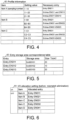
- FIG. 3 is a diagram showing the unit operation setting 61 stored in the storage part Una of the I/O unit Un.
- the unit operation setting 61 is data describing operations of the I/O unit Un.
- the unit operation setting 61 indicates a relation between items (parameters) of the input data acquired and transferred from the input devices such as the sensors 5 or the like by the I/O unit Un and setting values related to the items of the input data.
- the unit operation setting 61 is illustrated as a table in which the setting value is associated with each item of the input data, but the form of the unit operation setting 61 is not limited to the table.
- the item of the input data can include, for example, sampling times (acquisition times of data) of the analog data acquired by the sensors 5 and the like, a sampling interval, and a size of the data acquired from the input devices such as the sensors 5 and the like.
- the unit operation setting 61 is created by the user based on the profile information 62 ( FIG. 4 ) stored in the I/O management information storing part 60 of the I/O allocation management apparatus 10.
- the unit operation setting 61 created in the I/O allocation management apparatus 10 is stored in the I/O management information storing part 60 and is transferred from the I/O allocation management apparatus 10 to each I/O unit Un. Then, the unit operation setting 61 transferred to the I/O unit Un is stored in the storage part Una of each I/O unit Un.
- the I/O unit Un acquires the input data from the sensors 5 and transfers the acquired input data to the controller 20 based on the setting value set for each of the items set in the unit operation setting 61.
- FIG. 4 is a diagram showing the profile information 62 stored in the storage part of the I/O allocation management apparatus 10.
- the profile information 62 indicates, when the setting value of the unit operation setting 61 ( FIG. 3 ) is changed, an allocation relation between the changed setting value and a storage area (a storage area in the I/O memory 24a) required for the storage of the input data of the I/O unit Un based on the changed setting value.
- the profile information 62 is a static file which describes identification information or characteristics and the like of the I/O unit Un (a type and a size of I/O). Items and values (type and range) which can be set for the I/O unit Un may be included.
- a range of the setting value of each item is associated with an entry required for allocation in each range of the setting value.
- FIG. 5 is a diagram showing the entry storage area correspondence table 63 stored in the storage part of the I/O allocation management apparatus 10.
- the entry In the entry storage area correspondence table 63, the entry, the position of the storage area in the I/O memory 24a and the storage capacity (size) which can be stored in the storage area are associated.
- the entry storage area correspondence table 63 may be a table or other data forms.
- FIG. 6 is a diagram showing the I/O allocation setting 64 before mismatch elimination and stored in the communication module 24 of the controller 20.
- the I/O allocation setting 64 is data indicating a relation between the input data transferred from the sensors 5 to the I/O unit Un and the entry which is a variable number that specifies the storage area, wherein the storage area is within a plurality of storage areas included in the I/O memory 24a of the transfer destination to which the input data is transferred by the I/O unit Un and is allocated as the transfer destination of the input data.
- the I/O allocation setting 64 is created by the user using the I/O allocation management apparatus 10.
- the I/O allocation setting 64 created by the I/O allocation management apparatus 10 is stored in the I/O management information storing part 60, and is transferred from the I/O allocation management apparatus 10 to the communication module 24 of the controller 20.
- FIG. 6 a state is shown that the mismatch occurs in the allocation state between the input data and the storage area.
- FIG. 7 is a diagram showing the I/O allocation setting 64 after mismatch elimination and stored in the communication module 24 of the controller 20.
- an I/O allocation setting 64b is shown which shows a state that the mismatch occurring in the allocation state between the input data and the storage area is eliminated.
- FIG. 8 is a diagram showing the I/O map 65 stored in the storage part 22 of the controller 20.
- the I/O map 65 is data which describes a position of the storage area of the I/O memory 24a of the communication module 24 allocated to the storage part 22 (a CPU memory and the like) of the controller 20 and so on.
- the I/O map 65 is data which is created from the I/O allocation setting 64 and in which the I/O allocation setting 64 ( FIG. 6 and FIG. 7 ) created for each port is described.
- the I/O map 65 created by the I/O allocation management apparatus 10 is stored in the I/O management information storing part 60, and is also transferred to and stored in the storage part 22 of the controller 20.
- FIG. 9 is a diagram showing the setting screen 12A displayed on the display part 11 of the I/O allocation management apparatus 10.
- FIG. 10 is a diagram showing the warning screen 12B displayed on the display part 11 of the I/O allocation management apparatus 10.
- FIG. 11 is a diagram showing the specific warning screen 12Ba displayed on the display part 11 of the I/O allocation management apparatus 10.
- FIG. 12 is a diagram showing the I/O allocation situation screen 12C before the elimination of problems and displayed on the display part 11 of the I/O allocation management apparatus 10.
- FIG. 13 is a diagram showing the I/O allocation situation screen 12C after the elimination of problems and displayed on the display part 11 of the I/O allocation management apparatus 10.
- FIG. 14 is a flow chart showing a processing flow of the I/O allocation management apparatus 10 of embodiment 1.
- FIG. 9-FIG. 13 An example of the input screens displayed by the display part 11 is shown in FIG. 9-FIG. 13 .
- the input screens displayed by the display part 11 are not limited to the configurations shown in FIG. 9-FIG. 13 .
- the setting screen 12A shown in FIG. 9 is an input screen which receives an input operation of the user for changing the operation setting of the I/O unit Un.
- the setting screen 12 mainly displays content set by the unit operation setting 61.
- the allocation management part 41 displays the setting screen 12A in the display part 11 with reference to the unit operation setting 61 stored in the I/O management information storing part 60. For example, in the example shown in FIG. 9 , a port selecting button 12a, an editing start button 12b, and a unit operation setting table 12c are displayed on the setting screen 12A.
- a table 12c is displayed in which a corresponding relation between the present items and the setting values is described for each channel.
- a setting situation of the port selected by the user in the port selection button 12a is displayed in the table 12c.
- the allocation management part 41 displays the setting screen 12A on the display part 11 with reference to the unit operation setting 61 stored in the I/O management information storing part 60.
- the allocation management part 41 changes the setting value of the unit operation setting 61 corresponding to the change (step S11). For example, by the user, the setting value of item A (sampling number) in the port P1 and the channel ch1 is changed from a value A1 (10 times) to a value A2 (20 times) and the setting value of item C is changed from a value C2 to a value C1.
- the allocation management part 41 specifies an entry (a variable number) required for the storage of the input data based on the changed setting value with reference to the profile information 62 ( FIG. 4 ) stored in the I/O management information storing part 60 (step S12).
- the allocation management part 41 specifies that an entry required for the storage of the input data based on a value 20 which is the setting value after being change of the item A (sampling number) in the channel ch1 is entries EN011 and EN012, and specifies that an entry required for the storage of the input data based on the value C1 which is the setting value after being changed of the item C in the channel ch1 is an entry EN031.
- the entry storage area correspondence table 63 ( FIG. 5 )
- the position of the storage area within a plurality of storage areas in the I/O memory 24a and corresponding to the entry and the storage capacity (size) of the storage area are specified.
- the allocation management part 41 compares input data and the entry allocated to the input data specified in the I/O allocation setting 64a with an entry required for the storage of the input data based on the changed setting value and specified in step S12, and judges whether the presently allocated entry is excessive or insufficient (step S13).
- the allocation management part 41 judges whether the mismatch occurs in the allocation state between the input data and the storage area. Furthermore, the occurrence of mismatch refers to a state that the storage capacity of the storage area specified in the I/O allocation setting 64 (in other words, the number of the allocated entry) is insufficient or excessive with respect to the storage capacity required for the storage of the input data based on the changed setting value.
- the allocation management part 41 judges whether the mismatch occurs in the allocation state between the input data allocated before the change of the setting value and the storage area in the I/O memory 24a. Accordingly, when the mismatch of the allocation state occurs, by informing the user of the judgment result, the user can easily recognize an occurrence of the mismatch of the allocation state. Therefore, an occurrence of the mismatch between the storage capacity of the input data generated along with the change of the setting value and the storage capacity of the presently allocated storage area can be prevented from being overlooked. As a result, the problems can be prevented that the controller 20 cannot acquire a correct value and operates incorrectly or a robot operates incorrectly or the like due to leaving out a mismatch that requires a change.
- the allocation management part 41 can specify the storage capacity required for the storage of the input data based on the changed setting value.
- step S13 with reference to the I/O allocation setting 64a ( FIG. 6 ), the allocation management part 41 judges that because only the entry EN011 is presently allocated to the item A in the channel ch1, the necessary entry is insufficient (the mismatch occurs) with respect to the entries EN011 and EN012 required for the storage of the input data based on the changed setting value of the item A specified in step S12 ("YES" in step S13).
- step S13 with reference to the I/O allocation setting 64a ( FIG. 6 ), the allocation management part 41 judges that because the entries EN031 and EN032 are presently allocated to the item C in the channel ch1, the necessary entry is excessive (the mismatch occurs) with respect to the entry EN031 required for the storage of the input data based on the changed setting value of the item C in step S12 ("YES" in step S13).
- step S13 if the allocation management part 41 judges that the present allocated entry is not excessive or insufficient (that is, the mismatch does not occur) ("NO" in step S13), the flow is completed.
- step S13 When the allocation management part 41 judges that the present allocated entry is excessive or insufficient (that is, the mismatch occurs) in step S13 ("YES" in step S13), the warning screen 12B including warning information 12g which is notification information notified by the notification part 42 is displayed on the display part 11 (step S14).
- warning screen 12B As shown in FIG. 10 , on the warning screen 12B, for example, channel information 12d of each port indicating the channel arranged in each port, selection buttons 12f arranged in each port, and warning information 12g associated with the port within the plurality of ports and in which the mismatch occurs are displayed.
- the channel information 12d of each port the information is displayed that the channels ch1-ch4 which receive input of signals are respectively arranged on the ports P1-P4.
- the warning information 12g is displayed associated with channel information 12da of the port P1 in the channel information 12d of each port. Accordingly, the user can easily specify which is the I/O unit Un within a plurality of I/O units Un connected to the controller 20 to which the mismatch occurs in the allocation state.
- the allocation management part 41 displays the specific warning screen 12Ba related to the port P1 on the display part 11.
- the specific information of port P1 and the warning information 12g associated with the item in which the mismatch occurs are displayed on the specific warning screen 12Ba.
- the item and setting value (the changed setting value when the setting value is changed in step S11) of each channel in the port P1 and the warning information 12g respectively corresponding to the items A and C of the channel chl in which the mismatch occurs are displayed.
- the user pushes (selects) the editing start button 12b that changes the I/O allocation setting in order to eliminate the mismatch (step S15).
- the allocation management part 41 displays the item in which the mismatch occurs is displayed as a list on the display part 11 (step S16).
- the items A and C in which the mismatch occurs are displayed as a list in a table 12k.
- the items A and C in which the mismatch occurs and information of each item such as the setting value (the changed setting value), the allocated entry, and the storage capacity (size) of the storage area specified according to the entry are displayed.
- the allocation management part 41 judges whether to change all items having the mismatch on the I/O allocation situation screen 12C together (to eliminate the mismatch) (step S17).
- a checkbox 12m1 for selecting the item A is displayed corresponding to the item A; a checkbox 12m2 for selecting the item C is displayed corresponding to the item C; and a checkbox 12m0 for switching a selected state and a -non-selected state of the checkboxes 12m1 and 12m2 together is displayed outside the table 12k.
- the allocation management part 41 judges that all items having the mismatch on the I/O allocation situation screen 12C are to be changed (to eliminate the mismatch) together ("YES" in step S17).
- step S17 if the allocation management part 41 judges that all items having the mismatch on the I/O allocation situation screen 12C are to be changed (to eliminate the mismatch) together ("YES" in step S17), the mismatch of the item in which the mismatch occurs is eliminated (step S18), and an I/O allocation situation screen 12Cb on which the mismatch is eliminated is displayed on the display part 11.
- the allocation management part 41 adds the entry allocated to the item A by allocating the entry EN011 and the entry EN012 to the item A in which the value A2 is set as the setting value, and reduces the number of the entry allocated to the item C by only allocating the entry EN031 to the item C in which the value C1 is set as the setting value.
- the allocation management part 41 judges whether to confirm the changed allocation state based on the input from the user (step S19).
- the allocation management part 41 judges that the changed allocation state is to be confirmed ("YES" in step S19).
- the allocation management part 41 reflects the changed allocation state (the correspondence relation between the item and the allocated entry) on the I/O allocation setting 64 stored in the I/O management information storing part 60, creates and saves the I/O allocation setting 64 after the mismatch is eliminated.
- the entry EN011 is allocated to the item A and the entries EN031 and EN032 are allocated to the item C.
- the number of the entry allocated to the item A increases and the entries EN011 and EN012 are allocated, and the number of the entry allocated to the item C decreases and the entry EN031 is allocated.
- the allocation management part 41 confirms the changed allocation state (step S20), and transmits the I/O allocation setting 64 after mismatch elimination to the communication module 24. Furthermore, the allocation management part 41 updates the I/O map 65 based on the I/O allocation setting 64 after mismatch elimination, stores the updated I/O map 65 in the I/O management information storing part 60 and transmits the updated I/O map 65 to the storage part 22 of the controller 20.
- the flow is finished in this way.
- step S19 When the allocation management part 41 judges that the change of the changed allocation state is to be cancelled ("NO" in step S19) because a cancel button 12p in FIG. 13 is selected by the user and so on in step S19, the allocation management part 41 cancels the change of the allocation state (step S23) and finishes the flow. That is, instead of reflecting the allocation state between the items and entries displayed in the I/O allocation situation screen 12C of FIG. 13 on the I/O allocation setting 64, the allocation management part 41 maintains the state of the I/O allocation setting 64 shown in FIG. 6 and finishes the flow.
- step S17 if any one of the checkboxes 12m1 and 12m2 shown in FIG. 12 is selected and the mismatch eliminating button 12j is selected, the allocation management part 41 judges that not all the items having the mismatch on the I/O allocation situation screen 12C are to be changed together (not to eliminate the mismatches together) ("NO" in step S17). Then, the allocation management part 41 only changes the allocation state of the item selected in step S17 (step S22), and the I/O allocation situation screen 12C shown in FIG. 13 is displayed on the display part 11.
- step S19 the flow proceeds to "YES” in step S19 and the processing of step S20, or "NO” in step S19 and the processing of step S23.
- step S19 the allocation management part 41 informs the user of the changed allocation state between the input data and the storage area before confirming the change of the allocation state between the input data and the storage area specified in the I/O allocation setting 64 ( FIG. 6 ), and facilitates the user to determine whether the allocation state is to be changed in the input. In this way, the allocation state unintended by the user can be prevented.
- step S13 if the allocation management part 41 judges that the mismatch of the allocation state occurs, the allocation state between the input data and the storage area specified in the I/O allocation setting 64 is changed and the change is confirmed in step S20 so that the storage capacity required for the storage of the input data based on the changed setting value is ensured.
- the allocation management part 41 instead of the user, the allocation state between the input data and the storage area specified in the I/O allocation setting 64 is changed so that the storage capacity required for the storage of the input data based on the changed setting value is ensured. Accordingly, the trouble of the user changing the allocation state between the input data and the storage area is avoided; furthermore, a change miss of the allocation state caused by the user can be prevented. Accordingly, unintentional stop of the operation of the I/O unit can be more reliably prevented.
- the storage capacity (that is, the number of entry) specified in the I/O allocation setting 64 is insufficient with respect to the storage capacity required for the storage of the input data based on the changed setting value, such as the case in FIG. 12 that only the entry EN011 is allocated to the item A in which the value A2 is set as the setting value, the input data cannot be transferred from the I/O unit Un to the controller 20, and thus the elimination of mismatch of the allocation state is required.
- the input data can be transferred from the I/O unit Un to the controller 20, and thus whether to eliminate the mismatch of the allocation state is optionally set by the user.
- the allocation management part 41 judges that the mismatch occurs in the allocation state, the information indicating whether the elimination of mismatch of the allocation state is required or optional may be displayed in the display part 11.
- the checkbox 12m1 corresponding to the item A may be displayed forcibly as the selected state so as not to be released of selection by the user; on the other hand, the checkbox 12m2 corresponding to the item C may be displayed so as to be optionally selected by the user whether to become the selected state or the non-selected state.
- the user when viewing the I/O allocation situation screen 12C shown in FIG. 12 , the user can determine whether the elimination of mismatch of the allocation state is required or optional. In this way, only the minimum necessary elimination of mismatch is performed and thus the trouble of the user can be reduced.
- the controller 20 may also be connected to the I/O unit Un via a communication coupler.
- the communication coupler is connected to the controller 20 via a network
- the I/O unit Un is connected to the communication coupler.
- the input data to the I/O unit Un is transmitted to the communication coupler and is transmitted from the communication coupler to the controller 20.
- the I/O memory 24a may be arranged not on the controller 20 but on the communication coupler.
- the I/O allocation setting is stored in the communication coupler.
- a control block (especially the allocation management part 41 and the notification part 42) of the I/O allocation management apparatus 10 may be implemented by a logic circuit (hardware) formed in an integrated circuit (IC chip) and the like, or may be implemented by software.
- the I/O allocation management apparatus 10 is provided with a computer that executes commands of a program which is software for realizing each function.
- the computer includes, for example, one or more processors and a computer readable recording medium in which the above program is stored. Then, the processor reads the program from the recording medium and executing the program in the computer, thereby achieving the purpose of the invention.
- a processor for example, a CPU (Central Processing Unit) can be used.
- a "non-transitory tangible media" for example, besides a ROM (Read Only Storage) and the like, a tape, a disk, a card, a semiconductor memory, a programmable logic circuit and the like can be used.
- a RAM Random Access Storage
- the program may be supplied to the computer via an optional transmission medium (a communication network or a broadcast wave or the like) capable of transmitting the program.
- an optional transmission medium a communication network or a broadcast wave or the like
- one aspect of the disclosure can also be implemented in a form of a data signal which is embedded in a carrier wave and in which the program is embodied by an electronic transmission.
Landscapes
- Engineering & Computer Science (AREA)
- Theoretical Computer Science (AREA)
- Physics & Mathematics (AREA)
- General Engineering & Computer Science (AREA)
- General Physics & Mathematics (AREA)
- Human Computer Interaction (AREA)
- Automation & Control Theory (AREA)
- Computing Systems (AREA)
- Quality & Reliability (AREA)
- Mathematical Physics (AREA)
- Programmable Controllers (AREA)
Claims (8)
- E/A-Moduleinheit (1), die umfasst:eine E/A-Einheit (Un), die konfiguriert ist, um mit Eingabevorrichtungen (5) verbunden zu werden und Eingabedaten von den Eingabevorrichtungen (5) zu erfassen, die als Sensoren verwendet werden, die an einer in einer Fabrik verwendeten Steuerobjektvorrichtung angeordnet sind;eine Steuerung (20), die konfiguriert ist, um die E/A-Einheit zu steuern; undeine E/A-Zuweisungsverwaltungsvorrichtung (10), die konfiguriert ist, um mit der E/A-Einheit (Un) und der Steuerung (20) verbunden zu sein und die E/A-Einheit (Un) zu verwalten, wobei die E/A-Zuweisungsverwaltungsvorrichtung (10) umfasst:ein E/A-Verwaltungsinformationsspeicherteil (60), das speichert:eine Einheitsbetriebseinstellung (61), die eine Beziehung zwischen Eingangsdaten, die von den Eingabevorrichtungen (5) durch die E/A-Einheit (Un) erfasst und übertragen werden, und einen auf die Eingangsdaten bezogenen Einstellwert anzeigt, undeine E/A-Zuordnungseinstellung (64), die eine Beziehung zwischen den Eingabedaten und Spezifikationsinformationen anzeigt, die einen Speicherbereich spezifizieren, wobei der Speicherbereich innerhalb einer Vielzahl von Speicherbereichen liegt, die in einem Speicherteil eines Übertragungsziels enthalten sind, an das die Eingabedaten durch die E/A-Einheit (Un) übertragen werden und als das Übertragungsziel der Eingabedaten zugewiesen werden; undein Zuweisungsverwaltungsteil (41), das, angepasst wird, wenn der Einstellwert in der Einheitsbetriebseinstellung (61) geändert wird, um zu spezifizieren, ob basierend auf einem geänderten Einstellwert, eine Speicherkapazität, erforderlich für eine Speicherung der Eingabedaten, erzeugt entlang der Änderung des Einstellwerts, und um festzustellen, obin einem Zuweisungszustand eine Nichtübereinstimmung zwischen der erforderlichen Speicherkapazität der Eingabedaten und dem Speicherbereich, spezifiziert in der E/A-Zuordnungseinstellung (64), auftritt und zugewiesen vor der Änderung des Einstellwerts; wobei die E/A Moduleinheit (1) angepasst ist, um einen Benutzer über das Bewertungsergebnis zu informieren.
- E/A-Moduleinheit (1) gemäß Anspruch 1, wobei, wenn der Einstellwert in der Einheitsbetriebseinstellung (61) geändert wird,
das Zuweisungsverwaltungsteil (41) die Speicherkapazität spezifiziert, die für die Speicherung der Eingabedaten basierend auf dem geänderten Einstellwert erforderlich ist, indem er sich auf Profilinformationen (62) bezieht, die eine Zuweisungsbeziehung zwischen dem geänderten Einstellwert und dem Speicherbereich anzeigen, der für die Speicherung der Eingabedaten basierend auf dem geänderten Einstellwert erforderlich ist. - E/A-Moduleinheit (1) gemäß Anspruch 1 oder 2, wobei, wenn das Zuweisungsverwaltungsteil (41) feststellt, dass die Nichtübereinstimmung des Zuweisungszustands auftritt, der Zuweisungszustand zwischen den Eingabedaten und dem in der E/A-Zuweisungseinstellung (64) spezifizierten Speicherbereich geändert wird und eine Tatsache der Änderung bestätigt wird, so dass die Speicherkapazität, erforderlich für die Speicherung der Eingabedaten basierend auf dem geänderten Einstellungswert, gewährleistet ist.
- E/A-Moduleinheit (1) gemäß Anspruch 3, wobei das Zuweisungsverwaltungsteil (41) einen Benutzer über den geänderten Zuweisungszustand zwischen den Eingabedaten und dem Speicherbereich informiert, bevor der geänderte Zuweisungszustand zwischen den Eingabedaten und dem gespeicherten Bereich, spezifiziert in der E/A-Zuweisungseinstellung (64) bestätigt wird, und dem Benutzer eine Eingabe erleichtert, um zu bestimmen, ob der Zuweisungszustand zu ändern ist.
- E/A-Moduleinheit (1) gemäß einem der Ansprüche 1 bis 4, wobei die E/A-Zuordnungsverwaltungsvorrichtung (10) ferner ein Anzeigeteil (11) umfasst, das einen Eingabebildschirm anzeigt, der die Eingabe des Benutzers erleichtert, und
Verwalten einer Vielzahl von E/A-Einheiten (Un1~Unn), die mit der Steuerung (20) verbunden sind. - E/A-Moduleinheit (1) gemäß Anspruch 5, wobei die E/A-Zuweisungsverwaltungsvorrichtung (10) ferner ein Benachrichtigungsteil (42) umfasst, das den Benutzer über die in dem Zuweisungszustand auftretende Nichtübereinstimmung benachrichtigt, wenn das Zuweisungsverwaltungsteil (41) feststellt, dass die Nichtübereinstimmung in dem Zuweisungszustand auftritt.
- E/A-Moduleinheit (1) gemäß Anspruch 6, wobei, wenn das Zuweisungsverwaltungsteil (41) feststellt, dass die Nichtübereinstimmung in dem Zuweisungszustand auftritt, das Benachrichtigungsteil (42) eine Benachrichtigung ausgibt, durch Anzeigen auf dem Eingabebildschirm eine Warninformation, die der E/A-Einheit (Un) entspricht, die sich innerhalb einer Vielzahl von E/A-Einheiten (Un1~Unn) befindet und bei der die Nichtübereinstimmung in dem Zuweisungszustand auftritt.
- E/A-Moduleinheit (1) gemäß einem der Ansprüche 5 bis 7, wobei, wenn das Zuordnungsverwaltungsteil (41) feststellt, dass die Nichtübereinstimmung in dem Zuordnungszustand auftritt, auf dem Eingabebildschirm Informationen angezeigt werden, die angeben, ob die Beseitigung der Nichtübereinstimmung des Zuordnungszustands erforderlich oder optional ist.
Applications Claiming Priority (1)
| Application Number | Priority Date | Filing Date | Title |
|---|---|---|---|
| JP2018030046A JP7027947B2 (ja) | 2018-02-22 | 2018-02-22 | I/o管理装置 |
Publications (2)
| Publication Number | Publication Date |
|---|---|
| EP3531218A1 EP3531218A1 (de) | 2019-08-28 |
| EP3531218B1 true EP3531218B1 (de) | 2024-04-03 |
Family
ID=64316319
Family Applications (1)
| Application Number | Title | Priority Date | Filing Date |
|---|---|---|---|
| EP18206161.4A Active EP3531218B1 (de) | 2018-02-22 | 2018-11-14 | E/a-modul |
Country Status (4)
| Country | Link |
|---|---|
| US (1) | US10789187B2 (de) |
| EP (1) | EP3531218B1 (de) |
| JP (1) | JP7027947B2 (de) |
| CN (1) | CN110188020B (de) |
Families Citing this family (4)
| Publication number | Priority date | Publication date | Assignee | Title |
|---|---|---|---|---|
| JP7044383B2 (ja) * | 2019-08-06 | 2022-03-30 | 株式会社ニューギン | 遊技機 |
| US12273141B2 (en) * | 2023-03-22 | 2025-04-08 | International Business Machines Corporation | Optical cable mismatch error detection/remediation |
| JP2025152700A (ja) * | 2024-03-28 | 2025-10-10 | 横河電機株式会社 | コントローラ |
| JP2025152699A (ja) * | 2024-03-28 | 2025-10-10 | 横河電機株式会社 | 制御プログラム及びコントローラ |
Citations (2)
| Publication number | Priority date | Publication date | Assignee | Title |
|---|---|---|---|---|
| JP2008059532A (ja) * | 2006-09-04 | 2008-03-13 | Omron Corp | 制御システム設定管理システム |
| JP2013225251A (ja) * | 2012-04-23 | 2013-10-31 | Mitsubishi Electric Corp | 情報処理装置及び情報処理方法及びプログラム |
Family Cites Families (11)
| Publication number | Priority date | Publication date | Assignee | Title |
|---|---|---|---|---|
| JPS6219950A (ja) * | 1985-07-18 | 1987-01-28 | Fujitsu Ltd | 記憶装置のアドレスエラ−検出方式 |
| US5951658A (en) * | 1997-09-25 | 1999-09-14 | International Business Machines Corporation | System for dynamic allocation of I/O buffers for VSAM access method based upon intended record access where performance information regarding access is stored in memory |
| JPH11338512A (ja) * | 1998-05-26 | 1999-12-10 | Matsushita Electric Works Ltd | 表示器 |
| JP2005327263A (ja) * | 2004-04-13 | 2005-11-24 | Omron Corp | 制御システム設定装置 |
| US7890669B2 (en) * | 2005-11-25 | 2011-02-15 | Hitachi, Ltd. | Computer system for sharing I/O device |
| JP4905810B2 (ja) * | 2008-10-01 | 2012-03-28 | 日本電気株式会社 | ストレージ装置、領域割り当て方法、及びプログラム |
| JP2013167798A (ja) * | 2012-02-16 | 2013-08-29 | Canon Inc | 画像生成装置及びその制御方法 |
| DE112013004360B4 (de) * | 2012-09-05 | 2021-12-30 | Mitsubishi Electric Corporation | Eingabe/Ausgabe-Ansprechsteuerungseinstellungseinrichtung |
| JP6052265B2 (ja) | 2014-10-21 | 2016-12-27 | 横河電機株式会社 | I/oモジュール、設定装置、及びプロセス制御システムの構築方法 |
| WO2016088229A1 (ja) | 2014-12-03 | 2016-06-09 | 三菱電機株式会社 | 入出力機器 |
| JP2017162108A (ja) | 2016-03-08 | 2017-09-14 | 株式会社東芝 | I/oモジュール管理装置、i/oモジュール管理方法 |
-
2018
- 2018-02-22 JP JP2018030046A patent/JP7027947B2/ja active Active
- 2018-11-13 US US16/188,292 patent/US10789187B2/en active Active
- 2018-11-14 CN CN201811352298.7A patent/CN110188020B/zh active Active
- 2018-11-14 EP EP18206161.4A patent/EP3531218B1/de active Active
Patent Citations (2)
| Publication number | Priority date | Publication date | Assignee | Title |
|---|---|---|---|---|
| JP2008059532A (ja) * | 2006-09-04 | 2008-03-13 | Omron Corp | 制御システム設定管理システム |
| JP2013225251A (ja) * | 2012-04-23 | 2013-10-31 | Mitsubishi Electric Corp | 情報処理装置及び情報処理方法及びプログラム |
Also Published As
| Publication number | Publication date |
|---|---|
| JP7027947B2 (ja) | 2022-03-02 |
| CN110188020A (zh) | 2019-08-30 |
| US20190258595A1 (en) | 2019-08-22 |
| US10789187B2 (en) | 2020-09-29 |
| EP3531218A1 (de) | 2019-08-28 |
| CN110188020B (zh) | 2023-06-16 |
| JP2019144956A (ja) | 2019-08-29 |
Similar Documents
| Publication | Publication Date | Title |
|---|---|---|
| EP3531218A1 (de) | E/a-verwaltungsvorrichtung | |
| EP2966617B1 (de) | System umfassend vorrichtung zur bilddatenerzeugung und tragbare endgerätevorrichtung | |
| CN114114976A (zh) | 半导体制造系统、控制装置、控制方法和存储介质 | |
| US10261716B2 (en) | Programmable display, update processing apparatus, updating method, information processing method, and program stored on computer-readable recording medium | |
| CN102087593A (zh) | 远程设备管理界面 | |
| US10499051B2 (en) | Display device provided with video display unit, and method for measuring display of video display unit | |
| CN107407922B (zh) | 可编程逻辑控制器及其控制方法以及记录介质 | |
| EP3026556A1 (de) | Ereigniserzeugungsmanagement für einen industrieregler | |
| US20170346982A1 (en) | Function execution method, information processing apparatus, and non-transitory recording medium storing instructions for information processing apparatus | |
| US9342219B2 (en) | Method for adapting the graphic representation on the user interface of a computer user station | |
| KR20170129229A (ko) | 정보 처리 장치, 정보 처리 시스템 및 기록 매체 | |
| EP2960898A1 (de) | Bilddatenerzeugungsvorrichtung und programmierbare Anzeigevorrichtung | |
| US7825916B2 (en) | Controller, mobile terminal apparatus, and program | |
| CN107132809A (zh) | 可编程控制器及可编程控制器的控制程序 | |
| US10740092B2 (en) | Protection and control system | |
| CN113424116B (zh) | 设定信息生成装置、设定信息生成方法及记录介质 | |
| JP2007249748A (ja) | バージョン管理機能を有するネットワーク機器 | |
| JP5295079B2 (ja) | プログラムダウンロード装置及びプログラムダウンロード方法 | |
| US20070282469A1 (en) | Data processing unit and data processing method | |
| US8175569B2 (en) | Device control | |
| US20260036978A1 (en) | Information processing method, substrate processing system, and computer-readable recording medium | |
| US11860600B2 (en) | Programmable display device with user input configuration adjustment | |
| EP3731045B1 (de) | Steuersystem, steuerverfahren und nichtflüchtiges speichermedium | |
| CN115840549B (zh) | 多个显控终端之间突发信息同步方法、系统、设备和介质 | |
| CA3043701A1 (en) | Connection device restriction system |
Legal Events
| Date | Code | Title | Description |
|---|---|---|---|
| PUAI | Public reference made under article 153(3) epc to a published international application that has entered the european phase |
Free format text: ORIGINAL CODE: 0009012 |
|
| STAA | Information on the status of an ep patent application or granted ep patent |
Free format text: STATUS: REQUEST FOR EXAMINATION WAS MADE |
|
| 17P | Request for examination filed |
Effective date: 20181114 |
|
| AK | Designated contracting states |
Kind code of ref document: A1 Designated state(s): AL AT BE BG CH CY CZ DE DK EE ES FI FR GB GR HR HU IE IS IT LI LT LU LV MC MK MT NL NO PL PT RO RS SE SI SK SM TR |
|
| AX | Request for extension of the european patent |
Extension state: BA ME |
|
| RBV | Designated contracting states (corrected) |
Designated state(s): AL AT BE BG CH CY CZ DE DK EE ES FI FR GB GR HR HU IE IS IT LI LT LU LV MC MK MT NL NO PL PT RO RS SE SI SK SM TR |
|
| STAA | Information on the status of an ep patent application or granted ep patent |
Free format text: STATUS: EXAMINATION IS IN PROGRESS |
|
| 17Q | First examination report despatched |
Effective date: 20210706 |
|
| GRAP | Despatch of communication of intention to grant a patent |
Free format text: ORIGINAL CODE: EPIDOSNIGR1 |
|
| STAA | Information on the status of an ep patent application or granted ep patent |
Free format text: STATUS: GRANT OF PATENT IS INTENDED |
|
| INTG | Intention to grant announced |
Effective date: 20231215 |
|
| GRAS | Grant fee paid |
Free format text: ORIGINAL CODE: EPIDOSNIGR3 |
|
| GRAA | (expected) grant |
Free format text: ORIGINAL CODE: 0009210 |
|
| STAA | Information on the status of an ep patent application or granted ep patent |
Free format text: STATUS: THE PATENT HAS BEEN GRANTED |
|
| AK | Designated contracting states |
Kind code of ref document: B1 Designated state(s): AL AT BE BG CH CY CZ DE DK EE ES FI FR GB GR HR HU IE IS IT LI LT LU LV MC MK MT NL NO PL PT RO RS SE SI SK SM TR |
|
| REG | Reference to a national code |
Ref country code: GB Ref legal event code: FG4D |
|
| REG | Reference to a national code |
Ref country code: CH Ref legal event code: EP |
|
| REG | Reference to a national code |
Ref country code: IE Ref legal event code: FG4D |
|
| REG | Reference to a national code |
Ref country code: DE Ref legal event code: R096 Ref document number: 602018067427 Country of ref document: DE |
|
| REG | Reference to a national code |
Ref country code: LT Ref legal event code: MG9D |
|
| REG | Reference to a national code |
Ref country code: NL Ref legal event code: MP Effective date: 20240403 |
|
| REG | Reference to a national code |
Ref country code: AT Ref legal event code: MK05 Ref document number: 1673033 Country of ref document: AT Kind code of ref document: T Effective date: 20240403 |
|
| PG25 | Lapsed in a contracting state [announced via postgrant information from national office to epo] |
Ref country code: NL Free format text: LAPSE BECAUSE OF FAILURE TO SUBMIT A TRANSLATION OF THE DESCRIPTION OR TO PAY THE FEE WITHIN THE PRESCRIBED TIME-LIMIT Effective date: 20240403 |
|
| PG25 | Lapsed in a contracting state [announced via postgrant information from national office to epo] |
Ref country code: NL Free format text: LAPSE BECAUSE OF FAILURE TO SUBMIT A TRANSLATION OF THE DESCRIPTION OR TO PAY THE FEE WITHIN THE PRESCRIBED TIME-LIMIT Effective date: 20240403 |
|
| PG25 | Lapsed in a contracting state [announced via postgrant information from national office to epo] |
Ref country code: IS Free format text: LAPSE BECAUSE OF FAILURE TO SUBMIT A TRANSLATION OF THE DESCRIPTION OR TO PAY THE FEE WITHIN THE PRESCRIBED TIME-LIMIT Effective date: 20240803 |
|
| PG25 | Lapsed in a contracting state [announced via postgrant information from national office to epo] |
Ref country code: BG Free format text: LAPSE BECAUSE OF FAILURE TO SUBMIT A TRANSLATION OF THE DESCRIPTION OR TO PAY THE FEE WITHIN THE PRESCRIBED TIME-LIMIT Effective date: 20240403 |
|
| PG25 | Lapsed in a contracting state [announced via postgrant information from national office to epo] |
Ref country code: HR Free format text: LAPSE BECAUSE OF FAILURE TO SUBMIT A TRANSLATION OF THE DESCRIPTION OR TO PAY THE FEE WITHIN THE PRESCRIBED TIME-LIMIT Effective date: 20240403 Ref country code: FI Free format text: LAPSE BECAUSE OF FAILURE TO SUBMIT A TRANSLATION OF THE DESCRIPTION OR TO PAY THE FEE WITHIN THE PRESCRIBED TIME-LIMIT Effective date: 20240403 |
|
| PG25 | Lapsed in a contracting state [announced via postgrant information from national office to epo] |
Ref country code: GR Free format text: LAPSE BECAUSE OF FAILURE TO SUBMIT A TRANSLATION OF THE DESCRIPTION OR TO PAY THE FEE WITHIN THE PRESCRIBED TIME-LIMIT Effective date: 20240704 |
|
| PG25 | Lapsed in a contracting state [announced via postgrant information from national office to epo] |
Ref country code: PT Free format text: LAPSE BECAUSE OF FAILURE TO SUBMIT A TRANSLATION OF THE DESCRIPTION OR TO PAY THE FEE WITHIN THE PRESCRIBED TIME-LIMIT Effective date: 20240805 |
|
| PG25 | Lapsed in a contracting state [announced via postgrant information from national office to epo] |
Ref country code: ES Free format text: LAPSE BECAUSE OF FAILURE TO SUBMIT A TRANSLATION OF THE DESCRIPTION OR TO PAY THE FEE WITHIN THE PRESCRIBED TIME-LIMIT Effective date: 20240403 |
|
| PG25 | Lapsed in a contracting state [announced via postgrant information from national office to epo] |
Ref country code: CZ Free format text: LAPSE BECAUSE OF FAILURE TO SUBMIT A TRANSLATION OF THE DESCRIPTION OR TO PAY THE FEE WITHIN THE PRESCRIBED TIME-LIMIT Effective date: 20240403 |
|
| PG25 | Lapsed in a contracting state [announced via postgrant information from national office to epo] |
Ref country code: AT Free format text: LAPSE BECAUSE OF FAILURE TO SUBMIT A TRANSLATION OF THE DESCRIPTION OR TO PAY THE FEE WITHIN THE PRESCRIBED TIME-LIMIT Effective date: 20240403 |
|
| PG25 | Lapsed in a contracting state [announced via postgrant information from national office to epo] |
Ref country code: PL Free format text: LAPSE BECAUSE OF FAILURE TO SUBMIT A TRANSLATION OF THE DESCRIPTION OR TO PAY THE FEE WITHIN THE PRESCRIBED TIME-LIMIT Effective date: 20240403 |
|
| PG25 | Lapsed in a contracting state [announced via postgrant information from national office to epo] |
Ref country code: LV Free format text: LAPSE BECAUSE OF FAILURE TO SUBMIT A TRANSLATION OF THE DESCRIPTION OR TO PAY THE FEE WITHIN THE PRESCRIBED TIME-LIMIT Effective date: 20240403 |
|
| PG25 | Lapsed in a contracting state [announced via postgrant information from national office to epo] |
Ref country code: PT Free format text: LAPSE BECAUSE OF FAILURE TO SUBMIT A TRANSLATION OF THE DESCRIPTION OR TO PAY THE FEE WITHIN THE PRESCRIBED TIME-LIMIT Effective date: 20240805 Ref country code: PL Free format text: LAPSE BECAUSE OF FAILURE TO SUBMIT A TRANSLATION OF THE DESCRIPTION OR TO PAY THE FEE WITHIN THE PRESCRIBED TIME-LIMIT Effective date: 20240403 Ref country code: NO Free format text: LAPSE BECAUSE OF FAILURE TO SUBMIT A TRANSLATION OF THE DESCRIPTION OR TO PAY THE FEE WITHIN THE PRESCRIBED TIME-LIMIT Effective date: 20240703 Ref country code: LV Free format text: LAPSE BECAUSE OF FAILURE TO SUBMIT A TRANSLATION OF THE DESCRIPTION OR TO PAY THE FEE WITHIN THE PRESCRIBED TIME-LIMIT Effective date: 20240403 Ref country code: IS Free format text: LAPSE BECAUSE OF FAILURE TO SUBMIT A TRANSLATION OF THE DESCRIPTION OR TO PAY THE FEE WITHIN THE PRESCRIBED TIME-LIMIT Effective date: 20240803 Ref country code: HR Free format text: LAPSE BECAUSE OF FAILURE TO SUBMIT A TRANSLATION OF THE DESCRIPTION OR TO PAY THE FEE WITHIN THE PRESCRIBED TIME-LIMIT Effective date: 20240403 Ref country code: GR Free format text: LAPSE BECAUSE OF FAILURE TO SUBMIT A TRANSLATION OF THE DESCRIPTION OR TO PAY THE FEE WITHIN THE PRESCRIBED TIME-LIMIT Effective date: 20240704 Ref country code: FI Free format text: LAPSE BECAUSE OF FAILURE TO SUBMIT A TRANSLATION OF THE DESCRIPTION OR TO PAY THE FEE WITHIN THE PRESCRIBED TIME-LIMIT Effective date: 20240403 Ref country code: ES Free format text: LAPSE BECAUSE OF FAILURE TO SUBMIT A TRANSLATION OF THE DESCRIPTION OR TO PAY THE FEE WITHIN THE PRESCRIBED TIME-LIMIT Effective date: 20240403 Ref country code: CZ Free format text: LAPSE BECAUSE OF FAILURE TO SUBMIT A TRANSLATION OF THE DESCRIPTION OR TO PAY THE FEE WITHIN THE PRESCRIBED TIME-LIMIT Effective date: 20240403 Ref country code: BG Free format text: LAPSE BECAUSE OF FAILURE TO SUBMIT A TRANSLATION OF THE DESCRIPTION OR TO PAY THE FEE WITHIN THE PRESCRIBED TIME-LIMIT Effective date: 20240403 Ref country code: AT Free format text: LAPSE BECAUSE OF FAILURE TO SUBMIT A TRANSLATION OF THE DESCRIPTION OR TO PAY THE FEE WITHIN THE PRESCRIBED TIME-LIMIT Effective date: 20240403 Ref country code: RS Free format text: LAPSE BECAUSE OF FAILURE TO SUBMIT A TRANSLATION OF THE DESCRIPTION OR TO PAY THE FEE WITHIN THE PRESCRIBED TIME-LIMIT Effective date: 20240703 |
|
| REG | Reference to a national code |
Ref country code: DE Ref legal event code: R097 Ref document number: 602018067427 Country of ref document: DE |
|
| PGFP | Annual fee paid to national office [announced via postgrant information from national office to epo] |
Ref country code: DE Payment date: 20241126 Year of fee payment: 7 |
|
| PG25 | Lapsed in a contracting state [announced via postgrant information from national office to epo] |
Ref country code: DK Free format text: LAPSE BECAUSE OF FAILURE TO SUBMIT A TRANSLATION OF THE DESCRIPTION OR TO PAY THE FEE WITHIN THE PRESCRIBED TIME-LIMIT Effective date: 20240403 |
|
| PG25 | Lapsed in a contracting state [announced via postgrant information from national office to epo] |
Ref country code: EE Free format text: LAPSE BECAUSE OF FAILURE TO SUBMIT A TRANSLATION OF THE DESCRIPTION OR TO PAY THE FEE WITHIN THE PRESCRIBED TIME-LIMIT Effective date: 20240403 |
|
| PG25 | Lapsed in a contracting state [announced via postgrant information from national office to epo] |
Ref country code: RO Free format text: LAPSE BECAUSE OF FAILURE TO SUBMIT A TRANSLATION OF THE DESCRIPTION OR TO PAY THE FEE WITHIN THE PRESCRIBED TIME-LIMIT Effective date: 20240403 Ref country code: SK Free format text: LAPSE BECAUSE OF FAILURE TO SUBMIT A TRANSLATION OF THE DESCRIPTION OR TO PAY THE FEE WITHIN THE PRESCRIBED TIME-LIMIT Effective date: 20240403 |
|
| PG25 | Lapsed in a contracting state [announced via postgrant information from national office to epo] |
Ref country code: SM Free format text: LAPSE BECAUSE OF FAILURE TO SUBMIT A TRANSLATION OF THE DESCRIPTION OR TO PAY THE FEE WITHIN THE PRESCRIBED TIME-LIMIT Effective date: 20240403 |
|
| PG25 | Lapsed in a contracting state [announced via postgrant information from national office to epo] |
Ref country code: SM Free format text: LAPSE BECAUSE OF FAILURE TO SUBMIT A TRANSLATION OF THE DESCRIPTION OR TO PAY THE FEE WITHIN THE PRESCRIBED TIME-LIMIT Effective date: 20240403 Ref country code: SK Free format text: LAPSE BECAUSE OF FAILURE TO SUBMIT A TRANSLATION OF THE DESCRIPTION OR TO PAY THE FEE WITHIN THE PRESCRIBED TIME-LIMIT Effective date: 20240403 Ref country code: RO Free format text: LAPSE BECAUSE OF FAILURE TO SUBMIT A TRANSLATION OF THE DESCRIPTION OR TO PAY THE FEE WITHIN THE PRESCRIBED TIME-LIMIT Effective date: 20240403 Ref country code: EE Free format text: LAPSE BECAUSE OF FAILURE TO SUBMIT A TRANSLATION OF THE DESCRIPTION OR TO PAY THE FEE WITHIN THE PRESCRIBED TIME-LIMIT Effective date: 20240403 Ref country code: DK Free format text: LAPSE BECAUSE OF FAILURE TO SUBMIT A TRANSLATION OF THE DESCRIPTION OR TO PAY THE FEE WITHIN THE PRESCRIBED TIME-LIMIT Effective date: 20240403 |
|
| PLBE | No opposition filed within time limit |
Free format text: ORIGINAL CODE: 0009261 |
|
| STAA | Information on the status of an ep patent application or granted ep patent |
Free format text: STATUS: NO OPPOSITION FILED WITHIN TIME LIMIT |
|
| 26N | No opposition filed |
Effective date: 20250106 |
|
| PG25 | Lapsed in a contracting state [announced via postgrant information from national office to epo] |
Ref country code: SI Free format text: LAPSE BECAUSE OF FAILURE TO SUBMIT A TRANSLATION OF THE DESCRIPTION OR TO PAY THE FEE WITHIN THE PRESCRIBED TIME-LIMIT Effective date: 20240403 |
|
| REG | Reference to a national code |
Ref country code: CH Ref legal event code: PL |
|
| PG25 | Lapsed in a contracting state [announced via postgrant information from national office to epo] |
Ref country code: MC Free format text: LAPSE BECAUSE OF FAILURE TO SUBMIT A TRANSLATION OF THE DESCRIPTION OR TO PAY THE FEE WITHIN THE PRESCRIBED TIME-LIMIT Effective date: 20240403 |
|
| PG25 | Lapsed in a contracting state [announced via postgrant information from national office to epo] |
Ref country code: LU Free format text: LAPSE BECAUSE OF NON-PAYMENT OF DUE FEES Effective date: 20241114 |
|
| REG | Reference to a national code |
Ref country code: CH Ref legal event code: PL |
|
| GBPC | Gb: european patent ceased through non-payment of renewal fee |
Effective date: 20241114 |
|
| PG25 | Lapsed in a contracting state [announced via postgrant information from national office to epo] |
Ref country code: CH Free format text: LAPSE BECAUSE OF NON-PAYMENT OF DUE FEES Effective date: 20241130 |
|
| REG | Reference to a national code |
Ref country code: BE Ref legal event code: MM Effective date: 20241130 |
|
| PG25 | Lapsed in a contracting state [announced via postgrant information from national office to epo] |
Ref country code: SE Free format text: LAPSE BECAUSE OF FAILURE TO SUBMIT A TRANSLATION OF THE DESCRIPTION OR TO PAY THE FEE WITHIN THE PRESCRIBED TIME-LIMIT Effective date: 20240403 |
|
| PG25 | Lapsed in a contracting state [announced via postgrant information from national office to epo] |
Ref country code: GB Free format text: LAPSE BECAUSE OF NON-PAYMENT OF DUE FEES Effective date: 20241114 Ref country code: BE Free format text: LAPSE BECAUSE OF NON-PAYMENT OF DUE FEES Effective date: 20241130 |
|
| PG25 | Lapsed in a contracting state [announced via postgrant information from national office to epo] |
Ref country code: FR Free format text: LAPSE BECAUSE OF NON-PAYMENT OF DUE FEES Effective date: 20241130 |
|
| PG25 | Lapsed in a contracting state [announced via postgrant information from national office to epo] |
Ref country code: IE Free format text: LAPSE BECAUSE OF NON-PAYMENT OF DUE FEES Effective date: 20241114 |
|
| PG25 | Lapsed in a contracting state [announced via postgrant information from national office to epo] |
Ref country code: IT Free format text: LAPSE BECAUSE OF FAILURE TO SUBMIT A TRANSLATION OF THE DESCRIPTION OR TO PAY THE FEE WITHIN THE PRESCRIBED TIME-LIMIT Effective date: 20240403 |
|
| PG25 | Lapsed in a contracting state [announced via postgrant information from national office to epo] |
Ref country code: HU Free format text: LAPSE BECAUSE OF FAILURE TO SUBMIT A TRANSLATION OF THE DESCRIPTION OR TO PAY THE FEE WITHIN THE PRESCRIBED TIME-LIMIT; INVALID AB INITIO Effective date: 20181114 |
|
| PG25 | Lapsed in a contracting state [announced via postgrant information from national office to epo] |
Ref country code: CY Free format text: LAPSE BECAUSE OF FAILURE TO SUBMIT A TRANSLATION OF THE DESCRIPTION OR TO PAY THE FEE WITHIN THE PRESCRIBED TIME-LIMIT; INVALID AB INITIO Effective date: 20181114 |