EP3514932A2 - Sanfter anlauf von schaltkondensatorwandlern durch verringerung der spannung, die vom ursprünglichen netzschalter bereitgestellt wird - Google Patents
Sanfter anlauf von schaltkondensatorwandlern durch verringerung der spannung, die vom ursprünglichen netzschalter bereitgestellt wird Download PDFInfo
- Publication number
- EP3514932A2 EP3514932A2 EP19152330.7A EP19152330A EP3514932A2 EP 3514932 A2 EP3514932 A2 EP 3514932A2 EP 19152330 A EP19152330 A EP 19152330A EP 3514932 A2 EP3514932 A2 EP 3514932A2
- Authority
- EP
- European Patent Office
- Prior art keywords
- voltage
- ramp
- switch
- input
- scc
- Prior art date
- Legal status (The legal status is an assumption and is not a legal conclusion. Google has not performed a legal analysis and makes no representation as to the accuracy of the status listed.)
- Granted
Links
Images





Classifications
-
- H—ELECTRICITY
- H02—GENERATION; CONVERSION OR DISTRIBUTION OF ELECTRIC POWER
- H02M—APPARATUS FOR CONVERSION BETWEEN AC AND AC, BETWEEN AC AND DC, OR BETWEEN DC AND DC, AND FOR USE WITH MAINS OR SIMILAR POWER SUPPLY SYSTEMS; CONVERSION OF DC OR AC INPUT POWER INTO SURGE OUTPUT POWER; CONTROL OR REGULATION THEREOF
- H02M3/00—Conversion of DC power input into DC power output
- H02M3/02—Conversion of DC power input into DC power output without intermediate conversion into AC
- H02M3/04—Conversion of DC power input into DC power output without intermediate conversion into AC by static converters
- H02M3/06—Conversion of DC power input into DC power output without intermediate conversion into AC by static converters using resistors or capacitors, e.g. potential divider
-
- H—ELECTRICITY
- H02—GENERATION; CONVERSION OR DISTRIBUTION OF ELECTRIC POWER
- H02H—EMERGENCY PROTECTIVE CIRCUIT ARRANGEMENTS
- H02H9/00—Emergency protective circuit arrangements for limiting excess current or voltage without disconnection
- H02H9/001—Emergency protective circuit arrangements for limiting excess current or voltage without disconnection limiting speed of change of electric quantities, e.g. soft switching on or off
-
- H—ELECTRICITY
- H02—GENERATION; CONVERSION OR DISTRIBUTION OF ELECTRIC POWER
- H02M—APPARATUS FOR CONVERSION BETWEEN AC AND AC, BETWEEN AC AND DC, OR BETWEEN DC AND DC, AND FOR USE WITH MAINS OR SIMILAR POWER SUPPLY SYSTEMS; CONVERSION OF DC OR AC INPUT POWER INTO SURGE OUTPUT POWER; CONTROL OR REGULATION THEREOF
- H02M1/00—Details of apparatus for conversion
- H02M1/32—Means for protecting converters other than automatic disconnection
-
- H—ELECTRICITY
- H02—GENERATION; CONVERSION OR DISTRIBUTION OF ELECTRIC POWER
- H02M—APPARATUS FOR CONVERSION BETWEEN AC AND AC, BETWEEN AC AND DC, OR BETWEEN DC AND DC, AND FOR USE WITH MAINS OR SIMILAR POWER SUPPLY SYSTEMS; CONVERSION OF DC OR AC INPUT POWER INTO SURGE OUTPUT POWER; CONTROL OR REGULATION THEREOF
- H02M1/00—Details of apparatus for conversion
- H02M1/36—Means for starting or stopping converters
-
- H—ELECTRICITY
- H02—GENERATION; CONVERSION OR DISTRIBUTION OF ELECTRIC POWER
- H02M—APPARATUS FOR CONVERSION BETWEEN AC AND AC, BETWEEN AC AND DC, OR BETWEEN DC AND DC, AND FOR USE WITH MAINS OR SIMILAR POWER SUPPLY SYSTEMS; CONVERSION OF DC OR AC INPUT POWER INTO SURGE OUTPUT POWER; CONTROL OR REGULATION THEREOF
- H02M3/00—Conversion of DC power input into DC power output
- H02M3/02—Conversion of DC power input into DC power output without intermediate conversion into AC
- H02M3/04—Conversion of DC power input into DC power output without intermediate conversion into AC by static converters
- H02M3/06—Conversion of DC power input into DC power output without intermediate conversion into AC by static converters using resistors or capacitors, e.g. potential divider
- H02M3/07—Conversion of DC power input into DC power output without intermediate conversion into AC by static converters using resistors or capacitors, e.g. potential divider using capacitors charged and discharged alternately by semiconductor devices with control electrode, e.g. charge pumps
-
- H—ELECTRICITY
- H02—GENERATION; CONVERSION OR DISTRIBUTION OF ELECTRIC POWER
- H02M—APPARATUS FOR CONVERSION BETWEEN AC AND AC, BETWEEN AC AND DC, OR BETWEEN DC AND DC, AND FOR USE WITH MAINS OR SIMILAR POWER SUPPLY SYSTEMS; CONVERSION OF DC OR AC INPUT POWER INTO SURGE OUTPUT POWER; CONTROL OR REGULATION THEREOF
- H02M3/00—Conversion of DC power input into DC power output
- H02M3/02—Conversion of DC power input into DC power output without intermediate conversion into AC
- H02M3/04—Conversion of DC power input into DC power output without intermediate conversion into AC by static converters
- H02M3/10—Conversion of DC power input into DC power output without intermediate conversion into AC by static converters using discharge tubes with control electrode or semiconductor devices with control electrode
- H02M3/145—Conversion of DC power input into DC power output without intermediate conversion into AC by static converters using discharge tubes with control electrode or semiconductor devices with control electrode using devices of a triode or transistor type requiring continuous application of a control signal
- H02M3/155—Conversion of DC power input into DC power output without intermediate conversion into AC by static converters using discharge tubes with control electrode or semiconductor devices with control electrode using devices of a triode or transistor type requiring continuous application of a control signal using semiconductor devices only
- H02M3/156—Conversion of DC power input into DC power output without intermediate conversion into AC by static converters using discharge tubes with control electrode or semiconductor devices with control electrode using devices of a triode or transistor type requiring continuous application of a control signal using semiconductor devices only with automatic control of output voltage or current, e.g. switching regulators
- H02M3/158—Conversion of DC power input into DC power output without intermediate conversion into AC by static converters using discharge tubes with control electrode or semiconductor devices with control electrode using devices of a triode or transistor type requiring continuous application of a control signal using semiconductor devices only with automatic control of output voltage or current, e.g. switching regulators including plural semiconductor devices as final control devices for a single load
-
- H—ELECTRICITY
- H02—GENERATION; CONVERSION OR DISTRIBUTION OF ELECTRIC POWER
- H02M—APPARATUS FOR CONVERSION BETWEEN AC AND AC, BETWEEN AC AND DC, OR BETWEEN DC AND DC, AND FOR USE WITH MAINS OR SIMILAR POWER SUPPLY SYSTEMS; CONVERSION OF DC OR AC INPUT POWER INTO SURGE OUTPUT POWER; CONTROL OR REGULATION THEREOF
- H02M7/00—Conversion of AC power input into DC power output; Conversion of DC power input into AC power output
- H02M7/42—Conversion of DC power input into AC power output without possibility of reversal
- H02M7/44—Conversion of DC power input into AC power output without possibility of reversal by static converters
- H02M7/48—Conversion of DC power input into AC power output without possibility of reversal by static converters using discharge tubes with control electrode or semiconductor devices with control electrode
- H02M7/483—Converters with outputs that each can have more than two voltages levels
- H02M7/4837—Flying capacitor converters
-
- H—ELECTRICITY
- H02—GENERATION; CONVERSION OR DISTRIBUTION OF ELECTRIC POWER
- H02H—EMERGENCY PROTECTIVE CIRCUIT ARRANGEMENTS
- H02H9/00—Emergency protective circuit arrangements for limiting excess current or voltage without disconnection
- H02H9/02—Emergency protective circuit arrangements for limiting excess current or voltage without disconnection responsive to excess current
- H02H9/025—Current limitation using field effect transistors
-
- H—ELECTRICITY
- H02—GENERATION; CONVERSION OR DISTRIBUTION OF ELECTRIC POWER
- H02M—APPARATUS FOR CONVERSION BETWEEN AC AND AC, BETWEEN AC AND DC, OR BETWEEN DC AND DC, AND FOR USE WITH MAINS OR SIMILAR POWER SUPPLY SYSTEMS; CONVERSION OF DC OR AC INPUT POWER INTO SURGE OUTPUT POWER; CONTROL OR REGULATION THEREOF
- H02M1/00—Details of apparatus for conversion
- H02M1/0003—Details of control, feedback or regulation circuits
-
- H—ELECTRICITY
- H02—GENERATION; CONVERSION OR DISTRIBUTION OF ELECTRIC POWER
- H02M—APPARATUS FOR CONVERSION BETWEEN AC AND AC, BETWEEN AC AND DC, OR BETWEEN DC AND DC, AND FOR USE WITH MAINS OR SIMILAR POWER SUPPLY SYSTEMS; CONVERSION OF DC OR AC INPUT POWER INTO SURGE OUTPUT POWER; CONTROL OR REGULATION THEREOF
- H02M1/00—Details of apparatus for conversion
- H02M1/0003—Details of control, feedback or regulation circuits
- H02M1/0038—Circuits or arrangements for suppressing, e.g. by masking incorrect turn-on or turn-off signals, e.g. due to current spikes in current mode control
-
- H—ELECTRICITY
- H02—GENERATION; CONVERSION OR DISTRIBUTION OF ELECTRIC POWER
- H02M—APPARATUS FOR CONVERSION BETWEEN AC AND AC, BETWEEN AC AND DC, OR BETWEEN DC AND DC, AND FOR USE WITH MAINS OR SIMILAR POWER SUPPLY SYSTEMS; CONVERSION OF DC OR AC INPUT POWER INTO SURGE OUTPUT POWER; CONTROL OR REGULATION THEREOF
- H02M1/00—Details of apparatus for conversion
- H02M1/0048—Circuits or arrangements for reducing losses
- H02M1/0054—Transistor switching losses
- H02M1/0058—Transistor switching losses by employing soft switching techniques, i.e. commutation of transistors when applied voltage is zero or when current flow is zero
-
- H—ELECTRICITY
- H02—GENERATION; CONVERSION OR DISTRIBUTION OF ELECTRIC POWER
- H02M—APPARATUS FOR CONVERSION BETWEEN AC AND AC, BETWEEN AC AND DC, OR BETWEEN DC AND DC, AND FOR USE WITH MAINS OR SIMILAR POWER SUPPLY SYSTEMS; CONVERSION OF DC OR AC INPUT POWER INTO SURGE OUTPUT POWER; CONTROL OR REGULATION THEREOF
- H02M3/00—Conversion of DC power input into DC power output
- H02M3/02—Conversion of DC power input into DC power output without intermediate conversion into AC
- H02M3/04—Conversion of DC power input into DC power output without intermediate conversion into AC by static converters
- H02M3/06—Conversion of DC power input into DC power output without intermediate conversion into AC by static converters using resistors or capacitors, e.g. potential divider
- H02M3/07—Conversion of DC power input into DC power output without intermediate conversion into AC by static converters using resistors or capacitors, e.g. potential divider using capacitors charged and discharged alternately by semiconductor devices with control electrode, e.g. charge pumps
- H02M3/072—Conversion of DC power input into DC power output without intermediate conversion into AC by static converters using resistors or capacitors, e.g. potential divider using capacitors charged and discharged alternately by semiconductor devices with control electrode, e.g. charge pumps adapted to generate an output voltage whose value is lower than the input voltage
-
- H—ELECTRICITY
- H02—GENERATION; CONVERSION OR DISTRIBUTION OF ELECTRIC POWER
- H02M—APPARATUS FOR CONVERSION BETWEEN AC AND AC, BETWEEN AC AND DC, OR BETWEEN DC AND DC, AND FOR USE WITH MAINS OR SIMILAR POWER SUPPLY SYSTEMS; CONVERSION OF DC OR AC INPUT POWER INTO SURGE OUTPUT POWER; CONTROL OR REGULATION THEREOF
- H02M3/00—Conversion of DC power input into DC power output
- H02M3/02—Conversion of DC power input into DC power output without intermediate conversion into AC
- H02M3/04—Conversion of DC power input into DC power output without intermediate conversion into AC by static converters
- H02M3/10—Conversion of DC power input into DC power output without intermediate conversion into AC by static converters using discharge tubes with control electrode or semiconductor devices with control electrode
- H02M3/145—Conversion of DC power input into DC power output without intermediate conversion into AC by static converters using discharge tubes with control electrode or semiconductor devices with control electrode using devices of a triode or transistor type requiring continuous application of a control signal
- H02M3/155—Conversion of DC power input into DC power output without intermediate conversion into AC by static converters using discharge tubes with control electrode or semiconductor devices with control electrode using devices of a triode or transistor type requiring continuous application of a control signal using semiconductor devices only
- H02M3/156—Conversion of DC power input into DC power output without intermediate conversion into AC by static converters using discharge tubes with control electrode or semiconductor devices with control electrode using devices of a triode or transistor type requiring continuous application of a control signal using semiconductor devices only with automatic control of output voltage or current, e.g. switching regulators
- H02M3/158—Conversion of DC power input into DC power output without intermediate conversion into AC by static converters using discharge tubes with control electrode or semiconductor devices with control electrode using devices of a triode or transistor type requiring continuous application of a control signal using semiconductor devices only with automatic control of output voltage or current, e.g. switching regulators including plural semiconductor devices as final control devices for a single load
- H02M3/1584—Conversion of DC power input into DC power output without intermediate conversion into AC by static converters using discharge tubes with control electrode or semiconductor devices with control electrode using devices of a triode or transistor type requiring continuous application of a control signal using semiconductor devices only with automatic control of output voltage or current, e.g. switching regulators including plural semiconductor devices as final control devices for a single load with a plurality of power processing stages connected in parallel
- H02M3/1586—Conversion of DC power input into DC power output without intermediate conversion into AC by static converters using discharge tubes with control electrode or semiconductor devices with control electrode using devices of a triode or transistor type requiring continuous application of a control signal using semiconductor devices only with automatic control of output voltage or current, e.g. switching regulators including plural semiconductor devices as final control devices for a single load with a plurality of power processing stages connected in parallel switched with a phase shift, i.e. interleaved
-
- Y—GENERAL TAGGING OF NEW TECHNOLOGICAL DEVELOPMENTS; GENERAL TAGGING OF CROSS-SECTIONAL TECHNOLOGIES SPANNING OVER SEVERAL SECTIONS OF THE IPC; TECHNICAL SUBJECTS COVERED BY FORMER USPC CROSS-REFERENCE ART COLLECTIONS [XRACs] AND DIGESTS
- Y02—TECHNOLOGIES OR APPLICATIONS FOR MITIGATION OR ADAPTATION AGAINST CLIMATE CHANGE
- Y02B—CLIMATE CHANGE MITIGATION TECHNOLOGIES RELATED TO BUILDINGS, e.g. HOUSING, HOUSE APPLIANCES OR RELATED END-USER APPLICATIONS
- Y02B70/00—Technologies for an efficient end-user side electric power management and consumption
- Y02B70/10—Technologies improving the efficiency by using switched-mode power supplies [SMPS], i.e. efficient power electronics conversion e.g. power factor correction or reduction of losses in power supplies or efficient standby modes
Definitions
- the present application relates to switched-capacitor converters (SCCs) and, in particular, relates to circuit topologies in which an initial current flowing through an SCC at power up is limited by reducing a voltage at the first switch of the SCC.
- SCCs switched-capacitor converters
- a switched-capacitor converter is a type of direct-current (DC) to DC voltage converter that achieves high efficiency and high power density by using switches and capacitors to transfer power from an input power supply to an output.
- An SCC includes a rectifier at its output, and a series of power switches interposed between the input power supply and the rectifier.
- Such an SCC further includes one or more legs, each of which includes at least a capacitor that couples one of the switches to the rectifier. The switches are controlled such that charge is transferred to and from the capacitor within each leg so that, for a step-down SCC, the voltage of the input power supply is down-converted to provide a reduced voltage at the output of the SCC.
- Some of the legs may also include inductors connected in series with the capacitors so as to provide a resonance that enables efficient soft-switching of the switches.
- the voltages across the capacitors within the SCC are typically zero, i.e., the capacitors are in a discharged state prior to application of an input power supply to the SCC.
- each capacitor maintains an average voltage across it, together with some ripple associated with the energy transfers within the SCC.
- the discharged capacitors can cause a problem in that current flow through the SCC may spike to very high levels, sometimes termed "inrush current," upon application of the input power supply to the SCC as the capacitors are charged at start-up to the average voltages necessary for steady-state operation of the SCC.
- This high start-up current causes electrical stress that can damage the SCC components, including the switches, capacitors and inductors. Additionally, the high start-up current can cause problematic dips in the voltage of the input power supply and/or lead to unwanted triggering of overcurrent protection circuits. The inrush current should be limited to prevent these problems.
- a current-limiting circuit may be placed between the input power supply and the SCC input, wherein the current limiting circuit includes a shunt resistor placed in parallel with a power switch.
- the shunt resistor limits the current flowing into the SCC.
- the power switch is turned on to bypass the shunt resistor. While such a solution addresses the inrush current problem, it comes at the expense of adding an additional power switch to the SCC. In addition to the cost and size of the power switch, requiring current to flow through another power switch during steady-state operation reduces the efficiency of the SCC.
- Another solution is to pre-charge the capacitors within an SCC to their desired steady-stage average voltages during the start-up phase of the SCC.
- Such pre-charging may involve additional pre-charging circuitry and/or special control of the switches within the SCC during the start-up phase. More particularly, this pre-charging often requires that voltages across the SCC capacitors be sensed so that the switches may be appropriately controlled to ensure each capacitor is charged to its desired (steady-state) voltage.
- pre-charging circuitry and control may be feasible for an SCC that is monolithically integrated, such pre-charging becomes considerably more complex for high-power SCCs that typically require discrete power switches.
- capacitor pre-charging requires additional circuit and control complexity, and often requires additional current limiting as described in the above solution, all of which is undesirable.
- Circuits and associated techniques are desired for limiting inrush current while requiring minimal additional circuitry, requiring low complexity, and minimizing power losses.
- the SCC converts power provided at an input into power provided to an output.
- the SCC input is coupled to an input power supply while the SCC output is coupled to a load of the SCC.
- the SCC includes a rectifier at its output, a first switch stage, a first capacitor, a controller, an input activation detector, a voltage ramp generator, and a soft-start circuit.
- the first switch stage comprises first and second switches which are connected in series and interposed between the input and the rectifier.
- the first switch has a first terminal which is coupled to the input, a second terminal which is coupled to the second switch, and a control terminal.
- the first capacitor couples the first switch stage to the rectifier.
- the controller is operable to generate first and second control signals for controlling, respectively, the first and second switches, such that the first and second switches are alternately switched.
- the input activation detector generates an input activation signal responsive to detecting that power is being supplied at the input, as indicated by a voltage at the input.
- the voltage ramp generator In response to the input activity detection signal, the voltage ramp generator generates a ramped voltage that increases from zero to a maximum ramp voltage, which is typically equivalent to the steady-state voltage provided at the input.
- the slope of the ramped voltage is controlled to be less than a slope of the input voltage occurring at the activation of the input power supply.
- the soft-start circuit sets a voltage at the second terminal of the first switch based upon the ramped voltage, such that the current through the SCC is limited based upon this ramped voltage.
- the method provides for limiting the current within a switched-capacitor converter (SCC) during its start-up.
- SCC switched-capacitor converter
- the SCC includes an input, an output, a rectifier at the output, a first switch stage including first and second switches connected in series and interposed between the input and the rectifier, and a first capacitor interposed between the first switch stage and the rectifier.
- the first switch has a first terminal which is coupled to the input, a second terminal which is coupled to the second switch, and a control terminal.
- the method includes a first step of detecting that an input voltage at the input has risen above an activation threshold which indicates that power is being supplied to the SCC.
- a ramp voltage is generated wherein the ramp voltage has a slope that is less than a slope of the input voltage as it rises during activation of the input.
- the ramp voltage or a variation thereof, is then applied such that it controls a voltage at the second terminal of the first switch, thereby limiting the current flow through the SCC.
- the ramp voltage increases from zero to a maximum ramp voltage, which is typically a steady-state voltage at the input, during the start-up phase of the SCC. Subsequently, steady-state operation of the SCC may begin.
- the embodiments described herein provide circuits and methods for limiting the current flow within a switched-capacitor converter (SCC) during a start-up phase before the SCC enters steady-state operation. This is achieved by limiting the voltage supplied at a first switch of the SCC to the remainder of the SCC circuitry, wherein this first switch connects to the SCC input at a first terminal and to the remainder of the SCC circuitry at a second terminal.
- the supplied voltage is generated by a voltage ramp generator and applied to the first switch by a soft-start circuit, under the control of an SCC controller, such that a voltage at the second terminal of the first switch is limited.
- the described techniques do not require ramping of the voltage that is provided to the SCC input and to the first terminal of the first switch of the SCC, and do not require the current-limiting circuitry often associated with such ramping. Hence, the described techniques avoid the power loss and cost associated with an additional power switch that is typically included in such circuitry. Furthermore, the described techniques avoid the complex control and/or additional circuitry required by capacitor pre-charging circuits.
- the described techniques use the first power switch and a ramp voltage to limit the current of the SCC during its start-up. Control of the SCC switches during the start-up phase is largely the same as during steady-state operation of the SCC, i.e., no special sequencing of the switches is required. While the techniques are described using a first switch within particular SCC circuits, it should be understood that the techniques can be readily applied to use the first switch within other SCC circuits. Within this context, the first switch is considered the switch that is connected to the input power supply.
- the inventions are described below by way of particular examples. This description begins with an embodiment of an SCC that steps down an input voltage by a factor of four, i.e., a 4:1 SCC. While the illustrated examples focus on a 4:1 SCC, it should be understood that the described techniques may be readily extrapolated to other SCC circuits including those that down-convert an input voltage by 2:1, 6:1, 8:1, etc.
- the 4:1 SCC embodiment begins with a description of the circuitry used for implementing such a converter, including a voltage ramp generator, an SCC controller, and a soft-start circuit coupled to the first switch of the SCC. This description is followed by more detailed descriptions of the soft-start circuit and the voltage ramp generator. Some alternative SCC topologies are presented next. Finally, a method for limiting the current during a start-up phase of an SCC is described.
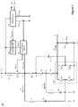
- FIG. 1 illustrates an embodiment of a switched-capacitor converter (SCC) 100 that limits current flow during a start-up phase.
- the illustrated SCC 100 down-converts the voltage V IN provided at an input 110 by a factor of four to provide a voltage V OUT at an output 120.
- the down-converted voltage V OUT provided at the output 120 is typically an intermediate voltage, within a system, that must be stepped down further before being supplied to a load such as, e.g., a memory, a central processing unit (CPU).
- a switching DC/DC converter or a linear regulator coupled to the SCC output 120 may provide this further step-down in voltage, and also provide regulation that is not provided by the SCC 100.
- the down-converted voltage V OUT provided by the SCC 100 may be used directly by a load.
- the illustrated SCC 100 includes first and second switches Q 1 , Q 2 , which are part of a first switch stage, and third and fourth switches Q 3 , Q 4 , which are part of a second switch stage.
- a rectifier 140 is interposed between the fourth switch Q 4 and ground, and provides a rectified voltage V OUT across a filter capacitor C OUT at the output 120.
- the illustrated rectifier 140 includes switches Q 7 and Q 8 , which form a first half-bridge rectifier branch, and switches Q 9 and Q 10 , which form a second half-bridge rectifier branch.
- An output current I OUT is provided by the rectifier 140 to the filter capacitor C OUT and the output 120.
- the SCC 100 further includes a first leg 130 that couples the node V 1 connecting the first and second switches Q 1 , Q 2 to the rectifier 140, and a second leg 132 that couples the node V 3 connecting the third and fourth switches Q 3 , Q 4 to the rectifier 140.
- the first leg 130 includes a first capacitor C 1 and a first inductor L 1 , and has a current I C1 flowing through it.
- the second leg 132 is similarly configured to include a second capacitor C 2 and a second inductor L 2 , and has a current I C2 flowing through it.
- the inductors L 1 , L 2 within the SCC 100 form, in combination with the capacitors C 1 , C 2 , resonant tanks which enable soft-switching of the switches if the switching is performed at a corresponding resonant frequency.
- the inductors L 1 , L 2 may be omitted in SCC circuits that are not attempting to achieve such soft-switching.
- the SCC 100 additionally includes a flying capacitor C FLY1 , which couples the node V 2 connecting the second and third switches Q 2 , Q 3 to the rectifier 140.
- the switches within the switch stages and the rectifier 140 may be partitioned into two groups, termed group A and group B herein.
- group A and group B For the illustrated SCC 100, switches Q 1 , Q 3 , Q 7 , and Q 10 are in group A, whereas switches Q 2 , Q 4 , Q 8 , and Q 9 are in group B.
- the switches of group A are switched together, and the switches of group B are switched together.
- the switching of the group A switches alternates with the switching of the group B switches.
- the group A switches are enabled so as to charge the capacitors C 1 , C 2 within the first and second legs, while discharging the flying capacitor C FLY1 .
- the capacitor C 1 is charged from the input 110 via the first switch Q 1 , and the capacitor C 2 is charged from the flying capacitor C FLY1 via the third switch Q 3 .
- the flying capacitor C FLY1 is charged, and the first and second capacitors C 1 , C 2 are discharged.
- the flying capacitor C FLY1 is charged from the capacitor C 1 via the second switch Q 2 , and the capacitor C 2 is discharged to the filter capacitor C OUT and the output 120 via the fourth switch Q 4 .
- the switches Q 1 ,...Q 4 , Q 7 ,...Q 10 illustrated in the SCC 100 of Figure 1 are power metal-oxide semiconductor field-effect transistors (MOSFETs), but other switch types may be used.
- MOSFETs power metal-oxide semiconductor field-effect transistors
- junction field-effect transistors (JFETs), bipolar junction transistors (BJTs), insulated gate bipolar transistors (IGBTs), high electron mobility transistors (HEMTs), or other types of power transistors may be preferred in some applications.
- the switches Q 1 ,...Q 4 , Q 7 ,...Q 10 may be integrated on the same semiconductor die, may each be provided on separate dies, or may otherwise be spread across a plurality of semiconductor dies.
- Each of the switches Q 1 ,...Q 4 , Q 7 ,...Q 10 within the SCC 100 has drain and source terminals, as well as a gate terminal that controls conduction between the drain and source. (For ease of illustration, these terminals are not explicitly shown in Figure 1 .)
- a control signal is provided to each of the gate terminals via a driver, which is also not shown for ease of illustration.
- the SCC 100 includes a controller 150, a voltage ramp generator 160, and a soft-start circuit 170.
- these circuits 150, 160, 170 drive a control voltage V PWM_Q1 , which is based upon a ramp voltage V RAMP , to the control terminal (e.g., gate) of the first switch Q 1 .
- V PWM_Q1 the control terminal voltage V PWM_Q1 would be referenced to whatever voltage the first switch Q1 pulls its second terminal (e.g., source) to.
- the voltage at the second terminal (voltage node V 1 ) of the first switch Q 1 would follow the input voltage V IN , minus a relatively small drain-to-source voltage drop across the first switch Q 1 .
- a sudden increase in the input voltage V IN and the resulting voltage increase at the second terminal (voltage node V 1 ) of the first switch Q 1 , would cause a sudden spike in the current I Q1 flowing into the SCC.
- the SCC 100 of Figure 1 prevents such a current spike by applying the ramp voltage V RAMP to the control terminal of the first switch Q 1 .
- the resultant voltage V SRC_RAMP at the second terminal (voltage node V 1 ) of the first switch Q 1 follows the ramp voltage V RAMP applied at the control terminal and, therefore, also rises relatively slowly, at least as compared with the rise of the input voltage V IN .
- the current flow I Q1 of the SCC 100 is determined by the voltage at the node V 1 and the effective resistance of the SCC circuitry downstream from this voltage node V 1 , i.e., the effective resistance between the voltage node V 1 and ground. This effective resistance is based upon resistances of components, e.g., capacitors, inductors, and switches, that are currently within the conduction path from the voltage node V 1 to ground.
- the voltage V SRC_RAMP at node V 1 begins at 0V and slowly ramps up until it reaches, or nearly reaches, the input voltage V IN .
- the controller 150 generates a pulse-width-modulated (PWM) control signal V PWM_QA that controls the switches Q 1 , Q 3 , Q 7 , Q 10 within group A, and a PWM control signal V PWM_QB that controls the switches Q 2 , Q 4 , Q 8 , Q 9 within group B.
- PWM control signals V PWM_QA , V PWM_QB are generated such that the switches of groups A and B are alternatively turned on, as described previously. For example, during a first phase of a switch cycle, the group A control signal V PWM_QA turns on the first switch Q 1 , while the group B control signal V PWM_QB turns off the second switch Q 2 .
- the group A control signal V PWM_QA turns off the first switch Q 1
- the group B control signal V PWM_QB turns on the second switch Q 2
- the switch control signals V PWM_QA , V PWM_QB are typically input to driver circuits for each of the switches.
- the control signal V PWM_QA may be provided to 4 separate drivers which output control signals V PWM_Q1 , V PWM_Q3 , V PWM_Q7 , V PWM_Q10 for the group A switches Q 1 , Q 3 , Q 7 , Q 10 .
- the control signal V PWM_QB may be provided to 4 other separate drivers which output control signals V PWM_Q2 , V PWM_Q4 , V PWM_Q8 , V PWM_Q9 for the group B switches Q 2 , Q 4 , Q 8 , Q 9 .
- the control signals output from the drivers are then provided to control terminals (e.g., gates) of the switches.
- control terminals e.g., gates
- the controller 150 may generate separate control signals for each of the switches, rather than providing common control signals V PWM_QA , V PWM_QB for the two switch groups, as illustrated in Figure 1 .
- the controller 150 is provided with the input voltage V IN from the SCC input 110. Upon detecting that the input voltage V IN has risen above an enable threshold indicating that an input power supply is connected to the SCC input 110, the controller 150 begins operating. This operation begins by generating an enable signal V EN_RAMP that is provided to the voltage ramp generator 160. In conjunction with or shortly after generating this enable signal V EN_RAMP , the controller 150 begins generating the switch control signals V PWM_QA , V PWM_QB as described previously. The controller 150 inputs and monitors the SCC output voltage V OUT during the start-up phase, so that the controller 150 may determine when normal steady-stage operation of the SCC may begin.
- the controller 150 may determine that steady-state operation may begin. Alternatively, the controller 150 may compare the input and output voltages V IN , V OUT and determine that steady-state operation may commence once the ratio of these voltages reaches some threshold, e.g., V IN V OUT ⁇ 4. Once the controller 150 determines that steady-state operation may commence, the controller 150 generates a power-good signal V PG , which may be used by other power converters or loads that are supplied power from the SCC 100.
- V PG power-good signal
- Detection that an input power supply has been applied to the input 110 may be performed by an input activity detector that is outside of the controller 150.
- the above-described detection may be performed directly within the voltage ramp generator 160, rather than within the controller 150.
- the input activity detector may be a circuit that is not within the controller 150 or the voltage ramp generator 160.
- the input voltage enable threshold is typically based upon an expected input voltage V IN . For example, if the expected steady-state input voltage V IN is 54V, then the input activity detection may be triggered when a measured voltage at the input 110 reaches 40V.
- the controller 150 and its constituent parts may be implemented using a combination of analog hardware components (such as transistors, amplifiers, diodes, and resistors), and processor circuitry that includes primarily digital components.
- the processor circuitry may include one or more of a digital signal processor (DSP), a general-purpose processor, and an application-specific integrated circuit (ASIC).
- DSP digital signal processor
- ASIC application-specific integrated circuit
- the controller 150 may also include memory, e.g., non-volatile memory such as flash, that includes instructions or data for use by the processor circuitry, and one or more timers, e.g., for providing the switch intervals according to the switching frequency so as to generate the switch control signals V PWM_QA , V PWM_QB .
- FIG. 2 illustrates voltage waveforms 200 within the SCC 100.
- an input power supply is connected to the SCC input 110.
- the input voltage V IN rises quickly.
- the controller 150 at time t 1 , commences start-up operation by enabling the voltage ramp generator 160 using the enable signal V EN_RAMP .
- the voltage ramp generator 160 then generates a ramped voltage (ramp voltage) V RAMP that increases from 0V to V IN over the start-up time interval from t 1 to t 2 , as illustrated.
- the output voltage V OUT is proportional to the ramped voltage V RAMP and, over this same time interval, ramps from 0V to its steady-state voltage value.
- the controller 150 detects that the output voltage V OUT has reached its steady-stage value or, alternatively, that the ratio of the input voltage V IN to the output voltage V OUT has reached an expected down-conversion ratio. Upon such detection, the controller 150 generates a power-good signal V PG indicating that the output voltage V OUT is stable, and steady-state operation of the SCC 100 begins.
- the soft-start circuit 170 of Figure 1 inputs the group A control signal V PWM_QA and outputs a first driven control signal V PWM_Q1 that controls the first switch Q 1 .
- the soft-start circuit 170 additionally inputs the ramp voltage V RAMP generated by the voltage ramp generator 160 and uses it as a reference voltage in the generation of the first driven control signal V PWM_Q1 .
- This first driven control signal V PWM_Q1 based upon the ramp voltage V RAMP , is applied to the control terminal (e.g., gate) of the first switch Q 1 . As explained above, this leads to a reduced voltage V SRC_RAMP (as compared to the input voltage V IN ) at the voltage node V 1 during the start-up phase, which serves to limit the current I Q1 flowing through the SCC 100.
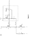
- Figure 3 illustrates an example 100A of a soft-start circuit 170, together with relevant portions of the circuitry within the SCC 100.
- the first and second switches Q 1 , Q 2 of Figure 3 are MOSFETs.
- the first terminal of each of these switches is a drain (D)
- the second terminal is a source (S)
- the control terminal is a gate (G), as illustrated.
- the soft-start circuit 170 includes a driver 172, a soft-start switch Q 1A , and a diode D 1 .
- the driver 172 inputs the group A PWM control signal V PWM_QA and outputs a first driven control signal V PWM_Q1 having appropriate voltages for controlling the soft-start switch Q 1A and the first switch Q 1 .
- the driver 172 is powered by a supply voltage V DRV_SUPPLY and has a reference voltage that is coupled to the source of the soft-start switch Q 1A and, via the diode D 1 when the first and soft-start switches Q 1 , Q 1A are turned off, to the source of the first switch Q 1 .
- the driver supply voltage V DRV_SUPPLY is +5V relative to the driver reference, such that the driver 172 provides a PWM output alternating between 0V and 5V, relative to the driver reference.
- the output of the driver 172 is coupled to the control terminals (gates) of the soft-start switch Q 1A and the first switch Q 1 .
- the ramp voltage V RAMP that is input to the soft-start circuit 170 leads to a ramp voltage V SRC_RAMP at the voltage node V 1 .
- the resultant ramp voltage V SRC_RAMP at the second terminal (e.g., source) of the first switch Q 1 (voltage node V 1 ) serves to limit the current flow through the SCC 100.
- the soft-start switch Q 1A is illustrated as a MOSFET, but other types of switches may be preferred in some applications. Note that the soft-start switch Q 1A is not required to support high current levels, as are the other switches (e.g., Q 1 , ... Q 4 ) of the SCC 100, and, hence, does not need to be a power switch.
- the diode D 1 of the soft-start circuit 170 serves to decouple the voltage reference (ground) of the driver 172 from the second terminal (e.g., source) of the first switch Q 1 when the first switch Q 1 is turned on and the driver reference voltage is connected to the ramp voltage V RAMP by the soft-start switch Q 1A .
- the voltage at the second terminal (e.g., source) of the first switch Q 1 is determined by the first driven control signal V PWM_Q1 voltage less the gate-to-source voltage V gs_Q1 of the first switch Q 1 , which will be a switch threshold voltage V THR .
- V SRC_RAMP V RAMP + V DRV_SUPPLY - V THR at the second terminal (e.g., source) of the first switch Q 1 .
- V SRC_RAMP V RAMP + V DRV_SUPPLY - V THR at the second terminal (e.g., source) of the first switch Q 1 .
- V SRC_RAMP V RAMP + 2V.
- the diode D 1 With a voltage of V RAMP on its anode side, the diode D 1 is reverse-biased such that no current flows through the diode D 1 , thereby leading to the above-mentioned decoupling of the voltage reference (ground) of the driver 172 from the second terminal (e.g., source) of the first switch Q 1 .
- the soft-start switch Q 1A is turned off such that the driver reference voltage is no longer coupled to V RAMP .
- the diode D 1 now serves to couple the driver reference voltage to the second terminal (e.g., source) of the first switch Q 1 .
- the voltage at the node V 1 will be pulled down by the current flowing to and charging the flying capacitor C FLY1 .
- the diode D 1 prevents any voltage variations at the node V 1 from producing a voltage (e.g., V gs_Q1 ) that would enable the first switch Q 1 .
- the diode D 1 connects the driver reference voltage to either the ramp voltage V RAMP or to the source voltage node V 1 , as needed. Note that the diode D 1 could be replaced with an appropriately controlled switch.
- the switches Q 1 ,...Q 4 , Q 7 ,...Q 10 may be power MOSFETs. Note that during the start-up phase, the drain-to-source voltage V ds_Q1 across the first switch Q 1 is large and this MOSFET is operating in its saturation region. For example, if the input voltage V IN is 54V and the voltage ramp V SRC_RAMP is beginning at 2V, then the first switch must drop 52V across its drain and source terminals. Hence, the first switch Q 1 should be chosen such that its breakdown voltage is higher than the expected maximum input voltage V IN .
- the first switch Q 1 must also be sized such that it can support the power dissipation required during the start-up phase of the SCC 100, i.e., I Q1 *V ds_Q1 . Because the current I Q1 is based upon the ramp voltage V RAMP , the power dissipation of the first switch Q 1 is a function of the slope of the ramp voltage V RAMP . For a first switch Q 1 having a given power rating, a slope of the ramp voltage V RAMP should be set to ensure the power rating is not exceeded.
- FIG. 4A illustrates a voltage ramp generator 460 based upon an analog resistor-capacitor (RC) network.
- the ramp enable signal V EN_RAMP as generated by the controller 150 upon detecting that an input voltage V IN is available, turns on a ramp switch Q RAMP , so as to apply the input voltage V IN to an RC network consisting of a resistor R RAMP and a capacitor C RAMP .
- a voltage at a node V RC connecting the resistor R RAMP and the capacitor CRAMP increases exponentially from 0V beginning when the voltage V IN is applied.
- An amplifier 462 serves to buffer and amplify the voltage at the node V RC , and outputs the ramp voltage V RAMP .
- the voltage at the node V RC rises exponentially and approaches the input voltage V IN . Without modification, the voltage at the node V RC will not fully reach the input voltage V IN , as desired.
- the amplifier 462 also serves to isolate the RC network from the soft-start circuit 170, such that the impedance of the soft-start circuit 170 does not affect the ramp voltage V RAMP provided by the RC network.
- the corresponding output voltage V RAMP is determined by this time constant ⁇ and the gain A of the amplifier 462.
- the voltage ramp generator 460 of Figure 4A has the advantage that it is fairly simple and that the required circuitry is minimal.
- FIG. 5A illustrates a voltage ramp generator 560 based upon a current source.
- the ramp enable signal V EN_RAMP as generated by the controller 150 upon detecting that an input voltage V IN is available, provides a voltage that enables a current source circuit comprised of a first voltage ramp switch Q VR1 , a resistor R2, a resistor R4 and a Zener diode D1.
- the first voltage ramp switch Q VR1 is an NPN bipolar junction transistor (BJT) having collector, emitter, and base (control) terminals.
- a current I1 flowing into the collector terminal of the first voltage ramp switch Q VR1 is based on the resistance of R4, together with the electrical characteristics of the first voltage ramp switch Q VR1 and the Zener diode D1.
- a Zener voltage (reverse breakdown voltage) of the Zener diode provides a highly stable voltage that is provided across the base-to-emitter junction of the switch Q VR1 and the resistor R4. This highly-stable voltage, in turn, leads to a fairly constant current I1 being drawn by the switch Q VR1 .
- the current I1 is drawn through a current mirror comprised of second and third voltage ramp switches Q VR2 , Q VR3 , which are PNP BJTs in the illustrated voltage ramp generator 560.
- the current mirror serves to isolate the current source from any circuitry connected to the voltage ramp generator 560, such that the current source is not affected by the impedance of other circuitry, and vice versa.
- a second current I2 mirrors the first current I1, and the second current I2 should also be relatively constant.
- a resistor R3 and a fourth voltage ramp switch O VR4 which is driven by an inverter 562, serve to discharge the capacitor C1 when the ramp enable signal V EN_RAMP is inactive. This ensures that the voltage at V RAMP begins at zero when the voltage ramp generator is activated.
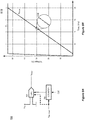
- FIG. 5B illustrates waveforms 500B corresponding to the ramp voltage V RAMP for different values of the resistor R4.
- Figure 6A illustrates a voltage ramp generator 660 based upon a digital-to-analog converter (DAC) 662.
- the ramp enable signal V EN_RAMP as generated by the controller 150 upon detecting that an input voltage V IN is available, enables a counter 664 and, in some implementations, the DAC 662.
- the counter 664 then begins counting from 0 to some maximum value, at which point the counting stops. For example, an 8-bit counter would count from 0 to 255.
- the count is incremented upon each cycle of an input clock (CLK).
- the count is output from the counter 664 and input to the DAC 662.
- the DAC 662 outputs a voltage V RAMP based upon the count.
- the DAC 662 is supplied with the input voltage V IN .
- the counter 664 may be disabled, e.g., to save power, or the counter 664 may simply maintain the maximum output count value.
- the output voltage V RAMP from the DAC 662 may be latched to the input voltage V IN , so that the DAC 662 may be disabled to save power
- Figure 6B illustrates waveforms 600B for the ramp voltage V RAMP as output from the voltage ramp generator 660. Note that the ramp voltage V RAMP appears highly linear, unlike the voltage produced by the voltage ramp generator 460 based upon an RC network. An expanded view 610B of the V RAMP waveform shows that it has a staircase shape, wherein each step corresponds to an increase due to an increment in the count.
- the ramp voltage V RAMP could be controlled in a more dynamic way.
- the controller 150 could measure the voltage V ds_Q1 across and the current I Q1 through the first switch Q 1 , and adjust the ramping of the ramp voltage V RAMP to ensure power dissipation requirements of the first switch Q 1 are being met.
- the voltage ramp generator 160 is shown as a separate circuit within the SCC 100 of Figure 1 , the voltage ramp generator may be included with a controller of the SCC 100.
- the largely digital DAC-based voltage ramp generator 660 of Figure 6A is particularly amenable to inclusion within a controller such as the controller 150 of Figure 1 .
- the slope of the generated voltage ramp V RAMP must be chosen to ensure that the current is adequately limited for the SCC 100.
- a slow ramp voltage V RAMP yields slowly-increasing current and decreases the electrical stress on the switches and capacitors within the SCC 100, but comes at the expense of an undesired lengthy start-up phase.
- the slope of the ramp voltage V RAMP must be chosen to meet maximum current requirements for the components of the SCC 100, and to keep the start-up time of the SCC 100 reasonably short.
- the soft-starting of an SCC has been described in the context of the SCC 100 of Figure 1 , which down-converts the input voltage V IN by a factor of 4 and includes resonant inductors in its legs.
- the soft-start circuitry including the voltage ramp generator 160 and the soft-start circuit 170, may be similarly applied to other SCC topologies.
- the ramp voltage V RAMP is similarly generated and applied to the control terminal (e.g., gate) of the first power switch within an SCC, wherein the first power switch is coupled to an input power supply.
- Figure 7 illustrates a 2:1 SCC 700 having no resonant inductors.
- the inductors L 1 , L 2 , the capacitors C 2 , C FLY1 corresponding to the second switch stage, the switches Q 3 , Q 4 of the second switch stage, and the switches Q 9 , Q 10 of the second rectifier branch are deleted. Otherwise, the circuitry and control of the SCC 700 are largely the same as that of the SCC 100 of Figure 1 .
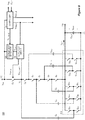
- Figure 8 illustrates a 6:1 SCC 800 having additional rectifier branches within its rectifier 840.
- the SCC 800 includes an additional switch stage that has fifth and sixth switches Q 5 , Q 6 .
- An additional capacitor C 3 and an additional flying capacitor C FLY2 are also included and couple the additional switch stage to the rectifier 840.
- the rectifier 840 of Figure 8 includes rectifier branches dedicated to each of the legs of the SCC 800, rather than using a common rectifier branch to support multiple legs as in the SCC 100 of Figure 1 .
- FIG 9 illustrates a method 900 for soft-starting a switched-capacitor converter (SCC) such as that illustrated in Figure 1 .
- This method may be implemented within an SCC that converts power provided at an input into power at an output.
- Such an SCC includes a rectifier at the output and a first switch stage that is interposed between the input and the rectifier.
- the first switch stage comprises a first and a second switch connected in series, wherein the first switch has a first terminal that is coupled to the input, a second terminal that is coupled to the second switch, and a control terminal.
- a first capacitor couples the first switch stage to the rectifier.
- a voltage V IN at the input is measured 910.
- This input voltage V IN is compared 920 against an input voltage threshold V IN_THRESH that indicates whether the input voltage V IN is adequate for commencing operation of the SCC.
- V IN_THRESH an input voltage threshold
- generation of a ramp voltage is started 930 and applied to the control terminal of the first switch.
- switch control signals e.g., PWM waveforms, are generated 940 for the switches within the SCC.
- steps 930, 940 could be swapped in order, but typically are executed at the same time.
- Such operation including the ramping of the voltage applied to the first switch, continues until the output voltage V OUT is sufficient to maintain steady-state operation of the SCC.
- This determination is made by measuring 950 the output voltage V OUT and comparing 960 it against an output voltage threshold V OUT_THRESH .
- the ratio of the input voltage V IN to the output voltage V OUT may be compared against the expected down-conversion ratio of the SCC (e.g., 4 for the SCC 100 of Figure 1 ).
- a switched-capacitor converter comprising: an input for coupling to an input power supply; an output for providing power to a load; a first switch stage comprising a first switch and a second switch connected in series and interposed between the input and the output, the first switch comprising a first terminal that is coupled to the input, a second terminal that is coupled to the second switch, and a control terminal; a first capacitor which couples the first switch stage to the output; a controller operable to generate a first control signal for controlling the first switch and a second control signal for controlling the second switch, such that the first and second switches are alternately switched; an input activation detector operable to generate an input activation signal based upon an input voltage at the input, wherein the input activation signal indicates that power is being supplied at the input; a voltage ramp generator operable to generate a ramped voltage responsive to receiving the input activation signal, wherein the ramped voltage increases from a minimum ramp voltage to a maximum ramp voltage, and the voltage ramp generator limits a slope of the ramped voltage to be
- Example 2 The switched-capacitor converter of example 1, further comprising: a rectifier at the output.
- Example 3 The switched-capacitor converter of example 1, wherein the soft-start circuit comprises a soft-start switch having a first soft-start terminal coupled to the ramped voltage, a second soft-start terminal that provides a switch control reference voltage for the first switch, and a soft-start control terminal.
- the soft-start circuit comprises a soft-start switch having a first soft-start terminal coupled to the ramped voltage, a second soft-start terminal that provides a switch control reference voltage for the first switch, and a soft-start control terminal.
- Example 4 The switched-capacitor converter of example 3, wherein the soft-start switch is controlled by the first control signal which also controls the first switch.
- Example 5 The switched-capacitor converter of example 3, further comprising: a first gate driver that inputs the first control signal and outputs a first driven control signal that is coupled to the first control terminal of the first switch and the first soft-start control terminal, wherein the first driven control signal provides a sufficient voltage for turning on the first switch and the first soft-start switch when the first control signal provides an active signal level.
- Example 6 The switched-capacitor converter of example 3, wherein the soft-start circuit further comprises a soft-start diode that couples the second soft-start terminal to the second terminal of the second switch.
- Example 7 The switched-capacitor converter of example 1, wherein the voltage ramp generator is coupled to the input and the ramped voltage is based upon the input voltage.
- Example 8 The switched-capacitor converter of example 7, wherein the maximum ramp voltage generated by the voltage ramp generator is the input voltage once the input voltage is active and has reached a steady-state voltage level.
- Example 9 The switched-capacitor converter of example 1, wherein the voltage ramp generator comprises a resistor and a capacitor, and the slope of the ramped voltage is based upon a resistance of the resistor and a capacitance of the capacitor.
- Example 10 The switched-capacitor converter of example 1, wherein the voltage ramp generator comprises a digital-to-analog converter (DAC) which provides the ramped voltage, wherein the DAC periodically increases the ramped voltage until the ramped voltage reaches the maximum ramp voltage.
- DAC digital-to-analog converter
- Example 11 The switched-capacitor converter of example 10, wherein the maximum ramp voltage is the same as the input voltage once the input voltage is active and has reached a steady-state voltage level.
- Example 12 The switched-capacitor converter of example 1, wherein during a ramp-up interval when the ramped voltage increases from the minimum ramp voltage to the maximum ramp voltage, the ramped voltage at a given instant of time determines a current flowing through the first switch at that given instant of time.
- Example 13 The switched-capacitor converter of example 1, wherein the minimum ramp voltage is zero.
- Example 14 The switched-capacitor converter of example 1, wherein the controller includes the input activity detector, and the input activation signal is generated responsive to detecting that the input voltage is above an input activity threshold voltage.
- Example 15 The switched-capacitor converter of example 1, wherein the controller senses the input voltage and an output voltage at the output, and enables power to an output load in response to detecting that a ratio of the sensed input voltage to the sensed output voltage has reached a down-conversion ratio of the switched-capacitor converter.
- Example 16 The switched-capacitor converter of example 1, further comprising: a first inductor connected in series with the first capacitor, such that the serially-connected first inductor and first capacitor couple the first switch stage to the output.
- Example 17 The switched-capacitor converter of example 1, wherein the first switch stage is directly coupled to the output, and the switched-capacitor converter down-converts the input voltage by a factor of two.
- Example 18 The switched-capacitor converter of example 1, further comprising: a second switch stage comprising a third switch and a fourth switch connected in series and interposed between the first switch stage and the output, wherein the third switch is controlled by the first control signal and the fourth switch is controlled by the second control signal; and a second capacitor which couples the second switch stage to the output.
- Example 19 The switched-capacitor converter of example 1, wherein the first switch is a power metal-oxide semiconductor field-effect transistor (MOSFET), and wherein the first terminal is a drain, the second terminal is a source, and the control terminal is a gate.
- MOSFET power metal-oxide semiconductor field-effect transistor
- Example 20 A method for limiting a current within a switched-capacitor converter (SCC) at its start-up, the SCC comprising an input, an output, a first switch stage comprising a first switch and a second switch connected in series and interposed between the input and the output, the first switch comprising a first terminal that is coupled to the input, a second terminal that is coupled to the second switch, and a control terminal, and a first capacitor interposed between the first switch stage to the output, the method comprising: detecting that an input voltage at the input has risen above an activation threshold which indicates that the input is supplying power to the SCC; responsive to the detecting, generating a ramp voltage having a slope that is less than a slope of the input voltage as it rises during activation of the input; setting a voltage at the second terminal of the first switch based upon the ramp voltage.
- SCC switched-capacitor converter
- Example 21 The method of example 20, wherein the ramp voltage increases to a maximum voltage that is the same as the input voltage when the input voltage has reached a steady-state voltage level.
- Example 22 The method of example 20, wherein the ramp generator further comprises a digital to analog converter (DAC), the method further comprising: incrementing a counter that is coupled to the DAC; and updating an output of the DAC and providing the DAC output as the ramped voltage.
- DAC digital to analog converter
Landscapes
- Engineering & Computer Science (AREA)
- Power Engineering (AREA)
- Dc-Dc Converters (AREA)
Applications Claiming Priority (1)
| Application Number | Priority Date | Filing Date | Title |
|---|---|---|---|
| US15/875,790 US10199928B1 (en) | 2018-01-19 | 2018-01-19 | Soft start of switched capacitor converters by reducing voltage provided by initial power switch |
Publications (3)
| Publication Number | Publication Date |
|---|---|
| EP3514932A2 true EP3514932A2 (de) | 2019-07-24 |
| EP3514932A3 EP3514932A3 (de) | 2019-07-31 |
| EP3514932B1 EP3514932B1 (de) | 2021-08-25 |
Family
ID=65036692
Family Applications (1)
| Application Number | Title | Priority Date | Filing Date |
|---|---|---|---|
| EP19152330.7A Active EP3514932B1 (de) | 2018-01-19 | 2019-01-17 | Sanftanlauf von schaltkondensatorwandlern |
Country Status (3)
| Country | Link |
|---|---|
| US (2) | US10199928B1 (de) |
| EP (1) | EP3514932B1 (de) |
| CN (1) | CN110061617B (de) |
Cited By (1)
| Publication number | Priority date | Publication date | Assignee | Title |
|---|---|---|---|---|
| EP3849069A1 (de) * | 2020-01-08 | 2021-07-14 | Infineon Technologies Austria AG | Inbetriebnahme eines spannungswandlers |
Families Citing this family (17)
| Publication number | Priority date | Publication date | Assignee | Title |
|---|---|---|---|---|
| US10784777B2 (en) * | 2017-12-28 | 2020-09-22 | Texas Instruments Incorporated | Output current boosting of capacitor-drop power supplies |
| WO2019196064A1 (zh) * | 2018-04-12 | 2019-10-17 | 深圳市汇顶科技股份有限公司 | 电荷帮浦电路及其控制方法 |
| US12051972B2 (en) * | 2019-05-23 | 2024-07-30 | Infineon Technologies Austria Ag | Hybrid resonant power supply |
| CN110492735B (zh) * | 2019-09-11 | 2021-06-01 | 上海南芯半导体科技有限公司 | 电荷泵的电容自检查和软启电电路及其实现方法 |
| CN110557012B (zh) * | 2019-09-11 | 2020-07-17 | 上海南芯半导体科技有限公司 | 用于2:1正向电荷泵的驱动电路及其实现方法 |
| US11462916B2 (en) * | 2019-11-01 | 2022-10-04 | Hamilton Sundstrand Corporation | Capacitor pre-charging circuits |
| TWI711262B (zh) * | 2019-12-13 | 2020-11-21 | 東元電機股份有限公司 | 變頻器裝置以及依據輸出電壓值而選擇性輸出電流之方法 |
| CN113131730B (zh) * | 2019-12-30 | 2023-12-19 | 台达电子工业股份有限公司 | 预充电控制电路及其控制方法 |
| CN113300603B (zh) * | 2020-02-21 | 2024-10-08 | 台达电子工业股份有限公司 | 电源转换系统 |
| CN111736686B (zh) * | 2020-06-12 | 2023-04-11 | 苏州浪潮智能科技有限公司 | 一种异常开启scc电路的保护电路及服务器 |
| TWI740619B (zh) * | 2020-08-21 | 2021-09-21 | 國立臺灣科技大學 | 用於電源轉換器的控制電路及控制方法 |
| EP4246790B1 (de) * | 2021-01-28 | 2026-01-28 | Huawei Digital Power Technologies Co., Ltd. | Wandlerschaltung, vorladesteuerungsverfahren für die wandlerschaltung und fotovoltaisches system |
| CN114915174B (zh) * | 2021-02-09 | 2025-07-29 | 台达电子企业管理(上海)有限公司 | 非隔离混合式谐振电路 |
| CN113644820B (zh) * | 2021-08-24 | 2025-07-22 | 南京能利芯科技有限公司 | 具有全波输出整流的多相开关电容谐振腔转换电路的电源转换拓扑及基于其的电源转换结构 |
| CN113839554B (zh) * | 2021-10-28 | 2024-08-13 | 阳光电源股份有限公司 | 一种开关电容变换器及其预充电方法 |
| US12294299B2 (en) * | 2022-04-11 | 2025-05-06 | Hamilton Sundstrand Corporation | Soft start for buck converters |
| US12095358B2 (en) * | 2022-04-12 | 2024-09-17 | Reed Semiconductor Corporation | Internal ramp voltage generator for the soft start of DC-DC converter |
Family Cites Families (19)
| Publication number | Priority date | Publication date | Assignee | Title |
|---|---|---|---|---|
| US6933710B2 (en) * | 2002-02-19 | 2005-08-23 | Fairchild Semiconductor Corporation | Soft start techniques for control loops that regulate DC/DC converters |
| US7038514B2 (en) * | 2003-10-28 | 2006-05-02 | Intersil Americas Inc. | Startup circuit for a DC-DC converter |
| US7378827B2 (en) * | 2005-08-24 | 2008-05-27 | Micrel, Incorporated | Analog internal soft-start and clamp circuit for switching regulator |
| ATE501545T1 (de) * | 2007-08-20 | 2011-03-15 | Austriamicrosystems Ag | Gleichstromwandleranordnung und verfahren zur gleichstromwandlung |
| US7616457B2 (en) * | 2007-11-20 | 2009-11-10 | System General Corp. | Synchronous regulation circuit |
| US8890501B2 (en) * | 2011-02-11 | 2014-11-18 | Intersil Americas, Llc | System and method for soft-starting a power converter with a pre-charged output |
| US9081398B2 (en) * | 2012-03-23 | 2015-07-14 | Fairchild Semiconductor Corporation | Adaptive startup control for boost converter |
| CN102684479B (zh) | 2012-05-09 | 2014-10-29 | 成都芯源系统有限公司 | 电荷泵式分压电路及其启动方法 |
| CN103475223A (zh) * | 2012-06-08 | 2013-12-25 | 中国科学院深圳先进技术研究院 | 降压型转换器 |
| US10014823B2 (en) * | 2012-08-05 | 2018-07-03 | Ben-Gurion University Of The Negev Research & Development Authority | High efficiency resonant switched capacitor converter with continuous conversion ratio |
| US8503203B1 (en) | 2012-10-16 | 2013-08-06 | Arctic Sand Technologies, Inc. | Pre-charge of switched capacitor circuits with cascoded drivers |
| US9847712B2 (en) * | 2013-03-15 | 2017-12-19 | Peregrine Semiconductor Corporation | Fault control for switched capacitor power converter |
| US9203299B2 (en) * | 2013-03-15 | 2015-12-01 | Artic Sand Technologies, Inc. | Controller-driven reconfiguration of switched-capacitor power converter |
| US9042127B2 (en) * | 2013-03-15 | 2015-05-26 | Infineon Technologies Austria Ag | LED power supply |
| US9653986B2 (en) | 2013-03-15 | 2017-05-16 | Maxim Integrated Products, Inc. | Multi-level step-up converter topologies, control and soft start systems and methods |
| US9484799B2 (en) * | 2014-01-17 | 2016-11-01 | Linear Technology Corporation | Switched capacitor DC-DC converter with reduced in-rush current and fault protection |
| US9484800B2 (en) * | 2014-03-05 | 2016-11-01 | Tower Semiconductor Ltd. | Soft-start circuit for switching regulator |
| CN109478842B (zh) | 2016-07-15 | 2022-10-21 | 亚德诺半导体国际无限责任公司 | 电荷泵的平衡技术和电路 |
| US9917517B1 (en) * | 2016-10-26 | 2018-03-13 | Google Inc. | Switched tank converter |
-
2018
- 2018-01-19 US US15/875,790 patent/US10199928B1/en active Active
- 2018-12-27 US US16/234,060 patent/US10491111B2/en active Active
-
2019
- 2019-01-08 CN CN201910016546.9A patent/CN110061617B/zh active Active
- 2019-01-17 EP EP19152330.7A patent/EP3514932B1/de active Active
Non-Patent Citations (1)
| Title |
|---|
| None |
Cited By (2)
| Publication number | Priority date | Publication date | Assignee | Title |
|---|---|---|---|---|
| EP3849069A1 (de) * | 2020-01-08 | 2021-07-14 | Infineon Technologies Austria AG | Inbetriebnahme eines spannungswandlers |
| US11502597B2 (en) | 2020-01-08 | 2022-11-15 | Infineon Technologies Austria Ag | Startup of a voltage converter |
Also Published As
| Publication number | Publication date |
|---|---|
| EP3514932B1 (de) | 2021-08-25 |
| CN110061617B (zh) | 2024-04-26 |
| US10199928B1 (en) | 2019-02-05 |
| EP3514932A3 (de) | 2019-07-31 |
| US20190229613A1 (en) | 2019-07-25 |
| CN110061617A (zh) | 2019-07-26 |
| US10491111B2 (en) | 2019-11-26 |
Similar Documents
| Publication | Publication Date | Title |
|---|---|---|
| EP3514932B1 (de) | Sanftanlauf von schaltkondensatorwandlern | |
| US10666135B2 (en) | Balancing charge pump circuits | |
| US9391516B2 (en) | Switching charger, the control circuit and the control method thereof | |
| US9998012B2 (en) | Voltage peak detection circuit and detection method | |
| US9882485B2 (en) | Current metering for transitioning between operating modes in switching regulators | |
| US9083246B2 (en) | Control circuit for primary side control of switching power supply | |
| US7298124B2 (en) | PWM regulator with discontinuous mode and method therefor | |
| US9054596B2 (en) | Device for synchronous DC-DC conversion and synchronous DC-DC converter | |
| US20120146606A1 (en) | Constant On-Time Converter with Stabilizing Operation and Method Thereof | |
| US10826392B2 (en) | Voltage regulator with an adaptive off-time generator | |
| US9431845B2 (en) | Switching charger, the control circuit and the control method thereof | |
| US9684320B2 (en) | DC-DC converter and method for controlling the same and power supply of energy storage system including the same DC-DC converter | |
| US8330440B2 (en) | Power supply device with gain changing error amplifier | |
| US7158394B2 (en) | Switching power supply circuit with a soft-start function | |
| EP0529391A1 (de) | Spannungswandler | |
| US20100033145A1 (en) | DCR sense for a COT power converter | |
| US9042135B2 (en) | Methods and apparatuses for a soft-start function with auto-disable | |
| CN112751480A (zh) | 切换调节器控制 | |
| CN111464029B (zh) | 用于dc-dc转换器的电流感测控制器 | |
| US20240405657A1 (en) | Feedback circuit with adjustable loop gain for a boost converter | |
| CN111316547A (zh) | 降压-升压电力转换器控制器 | |
| US12362675B2 (en) | Integrated circuit and power supply circuit | |
| US11955880B2 (en) | Overcurrent protection circuit, power supply control device, inverting type switching power supply | |
| JP4950254B2 (ja) | スイッチング電源装置 | |
| WO2012082106A1 (en) | Method of forming a low power dissipation regulator and structure therefor |
Legal Events
| Date | Code | Title | Description |
|---|---|---|---|
| PUAI | Public reference made under article 153(3) epc to a published international application that has entered the european phase |
Free format text: ORIGINAL CODE: 0009012 |
|
| STAA | Information on the status of an ep patent application or granted ep patent |
Free format text: STATUS: THE APPLICATION HAS BEEN PUBLISHED |
|
| PUAL | Search report despatched |
Free format text: ORIGINAL CODE: 0009013 |
|
| AK | Designated contracting states |
Kind code of ref document: A2 Designated state(s): AL AT BE BG CH CY CZ DE DK EE ES FI FR GB GR HR HU IE IS IT LI LT LU LV MC MK MT NL NO PL PT RO RS SE SI SK SM TR |
|
| AX | Request for extension of the european patent |
Extension state: BA ME |
|
| AK | Designated contracting states |
Kind code of ref document: A3 Designated state(s): AL AT BE BG CH CY CZ DE DK EE ES FI FR GB GR HR HU IE IS IT LI LT LU LV MC MK MT NL NO PL PT RO RS SE SI SK SM TR |
|
| AX | Request for extension of the european patent |
Extension state: BA ME |
|
| RIC1 | Information provided on ipc code assigned before grant |
Ipc: H02M 3/07 20060101AFI20190621BHEP Ipc: H02M 1/36 20070101ALI20190621BHEP Ipc: H02M 1/32 20070101ALI20190621BHEP |
|
| STAA | Information on the status of an ep patent application or granted ep patent |
Free format text: STATUS: REQUEST FOR EXAMINATION WAS MADE |
|
| STAA | Information on the status of an ep patent application or granted ep patent |
Free format text: STATUS: EXAMINATION IS IN PROGRESS |
|
| 17P | Request for examination filed |
Effective date: 20200131 |
|
| RBV | Designated contracting states (corrected) |
Designated state(s): AL AT BE BG CH CY CZ DE DK EE ES FI FR GB GR HR HU IE IS IT LI LT LU LV MC MK MT NL NO PL PT RO RS SE SI SK SM TR |
|
| 17Q | First examination report despatched |
Effective date: 20200226 |
|
| GRAP | Despatch of communication of intention to grant a patent |
Free format text: ORIGINAL CODE: EPIDOSNIGR1 |
|
| STAA | Information on the status of an ep patent application or granted ep patent |
Free format text: STATUS: GRANT OF PATENT IS INTENDED |
|
| INTG | Intention to grant announced |
Effective date: 20210319 |
|
| RIC1 | Information provided on ipc code assigned before grant |
Ipc: H02H 9/00 20060101ALI20210305BHEP Ipc: H02M 1/36 20070101ALI20210305BHEP Ipc: H02M 1/32 20070101ALI20210305BHEP Ipc: H02M 3/07 20060101AFI20210305BHEP |
|
| GRAS | Grant fee paid |
Free format text: ORIGINAL CODE: EPIDOSNIGR3 |
|
| GRAA | (expected) grant |
Free format text: ORIGINAL CODE: 0009210 |
|
| STAA | Information on the status of an ep patent application or granted ep patent |
Free format text: STATUS: THE PATENT HAS BEEN GRANTED |
|
| AK | Designated contracting states |
Kind code of ref document: B1 Designated state(s): AL AT BE BG CH CY CZ DE DK EE ES FI FR GB GR HR HU IE IS IT LI LT LU LV MC MK MT NL NO PL PT RO RS SE SI SK SM TR |
|
| REG | Reference to a national code |
Ref country code: CH Ref legal event code: EP |
|
| REG | Reference to a national code |
Ref country code: IE Ref legal event code: FG4D Ref country code: AT Ref legal event code: REF Ref document number: 1424816 Country of ref document: AT Kind code of ref document: T Effective date: 20210915 |
|
| REG | Reference to a national code |
Ref country code: DE Ref legal event code: R096 Ref document number: 602019007030 Country of ref document: DE |
|
| REG | Reference to a national code |
Ref country code: LT Ref legal event code: MG9D |
|
| REG | Reference to a national code |
Ref country code: NL Ref legal event code: MP Effective date: 20210825 |
|
| REG | Reference to a national code |
Ref country code: AT Ref legal event code: MK05 Ref document number: 1424816 Country of ref document: AT Kind code of ref document: T Effective date: 20210825 |
|
| PG25 | Lapsed in a contracting state [announced via postgrant information from national office to epo] |
Ref country code: HR Free format text: LAPSE BECAUSE OF FAILURE TO SUBMIT A TRANSLATION OF THE DESCRIPTION OR TO PAY THE FEE WITHIN THE PRESCRIBED TIME-LIMIT Effective date: 20210825 Ref country code: PT Free format text: LAPSE BECAUSE OF FAILURE TO SUBMIT A TRANSLATION OF THE DESCRIPTION OR TO PAY THE FEE WITHIN THE PRESCRIBED TIME-LIMIT Effective date: 20211227 Ref country code: NO Free format text: LAPSE BECAUSE OF FAILURE TO SUBMIT A TRANSLATION OF THE DESCRIPTION OR TO PAY THE FEE WITHIN THE PRESCRIBED TIME-LIMIT Effective date: 20211125 Ref country code: LT Free format text: LAPSE BECAUSE OF FAILURE TO SUBMIT A TRANSLATION OF THE DESCRIPTION OR TO PAY THE FEE WITHIN THE PRESCRIBED TIME-LIMIT Effective date: 20210825 Ref country code: BG Free format text: LAPSE BECAUSE OF FAILURE TO SUBMIT A TRANSLATION OF THE DESCRIPTION OR TO PAY THE FEE WITHIN THE PRESCRIBED TIME-LIMIT Effective date: 20211125 Ref country code: AT Free format text: LAPSE BECAUSE OF FAILURE TO SUBMIT A TRANSLATION OF THE DESCRIPTION OR TO PAY THE FEE WITHIN THE PRESCRIBED TIME-LIMIT Effective date: 20210825 Ref country code: FI Free format text: LAPSE BECAUSE OF FAILURE TO SUBMIT A TRANSLATION OF THE DESCRIPTION OR TO PAY THE FEE WITHIN THE PRESCRIBED TIME-LIMIT Effective date: 20210825 Ref country code: ES Free format text: LAPSE BECAUSE OF FAILURE TO SUBMIT A TRANSLATION OF THE DESCRIPTION OR TO PAY THE FEE WITHIN THE PRESCRIBED TIME-LIMIT Effective date: 20210825 Ref country code: RS Free format text: LAPSE BECAUSE OF FAILURE TO SUBMIT A TRANSLATION OF THE DESCRIPTION OR TO PAY THE FEE WITHIN THE PRESCRIBED TIME-LIMIT Effective date: 20210825 Ref country code: SE Free format text: LAPSE BECAUSE OF FAILURE TO SUBMIT A TRANSLATION OF THE DESCRIPTION OR TO PAY THE FEE WITHIN THE PRESCRIBED TIME-LIMIT Effective date: 20210825 |
|
| PG25 | Lapsed in a contracting state [announced via postgrant information from national office to epo] |
Ref country code: PL Free format text: LAPSE BECAUSE OF FAILURE TO SUBMIT A TRANSLATION OF THE DESCRIPTION OR TO PAY THE FEE WITHIN THE PRESCRIBED TIME-LIMIT Effective date: 20210825 Ref country code: LV Free format text: LAPSE BECAUSE OF FAILURE TO SUBMIT A TRANSLATION OF THE DESCRIPTION OR TO PAY THE FEE WITHIN THE PRESCRIBED TIME-LIMIT Effective date: 20210825 Ref country code: GR Free format text: LAPSE BECAUSE OF FAILURE TO SUBMIT A TRANSLATION OF THE DESCRIPTION OR TO PAY THE FEE WITHIN THE PRESCRIBED TIME-LIMIT Effective date: 20211126 |
|
| PG25 | Lapsed in a contracting state [announced via postgrant information from national office to epo] |
Ref country code: NL Free format text: LAPSE BECAUSE OF FAILURE TO SUBMIT A TRANSLATION OF THE DESCRIPTION OR TO PAY THE FEE WITHIN THE PRESCRIBED TIME-LIMIT Effective date: 20210825 |
|
| PG25 | Lapsed in a contracting state [announced via postgrant information from national office to epo] |
Ref country code: DK Free format text: LAPSE BECAUSE OF FAILURE TO SUBMIT A TRANSLATION OF THE DESCRIPTION OR TO PAY THE FEE WITHIN THE PRESCRIBED TIME-LIMIT Effective date: 20210825 |
|
| REG | Reference to a national code |
Ref country code: DE Ref legal event code: R097 Ref document number: 602019007030 Country of ref document: DE |
|
| PG25 | Lapsed in a contracting state [announced via postgrant information from national office to epo] |
Ref country code: SM Free format text: LAPSE BECAUSE OF FAILURE TO SUBMIT A TRANSLATION OF THE DESCRIPTION OR TO PAY THE FEE WITHIN THE PRESCRIBED TIME-LIMIT Effective date: 20210825 Ref country code: SK Free format text: LAPSE BECAUSE OF FAILURE TO SUBMIT A TRANSLATION OF THE DESCRIPTION OR TO PAY THE FEE WITHIN THE PRESCRIBED TIME-LIMIT Effective date: 20210825 Ref country code: RO Free format text: LAPSE BECAUSE OF FAILURE TO SUBMIT A TRANSLATION OF THE DESCRIPTION OR TO PAY THE FEE WITHIN THE PRESCRIBED TIME-LIMIT Effective date: 20210825 Ref country code: EE Free format text: LAPSE BECAUSE OF FAILURE TO SUBMIT A TRANSLATION OF THE DESCRIPTION OR TO PAY THE FEE WITHIN THE PRESCRIBED TIME-LIMIT Effective date: 20210825 Ref country code: CZ Free format text: LAPSE BECAUSE OF FAILURE TO SUBMIT A TRANSLATION OF THE DESCRIPTION OR TO PAY THE FEE WITHIN THE PRESCRIBED TIME-LIMIT Effective date: 20210825 Ref country code: AL Free format text: LAPSE BECAUSE OF FAILURE TO SUBMIT A TRANSLATION OF THE DESCRIPTION OR TO PAY THE FEE WITHIN THE PRESCRIBED TIME-LIMIT Effective date: 20210825 |
|
| PLBE | No opposition filed within time limit |
Free format text: ORIGINAL CODE: 0009261 |
|
| STAA | Information on the status of an ep patent application or granted ep patent |
Free format text: STATUS: NO OPPOSITION FILED WITHIN TIME LIMIT |
|
| PG25 | Lapsed in a contracting state [announced via postgrant information from national office to epo] |
Ref country code: IT Free format text: LAPSE BECAUSE OF FAILURE TO SUBMIT A TRANSLATION OF THE DESCRIPTION OR TO PAY THE FEE WITHIN THE PRESCRIBED TIME-LIMIT Effective date: 20210825 |
|
| 26N | No opposition filed |
Effective date: 20220527 |
|
| PG25 | Lapsed in a contracting state [announced via postgrant information from national office to epo] |
Ref country code: SI Free format text: LAPSE BECAUSE OF FAILURE TO SUBMIT A TRANSLATION OF THE DESCRIPTION OR TO PAY THE FEE WITHIN THE PRESCRIBED TIME-LIMIT Effective date: 20210825 Ref country code: MC Free format text: LAPSE BECAUSE OF FAILURE TO SUBMIT A TRANSLATION OF THE DESCRIPTION OR TO PAY THE FEE WITHIN THE PRESCRIBED TIME-LIMIT Effective date: 20210825 |
|
| REG | Reference to a national code |
Ref country code: CH Ref legal event code: PL |
|
| REG | Reference to a national code |
Ref country code: BE Ref legal event code: MM Effective date: 20220131 |
|
| PG25 | Lapsed in a contracting state [announced via postgrant information from national office to epo] |
Ref country code: LU Free format text: LAPSE BECAUSE OF NON-PAYMENT OF DUE FEES Effective date: 20220117 |
|
| PG25 | Lapsed in a contracting state [announced via postgrant information from national office to epo] |
Ref country code: BE Free format text: LAPSE BECAUSE OF NON-PAYMENT OF DUE FEES Effective date: 20220131 |
|
| PG25 | Lapsed in a contracting state [announced via postgrant information from national office to epo] |
Ref country code: LI Free format text: LAPSE BECAUSE OF NON-PAYMENT OF DUE FEES Effective date: 20220131 Ref country code: CH Free format text: LAPSE BECAUSE OF NON-PAYMENT OF DUE FEES Effective date: 20220131 |
|
| PG25 | Lapsed in a contracting state [announced via postgrant information from national office to epo] |
Ref country code: IE Free format text: LAPSE BECAUSE OF NON-PAYMENT OF DUE FEES Effective date: 20220117 |
|
| P01 | Opt-out of the competence of the unified patent court (upc) registered |
Effective date: 20230528 |
|
| PG25 | Lapsed in a contracting state [announced via postgrant information from national office to epo] |
Ref country code: MK Free format text: LAPSE BECAUSE OF FAILURE TO SUBMIT A TRANSLATION OF THE DESCRIPTION OR TO PAY THE FEE WITHIN THE PRESCRIBED TIME-LIMIT Effective date: 20210825 Ref country code: CY Free format text: LAPSE BECAUSE OF FAILURE TO SUBMIT A TRANSLATION OF THE DESCRIPTION OR TO PAY THE FEE WITHIN THE PRESCRIBED TIME-LIMIT Effective date: 20210825 |
|
| PG25 | Lapsed in a contracting state [announced via postgrant information from national office to epo] |
Ref country code: HU Free format text: LAPSE BECAUSE OF FAILURE TO SUBMIT A TRANSLATION OF THE DESCRIPTION OR TO PAY THE FEE WITHIN THE PRESCRIBED TIME-LIMIT; INVALID AB INITIO Effective date: 20190117 |
|
| PG25 | Lapsed in a contracting state [announced via postgrant information from national office to epo] |
Ref country code: MT Free format text: LAPSE BECAUSE OF FAILURE TO SUBMIT A TRANSLATION OF THE DESCRIPTION OR TO PAY THE FEE WITHIN THE PRESCRIBED TIME-LIMIT Effective date: 20210825 |
|
| PG25 | Lapsed in a contracting state [announced via postgrant information from national office to epo] |
Ref country code: TR Free format text: LAPSE BECAUSE OF FAILURE TO SUBMIT A TRANSLATION OF THE DESCRIPTION OR TO PAY THE FEE WITHIN THE PRESCRIBED TIME-LIMIT Effective date: 20210825 |
|
| PGFP | Annual fee paid to national office [announced via postgrant information from national office to epo] |
Ref country code: GB Payment date: 20260123 Year of fee payment: 8 |
|
| PGFP | Annual fee paid to national office [announced via postgrant information from national office to epo] |
Ref country code: DE Payment date: 20260323 Year of fee payment: 8 |
|
| PGFP | Annual fee paid to national office [announced via postgrant information from national office to epo] |
Ref country code: FR Payment date: 20260123 Year of fee payment: 8 |