EP3513437B1 - Fin field effect transistors (fets) (finfets) employing dielectric material layers to apply stress to channel regions - Google Patents
Fin field effect transistors (fets) (finfets) employing dielectric material layers to apply stress to channel regions Download PDFInfo
- Publication number
- EP3513437B1 EP3513437B1 EP17755390.6A EP17755390A EP3513437B1 EP 3513437 B1 EP3513437 B1 EP 3513437B1 EP 17755390 A EP17755390 A EP 17755390A EP 3513437 B1 EP3513437 B1 EP 3513437B1
- Authority
- EP
- European Patent Office
- Prior art keywords
- dielectric material
- material layer
- disposing
- finfet
- fin
- Prior art date
- Legal status (The legal status is an assumption and is not a legal conclusion. Google has not performed a legal analysis and makes no representation as to the accuracy of the status listed.)
- Active
Links
Images


Classifications
-
- H—ELECTRICITY
- H10—SEMICONDUCTOR DEVICES; ELECTRIC SOLID-STATE DEVICES NOT OTHERWISE PROVIDED FOR
- H10D—INORGANIC ELECTRIC SEMICONDUCTOR DEVICES
- H10D30/00—Field-effect transistors [FET]
- H10D30/60—Insulated-gate field-effect transistors [IGFET]
- H10D30/62—Fin field-effect transistors [FinFET]
-
- H—ELECTRICITY
- H01—ELECTRIC ELEMENTS
- H01L—SEMICONDUCTOR DEVICES NOT COVERED BY CLASS H10
- H01L21/00—Processes or apparatus adapted for the manufacture or treatment of semiconductor or solid state devices or of parts thereof
- H01L21/02—Manufacture or treatment of semiconductor devices or of parts thereof
- H01L21/02104—Forming layers
- H01L21/02107—Forming insulating materials on a substrate
- H01L21/02225—Forming insulating materials on a substrate characterised by the process for the formation of the insulating layer
- H01L21/0226—Forming insulating materials on a substrate characterised by the process for the formation of the insulating layer formation by a deposition process
- H01L21/02263—Forming insulating materials on a substrate characterised by the process for the formation of the insulating layer formation by a deposition process deposition from the gas or vapour phase
- H01L21/02271—Forming insulating materials on a substrate characterised by the process for the formation of the insulating layer formation by a deposition process deposition from the gas or vapour phase deposition by decomposition or reaction of gaseous or vapour phase compounds, i.e. chemical vapour deposition
-
- H—ELECTRICITY
- H01—ELECTRIC ELEMENTS
- H01L—SEMICONDUCTOR DEVICES NOT COVERED BY CLASS H10
- H01L21/00—Processes or apparatus adapted for the manufacture or treatment of semiconductor or solid state devices or of parts thereof
- H01L21/02—Manufacture or treatment of semiconductor devices or of parts thereof
- H01L21/04—Manufacture or treatment of semiconductor devices or of parts thereof the devices having potential barriers, e.g. a PN junction, depletion layer or carrier concentration layer
- H01L21/18—Manufacture or treatment of semiconductor devices or of parts thereof the devices having potential barriers, e.g. a PN junction, depletion layer or carrier concentration layer the devices having semiconductor bodies comprising elements of Group IV of the Periodic Table or AIIIBV compounds with or without impurities, e.g. doping materials
- H01L21/30—Treatment of semiconductor bodies using processes or apparatus not provided for in groups H01L21/20 - H01L21/26
- H01L21/302—Treatment of semiconductor bodies using processes or apparatus not provided for in groups H01L21/20 - H01L21/26 to change their surface-physical characteristics or shape, e.g. etching, polishing, cutting
- H01L21/306—Chemical or electrical treatment, e.g. electrolytic etching
- H01L21/30604—Chemical etching
-
- H—ELECTRICITY
- H10—SEMICONDUCTOR DEVICES; ELECTRIC SOLID-STATE DEVICES NOT OTHERWISE PROVIDED FOR
- H10B—ELECTRONIC MEMORY DEVICES
- H10B12/00—Dynamic random access memory [DRAM] devices
- H10B12/01—Manufacture or treatment
- H10B12/02—Manufacture or treatment for one transistor one-capacitor [1T-1C] memory cells
- H10B12/05—Making the transistor
- H10B12/056—Making the transistor the transistor being a FinFET
-
- H—ELECTRICITY
- H10—SEMICONDUCTOR DEVICES; ELECTRIC SOLID-STATE DEVICES NOT OTHERWISE PROVIDED FOR
- H10B—ELECTRONIC MEMORY DEVICES
- H10B12/00—Dynamic random access memory [DRAM] devices
- H10B12/30—DRAM devices comprising one-transistor - one-capacitor [1T-1C] memory cells
- H10B12/36—DRAM devices comprising one-transistor - one-capacitor [1T-1C] memory cells the transistor being a FinFET
-
- H—ELECTRICITY
- H10—SEMICONDUCTOR DEVICES; ELECTRIC SOLID-STATE DEVICES NOT OTHERWISE PROVIDED FOR
- H10D—INORGANIC ELECTRIC SEMICONDUCTOR DEVICES
- H10D30/00—Field-effect transistors [FET]
- H10D30/01—Manufacture or treatment
- H10D30/021—Manufacture or treatment of FETs having insulated gates [IGFET]
- H10D30/024—Manufacture or treatment of FETs having insulated gates [IGFET] of fin field-effect transistors [FinFET]
-
- H—ELECTRICITY
- H10—SEMICONDUCTOR DEVICES; ELECTRIC SOLID-STATE DEVICES NOT OTHERWISE PROVIDED FOR
- H10D—INORGANIC ELECTRIC SEMICONDUCTOR DEVICES
- H10D30/00—Field-effect transistors [FET]
- H10D30/60—Insulated-gate field-effect transistors [IGFET]
- H10D30/62—Fin field-effect transistors [FinFET]
- H10D30/6211—Fin field-effect transistors [FinFET] having fin-shaped semiconductor bodies integral with the bulk semiconductor substrates
-
- H—ELECTRICITY
- H10—SEMICONDUCTOR DEVICES; ELECTRIC SOLID-STATE DEVICES NOT OTHERWISE PROVIDED FOR
- H10D—INORGANIC ELECTRIC SEMICONDUCTOR DEVICES
- H10D30/00—Field-effect transistors [FET]
- H10D30/60—Insulated-gate field-effect transistors [IGFET]
- H10D30/62—Fin field-effect transistors [FinFET]
- H10D30/6219—Fin field-effect transistors [FinFET] characterised by the source or drain electrodes
-
- H—ELECTRICITY
- H10—SEMICONDUCTOR DEVICES; ELECTRIC SOLID-STATE DEVICES NOT OTHERWISE PROVIDED FOR
- H10D—INORGANIC ELECTRIC SEMICONDUCTOR DEVICES
- H10D30/00—Field-effect transistors [FET]
- H10D30/60—Insulated-gate field-effect transistors [IGFET]
- H10D30/791—Arrangements for exerting mechanical stress on the crystal lattice of the channel regions
- H10D30/792—Arrangements for exerting mechanical stress on the crystal lattice of the channel regions comprising applied insulating layers, e.g. stress liners
-
- H—ELECTRICITY
- H10—SEMICONDUCTOR DEVICES; ELECTRIC SOLID-STATE DEVICES NOT OTHERWISE PROVIDED FOR
- H10D—INORGANIC ELECTRIC SEMICONDUCTOR DEVICES
- H10D30/00—Field-effect transistors [FET]
- H10D30/60—Insulated-gate field-effect transistors [IGFET]
- H10D30/791—Arrangements for exerting mechanical stress on the crystal lattice of the channel regions
- H10D30/795—Arrangements for exerting mechanical stress on the crystal lattice of the channel regions being in lateral device isolation regions, e.g. STI
-
- H—ELECTRICITY
- H10—SEMICONDUCTOR DEVICES; ELECTRIC SOLID-STATE DEVICES NOT OTHERWISE PROVIDED FOR
- H10D—INORGANIC ELECTRIC SEMICONDUCTOR DEVICES
- H10D62/00—Semiconductor bodies, or regions thereof, of devices having potential barriers
- H10D62/10—Shapes, relative sizes or dispositions of the regions of the semiconductor bodies; Shapes of the semiconductor bodies
- H10D62/13—Semiconductor regions connected to electrodes carrying current to be rectified, amplified or switched, e.g. source or drain regions
- H10D62/149—Source or drain regions of field-effect devices
- H10D62/151—Source or drain regions of field-effect devices of IGFETs
-
- H—ELECTRICITY
- H10—SEMICONDUCTOR DEVICES; ELECTRIC SOLID-STATE DEVICES NOT OTHERWISE PROVIDED FOR
- H10D—INORGANIC ELECTRIC SEMICONDUCTOR DEVICES
- H10D84/00—Integrated devices formed in or on semiconductor substrates that comprise only semiconducting layers, e.g. on Si wafers or on GaAs-on-Si wafers
- H10D84/01—Manufacture or treatment
- H10D84/0123—Integrating together multiple components covered by H10D12/00 or H10D30/00, e.g. integrating multiple IGBTs
- H10D84/0126—Integrating together multiple components covered by H10D12/00 or H10D30/00, e.g. integrating multiple IGBTs the components including insulated gates, e.g. IGFETs
- H10D84/013—Manufacturing their source or drain regions, e.g. silicided source or drain regions
-
- H—ELECTRICITY
- H10—SEMICONDUCTOR DEVICES; ELECTRIC SOLID-STATE DEVICES NOT OTHERWISE PROVIDED FOR
- H10D—INORGANIC ELECTRIC SEMICONDUCTOR DEVICES
- H10D84/00—Integrated devices formed in or on semiconductor substrates that comprise only semiconducting layers, e.g. on Si wafers or on GaAs-on-Si wafers
- H10D84/01—Manufacture or treatment
- H10D84/0123—Integrating together multiple components covered by H10D12/00 or H10D30/00, e.g. integrating multiple IGBTs
- H10D84/0126—Integrating together multiple components covered by H10D12/00 or H10D30/00, e.g. integrating multiple IGBTs the components including insulated gates, e.g. IGFETs
- H10D84/0135—Manufacturing their gate conductors
-
- H—ELECTRICITY
- H10—SEMICONDUCTOR DEVICES; ELECTRIC SOLID-STATE DEVICES NOT OTHERWISE PROVIDED FOR
- H10D—INORGANIC ELECTRIC SEMICONDUCTOR DEVICES
- H10D84/00—Integrated devices formed in or on semiconductor substrates that comprise only semiconducting layers, e.g. on Si wafers or on GaAs-on-Si wafers
- H10D84/01—Manufacture or treatment
- H10D84/0123—Integrating together multiple components covered by H10D12/00 or H10D30/00, e.g. integrating multiple IGBTs
- H10D84/0126—Integrating together multiple components covered by H10D12/00 or H10D30/00, e.g. integrating multiple IGBTs the components including insulated gates, e.g. IGFETs
- H10D84/0151—Manufacturing their isolation regions
-
- H—ELECTRICITY
- H10—SEMICONDUCTOR DEVICES; ELECTRIC SOLID-STATE DEVICES NOT OTHERWISE PROVIDED FOR
- H10D—INORGANIC ELECTRIC SEMICONDUCTOR DEVICES
- H10D84/00—Integrated devices formed in or on semiconductor substrates that comprise only semiconducting layers, e.g. on Si wafers or on GaAs-on-Si wafers
- H10D84/01—Manufacture or treatment
- H10D84/0123—Integrating together multiple components covered by H10D12/00 or H10D30/00, e.g. integrating multiple IGBTs
- H10D84/0126—Integrating together multiple components covered by H10D12/00 or H10D30/00, e.g. integrating multiple IGBTs the components including insulated gates, e.g. IGFETs
- H10D84/0158—Integrating together multiple components covered by H10D12/00 or H10D30/00, e.g. integrating multiple IGBTs the components including insulated gates, e.g. IGFETs the components including FinFETs
-
- H—ELECTRICITY
- H10—SEMICONDUCTOR DEVICES; ELECTRIC SOLID-STATE DEVICES NOT OTHERWISE PROVIDED FOR
- H10D—INORGANIC ELECTRIC SEMICONDUCTOR DEVICES
- H10D84/00—Integrated devices formed in or on semiconductor substrates that comprise only semiconducting layers, e.g. on Si wafers or on GaAs-on-Si wafers
- H10D84/01—Manufacture or treatment
- H10D84/0123—Integrating together multiple components covered by H10D12/00 or H10D30/00, e.g. integrating multiple IGBTs
- H10D84/0126—Integrating together multiple components covered by H10D12/00 or H10D30/00, e.g. integrating multiple IGBTs the components including insulated gates, e.g. IGFETs
- H10D84/0165—Integrating together multiple components covered by H10D12/00 or H10D30/00, e.g. integrating multiple IGBTs the components including insulated gates, e.g. IGFETs the components including complementary IGFETs, e.g. CMOS devices
- H10D84/0193—Integrating together multiple components covered by H10D12/00 or H10D30/00, e.g. integrating multiple IGBTs the components including insulated gates, e.g. IGFETs the components including complementary IGFETs, e.g. CMOS devices the components including FinFETs
-
- H—ELECTRICITY
- H10—SEMICONDUCTOR DEVICES; ELECTRIC SOLID-STATE DEVICES NOT OTHERWISE PROVIDED FOR
- H10D—INORGANIC ELECTRIC SEMICONDUCTOR DEVICES
- H10D84/00—Integrated devices formed in or on semiconductor substrates that comprise only semiconducting layers, e.g. on Si wafers or on GaAs-on-Si wafers
- H10D84/01—Manufacture or treatment
- H10D84/02—Manufacture or treatment characterised by using material-based technologies
- H10D84/03—Manufacture or treatment characterised by using material-based technologies using Group IV technology, e.g. silicon technology or silicon-carbide [SiC] technology
- H10D84/038—Manufacture or treatment characterised by using material-based technologies using Group IV technology, e.g. silicon technology or silicon-carbide [SiC] technology using silicon technology, e.g. SiGe
-
- H—ELECTRICITY
- H10—SEMICONDUCTOR DEVICES; ELECTRIC SOLID-STATE DEVICES NOT OTHERWISE PROVIDED FOR
- H10D—INORGANIC ELECTRIC SEMICONDUCTOR DEVICES
- H10D84/00—Integrated devices formed in or on semiconductor substrates that comprise only semiconducting layers, e.g. on Si wafers or on GaAs-on-Si wafers
- H10D84/80—Integrated devices formed in or on semiconductor substrates that comprise only semiconducting layers, e.g. on Si wafers or on GaAs-on-Si wafers characterised by the integration of at least one component covered by groups H10D12/00 or H10D30/00, e.g. integration of IGFETs
- H10D84/82—Integrated devices formed in or on semiconductor substrates that comprise only semiconducting layers, e.g. on Si wafers or on GaAs-on-Si wafers characterised by the integration of at least one component covered by groups H10D12/00 or H10D30/00, e.g. integration of IGFETs of only field-effect components
- H10D84/83—Integrated devices formed in or on semiconductor substrates that comprise only semiconducting layers, e.g. on Si wafers or on GaAs-on-Si wafers characterised by the integration of at least one component covered by groups H10D12/00 or H10D30/00, e.g. integration of IGFETs of only field-effect components of only insulated-gate FETs [IGFET]
- H10D84/834—Integrated devices formed in or on semiconductor substrates that comprise only semiconducting layers, e.g. on Si wafers or on GaAs-on-Si wafers characterised by the integration of at least one component covered by groups H10D12/00 or H10D30/00, e.g. integration of IGFETs of only field-effect components of only insulated-gate FETs [IGFET] comprising FinFETs
-
- H—ELECTRICITY
- H10—SEMICONDUCTOR DEVICES; ELECTRIC SOLID-STATE DEVICES NOT OTHERWISE PROVIDED FOR
- H10D—INORGANIC ELECTRIC SEMICONDUCTOR DEVICES
- H10D84/00—Integrated devices formed in or on semiconductor substrates that comprise only semiconducting layers, e.g. on Si wafers or on GaAs-on-Si wafers
- H10D84/80—Integrated devices formed in or on semiconductor substrates that comprise only semiconducting layers, e.g. on Si wafers or on GaAs-on-Si wafers characterised by the integration of at least one component covered by groups H10D12/00 or H10D30/00, e.g. integration of IGFETs
- H10D84/82—Integrated devices formed in or on semiconductor substrates that comprise only semiconducting layers, e.g. on Si wafers or on GaAs-on-Si wafers characterised by the integration of at least one component covered by groups H10D12/00 or H10D30/00, e.g. integration of IGFETs of only field-effect components
- H10D84/83—Integrated devices formed in or on semiconductor substrates that comprise only semiconducting layers, e.g. on Si wafers or on GaAs-on-Si wafers characterised by the integration of at least one component covered by groups H10D12/00 or H10D30/00, e.g. integration of IGFETs of only field-effect components of only insulated-gate FETs [IGFET]
- H10D84/85—Complementary IGFETs, e.g. CMOS
- H10D84/853—Complementary IGFETs, e.g. CMOS comprising FinFETs
-
- H—ELECTRICITY
- H10—SEMICONDUCTOR DEVICES; ELECTRIC SOLID-STATE DEVICES NOT OTHERWISE PROVIDED FOR
- H10D—INORGANIC ELECTRIC SEMICONDUCTOR DEVICES
- H10D86/00—Integrated devices formed in or on insulating or conducting substrates, e.g. formed in silicon-on-insulator [SOI] substrates or on stainless steel or glass substrates
- H10D86/01—Manufacture or treatment
- H10D86/011—Manufacture or treatment comprising FinFETs
-
- H—ELECTRICITY
- H10—SEMICONDUCTOR DEVICES; ELECTRIC SOLID-STATE DEVICES NOT OTHERWISE PROVIDED FOR
- H10D—INORGANIC ELECTRIC SEMICONDUCTOR DEVICES
- H10D86/00—Integrated devices formed in or on insulating or conducting substrates, e.g. formed in silicon-on-insulator [SOI] substrates or on stainless steel or glass substrates
- H10D86/201—Integrated devices formed in or on insulating or conducting substrates, e.g. formed in silicon-on-insulator [SOI] substrates or on stainless steel or glass substrates the substrates comprising an insulating layer on a semiconductor body, e.g. SOI
- H10D86/215—Integrated devices formed in or on insulating or conducting substrates, e.g. formed in silicon-on-insulator [SOI] substrates or on stainless steel or glass substrates the substrates comprising an insulating layer on a semiconductor body, e.g. SOI comprising FinFETs
-
- H—ELECTRICITY
- H10—SEMICONDUCTOR DEVICES; ELECTRIC SOLID-STATE DEVICES NOT OTHERWISE PROVIDED FOR
- H10D—INORGANIC ELECTRIC SEMICONDUCTOR DEVICES
- H10D89/00—Aspects of integrated devices not covered by groups H10D84/00 - H10D88/00
- H10D89/10—Integrated device layouts
Definitions
- the technology of the disclosure relates generally to Fin Field Effect transistors (FETs) (FinFETs), and particularly to applying stress to a channel region of a FinFET.
- FETs Fin Field Effect transistors
- Transistors are essential components in modern electronic devices. Large numbers of transistors are employed in integrated circuits (ICs) in many modern electronic devices. For example, components such as central processing units (CPUs) and memory systems each employ a large quantity of transistors for logic circuits and memory devices.
- ICs integrated circuits
- CPUs central processing units
- memory systems each employ a large quantity of transistors for logic circuits and memory devices.
- planar transistors are also scalably reduced, thereby reducing the channel length of the transistors and interconnects.
- Reduced channel length in planar transistors has the benefit of increasing drive strength (i.e., increased drain current) and providing smaller parasitic capacitances resulting in reduced circuit delay.
- drive strength i.e., increased drain current
- parasitic capacitances resulting in reduced circuit delay.
- SCEs short channel effects
- SCEs in planar transistors cause increased current leakage, reduced threshold voltage, and/or threshold voltage roll-off (i.e., reduced threshold voltage at shorter gate lengths).
- FIG. 1 illustrates an exemplary FinFET 100.
- the FinFET 100 includes a substrate 102 and a Fin 104 formed from the substrate 102.
- An oxide layer 106 is included on either side of the Fin 104.
- the FinFET 100 includes a source 108 and a drain 110 interconnected by the Fin 104 such that an interior portion of the Fin 104 serves as a conduction channel 112 between the source 108 and drain 110.
- the Fin 104 is surrounded by a "wrap-around" gate 114.
- the wrap-around structure of the gate 114 provides better electrostatic control over the channel 112, and thus helps reduce the leakage current and overcoming other SCEs.
- a FinFET such as the FinFET 100
- ICs employing FinFETs continue to need increased performance.
- One way to achieve increased performance in a FET, including the FinFET 100 is to apply stress to the channel so as to alter carrier mobility within the channel. For example, stress 116 applied to the channel 112 of the FinFET 100 employed as an N-type FinFET causes corresponding electrons to flow more easily. Further, stress 116 applied to the channel 112 of the FinFET 100 employed as a P-type FinFET causes corresponding holes to flow more easily.
- stress 116 applied to the channel 112 is designed to change the carrier mobility so as to increase conductance in the channel 112, thus increasing performance of the corresponding FinFET 100.
- the stress 116 is achieved by applying compressive or tensile pressure on the channel 112.
- Conventional methods to apply the stress 116 are more complex and less effective when employed with FinFETs, including the FinFET 100.
- the stress 116 can be applied to the channel 112 by growing epitaxial layers (not shown) corresponding to the source 108 and drain 110, or by altering the composition of isolation trenches (not shown) separating the FinFET 100 from other devices. Further, these conventional methods are particularly less effective as FinFETs continue to decrease in area.
- US 2013/181299 A1 relates to the fabrication of highly sophisticated integrated circuits including transistor elements having non-planar channel architecture.
- US 2013/175621 A1 relates to a FinFET structure with an L-shaped inductor and a manufacturing method thereof.
- US 2014/077277 A1 relates to a semiconductor device and a manufacturing method thereof.
- US 2014/225168 A1 relates to various methods of forming a 3D semiconductor device with a dual stress channel.
- US 2007/190708 A1 relates to a semiconductor device and a method of manufacturing a semiconductor device.
- a FinFET includes a substrate and a Fin disposed over the substrate.
- the Fin includes a source, a drain, and a channel region between the source and drain.
- a gate is disposed around the channel region.
- a first dielectric material layer is disposed over the substrate and adjacent to one side of the Fin.
- a second dielectric material layer is disposed over the substrate and adjacent to another side of the Fin. In this manner, the first and second dielectric material layers both apply stress along the Fin, including to the channel region.
- the level of stress that may be applied by the first and second dielectric material layers is not dependent on the volume of each layer.
- the first and second dielectric material layers may provide a consistent level of stress on the channel region even as the FinFET area decreases.
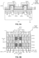
- Figures 2A and 2B illustrate an exemplary FinFET 200 employing first and second dielectric material layers 202(1), 202(2) to apply stress 204 to a channel region 206.
- the FinFET 200 as described herein is designed such that it can be integrated into an integrated circuit (IC) 208.
- Figure 2A illustrates a cross-sectional view of the FinFET 200
- Figure 2B illustrates a top-view of the FinFET 200.
- Components of the FinFET 200 are referred to with common element numbers in Figures 2A and 2B .
- the FinFET 200 includes a substrate 210 and a Fin 212 disposed over the substrate 210.
- the Fin 212 is disposed in a first direction 214.
- the Fin 212 includes a source 216 and a drain 218.
- the channel region 206 of the FinFET 200 is disposed in the Fin 212 between the source 216 and drain 218.
- a gate 220 is disposed around the channel region 206.
- the gate 220 is formed as a high-dielectric metal gate (HKMG).
- a gate oxide layer 222, a gate dielectric material layer 224, a work function layer 226, and a conductive layer 228 are employed to form the gate 220.
- other aspects of the FinFET 200 may employ gate types other than the HKMG described herein.
- the FinFET 200 can also employ gate structures 230(1)-230(4) configured to function as dummy gates.
- the first dielectric material layer 202(1) is disposed over the substrate 210 and adjacent to a first side 232(1) of the Fin 212.
- the second dielectric material layer 202(2) is disposed over the substrate 210 and adjacent to a second side 232(2) of the Fin 212 that is different from the first side 232(1).
- the first and second dielectric material layers 202(1), 202(2) are disposed in the first direction 214.
- top surfaces 234(1), 234(2) of the first and second dielectric material layers 202(1), 202(2), respectively, are lower than a top surface 236 of the Fin 212 so as to leave space to form the gate 220.
- the first and second dielectric material layers 202(1), 202(2) are disposed within an active area boundary 238 that surrounds an active layer 240 of the FinFET 200.
- the active layer 240 of the FinFET 200 corresponds to doped regions of the substrate 210 on which active elements, such as sources and drains of the FinFET 200 may be formed.
- the first and second dielectric material layers 202(1), 202(2) can be limited to the active area boundary 238 so as to apply the stress 204 to the channel region 206 while avoiding disposing material to inactive or non-doped regions where the stress 204 is not applicable.
- the first and second dielectric material layers 202(1), 202(2) in this aspect are formed from one or more oxide materials disposed (e.g., deposited) over the substrate 210 using a process such as flowable chemical vapor deposition (FCVP) or high aspect ratio processing (HARP).
- FCVP flowable chemical vapor deposition
- HTP high aspect ratio processing
- the oxide material(s) of the first and second dielectric material layers 202(1), 202(2) are thermally annealed to apply a particular type or magnitude of the stress 204.
- the first and second dielectric material layers 202(1), 202(2) can be formed from silicon dioxide. Instead of an oxide material, silicon nitride may also be used.
- the FinFET 200 is an N-type FinFET
- the first and second dielectric material layers 202(1), 202(2) are thermally annealed such that the stress 204 applied to the channel region 206 is tensile stress.
- the FinFET 200 is a P-type FinFET
- the first and second dielectric material layers 202(1), 202(2) are thermally annealed such that the stress 204 applied to the channel region 206 is compressive stress.
- disposing and annealing the oxide material(s) of the first and second dielectric material layers 202(1), 202(2) as described above applies the stress 204 along the Fin 212, including the channel region 206.
- the level of the stress 204 applied by the first and second dielectric material layers 202(1), 202(2) is not dependent on the volume of the first and second dielectric material layers 202(1), 202(2).
- the magnitude of the stress applied by the epitaxial layers correlates to the volume of such layers.
- the first and second dielectric material layers 202(1), 202(2) may provide a consistent level of stress 204 on the channel region 206 even as the area of the FinFET 200 decreases.
- the stress 204 using the first and second dielectric material layers 202(1), 202(2) does not increase area of the FinFET 200.
- the STI structures 242(1), 242(2) can be designed to induce stress by increasing a width of each STI structure 242(1), 242(2).
- An increased width of the STI structures 242(1), 242(2) increases the area of the circuit employing the FinFET 200.
- an increased width of the STI structures 242(1), 242(2) reduces the magnitude of stress applied to the FinFET 200.
- the magnitude of the stress applied by the STI structures 242(1), 242(2) is inversely proportional to the width of the STI structures 242(1), 242(2).
- the resulting applied stress is reduced. Therefore, in addition to providing consistent stress 204 even as the area of the FinFET 200 decreases, the first and second dielectric material layers 202(1), 202(2) apply the stress 204 at a consistent magnitude without increasing area.
- Figures 3A and 3B illustrate an exemplary fabrication process 300 employed to fabricate the FinFET 200 in Figures 2A and 2B .
- Figures 4A-4D provide cross-sectional and top view diagrams illustrating respective stages 400(1)-400(4) of the FinFET 200 during the fabrication process 300.
- the cross-sectional and top-view diagrams illustrating the FinFET 200 in Figures 4A-4D will be discussed in conjunction with the discussion of the exemplary fabrication steps in the fabrication process 300 in Figures 3A and 3B .
- the fabrication process 300 beginning in Figure 3A includes providing the substrate 210 including the Fin 212 (block 302, stage 400(1) of Fig. 4A ).
- the Fin 212 is disposed in the first direction 214.
- the fabrication process 300 also includes disposing the first dielectric material layer 202(1) over the substrate 210 and adjacent to the first side 232(1) of the Fin 212 (block 304, stage 400(2) of Fig. 4B ).
- the fabrication process 300 further includes disposing the second dielectric material layer 202(2) over the substrate 210 and adjacent to the second side 232(2) of the Fin 212 (block 306, stage 400(2) of Fig. 4B ).
- the first and second dielectric material layers 202(1), 202(2) are disposed in the first direction 214.
- the first and second dielectric material layers 202(1), 202(2) can be disposed over the substrate 210 in blocks 304 and 306 using processes such as flowable chemical vapor deposition (FCVP) or high aspect ratio processing (HARP). Further, the first and second dielectric material layers 202(1), 202(2) can be disposed to be limited to the active area boundary 238.
- FCVP flowable chemical vapor deposition
- HTP high aspect ratio processing
- thermal annealing is employed to adjust the stress 204 applied by the first and second dielectric material layers 202(1), 202(2). More specifically, the fabrication process 300 includes wet annealing the first dielectric material layer 202(1) and the second dielectric material layer 202(2) to adjust the stress 204 applied to the channel region 206 of the FinFET 200 (block 308, stage 400(2) of Fig. 4B ). For example, a low temperature wet anneal process of approximately 600 degrees Celsius (C) may be employed in block 308.
- C degrees Celsius
- the fabrication process 300 also includes dry annealing the first dielectric material layer 202(1) and the second dielectric material layer 202(2) to adjust the stress 204 applied to the channel region 206 of the FinFET 200 (block 310, stage 400(2) of Fig. 4B ).
- dry annealing process of approximately 1050 C can be employed in block 310.
- the fabrication process 300 can include etching the Fin 212 corresponding to a source region 402 of the FinFET 200 on a first side 404(1) of a gate region 406 (block 312, stage 400(2) of Fig. 4B ).
- the fabrication process 300 can also include etching the Fin 212 corresponding to a drain region 408 of the FinFET 200 on a second side 404(2) of the gate region 406 different from the first side 404(1) (block 314, stage 400(2) of Fig. 4B ).
- the fabrication process 300 can include growing a source material 410 in the source region 402 (block 316, stage 400(2) of Fig. 4B ).
- the fabrication process 300 can also include growing a drain material 412 in the drain region 408 (block 318, stage 400(2) of Fig. 4B ).
- the fabrication process 300 also includes disposing the gate 220 with a width W approximately equal to a gate length of the FinFET 200 in the gate region 406 (block 320, stages 400(3), 400(4) in Figs. 4C , 4D ).
- the gate length is approximately equal to 10 nm.
- the gate 220 is disposed over the Fin 212, the first dielectric material layer 202(1), and the second dielectric material layer 202(2).
- the gate 220 is disposed in a second direction 414 substantially orthogonal to the first direction 214.
- the gate 220 can be disposed in block 320 by disposing the gate oxide layer 222 with a width W approximately equal to the gate length of the FinFET 200 in the gate region 406 over the Fin 212 (block 322, stage 400(3) of Fig. 4C ). Disposing the gate 220 in block 320 can also include disposing the gate dielectric material layer 224 with the width W approximately equal to the gate length of the FinFET 200 in the gate region 406 (block 324, stage 400(4) of Fig. 4D ). The gate dielectric material layer 224 is disposed in block 324 over the gate oxide layer 222, the first dielectric material layer 202(1), and the second dielectric material layer 202(2).
- Disposing the gate 220 in block 320 can also include disposing the work function layer 226 with the width W approximately equal to the gate length of the FinFET 200 in the gate region 406 (block 326, stage 400(4) of Fig. 4D ).
- the work function layer 226 is disposed over the gate dielectric material layer 224.
- disposing the gate 220 in block 320 can include disposing the conductive layer 228 with the width W approximately equal to the gate length of the FinFET 200 in the gate region 406 over the work function layer 226 (block 328, stage 400(4) of Fig. 4D ).
- Manufacturing the FinFET 200 using the fabrication process 300 enables the FinFET 200 to provide a consistent level of stress 204 to the channel region 206 even as the area of the FinFET 200 decreases. Additionally, the fabrication process 300 includes various steps included in conventional FinFET fabrication methods. Integrating additional steps above for inducing a particular type or magnitude of the stress 204 may include one (1) additional mask as compared to conventional methods. Thus, the FinFET 200 can be fabricated to apply the stress 204 as described above while minimizing increased manufacturing costs and complexity.
- FIG. 5A and 5B illustrate an exemplary FinFET 500 employing first, second, and third dielectric material layers 202(1)-202(3) to apply the stress 204 on first and second channel regions 206(1), 206(2).
- Figure 5A illustrates a cross-sectional view of the FinFET 500
- Figure 5B illustrates a top-view of the FinFET 500.
- Components of the FinFET 500 are referred to with common element numbers in Figures 5A and 5B .
- the FinFET 500 includes certain common components with the FinFET 200 in Figures 2A, 2B , as shown by similar element numbers between Figures 2A, 2B , 5A, and 5B , and thus will not be re-described herein.
- the FinFET 500 includes the substrate 210 and first and second Fins 212(1), 212(2) disposed 214 over the substrate 210.
- the first and second Fins 212(1), 212(2) are disposed in the first direction 214.
- the first and second Fins 212(1), 212(2) are separated by a distance D approximately equal to 32 nm.
- the first and second Fins 212(1), 212(2) each include a source 216(1), 216(2) and a drain 218(1), 218(2), respectively.
- First and second channel regions 206(1), 206(2) of the FinFET 500 are disposed in the first and second Fins 212(1), 212(2), respectively, between the respective source 216(1), 216(2) and drain 218(1), 218(2). Additionally, the gate 220 is disposed around the first and second channel regions 206(1), 206(2). Similar to the FinFET 200, gate oxide layers 222(1), 222(2) over the first and second Fins 212(1), 212(2), respectively, the gate dielectric material layer 224, the work function layer 226, and the conductive layer 228 are employed to form the gate 220.
- the FinFET 500 is designed such that the stress 204 is also applied to the channel region 206(2).
- a third dielectric material layer 202(3) is disposed over the substrate 210 and adjacent to a second side 502(2) of the second Fin 212(2).
- the second dielectric material layer 202(2) is disposed over the substrate 210 and adjacent to a first side 502(1) of the second Fin 212(2) that is different from the second side 502(2).
- the second and third dielectric material layers 202(2), 202(3) are disposed in the first direction 214.
- the second dielectric material layer 202(2) also applies the stress 204 to the channel region 206(2).
- the first, second, and third dielectric material layers 202(1)-202(3) are disposed within an active area boundary 504 that surrounds an active layer 506 of the FinFET 500.
- the first, second, and third dielectric material layers 202(1)-202(3) may provide a consistent level of stress 204 on the first and second channel regions 206(1), 206(2) even as the area of the FinFET 500 decreases.
- the distance D between the first and second Fins 212(1), 212(2) decreases below 32 nm.
- the stress 204 remains consistent even as the distance D decreases, unlike stress induced by epitaxial layers.
- the substrate 210 is sometimes referred to herein as "a means for providing a substrate.”
- the Fin 212 is sometimes referred to herein as "a means for providing a Fin over the substrate.”
- the gate 220 is sometimes referred to herein as "a means for providing a gate around the channel region.”
- the first dielectric material layer 202(1) is sometimes referred to herein as "a means for providing a first dielectric material layer disposed over the substrate and adjacent to a first side of the Fin, wherein the first dielectric material layer applies stress to the channel region.”
- the second dielectric material layer 202(2) is sometimes referred to herein as "a means for providing a second dielectric material layer disposed over the substrate and adjacent to a second side of the Fin different from the first side, wherein the second dielectric material layer applies stress to the channel region.”
- the FINFETs employing dielectric material layers to apply stress to channel regions may be provided in or integrated into any processor-based device.
- Examples include a set top box, an entertainment unit, a navigation device, a communications device, a fixed location data unit, a mobile location data unit, a global positioning system (GPS) device, a mobile phone, a cellular phone, a smart phone, a session initiation protocol (SIP) phone, a tablet, a phablet, a server, a computer, a portable computer, a mobile computing device, a wearable computing device (e.g., a smart watch, a health or fitness tracker, eyewear, etc.), a desktop computer, a personal digital assistant (PDA), a monitor, a computer monitor, a television, a tuner, a radio, a satellite radio, a music player, a digital music player, a portable music player, a digital video player, a video player, a digital video disc (DVD)
- GPS global positioning system
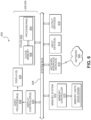
- Figure 6 illustrates an example of a processor-based system 600 that can employ the FinFET 200 illustrated in Figures 2A and 2B , and the FinFET 500 illustrated in Figures 5A and 5B .
- the processor-based system 600 includes one or more central processing units (CPUs) 602, each including one or more processors 604.
- the CPU(s) 602 may have cache memory 606 coupled to the processor(s) 604 for rapid access to temporarily stored data.
- the CPU(s) 602 is coupled to a system bus 608 and can intercouple master and slave devices included in the processor-based system 600.
- the CPU(s) 602 communicates with these other devices by exchanging address, control, and data information over the system bus 608.
- the CPU(s) 602 can communicate bus transaction requests to a memory controller 610 as an example of a slave device.
- multiple system buses 608 could be provided, wherein each system bus 608 constitutes a different fabric.
- Other master and slave devices can be connected to the system bus 608. As illustrated in Figure 6 , these devices can include a memory system 612, one or more input devices 614, one or more output devices 616, one or more network interface devices 618, and one or more display controllers 620, as examples.
- the input device(s) 614 can include any type of input device, including, but not limited to, input keys, switches, voice processors, etc.
- the output device(s) 616 can include any type of output device, including, but not limited to, audio, video, other visual indicators, etc.
- the network interface device(s) 618 can be any device configured to allow exchange of data to and from a network 622.
- the network 622 can be any type of network, including, but not limited to, a wired or wireless network, a private or public network, a local area network (LAN), a wireless local area network (WLAN), a wide area network (WAN), a BLUETOOTH TM network, and the Internet.
- the network interface device(s) 618 can be configured to support any type of communications protocol desired.
- the memory system 612 can include one or more memory units 624(0)-624(M).
- the CPU(s) 602 may also be configured to access the display controller(s) 620 over the system bus 608 to control information sent to one or more displays 626.
- the display controller(s) 620 sends information to the display(s) 626 to be displayed via one or more video processors 628, which process the information to be displayed into a format suitable for the display(s) 626.
- the display(s) 626 can include any type of display, including, but not limited to, a cathode ray tube (CRT), a liquid crystal display (LCD), a plasma display, a light emitting diode (LED) display, etc.
- DSP Digital Signal Processor
- ASIC Application Specific Integrated Circuit
- FPGA Field Programmable Gate Array
- a processor may be a microprocessor, but in the alternative, the processor may be any conventional processor, controller, microcontroller, or state machine.
- a processor may also be implemented as a combination of computing devices (e.g., a combination of a DSP and a microprocessor, a plurality of microprocessors, one or more microprocessors in conjunction with a DSP core, or any other such configuration).
- RAM Random Access Memory
- ROM Read Only Memory
- EPROM Electrically Programmable ROM
- EEPROM Electrically Erasable Programmable ROM
- registers a hard disk, a removable disk, a CD-ROM, or any other form of computer readable medium known in the art.
- An exemplary storage medium is coupled to the processor such that the processor can read information from, and write information to, the storage medium.
- the storage medium may be integral to the processor.
- the processor and the storage medium may reside in an ASIC.
- the ASIC may reside in a remote station.
- the processor and the storage medium may reside as discrete components in a remote station, base station, or server.
Landscapes
- Engineering & Computer Science (AREA)
- Manufacturing & Machinery (AREA)
- General Physics & Mathematics (AREA)
- Chemical Kinetics & Catalysis (AREA)
- Physics & Mathematics (AREA)
- Condensed Matter Physics & Semiconductors (AREA)
- Chemical & Material Sciences (AREA)
- Computer Hardware Design (AREA)
- Microelectronics & Electronic Packaging (AREA)
- Power Engineering (AREA)
- General Chemical & Material Sciences (AREA)
- Thin Film Transistor (AREA)
- Insulated Gate Type Field-Effect Transistor (AREA)
- General Engineering & Computer Science (AREA)
Applications Claiming Priority (2)
| Application Number | Priority Date | Filing Date | Title |
|---|---|---|---|
| US15/266,840 US9882051B1 (en) | 2016-09-15 | 2016-09-15 | Fin field effect transistors (FETs) (FinFETs) employing dielectric material layers to apply stress to channel regions |
| PCT/US2017/046525 WO2018052591A1 (en) | 2016-09-15 | 2017-08-11 | Fin field effect transistors (fets) (finfets) employing dielectric material layers to apply stress to channel regions |
Publications (3)
| Publication Number | Publication Date |
|---|---|
| EP3513437A1 EP3513437A1 (en) | 2019-07-24 |
| EP3513437B1 true EP3513437B1 (en) | 2024-10-30 |
| EP3513437C0 EP3513437C0 (en) | 2024-10-30 |
Family
ID=59684098
Family Applications (1)
| Application Number | Title | Priority Date | Filing Date |
|---|---|---|---|
| EP17755390.6A Active EP3513437B1 (en) | 2016-09-15 | 2017-08-11 | Fin field effect transistors (fets) (finfets) employing dielectric material layers to apply stress to channel regions |
Country Status (8)
Families Citing this family (3)
| Publication number | Priority date | Publication date | Assignee | Title |
|---|---|---|---|---|
| US10109507B2 (en) * | 2016-06-01 | 2018-10-23 | Taiwan Semiconductor Manufacturing Co., Ltd. | Fluorine contamination control in semiconductor manufacturing process |
| US11211243B2 (en) | 2018-11-21 | 2021-12-28 | Taiwan Semiconductor Manufacturing Company, Ltd. | Method of filling gaps with carbon and nitrogen doped film |
| KR102760190B1 (ko) * | 2019-05-16 | 2025-01-23 | 삼성전자주식회사 | 반도체 장치 및 그 제조 방법 |
Family Cites Families (20)
| Publication number | Priority date | Publication date | Assignee | Title |
|---|---|---|---|---|
| US7081395B2 (en) | 2003-05-23 | 2006-07-25 | Taiwan Semiconductor Manufacturing Co., Ltd. | Silicon strain engineering accomplished via use of specific shallow trench isolation fill materials |
| JP2007207837A (ja) | 2006-01-31 | 2007-08-16 | Toshiba Corp | 半導体装置および半導体装置の製造方法 |
| US7939862B2 (en) | 2007-05-30 | 2011-05-10 | Synopsys, Inc. | Stress-enhanced performance of a FinFet using surface/channel orientations and strained capping layers |
| US7943531B2 (en) * | 2007-10-22 | 2011-05-17 | Applied Materials, Inc. | Methods for forming a silicon oxide layer over a substrate |
| US7915112B2 (en) | 2008-09-23 | 2011-03-29 | Taiwan Semiconductor Manufacturing Company, Ltd. | Metal gate stress film for mobility enhancement in FinFET device |
| US9953885B2 (en) * | 2009-10-27 | 2018-04-24 | Taiwan Semiconductor Manufacturing Company, Ltd. | STI shape near fin bottom of Si fin in bulk FinFET |
| US8426923B2 (en) * | 2009-12-02 | 2013-04-23 | Taiwan Semiconductor Manufacturing Company, Ltd. | Multiple-gate semiconductor device and method |
| DE102010002410B4 (de) | 2010-02-26 | 2017-03-02 | Globalfoundries Dresden Module One Limited Liability Company & Co. Kg | Verformungsgedächtnistechnologie in verformten SOI-Substraten von Halbleiterbauelementen |
| US8937353B2 (en) * | 2010-03-01 | 2015-01-20 | Taiwan Semiconductor Manufacturing Co., Ltd. | Dual epitaxial process for a finFET device |
| JP2013093438A (ja) * | 2011-10-26 | 2013-05-16 | Renesas Electronics Corp | 半導体装置の製造方法 |
| US8698199B2 (en) | 2012-01-11 | 2014-04-15 | United Microelectronics Corp. | FinFET structure |
| US8941187B2 (en) | 2012-01-13 | 2015-01-27 | Globalfoundries Inc. | Strain engineering in three-dimensional transistors based on strained isolation material |
| CN103681846B (zh) | 2012-09-20 | 2017-02-08 | 中芯国际集成电路制造(上海)有限公司 | 半导体装置及其制造方法 |
| US9263585B2 (en) * | 2012-10-30 | 2016-02-16 | Globalfoundries Inc. | Methods of forming enhanced mobility channel regions on 3D semiconductor devices, and devices comprising same |
| US8759874B1 (en) * | 2012-11-30 | 2014-06-24 | Stmicroelectronics, Inc. | FinFET device with isolated channel |
| US8877588B2 (en) | 2013-02-11 | 2014-11-04 | Globalfoundries Inc. | Methods of forming a three-dimensional semiconductor device with a dual stress channel and the resulting device |
| US9721955B2 (en) | 2014-04-25 | 2017-08-01 | Taiwan Semiconductor Manufacturing Company, Ltd. | Structure and method for SRAM FinFET device having an oxide feature |
| US9306067B2 (en) | 2014-08-05 | 2016-04-05 | Taiwan Semiconductor Manufacturing Company, Ltd. | Nonplanar device and strain-generating channel dielectric |
| TWI655774B (zh) * | 2015-08-12 | 2019-04-01 | 聯華電子股份有限公司 | 半導體元件及其製作方法 |
| US9614086B1 (en) * | 2015-12-30 | 2017-04-04 | Taiwan Semiconductor Manufacturing Company, Ltd. | Conformal source and drain contacts for multi-gate field effect transistors |
-
2016
- 2016-09-15 US US15/266,840 patent/US9882051B1/en active Active
-
2017
- 2017-08-11 KR KR1020197007266A patent/KR102550579B1/ko active Active
- 2017-08-11 CN CN201780056420.3A patent/CN109844957A/zh active Pending
- 2017-08-11 CA CA3032965A patent/CA3032965A1/en active Pending
- 2017-08-11 JP JP2019513978A patent/JP6974446B2/ja active Active
- 2017-08-11 WO PCT/US2017/046525 patent/WO2018052591A1/en active Search and Examination
- 2017-08-11 EP EP17755390.6A patent/EP3513437B1/en active Active
- 2017-08-11 BR BR112019004507-4A patent/BR112019004507B1/pt active IP Right Grant
Also Published As
| Publication number | Publication date |
|---|---|
| KR20190047696A (ko) | 2019-05-08 |
| BR112019004507B1 (pt) | 2023-10-03 |
| EP3513437C0 (en) | 2024-10-30 |
| KR102550579B1 (ko) | 2023-07-03 |
| JP6974446B2 (ja) | 2021-12-01 |
| WO2018052591A1 (en) | 2018-03-22 |
| CA3032965A1 (en) | 2018-03-22 |
| JP2019530227A (ja) | 2019-10-17 |
| US9882051B1 (en) | 2018-01-30 |
| BR112019004507A2 (pt) | 2019-06-04 |
| EP3513437A1 (en) | 2019-07-24 |
| CN109844957A (zh) | 2019-06-04 |
Similar Documents
| Publication | Publication Date | Title |
|---|---|---|
| US9570442B1 (en) | Applying channel stress to Fin field-effect transistors (FETs) (FinFETs) using a self-aligned single diffusion break (SDB) isolation structure | |
| US10134734B2 (en) | Fin field effect transistor (FET) (FinFET) complementary metal oxide semiconductor (CMOS) circuits employing single and double diffusion breaks for increased performance | |
| CN104011841B (zh) | 用于形成金属氧化物半导体器件结构的鳍的方法 | |
| US10847656B2 (en) | Fabrication of non-planar IGZO devices for improved electrostatics | |
| US10115723B2 (en) | Complementary metal oxide semiconductor (CMOS) devices employing plasma-doped source/drain structures and related methods | |
| US10109646B1 (en) | Selectively recessing trench isolation in three-dimensional (3D) transistors to vary channel structure exposures from trench isolation to control drive strength | |
| US10361090B2 (en) | Vertical channel transistors fabrication process by selective subtraction of a regular grid | |
| US20180212029A1 (en) | Semiconductor devices employing reduced area conformal contacts to reduce parasitic capacitance, and related methods | |
| EP3513437B1 (en) | Fin field effect transistors (fets) (finfets) employing dielectric material layers to apply stress to channel regions | |
| US20200273998A1 (en) | Source electrode and drain electrode protection for nanowire transistors | |
| EP3378095B1 (en) | Semiconductor devices with wider field gates for reduced gate resistance | |
| US11798838B2 (en) | Capacitance reduction for semiconductor devices based on wafer bonding | |
| US10714582B2 (en) | Controlling dimensions of a negative capacitance layer of a gate stack of a field-effect transistor (FET) to increase power density | |
| EP3513429B1 (en) | Semiconductor devices employing field effect transistors (fets) with multiple channel structures without shallow trench isolation (sti) void-induced electrical shorts | |
| US20190296126A1 (en) | Systems and methods for dummy gate tie-offs in a self-aligned gate contact (sagc) cell | |
| US10600774B2 (en) | Systems and methods for fabrication of gated diodes with selective epitaxial growth | |
| HK40008500A (en) | Semiconductor devices employing field effect transistors (fets) with multiple channel structures without shallow trench isolation (sti) void-induced electrical shorts | |
| US20160293477A1 (en) | Silicon-on-insulator (soi) wafers employing molded substrates to improve insulation and reduce current leakage |
Legal Events
| Date | Code | Title | Description |
|---|---|---|---|
| STAA | Information on the status of an ep patent application or granted ep patent |
Free format text: STATUS: UNKNOWN |
|
| STAA | Information on the status of an ep patent application or granted ep patent |
Free format text: STATUS: THE INTERNATIONAL PUBLICATION HAS BEEN MADE |
|
| PUAI | Public reference made under article 153(3) epc to a published international application that has entered the european phase |
Free format text: ORIGINAL CODE: 0009012 |
|
| STAA | Information on the status of an ep patent application or granted ep patent |
Free format text: STATUS: REQUEST FOR EXAMINATION WAS MADE |
|
| 17P | Request for examination filed |
Effective date: 20190204 |
|
| AK | Designated contracting states |
Kind code of ref document: A1 Designated state(s): AL AT BE BG CH CY CZ DE DK EE ES FI FR GB GR HR HU IE IS IT LI LT LU LV MC MK MT NL NO PL PT RO RS SE SI SK SM TR |
|
| AX | Request for extension of the european patent |
Extension state: BA ME |
|
| DAV | Request for validation of the european patent (deleted) | ||
| DAX | Request for extension of the european patent (deleted) | ||
| STAA | Information on the status of an ep patent application or granted ep patent |
Free format text: STATUS: EXAMINATION IS IN PROGRESS |
|
| STAA | Information on the status of an ep patent application or granted ep patent |
Free format text: STATUS: EXAMINATION IS IN PROGRESS |
|
| 17Q | First examination report despatched |
Effective date: 20211008 |
|
| GRAP | Despatch of communication of intention to grant a patent |
Free format text: ORIGINAL CODE: EPIDOSNIGR1 |
|
| STAA | Information on the status of an ep patent application or granted ep patent |
Free format text: STATUS: GRANT OF PATENT IS INTENDED |
|
| INTG | Intention to grant announced |
Effective date: 20240529 |
|
| GRAS | Grant fee paid |
Free format text: ORIGINAL CODE: EPIDOSNIGR3 |
|
| GRAA | (expected) grant |
Free format text: ORIGINAL CODE: 0009210 |
|
| STAA | Information on the status of an ep patent application or granted ep patent |
Free format text: STATUS: THE PATENT HAS BEEN GRANTED |
|
| AK | Designated contracting states |
Kind code of ref document: B1 Designated state(s): AL AT BE BG CH CY CZ DE DK EE ES FI FR GB GR HR HU IE IS IT LI LT LU LV MC MK MT NL NO PL PT RO RS SE SI SK SM TR |
|
| REG | Reference to a national code |
Ref country code: GB Ref legal event code: FG4D |
|
| REG | Reference to a national code |
Ref country code: CH Ref legal event code: EP |
|
| REG | Reference to a national code |
Ref country code: IE Ref legal event code: FG4D |
|
| REG | Reference to a national code |
Ref country code: DE Ref legal event code: R096 Ref document number: 602017085778 Country of ref document: DE |
|
| REG | Reference to a national code |
Ref country code: DE Ref legal event code: R079 Ref document number: 602017085778 Country of ref document: DE Free format text: PREVIOUS MAIN CLASS: H01L0029780000 Ipc: H10D0030600000 |
|
| U01 | Request for unitary effect filed |
Effective date: 20241112 |
|
| U07 | Unitary effect registered |
Designated state(s): AT BE BG DE DK EE FI FR IT LT LU LV MT NL PT RO SE SI Effective date: 20241120 |
|
| PG25 | Lapsed in a contracting state [announced via postgrant information from national office to epo] |
Ref country code: HR Free format text: LAPSE BECAUSE OF FAILURE TO SUBMIT A TRANSLATION OF THE DESCRIPTION OR TO PAY THE FEE WITHIN THE PRESCRIBED TIME-LIMIT Effective date: 20241030 Ref country code: IS Free format text: LAPSE BECAUSE OF FAILURE TO SUBMIT A TRANSLATION OF THE DESCRIPTION OR TO PAY THE FEE WITHIN THE PRESCRIBED TIME-LIMIT Effective date: 20250228 |
|
| PG25 | Lapsed in a contracting state [announced via postgrant information from national office to epo] |
Ref country code: ES Free format text: LAPSE BECAUSE OF FAILURE TO SUBMIT A TRANSLATION OF THE DESCRIPTION OR TO PAY THE FEE WITHIN THE PRESCRIBED TIME-LIMIT Effective date: 20241030 |
|
| PG25 | Lapsed in a contracting state [announced via postgrant information from national office to epo] |
Ref country code: NO Free format text: LAPSE BECAUSE OF FAILURE TO SUBMIT A TRANSLATION OF THE DESCRIPTION OR TO PAY THE FEE WITHIN THE PRESCRIBED TIME-LIMIT Effective date: 20250130 |
|
| PG25 | Lapsed in a contracting state [announced via postgrant information from national office to epo] |
Ref country code: GR Free format text: LAPSE BECAUSE OF FAILURE TO SUBMIT A TRANSLATION OF THE DESCRIPTION OR TO PAY THE FEE WITHIN THE PRESCRIBED TIME-LIMIT Effective date: 20250131 |
|
| PG25 | Lapsed in a contracting state [announced via postgrant information from national office to epo] |
Ref country code: PL Free format text: LAPSE BECAUSE OF FAILURE TO SUBMIT A TRANSLATION OF THE DESCRIPTION OR TO PAY THE FEE WITHIN THE PRESCRIBED TIME-LIMIT Effective date: 20241030 |
|
| PG25 | Lapsed in a contracting state [announced via postgrant information from national office to epo] |
Ref country code: RS Free format text: LAPSE BECAUSE OF FAILURE TO SUBMIT A TRANSLATION OF THE DESCRIPTION OR TO PAY THE FEE WITHIN THE PRESCRIBED TIME-LIMIT Effective date: 20250130 |
|
| PG25 | Lapsed in a contracting state [announced via postgrant information from national office to epo] |
Ref country code: SM Free format text: LAPSE BECAUSE OF FAILURE TO SUBMIT A TRANSLATION OF THE DESCRIPTION OR TO PAY THE FEE WITHIN THE PRESCRIBED TIME-LIMIT Effective date: 20241030 |
|
| PG25 | Lapsed in a contracting state [announced via postgrant information from national office to epo] |
Ref country code: SK Free format text: LAPSE BECAUSE OF FAILURE TO SUBMIT A TRANSLATION OF THE DESCRIPTION OR TO PAY THE FEE WITHIN THE PRESCRIBED TIME-LIMIT Effective date: 20241030 |
|
| PG25 | Lapsed in a contracting state [announced via postgrant information from national office to epo] |
Ref country code: CZ Free format text: LAPSE BECAUSE OF FAILURE TO SUBMIT A TRANSLATION OF THE DESCRIPTION OR TO PAY THE FEE WITHIN THE PRESCRIBED TIME-LIMIT Effective date: 20241030 |
|
| U20 | Renewal fee for the european patent with unitary effect paid |
Year of fee payment: 9 Effective date: 20250710 |