EP3509118A1 - Solar cell and method of manufacturing solar cell - Google Patents
Solar cell and method of manufacturing solar cell Download PDFInfo
- Publication number
- EP3509118A1 EP3509118A1 EP17846648.8A EP17846648A EP3509118A1 EP 3509118 A1 EP3509118 A1 EP 3509118A1 EP 17846648 A EP17846648 A EP 17846648A EP 3509118 A1 EP3509118 A1 EP 3509118A1
- Authority
- EP
- European Patent Office
- Prior art keywords
- electrode layer
- solar cell
- cell element
- arrayed
- semiconductor
- Prior art date
- Legal status (The legal status is an assumption and is not a legal conclusion. Google has not performed a legal analysis and makes no representation as to the accuracy of the status listed.)
- Pending
Links
- 238000004519 manufacturing process Methods 0.000 title claims description 15
- 239000004065 semiconductor Substances 0.000 claims abstract description 132
- 238000002834 transmittance Methods 0.000 claims abstract description 35
- 239000000758 substrate Substances 0.000 claims description 46
- 239000002184 metal Substances 0.000 claims description 9
- 229910052751 metal Inorganic materials 0.000 claims description 9
- 238000000034 method Methods 0.000 claims description 9
- 238000006243 chemical reaction Methods 0.000 description 17
- 239000000463 material Substances 0.000 description 12
- 238000010438 heat treatment Methods 0.000 description 7
- 239000002994 raw material Substances 0.000 description 7
- XLOMVQKBTHCTTD-UHFFFAOYSA-N Zinc monoxide Chemical compound [Zn]=O XLOMVQKBTHCTTD-UHFFFAOYSA-N 0.000 description 6
- 239000007788 liquid Substances 0.000 description 6
- 238000010248 power generation Methods 0.000 description 6
- 238000001035 drying Methods 0.000 description 5
- 230000005525 hole transport Effects 0.000 description 5
- 238000000926 separation method Methods 0.000 description 5
- 239000010409 thin film Substances 0.000 description 5
- -1 CH3NH3 + Chemical class 0.000 description 4
- 239000013078 crystal Substances 0.000 description 4
- 150000001768 cations Chemical class 0.000 description 3
- 238000000576 coating method Methods 0.000 description 3
- 239000011521 glass Substances 0.000 description 3
- 238000007740 vapor deposition Methods 0.000 description 3
- 239000011248 coating agent Substances 0.000 description 2
- 150000001875 compounds Chemical class 0.000 description 2
- 239000004020 conductor Substances 0.000 description 2
- 239000005038 ethylene vinyl acetate Substances 0.000 description 2
- 150000004820 halides Chemical class 0.000 description 2
- AMGQUBHHOARCQH-UHFFFAOYSA-N indium;oxotin Chemical compound [In].[Sn]=O AMGQUBHHOARCQH-UHFFFAOYSA-N 0.000 description 2
- 238000000059 patterning Methods 0.000 description 2
- 229920001200 poly(ethylene-vinyl acetate) Polymers 0.000 description 2
- XOLBLPGZBRYERU-UHFFFAOYSA-N tin dioxide Chemical compound O=[Sn]=O XOLBLPGZBRYERU-UHFFFAOYSA-N 0.000 description 2
- 229910001887 tin oxide Inorganic materials 0.000 description 2
- 239000011787 zinc oxide Substances 0.000 description 2
- XDXWNHPWWKGTKO-UHFFFAOYSA-N 207739-72-8 Chemical compound C1=CC(OC)=CC=C1N(C=1C=C2C3(C4=CC(=CC=C4C2=CC=1)N(C=1C=CC(OC)=CC=1)C=1C=CC(OC)=CC=1)C1=CC(=CC=C1C1=CC=C(C=C13)N(C=1C=CC(OC)=CC=1)C=1C=CC(OC)=CC=1)N(C=1C=CC(OC)=CC=1)C=1C=CC(OC)=CC=1)C1=CC=C(OC)C=C1 XDXWNHPWWKGTKO-UHFFFAOYSA-N 0.000 description 1
- 241000887125 Chaptalia nutans Species 0.000 description 1
- XUIMIQQOPSSXEZ-UHFFFAOYSA-N Silicon Chemical compound [Si] XUIMIQQOPSSXEZ-UHFFFAOYSA-N 0.000 description 1
- NIXOWILDQLNWCW-UHFFFAOYSA-N acrylic acid group Chemical group C(C=C)(=O)O NIXOWILDQLNWCW-UHFFFAOYSA-N 0.000 description 1
- 150000003973 alkyl amines Chemical class 0.000 description 1
- 229910052782 aluminium Inorganic materials 0.000 description 1
- XAGFODPZIPBFFR-UHFFFAOYSA-N aluminium Chemical compound [Al] XAGFODPZIPBFFR-UHFFFAOYSA-N 0.000 description 1
- 150000001450 anions Chemical class 0.000 description 1
- 238000000354 decomposition reaction Methods 0.000 description 1
- 150000004985 diamines Chemical class 0.000 description 1
- 239000005357 flat glass Substances 0.000 description 1
- 230000004907 flux Effects 0.000 description 1
- 230000001678 irradiating effect Effects 0.000 description 1
- 239000007769 metal material Substances 0.000 description 1
- 238000012986 modification Methods 0.000 description 1
- 230000004048 modification Effects 0.000 description 1
- 229920000515 polycarbonate Polymers 0.000 description 1
- 239000004417 polycarbonate Substances 0.000 description 1
- 239000003566 sealing material Substances 0.000 description 1
- 229910052710 silicon Inorganic materials 0.000 description 1
- 239000010703 silicon Substances 0.000 description 1
- 239000002904 solvent Substances 0.000 description 1
- 238000004544 sputter deposition Methods 0.000 description 1
- 239000005341 toughened glass Substances 0.000 description 1
Images




Classifications
-
- H—ELECTRICITY
- H10—SEMICONDUCTOR DEVICES; ELECTRIC SOLID-STATE DEVICES NOT OTHERWISE PROVIDED FOR
- H10K—ORGANIC ELECTRIC SOLID-STATE DEVICES
- H10K30/00—Organic devices sensitive to infrared radiation, light, electromagnetic radiation of shorter wavelength or corpuscular radiation
- H10K30/50—Photovoltaic [PV] devices
- H10K30/57—Photovoltaic [PV] devices comprising multiple junctions, e.g. tandem PV cells
-
- H—ELECTRICITY
- H10—SEMICONDUCTOR DEVICES; ELECTRIC SOLID-STATE DEVICES NOT OTHERWISE PROVIDED FOR
- H10F—INORGANIC SEMICONDUCTOR DEVICES SENSITIVE TO INFRARED RADIATION, LIGHT, ELECTROMAGNETIC RADIATION OF SHORTER WAVELENGTH OR CORPUSCULAR RADIATION
- H10F19/00—Integrated devices, or assemblies of multiple devices, comprising at least one photovoltaic cell covered by group H10F10/00, e.g. photovoltaic modules
- H10F19/30—Integrated devices, or assemblies of multiple devices, comprising at least one photovoltaic cell covered by group H10F10/00, e.g. photovoltaic modules comprising thin-film photovoltaic cells
- H10F19/31—Integrated devices, or assemblies of multiple devices, comprising at least one photovoltaic cell covered by group H10F10/00, e.g. photovoltaic modules comprising thin-film photovoltaic cells having multiple laterally adjacent thin-film photovoltaic cells deposited on the same substrate
-
- H—ELECTRICITY
- H10—SEMICONDUCTOR DEVICES; ELECTRIC SOLID-STATE DEVICES NOT OTHERWISE PROVIDED FOR
- H10F—INORGANIC SEMICONDUCTOR DEVICES SENSITIVE TO INFRARED RADIATION, LIGHT, ELECTROMAGNETIC RADIATION OF SHORTER WAVELENGTH OR CORPUSCULAR RADIATION
- H10F19/00—Integrated devices, or assemblies of multiple devices, comprising at least one photovoltaic cell covered by group H10F10/00, e.g. photovoltaic modules
- H10F19/30—Integrated devices, or assemblies of multiple devices, comprising at least one photovoltaic cell covered by group H10F10/00, e.g. photovoltaic modules comprising thin-film photovoltaic cells
- H10F19/31—Integrated devices, or assemblies of multiple devices, comprising at least one photovoltaic cell covered by group H10F10/00, e.g. photovoltaic modules comprising thin-film photovoltaic cells having multiple laterally adjacent thin-film photovoltaic cells deposited on the same substrate
- H10F19/33—Patterning processes to connect the photovoltaic cells, e.g. laser cutting of conductive or active layers
-
- H—ELECTRICITY
- H10—SEMICONDUCTOR DEVICES; ELECTRIC SOLID-STATE DEVICES NOT OTHERWISE PROVIDED FOR
- H10F—INORGANIC SEMICONDUCTOR DEVICES SENSITIVE TO INFRARED RADIATION, LIGHT, ELECTROMAGNETIC RADIATION OF SHORTER WAVELENGTH OR CORPUSCULAR RADIATION
- H10F19/00—Integrated devices, or assemblies of multiple devices, comprising at least one photovoltaic cell covered by group H10F10/00, e.g. photovoltaic modules
- H10F19/30—Integrated devices, or assemblies of multiple devices, comprising at least one photovoltaic cell covered by group H10F10/00, e.g. photovoltaic modules comprising thin-film photovoltaic cells
- H10F19/31—Integrated devices, or assemblies of multiple devices, comprising at least one photovoltaic cell covered by group H10F10/00, e.g. photovoltaic modules comprising thin-film photovoltaic cells having multiple laterally adjacent thin-film photovoltaic cells deposited on the same substrate
- H10F19/35—Structures for the connecting of adjacent photovoltaic cells, e.g. interconnections or insulating spacers
-
- H—ELECTRICITY
- H10—SEMICONDUCTOR DEVICES; ELECTRIC SOLID-STATE DEVICES NOT OTHERWISE PROVIDED FOR
- H10F—INORGANIC SEMICONDUCTOR DEVICES SENSITIVE TO INFRARED RADIATION, LIGHT, ELECTROMAGNETIC RADIATION OF SHORTER WAVELENGTH OR CORPUSCULAR RADIATION
- H10F77/00—Constructional details of devices covered by this subclass
- H10F77/40—Optical elements or arrangements
- H10F77/42—Optical elements or arrangements directly associated or integrated with photovoltaic cells, e.g. light-reflecting means or light-concentrating means
-
- H—ELECTRICITY
- H10—SEMICONDUCTOR DEVICES; ELECTRIC SOLID-STATE DEVICES NOT OTHERWISE PROVIDED FOR
- H10K—ORGANIC ELECTRIC SOLID-STATE DEVICES
- H10K30/00—Organic devices sensitive to infrared radiation, light, electromagnetic radiation of shorter wavelength or corpuscular radiation
- H10K30/80—Constructional details
-
- H—ELECTRICITY
- H10—SEMICONDUCTOR DEVICES; ELECTRIC SOLID-STATE DEVICES NOT OTHERWISE PROVIDED FOR
- H10K—ORGANIC ELECTRIC SOLID-STATE DEVICES
- H10K30/00—Organic devices sensitive to infrared radiation, light, electromagnetic radiation of shorter wavelength or corpuscular radiation
- H10K30/80—Constructional details
- H10K30/87—Light-trapping means
-
- H—ELECTRICITY
- H10—SEMICONDUCTOR DEVICES; ELECTRIC SOLID-STATE DEVICES NOT OTHERWISE PROVIDED FOR
- H10K—ORGANIC ELECTRIC SOLID-STATE DEVICES
- H10K39/00—Integrated devices, or assemblies of multiple devices, comprising at least one organic radiation-sensitive element covered by group H10K30/00
- H10K39/10—Organic photovoltaic [PV] modules; Arrays of single organic PV cells
-
- H—ELECTRICITY
- H10—SEMICONDUCTOR DEVICES; ELECTRIC SOLID-STATE DEVICES NOT OTHERWISE PROVIDED FOR
- H10K—ORGANIC ELECTRIC SOLID-STATE DEVICES
- H10K39/00—Integrated devices, or assemblies of multiple devices, comprising at least one organic radiation-sensitive element covered by group H10K30/00
- H10K39/10—Organic photovoltaic [PV] modules; Arrays of single organic PV cells
- H10K39/12—Electrical configurations of PV cells, e.g. series connections or parallel connections
-
- H—ELECTRICITY
- H10—SEMICONDUCTOR DEVICES; ELECTRIC SOLID-STATE DEVICES NOT OTHERWISE PROVIDED FOR
- H10K—ORGANIC ELECTRIC SOLID-STATE DEVICES
- H10K71/00—Manufacture or treatment specially adapted for the organic devices covered by this subclass
- H10K71/20—Changing the shape of the active layer in the devices, e.g. patterning
- H10K71/211—Changing the shape of the active layer in the devices, e.g. patterning by selective transformation of an existing layer
-
- H—ELECTRICITY
- H10—SEMICONDUCTOR DEVICES; ELECTRIC SOLID-STATE DEVICES NOT OTHERWISE PROVIDED FOR
- H10K—ORGANIC ELECTRIC SOLID-STATE DEVICES
- H10K71/00—Manufacture or treatment specially adapted for the organic devices covered by this subclass
- H10K71/40—Thermal treatment, e.g. annealing in the presence of a solvent vapour
- H10K71/421—Thermal treatment, e.g. annealing in the presence of a solvent vapour using coherent electromagnetic radiation, e.g. laser annealing
-
- H—ELECTRICITY
- H10—SEMICONDUCTOR DEVICES; ELECTRIC SOLID-STATE DEVICES NOT OTHERWISE PROVIDED FOR
- H10K—ORGANIC ELECTRIC SOLID-STATE DEVICES
- H10K85/00—Organic materials used in the body or electrodes of devices covered by this subclass
- H10K85/50—Organic perovskites; Hybrid organic-inorganic perovskites [HOIP], e.g. CH3NH3PbI3
-
- H—ELECTRICITY
- H01—ELECTRIC ELEMENTS
- H01G—CAPACITORS; CAPACITORS, RECTIFIERS, DETECTORS, SWITCHING DEVICES, LIGHT-SENSITIVE OR TEMPERATURE-SENSITIVE DEVICES OF THE ELECTROLYTIC TYPE
- H01G9/00—Electrolytic capacitors, rectifiers, detectors, switching devices, light-sensitive or temperature-sensitive devices; Processes of their manufacture
- H01G9/20—Light-sensitive devices
- H01G9/2068—Panels or arrays of photoelectrochemical cells, e.g. photovoltaic modules based on photoelectrochemical cells
- H01G9/2081—Serial interconnection of cells
-
- H—ELECTRICITY
- H01—ELECTRIC ELEMENTS
- H01G—CAPACITORS; CAPACITORS, RECTIFIERS, DETECTORS, SWITCHING DEVICES, LIGHT-SENSITIVE OR TEMPERATURE-SENSITIVE DEVICES OF THE ELECTROLYTIC TYPE
- H01G9/00—Electrolytic capacitors, rectifiers, detectors, switching devices, light-sensitive or temperature-sensitive devices; Processes of their manufacture
- H01G9/20—Light-sensitive devices
- H01G9/209—Light trapping arrangements
-
- H—ELECTRICITY
- H10—SEMICONDUCTOR DEVICES; ELECTRIC SOLID-STATE DEVICES NOT OTHERWISE PROVIDED FOR
- H10F—INORGANIC SEMICONDUCTOR DEVICES SENSITIVE TO INFRARED RADIATION, LIGHT, ELECTROMAGNETIC RADIATION OF SHORTER WAVELENGTH OR CORPUSCULAR RADIATION
- H10F19/00—Integrated devices, or assemblies of multiple devices, comprising at least one photovoltaic cell covered by group H10F10/00, e.g. photovoltaic modules
- H10F19/30—Integrated devices, or assemblies of multiple devices, comprising at least one photovoltaic cell covered by group H10F10/00, e.g. photovoltaic modules comprising thin-film photovoltaic cells
- H10F19/31—Integrated devices, or assemblies of multiple devices, comprising at least one photovoltaic cell covered by group H10F10/00, e.g. photovoltaic modules comprising thin-film photovoltaic cells having multiple laterally adjacent thin-film photovoltaic cells deposited on the same substrate
- H10F19/37—Integrated devices, or assemblies of multiple devices, comprising at least one photovoltaic cell covered by group H10F10/00, e.g. photovoltaic modules comprising thin-film photovoltaic cells having multiple laterally adjacent thin-film photovoltaic cells deposited on the same substrate comprising means for obtaining partial light transmission through the integrated devices, or the assemblies of multiple devices, e.g. partially transparent thin-film photovoltaic modules for windows
-
- H—ELECTRICITY
- H10—SEMICONDUCTOR DEVICES; ELECTRIC SOLID-STATE DEVICES NOT OTHERWISE PROVIDED FOR
- H10K—ORGANIC ELECTRIC SOLID-STATE DEVICES
- H10K19/00—Integrated devices, or assemblies of multiple devices, comprising at least one organic element specially adapted for rectifying, amplifying, oscillating or switching, covered by group H10K10/00
- H10K19/20—Integrated devices, or assemblies of multiple devices, comprising at least one organic element specially adapted for rectifying, amplifying, oscillating or switching, covered by group H10K10/00 comprising components having an active region that includes an inorganic semiconductor
-
- H—ELECTRICITY
- H10—SEMICONDUCTOR DEVICES; ELECTRIC SOLID-STATE DEVICES NOT OTHERWISE PROVIDED FOR
- H10K—ORGANIC ELECTRIC SOLID-STATE DEVICES
- H10K2102/00—Constructional details relating to the organic devices covered by this subclass
- H10K2102/301—Details of OLEDs
- H10K2102/361—Temperature
-
- H—ELECTRICITY
- H10—SEMICONDUCTOR DEVICES; ELECTRIC SOLID-STATE DEVICES NOT OTHERWISE PROVIDED FOR
- H10K—ORGANIC ELECTRIC SOLID-STATE DEVICES
- H10K30/00—Organic devices sensitive to infrared radiation, light, electromagnetic radiation of shorter wavelength or corpuscular radiation
- H10K30/80—Constructional details
- H10K30/81—Electrodes
- H10K30/82—Transparent electrodes, e.g. indium tin oxide [ITO] electrodes
-
- H—ELECTRICITY
- H10—SEMICONDUCTOR DEVICES; ELECTRIC SOLID-STATE DEVICES NOT OTHERWISE PROVIDED FOR
- H10K—ORGANIC ELECTRIC SOLID-STATE DEVICES
- H10K71/00—Manufacture or treatment specially adapted for the organic devices covered by this subclass
- H10K71/20—Changing the shape of the active layer in the devices, e.g. patterning
-
- Y—GENERAL TAGGING OF NEW TECHNOLOGICAL DEVELOPMENTS; GENERAL TAGGING OF CROSS-SECTIONAL TECHNOLOGIES SPANNING OVER SEVERAL SECTIONS OF THE IPC; TECHNICAL SUBJECTS COVERED BY FORMER USPC CROSS-REFERENCE ART COLLECTIONS [XRACs] AND DIGESTS
- Y02—TECHNOLOGIES OR APPLICATIONS FOR MITIGATION OR ADAPTATION AGAINST CLIMATE CHANGE
- Y02E—REDUCTION OF GREENHOUSE GAS [GHG] EMISSIONS, RELATED TO ENERGY GENERATION, TRANSMISSION OR DISTRIBUTION
- Y02E10/00—Energy generation through renewable energy sources
- Y02E10/50—Photovoltaic [PV] energy
- Y02E10/52—PV systems with concentrators
-
- Y—GENERAL TAGGING OF NEW TECHNOLOGICAL DEVELOPMENTS; GENERAL TAGGING OF CROSS-SECTIONAL TECHNOLOGIES SPANNING OVER SEVERAL SECTIONS OF THE IPC; TECHNICAL SUBJECTS COVERED BY FORMER USPC CROSS-REFERENCE ART COLLECTIONS [XRACs] AND DIGESTS
- Y02—TECHNOLOGIES OR APPLICATIONS FOR MITIGATION OR ADAPTATION AGAINST CLIMATE CHANGE
- Y02E—REDUCTION OF GREENHOUSE GAS [GHG] EMISSIONS, RELATED TO ENERGY GENERATION, TRANSMISSION OR DISTRIBUTION
- Y02E10/00—Energy generation through renewable energy sources
- Y02E10/50—Photovoltaic [PV] energy
- Y02E10/549—Organic PV cells
-
- Y—GENERAL TAGGING OF NEW TECHNOLOGICAL DEVELOPMENTS; GENERAL TAGGING OF CROSS-SECTIONAL TECHNOLOGIES SPANNING OVER SEVERAL SECTIONS OF THE IPC; TECHNICAL SUBJECTS COVERED BY FORMER USPC CROSS-REFERENCE ART COLLECTIONS [XRACs] AND DIGESTS
- Y02—TECHNOLOGIES OR APPLICATIONS FOR MITIGATION OR ADAPTATION AGAINST CLIMATE CHANGE
- Y02P—CLIMATE CHANGE MITIGATION TECHNOLOGIES IN THE PRODUCTION OR PROCESSING OF GOODS
- Y02P70/00—Climate change mitigation technologies in the production process for final industrial or consumer products
- Y02P70/50—Manufacturing or production processes characterised by the final manufactured product
Definitions
- the present disclosure relates to a solar cell and a method for manufacturing a solar cell.
- Solar cells include crystalline solar cells and thin film solar cells.
- the thin film solar cells each generally have a structure in which a plurality of solar cell elements arrayed on a substrate is electrically connected in series (e.g., refer to the description in Japanese Patent Application Laid-Open No. 2007-317858 ).
- a solar cell and a method for manufacturing a solar cell are disclosed.
- An aspect of a solar cell includes a plurality of solar cell elements, a connecting portion, and a transparent portion.
- the plurality of solar cell elements are arrayed in a planar manner along a first direction, and include a first solar cell element and a second solar cell element that are adjacent to each other.
- the connecting portion electrically connects the first solar cell element to the second solar cell element.
- the transparent portion is located between the connecting portion and the second solar cell element.
- Each of the solar cell elements includes a first electrode layer, a second electrode layer, and a semiconductor layer interposed between the first electrode layer and the second electrode layer. The first electrode layer of the first solar cell element and the first electrode layer of the second solar cell element are juxtaposed so as to sandwich a first gap.
- the second electrode layer of the first solar cell element and the second electrode layer of the second solar cell element are juxtaposed so as to sandwich a second gap.
- the second gap is provided at a position shifted in the first direction from the first gap.
- the connecting portion electrically connects the second electrode layer of the first solar cell element to the first electrode layer of the second solar cell element.
- the transparent portion is provided between the second electrode layer of the first solar cell element and the first electrode layer of the second solar cell element at a position shifted in the first direction from the connecting portion, and has higher light transmittance than that of the semiconductor layer.
- at least one of the first electrode layer and the second electrode layer has higher light transmittance than that of the semiconductor layer.
- An aspect of a method for manufacturing a solar cell includes steps (a) to (d).
- step (a) a substrate is prepared.
- step (b) a first electrode layer arrayed first, and a first electrode layer arrayed second, are formed on a surface of the substrate along a first direction in a planar manner.
- step (c) a semiconductor region for a perovskite solar cell is formed on the first electrode layer arrayed first, and the first electrode layer arrayed second.
- a connecting portion and a second electrode layer are formed.
- the connecting portion is located in a gap between a semiconductor layer arrayed first and a semiconductor layer arrayed second in a planar manner along the first direction in the semiconductor region, and is electrically connected to the first electrode layer arrayed second.
- the second electrode layer is located on the semiconductor layer arrayed first and is electrically connected to the connecting portion. After the semiconductor region is formed, a part of the semiconductor region, located on the first electrode layer arrayed second, is heated to increase light transmittance of the part.
- each of the solar cell elements 12 has a structure in which a first electrode layer 12a, a semiconductor layer 12b having a PN junction or a PIN junction, and a second electrode layer 12c are laminated.
- the first electrode layer 12a and the second electrode layer 12c are electrically connected between the solar cell elements 12 adjacent to each other, so that the adjacent solar cell elements 12 are electrically connected in series.
- the dead space can be a region that does not utilize incident light.
- This dead space may be formed when the second separation region Da2 is formed by scribing or the like after the first electrode layer 12a, the semiconductor layer 12b, and the second electrode layer 12c are laminated on the substrate 13, for example.
- a dead space can be formed by forming the connecting portion 14 and the second separation region Da2 at respective positions separated from each other to prevent the connecting portion 14 from being scraped by scribing or the like, for example.
- the inventors of the present invention have developed a technique capable of effectively utilizing incident light for a thin film solar cell.
- X Y Z coordinate system includes +X direction that is a direction in which the plurality of solar cell elements 2 are arrayed, +Y direction that is a longitudinal direction of a third groove P3 located between the adjacent solar cell elements 2, and +Z direction that is a direction orthogonal to both +X direction and +Y direction.
- a solar cell 1 according to a first embodiment will be described with reference to Figs. 1 and 2 .
- the solar cell 1 includes a substrate 3, a plurality of solar cell elements 2, a connecting portion 4, and a transparent portion 5, for example.
- a perovskite solar cell is adopted.
- the substrate 3 can support the plurality of solar cell elements 2 and protect the plurality of solar cell elements 2.
- the substrate 3 has light transmittance to light having a wavelength in a specific range
- light having transmitted through the substrate 3 can be incident on the plurality of solar cell elements 2, for example.
- the substrate 3 a flat plate having a rectangular plate surface is adopted, for example.
- a material such as glass, acrylic, or polycarbonate is adopted as a material of the substrate 3
- the substrate 3 with light transmittance to light having a wavelength in a specific range can be fabricated.
- the glass a material with high light transmittance such as white sheet glass, tempered glass, and heat-ray reflective glass can be adopted, for example.
- light having a wavelength in a specific range means a wavelength in a range in which the solar cell element 2 can perform photoelectric conversion.
- the plurality of solar cell elements 2 are arrayed in a planar manner along +X direction as a first direction.
- the term, “arrayed in a planar manner” means that each of the solar cell elements 2 is located along a virtual or actual plane, and the plurality of solar cell elements 2 are arrayed.
- the plurality of solar cell elements 2 are arrayed on a surface of the substrate 3. More specifically, the plurality of solar cell elements 2 includes five solar cell elements 2 arrayed along the first direction (+X direction) on the substrate 3.
- the five solar cell elements 2 includes a first solar cell element 21, a second solar cell element 22, a third solar cell element 23, a fourth solar cell element 24, and a fifth solar cell element 25, being arrayed in order in +X direction.
- the plurality of solar cell elements 2 includes the n-th solar cell element 2n (n is a natural number of 1 to 5).
- each of the solar cell elements 2 has a strip-like shape with a longitudinal direction as +Y direction.
- Each of the solar cell elements 2 includes a first electrode layer 2a, a semiconductor layer 2b, and a second electrode layer 2c.
- incident light may pass through at least one of the first electrode layer 2a and the second electrode layer 2c in each of the solar cell elements 2.
- the semiconductor layer 2b can be irradiated with the incident light.
- the first electrode layer 2a is located on the substrate 3. In other words, the first electrode layer 2a is located closer to the substrate 3 than the second el ectrode layer 2c.
- the first electrode layer 2a can collect electric charges generated by photoelectric conversion in accordance with light irradiation on the semiconductor layer 2b.
- the substrate 3 has light transmittance, for example, the first electrode layer 2a with higher light transmittance to light having a wavelength in a specific range than that of the semiconductor layer 2b allows the light having a wavelength in the specific range to enter the semiconductor layer 2b through the substrate 3 and the first electrode layer 2a, for example. This enables fabricating the solar cell 1 in which the substrate 3 with light transmittance constitutes a front surface as a light receiving surface of the solar cell 1.
- the transparent conductive oxide may include indium tin oxide (ITO), fluorine-doped tin oxide(FTO), zinc oxide (ZnO), or the like, for example.
- the five first electrode layers 2a are arrayed in a planar manner on the substrate 3 in order in +X direction.
- the first electrode layer 2a of the m-th solar cell element 2m (m is a natural number of 1 to 4) and the first electrode layer 2a of the (m+1)-th solar cell element 2 (m+1) are juxtaposed so as to sandwich a gap (referred to also as a first gap) G1.
- the first electrode layer 2a of the first solar cell element 21 and the first electrode layer 2a of the second solar cell element 22 are juxtaposed so as to sandwich the gap (referred to also as the first gap) G1.
- Each first gap G1 has a longitudinal direction along +Y direction.
- a first groove P1 with a bottom surface formed by the substrate 3 and two side surfaces formed by respective end surfaces of the two first electrode layers 2a sandwiching the first gap G1, the end surfaces facing each other.
- the semiconductor layer 2b is interposed between the first electrode layer 2a and the second electrode layer 2c.
- the semiconductor layer 2b of the m-th solar cell element 2m is located on an end portion in -X direction of the first electrode layer 2a of the (m+1)-th solar cell element 2 (m+1) adjacent in +X direction.
- the semiconductor layer 2b of the first solar cell element 21 is located on an end portion in -X direction of the first electrode layer 2a of the second solar cell elements 22 adjacent in +X di recti on.
- the semiconductor layer 2b has a structure in which a layer (perovskite semiconductor layer) of a semiconductor having a perovskite structure (referred to also as a perovskite semiconductor) and a hole transport layer (HTL) are laminated, for example.
- a layer (perovskite semiconductor layer) of a semiconductor having a perovskite structure referred to also as a perovskite semiconductor
- HTL hole transport layer
- the perovskite semiconductor may include a halide-based organic-inorganic perovskite semiconductor, for example.
- the halide-based organic-inorganic perovskite semiconductor can be made of organic perovskite such as CH 3 NH 3 PbI 3 , for example.
- the organic perovskite can be formed by applying a raw material liquid on the first electrode layer 2a located on the substrate 3 and drying it, for example.
- the organic perovskite is here a thin film having crystallinity.
- the first gap G1 is also filled with the raw material liquid, and a part of the perovskite semiconductor can be formed in the first gap G1 by drying, for example.
- the raw material liquid can be produced by dissolving halogenated alkylamine and lead halidethat are raw materials in a solvent, for example.
- the hole transporting layer (HTL) can collect and output positive holes.
- the hole transport layer is a p-type semiconductor
- the TCO constituting the first electrode layer 2a is an n-type semiconductor
- a PIN junction region can be formed.
- power generation can be performed by photoelectric conversion in accordance with light irradiation.
- the semiconductor layer 2b a layer of an n-type semiconductor may be interposed between the perovskite semiconductor layer and the first electrode layer 2a, for example. At this time, the PIN junction region can be formed only in the semi conductor layer 2b.
- the second electrode layer 2c is located on the semiconductor layer 2b.
- the second electrode layer 2c can collect electric charges generated by photoelectric conversion in accordance with light irradiation on the semiconductor layer 2b.
- the second electrode layer 2c has higher light transmittance to light having a wavelength in a specific range than that of the semiconductor layer 2b, for example, light incident from a side opposite to the substrate 3 may enter the semiconductor layer 2b by passing through the second electrode layer 2c, for example.
- This enables fabricating the solar cell 1 with both surfaces in, Z direction that are each a light receiving surface. As a result, incident light to the solar cell 1 can be effectively used.
- the transparent conductive oxide may include indium tin oxide (ITO), fluorine-doped tin oxide (FTO), zinc oxide (ZnO), or the like, for example.
- the five second electrode layers 2c are arrayed in order in +X direction in a planar manner.
- the second electrode layer 2c of the m-th solar cell element 2m and the second electrode layer 2c of the (m+1)-th solar cell element 2 (m+1) are juxtaposed so as to sandwich a gap (referred to also as a second gap) G2.
- the second electrode layer 2c of the first solar cell element 21 and the second electrode layer 2c of the second solar cell element 22 are juxtaposed so as to sandwich the gap (second gap) G2.
- Each second gap G2 has a longitudinal direction along +Y direction, for example.
- a third groove P3 with a bottom surface formed by the first electrode layer 2a is formed.
- the second electrode layer 2c extends more in the +X direction than the first electrode layer 2a.
- the second gap G2 is provided at a position shifted in the first direction (+X di recti on) from the first gap G1.
- the connecting portion 4 electrically connects two adjacent solar cell elements 2 among the plurality of solar cell elements 2 in series.
- the m-th connecting portion 4m electrically connects the m-th solar cell element 2m to the (m+1)-th solar cell element 2 (m+1).
- the first connecting portion 41 electrically connects the first solar cell element 21 to the second solar cell element 22.
- the m-th connecting portion 4m electrically connects the second electrode layer 2c of the m-th solar cell element 2m to the first electrode layer 2a of the (m+1)-th solar cell element 2 (m+1).
- the first connecting portion 41 electrically connects the second electrode layer 2c of the first solar cell element 21 to the first electrode layer 2a of the second solar cell element 22. This enables the plurality of solar cell elements 2 to be electrically connected in series.
- the connecti ng portion 4 is located between the semiconductor layer 2b and the transparent portion 5 in +X direction.
- a second groove P2 having side surfaces formed by the corresponding one of an end surface in +X direction of the semiconductor layer 2b and an end surface in -X direction of the transparent portion 5, and a bottom surface formed by a surface of the first electrode layer 2a in -Z direction.
- the second groove P2 has a longitudinal direction along +Y direction. Then, the connecti ng portion 4 is filled in the second groove P2, for example.
- the transparent portion 5 has higher light transmittance to light having a wavelength in a specific range than that of the semiconductor layer 2b.
- the transparent portion 5 can be formed by locally heating a part of the perovskite semiconductor layer, for example.
- the m-th transparent portion 5m is located between the m-th connecting portion 4m of the m-th solar cell element 2m and the (m+1)-th solar cell element 2 (m+1).
- the first transparent portion 51 is located between the first connecting portion 41 of the first solar cell element 21 and the second solar cell element 22. More specifically, the m-th transparent portion 5m is provided at a position shifted in the first direction (+X direction) from the m-th connecting portion 4m, between the second electrode layer 2c of the m-th solar cell element 2m and the first electrode layer 2a of the (m+1)-th solar cell element 2 (m+1).
- the first transparent portion 51 is provided at a position shifted in the first direction (+X direction) from the first connecting portion 41, between the second electrode layer 2c of the first solar cell element 21 and the fi rst electrode layer 2a of the second solar cell element 22. Providi ng the transparent portion 5 as described above enables reducing a dead space in which while incident light is absorbed, photoelectric conversion in accordance with this incident light cannot be performed, resulting in no contribution to power generation, for example. As a result, incident light can be effectively used.
- the first electrode layer 2a includes a portion (referred to also as a first extension) 2ae extending in -X direction from the semiconductor layer 2b and the second electrode layer 2c.
- the semiconductor layer 2b and the second electrode layer 2c extend in +X direction from the first electrode layer 2a.
- a portion (referred to also as a second extension) 2ce that extends in +X direction from the first electrode layer 2a and the semi conductor layer 2b.
- a first conductor W1 for output of a first polarity is electrically connected.
- a second conductor W2 for output of a second polarity is electrically connected.
- the first polarity is a negative polarity
- the second polarity is a positive polarity.
- the second polarity is a negative polarity.
- the solar cell 1 can be manufactured by performing first step ST1 to fifth step ST5 in this order, for example.
- a substrate 3 is prepared as illustrated in Fig. 4 , for example.
- a flat plate with light transmittance to light having a wavelength in a specific range and with a rectangular plate surface is adopted, for example.
- a plurality of first electrode layers 2a arrayed in the first direction (+ X direction) in a planar manner is formed on a surface of the substrate 3.
- an electrode layer 2a0 is first formed on one plate surface of the substrate 3.
- the electrode layer 2a0 can be formed by sputteri ng or vapor deposition, for example.
- the electrode layer 2a0 can be made of a transparent conductive oxide such as ITO, FTO, or ZnO, for example.
- the electrode layer 2a0 may be set to have a thickness of about 10 nm to 1000 nm, for example.
- the electrode layer 2a0 is separated into a plurality of first electrode layers 2a as illustrated in Fig. 6 .
- the plurality of first electrode layers 2a is formed by forming a plurality of first grooves P1 (first gaps G1). This forms first to fifth first electrode layers 2a arrayed in the first direction (+X direction) in a planar manner on the surface of the substrate 3, for example.
- the plurality of first grooves P1 (first gaps G1) can be formed by irradiating a region of a desired pattern in the electrode layer 2a0 with a laser, for example.
- Each of the first grooves P1 (each of the first gaps G1) can be formed so as to have a longitudinal direction as +Y direction.
- Each of the first grooves P1 (each of the first gaps G1) is set to have a width of about 30 mm to 300 mm, for example.
- each of the first electrode layers 2a is set to have a width of about 1 mm to 10 mm in the first direction (+ X direction), for example.
- the first groove P1 (fi rst gap G 1) may be formed by scri bi ng, for example.
- a semiconductor region 2b0 for a perovskite solar cell is formed on each of the first electrode layers 2a as illustrated in Fig. 7 .
- the plurality of first electrode layers 2a includes the first electrode layers 2a arrayed first to fifth.
- the semiconductor region 2b0 can be formed by coating and drying a raw material liquid, for example.
- the semiconductor region 2b0 has a structure in which a plurality of layers including a perovskite semiconductor layer and a hole transport layer are laminated.
- the hole transport layer can be formed on the perovskite semiconductor layer by coating and drying a second raw material liquid, for example.
- the semiconductor region 2b0 may be set to have a thickness of about 100 nm to 2000 nm, for example.
- the semiconductor region 2b0 also enters the plurality of first grooves P1 (first gaps G1).
- the semiconductor region 2b0 is separated into a plurality of semiconductor layers 2b, as illustrated in Fig. 8 .
- forming a plurality of second grooves P2 forms a plurality of semiconductor layers 2b. This forms the semiconductor layers 2b arrayed first to fifth in the first direction (+X direction) in a planar manner on the plurality of first electrode layers 2a, for example.
- the m-th second groove P2 can be formed by scribing or the like in a region of a desired pattern at a position shifted in the +X direction from the m-th first groove P1 in the semiconductor region 2b0. At this time, the m-th second groove P2 is formed so as to be separated from the m-th first groove P1 in +X di recti on by about 10 mm to 100 mm, for example.
- Each of the second grooves P2 can be formed so as to have a longitudinal di recti on as +Y di recti on. Then, each of the second grooves P2 is set to have a width of about 30 mm to 300 mm, for example.
- step ST4 a connecting portion 4 and a second electrode layer 2c are formed.
- an electrode layer 2c0 is first formed on the semiconductor region 2b0.
- the electrode layer 2c0 can be formed by sputtering, vapor deposition, or the like, for example.
- the electrode layer 2c0 can be made of a transparent conductive oxide such as ITO, FTO, or ZnO, for example.
- the electrode layer 2c0 can be set to have a thickness of about 10 nm to 1000 nm, for example.
- the electrode layer 2c0 enters each of the second grooves P2 in the semiconductor region 2b0. This forms a first connecting portion 41, a second connecting portion 42, a third connecting portion 43, and a fourth connecting portion 44.
- the m-th connecting portion 4m located at a gap (second groove P2) between the m-th semiconductor layer 2b and the (m+1)-th semiconductor layer 2b in the first direction (+X direction) in the semiconductor region 2b0.
- the m-th connecting portion 4m is electrically connected to the (m+1)-th first electrode layer 2a.
- the first connecting portion 41 is electrically connected to the first electrode layer 2a arrayed second.
- the electrode layer 2c0 is separated into a plurality of second electrode layers 2c as illustrated in Fig. 10 .
- the plurality of second electrode layers 2c is formed by forming a plurality of third grooves P3 (second gaps G2). This forms the first to fifth second electrode layers 2c arrayed along the first direction (+X direction) in a planar manner on the first to fifth semiconductor layers 2b arrayed along the first direction (+X direction) in a planar manner, for example.
- the m-th second electrode layer 2c is located on the m-th semiconductor layer 2b.
- the first second electrode layer 2c is located on the first semi conductor layer 2b.
- the m-th second electrode layer 2c is electrically connected to the m-th connecting portion 4m.
- the first second electrode layer 2c is electrically connected to the first connecting portion 41.
- the m-th third groove P3 (second gap G2) can be formed by scribing or the like in a region of a desired pattern at a position shifted in +X direction from the m-th second groove P2 in the semiconductor region 2b0, for example.
- the m-th third groove P3 is formed so as to be separated from the m-th second groove P2 in +X di recti on by about 10 mm to 100 mm, for example.
- Each of the third grooves P3 (each of the second gaps G2) is set to have a width of about 10 mm to 100 mm, for example.
- each of the second electrode layers 2c has a width of about 1 mm to 10 mm in the first direction (+X direction), for example.
- the m-th third groove P3 (second gap G2) in the first direction (+X direction) is located at a position shifted in the first direction (+X direction) from the m-th first gap G1 and the m-th connecting portion 4m in the first direction (+X direction).
- an m-th part Ds1 to be a dead space of the semiconductor region 2b0 can be formed between the m-th connecting portion 4m and the m-th third groove P3 (second gap G2).
- the m-th second electrode layer 2c is located from a portion on the m-th semiconductor layer 2b to a portion on the m-th part Ds1.
- the part Ds1 to be a dead space of the semiconductor region 2b0 is heated to form a transparent portion 5 having enhanced light transmittance to light having a wavelength in a specific range in the part Ds1.
- the m-th part Ds1 located on the (m+1)-th first electrode layer 2a in the semiconductor region 2b0 is heated to form the transparent portion 5 with the m-th part that has higher light transmittance to light having a wavelength in the specific range than that of the semiconductor region 2b0, for example.
- the heating of the part Ds1 can be performed by local laser irradiation, for example.
- a band gap of a perovskite semiconductor constituting the part Ds1 is increased by being heated at a relatively low temperature of 100 ⁇ C to 200 ⁇ C with a laser, for example.
- the perovskite semiconductor can be changed to a wide-gap semiconductor that has higher light transmittance to light having a wavelength in the specific range than that of the original perovskite semiconductor.
- a perovskite semiconductor having a Pb-I bond such as CH 3 NH 3 PbI 3 , CsPbI 3 , and NH 2 CHNH 2 PbI 3 is conceivable, for example. It is conceivable that the Pb-I bond of the perovskite semiconductor is changed in state due to structural change by heating to increase the band gap.
- a hole transport layer constituting the part Ds1 can be made of a material with high light transmittance to light having a wavelength in a specific range. This enables the part Ds1 serving as a dead space to be made transparent by heating at a relatively low temperature with small energy applied.
- a compound having a perovskite type crystal structure or a crystal structure similar to this crystal structure is represented by the general formula such as ABX 3 , A 2 BX 4 , AB'X 4 , and A'BX 4 .
- A represents a monovalent cation such as CH 3 NH 3 + , CH (NH 2 ) 2 + , and Cs + .
- A' and B each represents divalent a cation such as Pb 2+ , and Sn 2+ .
- B' represents a trivalent cation such as Bi 3+ , and Sb 3+ .
- X represents a monovalent anion such as Cl - , Br, and I - .
- the laser is set to have an output of about 0.1 W to 1 W, for example.
- a laser beam is set to have a wavelength of light of about 400 nm to 700 nm, for example.
- the laser beam is set to have a diameter of light flux of about 40 mm, for example.
- the laser beam is set to have a scanning speed of 1200 mm/sec, for example.
- Light having a wavelength of 400 nm to 700 nm is not absorbed by a TCO and can be absorbed by a perovskite semiconductor. This enables the perovskite semiconductor to be local ly heated.
- Forming the transparent portion 5 as described above enables reducing a dead space in which while incident light is absorbed, photoelectric conversion in accordance with this incident light cannot be performed, resulting in no contribution to power generation, for example. As a result, incident light can be effectively used.
- providing the transparent portion 5 enables reducing a dead space in which while incident light is absorbed, photoelectric conversion in accordance with this incident light cannot be performed, resulting in no contribution to power generation, for example. As a result, incident light can be effectively used.
- the transparent portion 5 provided reduces the dead space, a part of the incident light lost due to existence of the dead space can be easily emitted from a back surface of the solar cell 1, being a non-light receiving surface. This enables a see-through solar cell with much transmitted light and excellent appearance to be fabricated, for example.
- the substrate 3 may be located not on a front surface side but on a back surface side, as illustrated in Fig. 11 , for example.
- a solar cell 1A according to the second embodiment illustrated in Fig. 11 has an upside-down structure of the solar cell 1 accordi ng to the fi rst embodi ment illustrated in Fig. 2 .
- the solar cell 1A accordi ng to the second embodi ment here includes a substrate 3, for example.
- a plurality of solar cell elements 2 are arrayed on the substrate 3 along a surface thereof.
- a first electrode layer 2a is located closer to the substrate 3 than a second electrode layer 2c.
- the second electrode layer 2c has higher light transmittance to light having a wavelength in a specific range than that of the semiconductor layer 2b.
- a reflecting portion for reflecting light having a wavelength in a specific range that has passed through the transparent portion 5 to enable the light to enter the semiconductor layer 2b, for example.
- a reflecting portion capable of reflecting light having a wavelength in a specific range that has passed through the transparent portion 5, on a virtual straight line passing through a part of a first electrode layer 2a and a part of a second electrode layer 2c located so as to sandwich the transparent portion 5.
- the second electrode layer 2c can serve as an electrode layer (referred to also as a metal electrode layer) as a reflecting portion capable of reflecting light having a wavelength in a specific range, having passed through the transparent portion 5.
- the first electrode layer 2a can serve as a metal electrode layer as a reflecting portion capable of reflecting light having a wavelength in the specific range, having passed through the transparent portion 5.
- one of the first electrode layer 2a and the second electrode layer 2c may be a metal electrode layer capable of reflecting light having a wavelength in the specific range that has passed through the transparent portion 5.
- a metal material excellent in conductivity and light reflection characteristics such as aluminum, can be adopted, for example.
- at least a part of light having a wavelength in a specific range that has passed through the transparent portion 5 can be reflected by a surface of the metal electrode layer to enable the light to enter the semiconductor layer 2b, for example.
- the light reflected by the metal electrode layer can be used for photoelectric conversion in the semiconductor layer 2b, for example.
- incident light to the solar cells 1 and 1A can be effectively used.
- the structure of reflecting light having passed through the transparent portion 5 to allow the light to enter the semiconductor layer 2b does not become a large scale and can be easily fabricated, for example.
- a reflecting portion for reflecting light may be added on a back surface side as a non-receiving surface.
- a solar cell 1B to which a reflecting portion Bs1 capable of scattering light by diffusely reflecting light, such as a white back sheet, is added, for example.
- a sealing material 6 such as ethylene vinyl acetate copolymer (EVA), for example.
- Structure as described above allows a part of incident light that is previously lost due to existence of a dead space to pass through the transparent portion 5 in accordance with decrease in the dead space. Then, light having passed through the transparent portion 5 can be reflected by the reflecting portion Bs1 to enter the semiconductor layer 2b, for example. At this time, the light can be absorbed in a region on a back surface side of the semiconductor layer 2b in the solar cell 1. A part of the light absorbed here can be used for photoelectric conversion. As a result, incident light can be effectively used.
- a solar cell 1C where the substrate 3 includes a portion (referred to also as a reflecting portion) Mr1 that reflects light against light irradiation from a +Z side in the second embodiment above, for example.
- the substrate 3 includes a portion (referred to also as a reflecting portion) Mr1 that reflects light against light irradiation from a +Z side in the second embodiment above, for example.
- a portion referred to also as a reflecting portion
- Mr1 that reflects light against light irradiation from a +Z side in the second embodiment above, for example.
- each of the first and second embodiments there may be provided one or more kinds of another solar cell element Sc1 different from the plurality of solar cell elements 2 to receive light having passed through the plurality of solar cell elements 2 arrayed in a planar manner, for example.
- a solar cell 1D including one or more kinds of another solar cell element Sc1 different from the plurality of solar cell elements 2 on a virtual straight line passing through a part of a first electrode layer 2a and a part of a second electrode layer 2c located so as to sandwich a transparent portion 5, for example.
- each of the first electrode layer 2a and the second electrode layer 2c it is sufficient that light transmittance to light having a wavelength in a specific range is higher than that of a semiconductor layer 2b, for example.
- the first electrode layer 2a and the second electrode layer 2c are made of a material such as a TCO having higher light transmittance to light having a wavelength in a specific range than that of the semiconductor layer 2b.
- the plurality of solar cell elements 2 as top cells absorbs visible light and near infrared light to use the light for photoelectric conversion, for example.
- another solar cell element Sc1 constituting a bottom cell may absorb infrared light having a longer wavelength than that of near infrared light to use the light for photoelectric conversion, for example.
- a solar cell element having a semiconductor layer made of silicon crystal is conceivable, for example.
- the part Ds1 of the semiconductor region 2b0 or a part correspondi ng to the part Ds1 may be made transparent by heati ng at certain timing after the semiconductor region 2b0 is formed, for example.
- the part Ds1 of the semiconductor region 2b0 is made transparent by heating after the third groove P3 is formed in the semiconductor region 2b0, for example, the semiconductor layer 2b constituting the solar cell element 2 is less likely to deteriorate.
- the part Ds1 of the semiconductor region 2b0 may be heated by irradiation with infrared light in the shape of a slit, contact with a heated wire or a member in the shape of a blade, or the like, instead of irradiation with a laser beam, for example.
- the plurality of second electrode layers 2c each may be formed in a form in which the third groove P3 (second gap G2) is previously formed by patterning with vapor deposition or the like using a mask or the like, for example.
- the third grooves P3 second gap G2 only needs to separate the plurality of second electrode layers 2c from each other, and may not reach the semiconductor region 2b0, for example. This enables a step of scribing the electrode layer 2c0 and the semiconductor region 2b0 to be eliminated, for example.
- the plurality of semiconductor layers 2b each may be formed in a form in which the second groove P2 is previously formed by patterning with a coating method or the like using a mask or the like, for example. In this case, a step of forming the second groove P2 with scribing or the like after the semiconductor region 2b0 is formed can be eliminated.
- solar cell elements 2 may be arrayed in a planar manner, or two or more and four or less solar cell elements 2 may be arrayed in a planar manner, for example.
Landscapes
- Engineering & Computer Science (AREA)
- Physics & Mathematics (AREA)
- Electromagnetism (AREA)
- Chemical & Material Sciences (AREA)
- Materials Engineering (AREA)
- Manufacturing & Machinery (AREA)
- Optics & Photonics (AREA)
- Photovoltaic Devices (AREA)
- Power Engineering (AREA)
- Microelectronics & Electronic Packaging (AREA)
- Chemical Kinetics & Catalysis (AREA)
- Electrochemistry (AREA)
Abstract
Description
- The present disclosure relates to a solar cell and a method for manufacturing a solar cell.
- Solar cells include crystalline solar cells and thin film solar cells. The thin film solar cells each generally have a structure in which a plurality of solar cell elements arrayed on a substrate is electrically connected in series (e.g., refer to the description in Japanese Patent Application Laid-Open No.
2007-317858 - A solar cell and a method for manufacturing a solar cell are disclosed.
- An aspect of a solar cell includes a plurality of solar cell elements, a connecting portion, and a transparent portion. The plurality of solar cell elements are arrayed in a planar manner along a first direction, and include a first solar cell element and a second solar cell element that are adjacent to each other. The connecting portion electrically connects the first solar cell element to the second solar cell element. The transparent portion is located between the connecting portion and the second solar cell element. Each of the solar cell elements includes a first electrode layer, a second electrode layer, and a semiconductor layer interposed between the first electrode layer and the second electrode layer. The first electrode layer of the first solar cell element and the first electrode layer of the second solar cell element are juxtaposed so as to sandwich a first gap. The second electrode layer of the first solar cell element and the second electrode layer of the second solar cell element are juxtaposed so as to sandwich a second gap. The second gap is provided at a position shifted in the first direction from the first gap. The connecting portion electrically connects the second electrode layer of the first solar cell element to the first electrode layer of the second solar cell element. The transparent portion is provided between the second electrode layer of the first solar cell element and the first electrode layer of the second solar cell element at a position shifted in the first direction from the connecting portion, and has higher light transmittance than that of the semiconductor layer. In addition, at least one of the first electrode layer and the second electrode layer has higher light transmittance than that of the semiconductor layer.
- An aspect of a method for manufacturing a solar cell includes steps (a) to (d). In step (a), a substrate is prepared. In step (b), a first electrode layer arrayed first, and a first electrode layer arrayed second, are formed on a surface of the substrate along a first direction in a planar manner. In step (c), a semiconductor region for a perovskite solar cell is formed on the first electrode layer arrayed first, and the first electrode layer arrayed second. In step (d), a connecting portion and a second electrode layer are formed. The connecting portion is located in a gap between a semiconductor layer arrayed first and a semiconductor layer arrayed second in a planar manner along the first direction in the semiconductor region, and is electrically connected to the first electrode layer arrayed second. The second electrode layer is located on the semiconductor layer arrayed first and is electrically connected to the connecting portion. After the semiconductor region is formed, a part of the semiconductor region, located on the first electrode layer arrayed second, is heated to increase light transmittance of the part.
-
-
Fig. 1 is a plan view illustrating a configuration of an example of a solar cell accordi ng to a first embodiment. -
Fig. 2 is a sectional view illustrating a section of the solar cell taken along line II-II ofFig. 1 . -
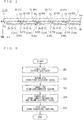
Fig. 3 is a flowchart illustrating a flow according to an example of a method for manufacturing a solar cell. -
Fig. 4 is a sectional view illustrating an example of an intermediate state of manufacturing of a solar cell. -
Fig. 5 is a sectional view illustrating an example of an intermediate state of the manufacturing of a solar cell. -
Fig. 6 is a sectional view illustrating an example of an intermediate state of the manufacturing of a solar cell. -
Fig. 7 is a sectional view illustrating an example of an intermediate state of the manufacturing of a solar cell. -
Fig. 8 is a sectional view illustrating an example of an intermediate state of the manufacturing of a solar cell. -
Fig. 9 is a sectional view illustrating an example of an intermediate state of the manufacturing of a solar cell. -
Fig. 10 is a sectional view illustrating an example of an intermediate state of the manufacturing of a solar cell. -
Fig. 11 is a sectional view illustrating a section of an example of a solar cell according to a second embodiment. -
Fig. 12 is a sectional view illustrating a section of an example of a solar cell according to a third embodiment. -
Fig. 13 is a sectional view illustrating a section of an example of a solar cell according to a fourth embodiment. -
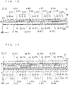
Fig. 14 is a sectional view illustrating a section of an example of a solar cell according to a fifth embodiment. -
Fig. 15 is a sectional view illustrating a configuration of an example of a solar cell. - As a thin film solar cell, for example, there is adopted a
solar cell 11 in which a plurality ofsolar cell elements 12 are arrayed on asubstrate 13, as illustrated inFig. 15 . Here, each of thesolar cell elements 12 has a structure in which afirst electrode layer 12a, asemiconductor layer 12b having a PN junction or a PIN junction, and asecond electrode layer 12c are laminated. In addition, thefirst electrode layer 12a and thesecond electrode layer 12c are electrically connected between thesolar cell elements 12 adjacent to each other, so that the adjacentsolar cell elements 12 are electrically connected in series. Specifically, between the adjacentsolar cell elements 12, there is provided a portion (also referred to as a connecting portion) 14 for electrically connecting thefirst electrode layer 12a to thesecond electrode layer 12c, for example. In addition, between the adjacentsolar cell elements 12, there are provided a region (also referred to as a first separation region) Da1 separating thefirst electrode layers 12a and a region (also referred to as a second separation region) Da2 separating thesecond electrode layers 12c, for example. - Between the connecting
portion 14 and the second separation region Da2, there may be provided a part Ds1 as a dead space in which while incident light is absorbed, photoelectric conversion in accordance with this incident light cannot be performed, resulting in no contribution to power generation. In other words, the dead space can be a region that does not utilize incident light. This dead space may be formed when the second separation region Da2 is formed by scribing or the like after thefirst electrode layer 12a, thesemiconductor layer 12b, and thesecond electrode layer 12c are laminated on thesubstrate 13, for example. Here, a dead space can be formed by forming the connectingportion 14 and the second separation region Da2 at respective positions separated from each other to prevent the connectingportion 14 from being scraped by scribing or the like, for example. - Thus, the inventors of the present invention have developed a technique capable of effectively utilizing incident light for a thin film solar cell.
- Herein after, various embodiments will be descri bed with reference to drawings. In the drawings, the same reference signs are assigned to portions having a similar configuration and function, thus, duplicated description thereof is eliminated in the following description. Each of the drawings is illustrated schematically. In each of
Figs. 1 and2 , and4 to 14 , a right handed X Y Z coordinate system is added. This X Y Z coordinate system includes +X direction that is a direction in which the plurality ofsolar cell elements 2 are arrayed, +Y direction that is a longitudinal direction of a third groove P3 located between the adjacentsolar cell elements 2, and +Z direction that is a direction orthogonal to both +X direction and +Y direction. - A
solar cell 1 according to a first embodiment will be described with reference toFigs. 1 and2 . - As illustrated in
Figs. 1 and2 , thesolar cell 1 includes asubstrate 3, a plurality ofsolar cell elements 2, a connectingportion 4, and atransparent portion 5, for example. In the first embodiment, a perovskite solar cell is adopted. - The
substrate 3 can support the plurality ofsolar cell elements 2 and protect the plurality ofsolar cell elements 2. When thesubstrate 3 has light transmittance to light having a wavelength in a specific range, light having transmitted through thesubstrate 3 can be incident on the plurality ofsolar cell elements 2, for example. As thesubstrate 3, a flat plate having a rectangular plate surface is adopted, for example. When a material such as glass, acrylic, or polycarbonate is adopted as a material of thesubstrate 3, thesubstrate 3 with light transmittance to light having a wavelength in a specific range can be fabricated. As the glass, a material with high light transmittance such as white sheet glass, tempered glass, and heat-ray reflective glass can be adopted, for example. In the present specification, light having a wavelength in a specific range means a wavelength in a range in which thesolar cell element 2 can perform photoelectric conversion. - The plurality of
solar cell elements 2 are arrayed in a planar manner along +X direction as a first direction. Here, the term, "arrayed in a planar manner", means that each of thesolar cell elements 2 is located along a virtual or actual plane, and the plurality ofsolar cell elements 2 are arrayed. In the first embodiment, the plurality ofsolar cell elements 2 are arrayed on a surface of thesubstrate 3. More specifically, the plurality ofsolar cell elements 2 includes fivesolar cell elements 2 arrayed along the first direction (+X direction) on thesubstrate 3. The fivesolar cell elements 2 includes a firstsolar cell element 21, a secondsolar cell element 22, a thirdsolar cell element 23, a fourthsolar cell element 24, and a fifthsolar cell element 25, being arrayed in order in +X direction. In other words, the plurality ofsolar cell elements 2 includes the n-th solar cell element 2n (n is a natural number of 1 to 5). - In the first embodiment, each of the
solar cell elements 2 has a strip-like shape with a longitudinal direction as +Y direction. Each of thesolar cell elements 2 includes afirst electrode layer 2a, asemiconductor layer 2b, and asecond electrode layer 2c. When at least one of thefirst electrode layer 2a and thesecond electrode layer 2c has higher light transmittance to light having a wavelength in a specific range than that of thesemiconductor layer 2b, for example, incident light may pass through at least one of thefirst electrode layer 2a and thesecond electrode layer 2c in each of thesolar cell elements 2. As a result, thesemiconductor layer 2b can be irradiated with the incident light. - The
first electrode layer 2a is located on thesubstrate 3. In other words, thefirst electrode layer 2a is located closer to thesubstrate 3 than the secondel ectrode layer 2c. Thefirst electrode layer 2a can collect electric charges generated by photoelectric conversion in accordance with light irradiation on thesemiconductor layer 2b. When thesubstrate 3 has light transmittance, for example, thefirst electrode layer 2a with higher light transmittance to light having a wavelength in a specific range than that of thesemiconductor layer 2b allows the light having a wavelength in the specific range to enter thesemiconductor layer 2b through thesubstrate 3 and thefirst electrode layer 2a, for example. This enables fabricating thesolar cell 1 in which thesubstrate 3 with light transmittance constitutes a front surface as a light receiving surface of thesolar cell 1. - Specifically, when a transparent conductive oxide (TCO) with light transmittance to light having a wavelength in a specific range is adopted as a material of the
first electrode layer 2a, the light having a wavelength in the specific range can enter thesemiconductor layer 2b through thesubstrate 3 and thefirst electrode layer 2a, for example. The transparent conductive oxide may include indium tin oxide (ITO), fluorine-doped tin oxide(FTO), zinc oxide (ZnO), or the like, for example. - In the first embodi ment, the five
first electrode layers 2a are arrayed in a planar manner on thesubstrate 3 in order in +X direction. Here, thefirst electrode layer 2a of the m-th solar cell element 2m (m is a natural number of 1 to 4) and thefirst electrode layer 2a of the (m+1)-th solar cell element 2 (m+1) are juxtaposed so as to sandwich a gap (referred to also as a first gap) G1. For example, thefirst electrode layer 2a of the firstsolar cell element 21 and thefirst electrode layer 2a of the secondsolar cell element 22 are juxtaposed so as to sandwich the gap (referred to also as the first gap) G1. Each first gap G1 has a longitudinal direction along +Y direction. In addition, there is provided a first groove P1 with a bottom surface formed by thesubstrate 3 and two side surfaces formed by respective end surfaces of the twofirst electrode layers 2a sandwiching the first gap G1, the end surfaces facing each other. - The
semiconductor layer 2b is interposed between thefirst electrode layer 2a and thesecond electrode layer 2c. Thesemiconductor layer 2b of the m-th solar cell element 2m is located on an end portion in -X direction of thefirst electrode layer 2a of the (m+1)-th solar cell element 2 (m+1) adjacent in +X direction. For example, thesemiconductor layer 2b of the firstsolar cell element 21 is located on an end portion in -X direction of thefirst electrode layer 2a of the secondsolar cell elements 22 adjacent in +X di recti on. - The
semiconductor layer 2b has a structure in which a layer (perovskite semiconductor layer) of a semiconductor having a perovskite structure (referred to also as a perovskite semiconductor) and a hole transport layer (HTL) are laminated, for example. When thesemiconductor layer 2b is a perovskite semiconductor, light having a wavelength in a specific range includes visible light and infrared light. - The perovskite semiconductor may include a halide-based organic-inorganic perovskite semiconductor, for example. The halide-based organic-inorganic perovskite semiconductor can be made of organic perovskite such as CH3NH3PbI3, for example. The organic perovskite can be formed by applying a raw material liquid on the
first electrode layer 2a located on thesubstrate 3 and drying it, for example. The organic perovskite is here a thin film having crystallinity. At this time, the first gap G1 is also filled with the raw material liquid, and a part of the perovskite semiconductor can be formed in the first gap G1 by drying, for example. The raw material liquid can be produced by dissolving halogenated alkylamine and lead halidethat are raw materials in a solvent, for example. - The hole transporting layer (HTL) can collect and output positive holes. As a material of the hole transporting layer (HTL), spiro-OMeTAD that is a soluble diamine derivative or the like is adopted, for example.
- When the perovskite semiconductor is an intrinsic semiconductor (i-type semiconductor), the hole transport layer is a p-type semiconductor, and the TCO constituting the
first electrode layer 2a is an n-type semiconductor, for example, a PIN junction region can be formed. In the PIN junction region, power generation can be performed by photoelectric conversion in accordance with light irradiation. In thesemiconductor layer 2b, a layer of an n-type semiconductor may be interposed between the perovskite semiconductor layer and thefirst electrode layer 2a, for example. At this time, the PIN junction region can be formed only in thesemi conductor layer 2b. - The
second electrode layer 2c is located on thesemiconductor layer 2b. Thesecond electrode layer 2c can collect electric charges generated by photoelectric conversion in accordance with light irradiation on thesemiconductor layer 2b. When thesecond electrode layer 2c has higher light transmittance to light having a wavelength in a specific range than that of thesemiconductor layer 2b, for example, light incident from a side opposite to thesubstrate 3 may enter thesemiconductor layer 2b by passing through thesecond electrode layer 2c, for example. This enables fabricating thesolar cell 1 with both surfaces in, Z direction that are each a light receiving surface. As a result, incident light to thesolar cell 1 can be effectively used. - Specifically, when a transparent conductive oxide (TCO) with light transmittance to light having a wavelength in a specific range is adopted as a material of the
second electrode layer 2c, for example, the light having a wavelength in the specific range can enter thesemiconductor layer 2b through thesecond electrode layer 2c. The transparent conductive oxide may include indium tin oxide (ITO), fluorine-doped tin oxide (FTO), zinc oxide (ZnO), or the like, for example. - In the first embodi ment, the five second electrode layers 2c are arrayed in order in +X direction in a planar manner. Here, the
second electrode layer 2c of the m-th solar cell element 2m and thesecond electrode layer 2c of the (m+1)-th solar cell element 2 (m+1) are juxtaposed so as to sandwich a gap (referred to also as a second gap) G2. For example, thesecond electrode layer 2c of the firstsolar cell element 21 and thesecond electrode layer 2c of the secondsolar cell element 22 are juxtaposed so as to sandwich the gap (second gap) G2. Each second gap G2 has a longitudinal direction along +Y direction, for example. In addition, a third groove P3 with a bottom surface formed by thefirst electrode layer 2a is formed. In each of thesolar cell elements 2, thesecond electrode layer 2c extends more in the +X direction than thefirst electrode layer 2a. In other words, the second gap G2 is provided at a position shifted in the first direction (+X di recti on) from the first gap G1. - The connecting
portion 4 electrically connects two adjacentsolar cell elements 2 among the plurality ofsolar cell elements 2 in series. In the first embodiment, the m-th connecting portion 4m electrically connects the m-th solar cell element 2m to the (m+1)-th solar cell element 2 (m+1). For example, the first connectingportion 41 electrically connects the firstsolar cell element 21 to the secondsolar cell element 22. More specifically, the m-th connecting portion 4m electrically connects thesecond electrode layer 2c of the m-th solar cell element 2m to thefirst electrode layer 2a of the (m+1)-th solar cell element 2 (m+1). For example, the first connectingportion 41 electrically connects thesecond electrode layer 2c of the firstsolar cell element 21 to thefirst electrode layer 2a of the secondsolar cell element 22. This enables the plurality ofsolar cell elements 2 to be electrically connected in series. - The connecti ng
portion 4 is located between thesemiconductor layer 2b and thetransparent portion 5 in +X direction. In other words, there is provided a second groove P2 having side surfaces formed by the corresponding one of an end surface in +X direction of thesemiconductor layer 2b and an end surface in -X direction of thetransparent portion 5, and a bottom surface formed by a surface of thefirst electrode layer 2a in -Z direction. The second groove P2 has a longitudinal direction along +Y direction. Then, the connecti ngportion 4 is filled in the second groove P2, for example. - The
transparent portion 5 has higher light transmittance to light having a wavelength in a specific range than that of thesemiconductor layer 2b. Thetransparent portion 5 can be formed by locally heating a part of the perovskite semiconductor layer, for example. - In the first embodiment, the m-th transparent portion 5m is located between the m-th connecting portion 4m of the m-th solar cell element 2m and the (m+1)-th solar cell element 2 (m+1). For example, the first
transparent portion 51 is located between the first connectingportion 41 of the firstsolar cell element 21 and the secondsolar cell element 22. More specifically, the m-th transparent portion 5m is provided at a position shifted in the first direction (+X direction) from the m-th connecting portion 4m, between thesecond electrode layer 2c of the m-th solar cell element 2m and thefirst electrode layer 2a of the (m+1)-th solar cell element 2 (m+1). For example, the firsttransparent portion 51 is provided at a position shifted in the first direction (+X direction) from the first connectingportion 41, between thesecond electrode layer 2c of the firstsolar cell element 21 and the first electrode layer 2a of the secondsolar cell element 22. Providi ng thetransparent portion 5 as described above enables reducing a dead space in which while incident light is absorbed, photoelectric conversion in accordance with this incident light cannot be performed, resulting in no contribution to power generation, for example. As a result, incident light can be effectively used. - In the first
solar cell element 21, thefirst electrode layer 2a includes a portion (referred to also as a first extension) 2ae extending in -X direction from thesemiconductor layer 2b and thesecond electrode layer 2c. In the fifthsolar cell element 25, thesemiconductor layer 2b and thesecond electrode layer 2c extend in +X direction from thefirst electrode layer 2a. In addition, there is provided a portion (referred to also as a second extension) 2ce that extends in +X direction from thefirst electrode layer 2a and thesemi conductor layer 2b. Onto the first extension 2ae, a first conductor W1 for output of a first polarity is electrically connected. Onto the second extension 2ce, a second conductor W2 for output of a second polarity is electrically connected. For example, when the first polarity is a negative polarity, the second polarity is a positive polarity. For example, when the first polarity is a positive polarity, the second polarity is a negative polarity. - Next, a method for manufacturing a
solar cell 1 will be described with reference toFigs. 3 to 10 . - As illustrated in
Fig. 3 , thesolar cell 1 can be manufactured by performing first step ST1 to fifth step ST5 in this order, for example. - In first step ST1, a
substrate 3 is prepared as illustrated inFig. 4 , for example. As thesubstrate 3, a flat plate with light transmittance to light having a wavelength in a specific range and with a rectangular plate surface is adopted, for example. - In second step ST2, a plurality of
first electrode layers 2a arrayed in the first direction (+ X direction) in a planar manner is formed on a surface of thesubstrate 3. - As illustrated in
Fig. 5 , an electrode layer 2a0 is first formed on one plate surface of thesubstrate 3. The electrode layer 2a0 can be formed by sputteri ng or vapor deposition, for example. The electrode layer 2a0 can be made of a transparent conductive oxide such as ITO, FTO, or ZnO, for example. At this time, the electrode layer 2a0 may be set to have a thickness of about 10 nm to 1000 nm, for example. - Next, the electrode layer 2a0 is separated into a plurality of
first electrode layers 2a as illustrated inFig. 6 . For example, the plurality offirst electrode layers 2a is formed by forming a plurality of first grooves P1 (first gaps G1). This forms first to fifthfirst electrode layers 2a arrayed in the first direction (+X direction) in a planar manner on the surface of thesubstrate 3, for example. The plurality of first grooves P1 (first gaps G1) can be formed by irradiating a region of a desired pattern in the electrode layer 2a0 with a laser, for example. Each of the first grooves P1 (each of the first gaps G1) can be formed so as to have a longitudinal direction as +Y direction. Each of the first grooves P1 (each of the first gaps G1) is set to have a width of about 30 mm to 300 mm, for example. In addition, each of thefirst electrode layers 2a is set to have a width of about 1 mm to 10 mm in the first direction (+ X direction), for example. The first groove P1 (fi rst gap G 1) may be formed by scri bi ng, for example. - In third step ST3, a semiconductor region 2b0 for a perovskite solar cell is formed on each of the
first electrode layers 2a as illustrated inFig. 7 . For example, the plurality offirst electrode layers 2a includes thefirst electrode layers 2a arrayed first to fifth. - The semiconductor region 2b0 can be formed by coating and drying a raw material liquid, for example. The semiconductor region 2b0 has a structure in which a plurality of layers including a perovskite semiconductor layer and a hole transport layer are laminated. In this case, after the perovskite semiconductor layer is formed by applying and drying a first raw material liquid, the hole transport layer can be formed on the perovskite semiconductor layer by coating and drying a second raw material liquid, for example. At this time, the semiconductor region 2b0 may be set to have a thickness of about 100 nm to 2000 nm, for example.
- At this time, the semiconductor region 2b0 also enters the plurality of first grooves P1 (first gaps G1). In the first embodiment, the semiconductor region 2b0 is separated into a plurality of
semiconductor layers 2b, as illustrated inFig. 8 . For example, forming a plurality of second grooves P2 forms a plurality ofsemiconductor layers 2b. This forms the semiconductor layers 2b arrayed first to fifth in the first direction (+X direction) in a planar manner on the plurality offirst electrode layers 2a, for example. In the first direction (+X direction), the m-th second groove P2 can be formed by scribing or the like in a region of a desired pattern at a position shifted in the +X direction from the m-th first groove P1 in the semiconductor region 2b0. At this time, the m-th second groove P2 is formed so as to be separated from the m-th first groove P1 in +X di recti on by about 10 mm to 100 mm, for example. Each of the second grooves P2 can be formed so as to have a longitudinal di recti on as +Y di recti on. Then, each of the second grooves P2 is set to have a width of about 30 mm to 300 mm, for example. - In fourth step ST4, a connecting
portion 4 and asecond electrode layer 2c are formed. - As illustrated in
Fig. 9 , an electrode layer 2c0 is first formed on the semiconductor region 2b0. The electrode layer 2c0 can be formed by sputtering, vapor deposition, or the like, for example. The electrode layer 2c0 can be made of a transparent conductive oxide such as ITO, FTO, or ZnO, for example. The electrode layer 2c0 can be set to have a thickness of about 10 nm to 1000 nm, for example. At this time, the electrode layer 2c0 enters each of the second grooves P2 in the semiconductor region 2b0. This forms a first connectingportion 41, a second connectingportion 42, a third connectingportion 43, and a fourth connectingportion 44. In other words, there is formed the m-th connecting portion 4m located at a gap (second groove P2) between the m-th semiconductor layer 2b and the (m+1)-th semiconductor layer 2b in the first direction (+X direction) in the semiconductor region 2b0. At this time, the m-th connecting portion 4m is electrically connected to the (m+1)-thfirst electrode layer 2a. For example, the first connectingportion 41 is electrically connected to thefirst electrode layer 2a arrayed second. - Next, the electrode layer 2c0 is separated into a plurality of second electrode layers 2c as illustrated in
Fig. 10 . For example, the plurality ofsecond electrode layers 2c is formed by forming a plurality of third grooves P3 (second gaps G2). This forms the first to fifth second electrode layers 2c arrayed along the first direction (+X direction) in a planar manner on the first tofifth semiconductor layers 2b arrayed along the first direction (+X direction) in a planar manner, for example. Specifically, the m-thsecond electrode layer 2c is located on the m-th semiconductor layer 2b. For example, the firstsecond electrode layer 2c is located on the firstsemi conductor layer 2b. Then, the m-thsecond electrode layer 2c is electrically connected to the m-th connecting portion 4m. For example, the firstsecond electrode layer 2c is electrically connected to the first connectingportion 41. - Here, the m-th third groove P3 (second gap G2) can be formed by scribing or the like in a region of a desired pattern at a position shifted in +X direction from the m-th second groove P2 in the semiconductor region 2b0, for example. At this time, the m-th third groove P3 is formed so as to be separated from the m-th second groove P2 in +X di recti on by about 10 mm to 100 mm, for example. Each of the third grooves P3 (each of the second gaps G2) is set to have a width of about 10 mm to 100 mm, for example. As a result, each of the
second electrode layers 2c has a width of about 1 mm to 10 mm in the first direction (+X direction), for example. Then, the m-th third groove P3 (second gap G2) in the first direction (+X direction) is located at a position shifted in the first direction (+X direction) from the m-th first gap G1 and the m-th connecting portion 4m in the first direction (+X direction). At this time, an m-th part Ds1 to be a dead space of the semiconductor region 2b0 can be formed between the m-th connecting portion 4m and the m-th third groove P3 (second gap G2). In this case, the m-thsecond electrode layer 2c is located from a portion on the m-th semiconductor layer 2b to a portion on the m-th part Ds1. - In fifth step ST5, the part Ds1 to be a dead space of the semiconductor region 2b0 is heated to form a
transparent portion 5 having enhanced light transmittance to light having a wavelength in a specific range in the part Ds1. Here, the m-th part Ds1 located on the (m+1)-thfirst electrode layer 2a in the semiconductor region 2b0 is heated to form thetransparent portion 5 with the m-th part that has higher light transmittance to light having a wavelength in the specific range than that of the semiconductor region 2b0, for example. The heating of the part Ds1 can be performed by local laser irradiation, for example. - In this case, a band gap of a perovskite semiconductor constituting the part Ds1 is increased by being heated at a relatively low temperature of 100·C to 200·C with a laser, for example. As a result, the perovskite semiconductor can be changed to a wide-gap semiconductor that has higher light transmittance to light having a wavelength in the specific range than that of the original perovskite semiconductor. As a material of a perovskite semiconductor with light transmittance to light having a wavelength in a specific range to be improved in accordance with heating as described above, a perovskite semiconductor having a Pb-I bond such as CH3NH3PbI3, CsPbI3, and NH2CHNH2PbI3 is conceivable, for example. It is conceivable that the Pb-I bond of the perovskite semiconductor is changed in state due to structural change by heating to increase the band gap. In addition, a hole transport layer constituting the part Ds1 can be made of a material with high light transmittance to light having a wavelength in a specific range. This enables the part Ds1 serving as a dead space to be made transparent by heating at a relatively low temperature with small energy applied.
- Specifically, a compound having a perovskite type crystal structure or a crystal structure similar to this crystal structure is represented by the general formula such as ABX3, A2BX4, AB'X4, and A'BX4. Here, A represents a monovalent cation such as CH3NH3 +, CH (NH2)2 +, and Cs+. A' and B each represents divalent a cation such as Pb2+, and Sn2+. B' represents a trivalent cation such as Bi3+, and Sb3+. X represents a monovalent anion such as Cl-, Br, and I-.
- Then, these compounds generate decomposition according to reaction formulas (1) to (4) by heating, for example.


- When a perovskite semiconductor is made transparent by laser irradiation, the laser is set to have an output of about 0.1 W to 1 W, for example. A laser beam is set to have a wavelength of light of about 400 nm to 700 nm, for example. The laser beam is set to have a diameter of light flux of about 40 mm, for example. The laser beam is set to have a scanning speed of 1200 mm/sec, for example. Light having a wavelength of 400 nm to 700 nm is not absorbed by a TCO and can be absorbed by a perovskite semiconductor. This enables the perovskite semiconductor to be local ly heated.
- Forming the
transparent portion 5 as described above enables reducing a dead space in which while incident light is absorbed, photoelectric conversion in accordance with this incident light cannot be performed, resulting in no contribution to power generation, for example. As a result, incident light can be effectively used. - In the
solar cell 1 according to the first embodiment, providing thetransparent portion 5 enables reducing a dead space in which while incident light is absorbed, photoelectric conversion in accordance with this incident light cannot be performed, resulting in no contribution to power generation, for example. As a result, incident light can be effectively used. - For example, when the
transparent portion 5 provided reduces the dead space, a part of the incident light lost due to existence of the dead space can be easily emitted from a back surface of thesolar cell 1, being a non-light receiving surface. This enables a see-through solar cell with much transmitted light and excellent appearance to be fabricated, for example. - The present disclosure is not limited to the first embodiment described above, and various modifications and improvements are possible without departing from the essence of the present disclosure.
- In the first embodiment above, the
substrate 3 may be located not on a front surface side but on a back surface side, as illustrated inFig. 11 , for example. Asolar cell 1A according to the second embodiment illustrated inFig. 11 has an upside-down structure of thesolar cell 1 accordi ng to the fi rst embodi ment illustrated inFig. 2 . - The
solar cell 1A accordi ng to the second embodi ment here includes asubstrate 3, for example. Here, a plurality ofsolar cell elements 2 are arrayed on thesubstrate 3 along a surface thereof. Afirst electrode layer 2a is located closer to thesubstrate 3 than asecond electrode layer 2c. Thesecond electrode layer 2c has higher light transmittance to light having a wavelength in a specific range than that of thesemiconductor layer 2b. When structure as described above is adopted, incident light can be effectively used in thesolar cell 1A with a front surface as a light receiving surface, on an opposite side of thesubstrate 3, for example. - In each of the first and second embodiments described above, there may be provided a reflecting portion for reflecting light having a wavelength in a specific range that has passed through the
transparent portion 5 to enable the light to enter thesemiconductor layer 2b, for example. In other words, there may be provided a reflecting portion capable of reflecting light having a wavelength in a specific range that has passed through thetransparent portion 5, on a virtual straight line passing through a part of afirst electrode layer 2a and a part of asecond electrode layer 2c located so as to sandwich thetransparent portion 5. When structure as described above is adopted, light having passed through thetransparent portion 5 can be reflected by the reflecting portion to enable the light to enter thesemiconductor layer 2b, for example. At this time, the light reflected by the reflecting portion can be used for photoelectric conversion in thesemiconductor layer 2b. As a result, incident light can be effectively used. - For example, when a metal without light transmittance to light having a wavelength in a specific range is adopted as the material of the
second electrode layer 2c in the first embodiment, thesecond electrode layer 2c can serve as an electrode layer (referred to also as a metal electrode layer) as a reflecting portion capable of reflecting light having a wavelength in a specific range, having passed through thetransparent portion 5. In addition, for example, when a metal without light transmittance to light having a wavelength in a specific range is adopted as the material of thefirst electrode layer 2a in the second embodiment, thefirst electrode layer 2a can serve as a metal electrode layer as a reflecting portion capable of reflecting light having a wavelength in the specific range, having passed through thetransparent portion 5. In other words, it is conceivable that one of thefirst electrode layer 2a and thesecond electrode layer 2c may be a metal electrode layer capable of reflecting light having a wavelength in the specific range that has passed through thetransparent portion 5. - As a material of the metal electrode layer, a metal material excellent in conductivity and light reflection characteristics, such as aluminum, can be adopted, for example. In this case, at least a part of light having a wavelength in a specific range that has passed through the
transparent portion 5 can be reflected by a surface of the metal electrode layer to enable the light to enter thesemiconductor layer 2b, for example. At this time, the light reflected by the metal electrode layer can be used for photoelectric conversion in thesemiconductor layer 2b, for example. As a result, incident light to thesolar cells transparent portion 5 to allow the light to enter thesemiconductor layer 2b does not become a large scale and can be easily fabricated, for example. - For example, when the
second electrode layer 2c has higher light transmittance to light having a wavelength in a specific range than that of thesemiconductor layer 2b in the first embodiment, a reflecting portion for reflecting light may be added on a back surface side as a non-receiving surface. As illustrated inFig. 12 , there may be adopted asolar cell 1B to which a reflecting portion Bs1 capable of scattering light by diffusely reflecting light, such as a white back sheet, is added, for example. At this time, it is sufficient that the reflecting portion Bs1 is supported by a sealingmaterial 6 such as ethylene vinyl acetate copolymer (EVA), for example. Structure as described above allows a part of incident light that is previously lost due to existence of a dead space to pass through thetransparent portion 5 in accordance with decrease in the dead space. Then, light having passed through thetransparent portion 5 can be reflected by the reflecting portion Bs1 to enter thesemiconductor layer 2b, for example. At this time, the light can be absorbed in a region on a back surface side of thesemiconductor layer 2b in thesolar cell 1. A part of the light absorbed here can be used for photoelectric conversion. As a result, incident light can be effectively used. - As illustrated in
Fig. 13 , there may be adopted asolar cell 1C where thesubstrate 3 includes a portion (referred to also as a reflecting portion) Mr1 that reflects light against light irradiation from a +Z side in the second embodiment above, for example. Structure as described above allows a part of incident light that is previously lost due to existence of a dead space to pass through thetransparent portion 5 in accordance with decrease in the dead space. Then, light having passed through thetransparent portion 5 is reflected by the reflecting portion Mr1 to enable the light to be absorbed in a region on the back surface side of thesemiconductor layer 2b in thesolar cell 1. A part of the incident light absorbed here can be used for photoelectric conversion. As a result, incident light can be effectively used. - In each of the first and second embodiments, there may be provided one or more kinds of another solar cell element Sc1 different from the plurality of
solar cell elements 2 to receive light having passed through the plurality ofsolar cell elements 2 arrayed in a planar manner, for example. As illustrated inFig. 14 , there may be adopted asolar cell 1D including one or more kinds of another solar cell element Sc1 different from the plurality ofsolar cell elements 2 on a virtual straight line passing through a part of afirst electrode layer 2a and a part of asecond electrode layer 2c located so as to sandwich atransparent portion 5, for example. In this case, in each of thefirst electrode layer 2a and thesecond electrode layer 2c, it is sufficient that light transmittance to light having a wavelength in a specific range is higher than that of asemiconductor layer 2b, for example. For example, it is sufficient that thefirst electrode layer 2a and thesecond electrode layer 2c are made of a material such as a TCO having higher light transmittance to light having a wavelength in a specific range than that of thesemiconductor layer 2b. - Here, the plurality of
solar cell elements 2 as top cells absorbs visible light and near infrared light to use the light for photoelectric conversion, for example. In this case, it is conceivable that another solar cell element Sc1 constituting a bottom cell may absorb infrared light having a longer wavelength than that of near infrared light to use the light for photoelectric conversion, for example. As the other solar cell element Sc1, a solar cell element having a semiconductor layer made of silicon crystal is conceivable, for example. - When the
solar cell 1D above of a tandem type is adopted, light having passed through thetransparent portion 5 can be used for photoelectric conversion in another solar cell element Sc1, thereby enabling increase in the amount of power generation due to effective use of incident light, for example. As a result, conversion efficiency may increase. - In each of the first embodiment, the second embodiment, the third embodiment, and the fourth embodiment, described above, the part Ds1 of the semiconductor region 2b0 or a part correspondi ng to the part Ds1 may be made transparent by heati ng at certain timing after the semiconductor region 2b0 is formed, for example. When the part Ds1 of the semiconductor region 2b0 is made transparent by heating after the third groove P3 is formed in the semiconductor region 2b0, for example, the
semiconductor layer 2b constituting thesolar cell element 2 is less likely to deteriorate. - In each of the fi rst embodi ment, the second embodi ment, the third embodi ment, and the fourth embodiment, described above, the part Ds1 of the semiconductor region 2b0 may be heated by irradiation with infrared light in the shape of a slit, contact with a heated wire or a member in the shape of a blade, or the like, instead of irradiation with a laser beam, for example.
- In each of the first embodiment, the second embodiment, the third embodiment, and the fourth embodiment, described above, the plurality of second electrode layers 2c each may be formed in a form in which the third groove P3 (second gap G2) is previously formed by patterning with vapor deposition or the like using a mask or the like, for example. When structure as described above is adopted, the third grooves P3 (second gap G2) only needs to separate the plurality of second electrode layers 2c from each other, and may not reach the semiconductor region 2b0, for example. This enables a step of scribing the electrode layer 2c0 and the semiconductor region 2b0 to be eliminated, for example.
- In each of the first embodiment, the second embodi ment, the third embodiment, and the fourth embodiment, described above, the plurality of
semiconductor layers 2b each may be formed in a form in which the second groove P2 is previously formed by patterning with a coating method or the like using a mask or the like, for example. In this case, a step of forming the second groove P2 with scribing or the like after the semiconductor region 2b0 is formed can be eliminated. - In the
solar cells solar cell elements 2 may be arrayed in a planar manner, or two or more and four or lesssolar cell elements 2 may be arrayed in a planar manner, for example. - It is needless to say that all or a part of each of the embodiments described above can be combined as appropriate within a consistent range.
-
- 1, 1A, 1B, 1C, 1D, 11: solar cell
- 2, 12: solar cell element
- 2a, 12a: first electrode layer
- 2a0: electrode layer
- 2b, 12b: semiconductor layer
- 2b0: semiconductor region
- 2c, 12c: second electrode layer
- 2c0: electrode layer
- 2m: m-th solar cell element
- 2n: n-th solar cell element
- 3, 13: substrate
- 4. 14: connecting portion
- 4m: m-th connecting portion
- 21: first solar cell element
- 22: second solar cell element
- 23: third solar cell element
- 24: fourth solar cell element
- 25: fifth solar cell element
- 41: first connecti ng porti on
- 42: second connecting portion
- 43: third connecting portion
- 44: fourth connecting portion
- 5: transparent portion
- 5m: m-th transparent portion
- Bs1: reflecting portion
- Ds1: a part (dead space)
- G1: first gap
- G2: second gap
- Mr1: reflecting portion
- P1: first groove
- P2: second groove
- P3: third groove
- Sc1: another solar cell element
Claims (7)
- A solar cell comprising:a plurality of solar cell elements that are arrayed in a planar manner along a first direction, and include a first solar cell element and a second solar cell element that are adjacent to each other;a connecting portion that electrically connects the first solar cell element to the second solar cell element; anda transparent portion that is located between the connecting portion and the second solar cell element, whereineach of the solar cell elements includes a first electrode layer, a second electrode layer, and a semiconductor layer interposed between the fi rst electrode layer and the second electrode layer,the first electrode layer of the first solar cell element and the first electrode layer of the second solar cell element are juxtaposed so as to sandwich a first gap,the second electrode layer of the first solar cell element and the second electrode layer of the second solar cell element are juxtaposed so as to sandwich a second gap,the second gap is provided at a position shifted in the first direction from the first gap,the connecting portion electrically connects the second electrode layer of the first solar cell element to the first electrode layer of the second solar cell element,the transparent portion is provided between the second electrode layer of the first solar cell element and the first electrode layer of the second solar cell element at a position shifted in the first direction from the connecting portion, and has higher light transmittance than that of the semiconductor layer, andat least one of the first electrode layer and the second electrode layer has higher light transmittance than that of the semiconductor layer.
- The solar cell according to claim 1, further comprising a substrate with light transmittance, wherein
the plurality of solar cell elements are arrayed on the substrate along a surface of the substrate, and
the first electrode layer is located closer to the substrate than the second electrode layer and has higher light transmittance than that of the semiconductor layer. - The solar cell according to claim 1, further comprising a substrate, wherein
the plurality of solar cell elements are arrayed on the substrate along a surface of the substrate,
the first electrode layer is located closer to the substrate than the second electrode layer, and
the second electrode layer has higher light transmittance than that of the semiconductor layer. - The solar cell according to any one of claims 1 to 3, further comprising one or more kinds of solar cell element different from the plurality of solar cell elements that is provided on a virtual straight line passing through a part of the first electrode layer and a part of the second electrode layer located so as to sandwich the transparent portion, wherein
each of the first electrode layer and the second electrode layer has higher light transmittance than that of the semiconductor layer. - The solar cell according to any one of claims 1 to 3, further comprising a reflection portion capable of reflecting light having passed through the transparent portion that is provided on a virtual straight line passing through a part of the first electrode layer and a part of the second electrode layer located so as to sandwich the transparent portion.
- The solar cell according to any one of claims 1 to 3, and 5, wherein any one of the first electrode layer and the second electrode layer includes a metal electrode layer capable of reflecting light having passed through the transparent portion.
- A method for manufacturing a solar cell, the method comprising:preparing a substrate;forming a first electrode layer arrayed first, and a first electrode layer arrayed second, on a surface of the substrate along a first direction in a planar manner;forming a semiconductor region for a perovskite solar cell on the first electrode layer arrayed fi rst, and the fi rst electrode layer arrayed second; andforming a connecting portion located in a gap between a semiconductor layer arrayed first and a semiconductor layer arrayed second in a planar manner along the first direction in the semiconductor region while being electrically connected to the first electrode layer arrayed second, and a second electrode layer located on the semiconductor layer arrayed fi rst while being electrically connected to the connecting portion, whereina part of the semiconductor region, located on the first electrode layer arrayed second is heated, after the semiconductor region is formed, to increase light transmittance of the part.
Applications Claiming Priority (2)
| Application Number | Priority Date | Filing Date | Title |
|---|---|---|---|
| JP2016169204 | 2016-08-31 | ||
| PCT/JP2017/031359 WO2018043644A1 (en) | 2016-08-31 | 2017-08-31 | Solar cell and method of manufacturing solar cell |
Publications (2)
| Publication Number | Publication Date |
|---|---|
| EP3509118A1 true EP3509118A1 (en) | 2019-07-10 |
| EP3509118A4 EP3509118A4 (en) | 2020-04-22 |
Family
ID=61309392
Family Applications (1)
| Application Number | Title | Priority Date | Filing Date |
|---|---|---|---|
| EP17846648.8A Pending EP3509118A4 (en) | 2016-08-31 | 2017-08-31 | SOLAR CELL AND MANUFACTURING METHOD OF SOLAR CELL |
Country Status (5)
| Country | Link |
|---|---|
| US (1) | US11011718B2 (en) |
| EP (1) | EP3509118A4 (en) |
| JP (1) | JP6745345B2 (en) |
| CN (1) | CN109643764B (en) |
| WO (1) | WO2018043644A1 (en) |
Cited By (1)
| Publication number | Priority date | Publication date | Assignee | Title |
|---|---|---|---|---|
| WO2022200898A1 (en) * | 2021-03-22 | 2022-09-29 | Ricoh Company, Ltd. | Photoelectric conversion element, photoelectric conversion module, electronic device, and power supply module |
Families Citing this family (8)
| Publication number | Priority date | Publication date | Assignee | Title |
|---|---|---|---|---|
| WO2019138095A1 (en) * | 2018-01-12 | 2019-07-18 | Katholieke Universiteit Leuven | Modified perovskites and perovskite likes and uses thereof |
| CN112352327B (en) * | 2019-03-19 | 2024-06-11 | 株式会社东芝 | Photoelectric conversion element and method for manufacturing the same |
| WO2020188777A1 (en) * | 2019-03-19 | 2020-09-24 | 株式会社 東芝 | Photoelectric conversion element and method for manufacturing photoelectric conversion element |
| KR102636393B1 (en) * | 2019-07-16 | 2024-02-13 | 가부시키가이샤 리코 | Solar modules, electronics, and power modules |
| CN111463315B (en) * | 2019-08-26 | 2021-08-20 | 杭州纤纳光电科技有限公司 | A kind of solar cell cutting and passivation integrated processing method and solar cell |
| JP7600618B2 (en) * | 2020-02-27 | 2024-12-17 | 株式会社リコー | Photoelectric conversion element and photoelectric conversion module |
| CN116367564A (en) * | 2021-12-24 | 2023-06-30 | 宁德时代新能源科技股份有限公司 | Solar cell, manufacturing method thereof, photovoltaic module and electricity utilization device |
| CN118338690B (en) * | 2024-06-14 | 2024-11-08 | 江苏汇显显示技术有限公司 | Solar cell module, preparation method thereof and solar cell |
Family Cites Families (12)
| Publication number | Priority date | Publication date | Assignee | Title |
|---|---|---|---|---|
| JP2000036602A (en) * | 1998-07-17 | 2000-02-02 | Sony Corp | Thin film transistor, method of manufacturing the same, and display device |
| JP4439492B2 (en) | 2006-05-25 | 2010-03-24 | 本田技研工業株式会社 | Chalcopyrite solar cell and method for manufacturing the same |
| DE102007005091B4 (en) * | 2007-02-01 | 2011-07-07 | Leonhard Kurz GmbH & Co. KG, 90763 | solar cell |
| DE102007021843A1 (en) | 2007-05-07 | 2008-11-13 | Leonhard Kurz Gmbh & Co. Kg | Photovoltaic module |
| WO2011052582A1 (en) | 2009-10-29 | 2011-05-05 | 住友化学株式会社 | Method for manufacturing organic thin-film solar battery module |
| JP2013219064A (en) * | 2010-08-05 | 2013-10-24 | Mitsubishi Electric Corp | Photoelectric conversion device manufacturing method |
| US9076768B2 (en) * | 2011-05-16 | 2015-07-07 | Georgia Tech Research Corporation | Systems and methods for producing low work function electrodes |
| JP2013055216A (en) * | 2011-09-05 | 2013-03-21 | Dainippon Printing Co Ltd | Solar cell and solar cell module |
| KR101283113B1 (en) * | 2011-12-09 | 2013-07-05 | 엘지이노텍 주식회사 | Solar cell module and manufacturing method thereof |
| US20160005987A1 (en) * | 2014-07-01 | 2016-01-07 | Sharp Laboratories Of America, Inc. | Planar Structure Solar Cell with Inorganic Hole Transporting Material |
| WO2016017617A1 (en) * | 2014-07-29 | 2016-02-04 | 京セラ株式会社 | Photoelectric conversion device, tandem photoelectric conversion device, and photoelectric conversion device array |
| CN104979477A (en) * | 2015-05-18 | 2015-10-14 | 常州天合光能有限公司 | Z type serial perovskite solar cell assembly and preparation method therefor |
-
2017
- 2017-08-31 WO PCT/JP2017/031359 patent/WO2018043644A1/en not_active Ceased
- 2017-08-31 JP JP2018537397A patent/JP6745345B2/en active Active
- 2017-08-31 EP EP17846648.8A patent/EP3509118A4/en active Pending
- 2017-08-31 CN CN201780052889.XA patent/CN109643764B/en active Active
- 2017-08-31 US US16/328,181 patent/US11011718B2/en active Active
Cited By (2)
| Publication number | Priority date | Publication date | Assignee | Title |
|---|---|---|---|---|
| WO2022200898A1 (en) * | 2021-03-22 | 2022-09-29 | Ricoh Company, Ltd. | Photoelectric conversion element, photoelectric conversion module, electronic device, and power supply module |
| US12610681B2 (en) | 2021-03-22 | 2026-04-21 | Ricoh Company, Ltd. | Photoelectric conversion element, photoelectric conversion module, electronic device, and power supply module |
Also Published As
| Publication number | Publication date |
|---|---|
| US20190198259A1 (en) | 2019-06-27 |
| US11011718B2 (en) | 2021-05-18 |
| JPWO2018043644A1 (en) | 2019-06-24 |
| EP3509118A4 (en) | 2020-04-22 |
| CN109643764A (en) | 2019-04-16 |
| JP6745345B2 (en) | 2020-08-26 |
| WO2018043644A1 (en) | 2018-03-08 |
| CN109643764B (en) | 2023-04-04 |
Similar Documents
| Publication | Publication Date | Title |
|---|---|---|
| EP3509118A1 (en) | Solar cell and method of manufacturing solar cell | |
| KR101688401B1 (en) | Method and module structure for manufacturing thin film solar | |
| JP6478128B2 (en) | Solar cell module and method for manufacturing solar cell module | |
| KR20150093291A (en) | Photovoltaic with improved visibility and method for manufacturing thereof | |
| US20190123229A1 (en) | Solar cell module | |
| US12532548B2 (en) | Photovoltaic top module | |
| JP2012004571A (en) | Solar cell and method for manufacturing the same | |
| US20170133536A1 (en) | Solar cell module and solar cell module production method | |
| KR20110064969A (en) | Solar modules | |
| KR102800094B1 (en) | SOLAR CELL and SOLAR CELL MODULE having the same | |
| KR20120079590A (en) | Solar cell module | |
| US20110030769A1 (en) | Solar cell and method for manufacturing the same | |
| CN114388656B (en) | CdTe power generation glass and manufacturing method thereof | |
| JP2018037481A (en) | Solar cell module and method for manufacturing solar cell module | |
| US20140360551A1 (en) | Photoelectric module and method of manufacturing the same | |
| KR20130115463A (en) | Thin film solar cell module | |
| JP6134918B2 (en) | Solar cell module | |
| KR101210162B1 (en) | Solar cell apparatus and method of fabricating the same | |
| KR20140098304A (en) | Solar cell module | |
| KR101934434B1 (en) | Solar cell and method of fabricating the same | |
| KR101382884B1 (en) | Solar cell and method of fabricating the same | |
| EP4590098A1 (en) | Solar cell element and solar cell module | |
| US20150136203A1 (en) | Solar cell | |
| KR101788161B1 (en) | Solar cell module | |
| WO2025204281A1 (en) | Tandem solar battery cell and method for producing tandem solar battery cell |
Legal Events
| Date | Code | Title | Description |
|---|---|---|---|
| STAA | Information on the status of an ep patent application or granted ep patent |
Free format text: STATUS: THE INTERNATIONAL PUBLICATION HAS BEEN MADE |
|
| PUAI | Public reference made under article 153(3) epc to a published international application that has entered the european phase |
Free format text: ORIGINAL CODE: 0009012 |
|
| STAA | Information on the status of an ep patent application or granted ep patent |
Free format text: STATUS: REQUEST FOR EXAMINATION WAS MADE |
|
| 17P | Request for examination filed |
Effective date: 20190220 |
|
| AK | Designated contracting states |
Kind code of ref document: A1 Designated state(s): AL AT BE BG CH CY CZ DE DK EE ES FI FR GB GR HR HU IE IS IT LI LT LU LV MC MK MT NL NO PL PT RO RS SE SI SK SM TR |
|
| AX | Request for extension of the european patent |
Extension state: BA ME |
|
| DAV | Request for validation of the european patent (deleted) | ||
| DAX | Request for extension of the european patent (deleted) | ||
| A4 | Supplementary search report drawn up and despatched |
Effective date: 20200319 |
|
| RIC1 | Information provided on ipc code assigned before grant |
Ipc: H01L 27/30 20060101ALI20200313BHEP Ipc: H01L 51/48 20060101ALI20200313BHEP Ipc: H01L 51/44 20060101AFI20200313BHEP |
|
| STAA | Information on the status of an ep patent application or granted ep patent |
Free format text: STATUS: EXAMINATION IS IN PROGRESS |
|
| 17Q | First examination report despatched |
Effective date: 20220503 |
|
| P01 | Opt-out of the competence of the unified patent court (upc) registered |
Effective date: 20230505 |