EP3509115A1 - Pv-element - Google Patents
Pv-element Download PDFInfo
- Publication number
- EP3509115A1 EP3509115A1 EP16915140.4A EP16915140A EP3509115A1 EP 3509115 A1 EP3509115 A1 EP 3509115A1 EP 16915140 A EP16915140 A EP 16915140A EP 3509115 A1 EP3509115 A1 EP 3509115A1
- Authority
- EP
- European Patent Office
- Prior art keywords
- dissociation
- region
- photovoltaic device
- energy level
- electrode
- Prior art date
- Legal status (The legal status is an assumption and is not a legal conclusion. Google has not performed a legal analysis and makes no representation as to the accuracy of the status listed.)
- Pending
Links
- 238000010494 dissociation reaction Methods 0.000 claims abstract description 214
- 230000005593 dissociations Effects 0.000 claims abstract description 214
- 239000004065 semiconductor Substances 0.000 claims abstract description 165
- 239000000969 carrier Substances 0.000 claims abstract description 34
- 238000004768 lowest unoccupied molecular orbital Methods 0.000 claims abstract description 25
- 238000004770 highest occupied molecular orbital Methods 0.000 claims abstract description 24
- 239000000463 material Substances 0.000 claims description 49
- 238000009792 diffusion process Methods 0.000 claims description 30
- 239000011368 organic material Substances 0.000 claims description 25
- 229910001218 Gallium arsenide Inorganic materials 0.000 claims description 13
- 230000007423 decrease Effects 0.000 claims description 9
- 230000001681 protective effect Effects 0.000 claims description 8
- 229910000530 Gallium indium arsenide Inorganic materials 0.000 claims description 7
- 229910007709 ZnTe Inorganic materials 0.000 claims description 7
- 229910017115 AlSb Inorganic materials 0.000 claims description 6
- 229910005542 GaSb Inorganic materials 0.000 claims description 6
- 229910000673 Indium arsenide Inorganic materials 0.000 claims description 6
- RPQDHPTXJYYUPQ-UHFFFAOYSA-N indium arsenide Chemical compound [In]#[As] RPQDHPTXJYYUPQ-UHFFFAOYSA-N 0.000 claims description 6
- SBIBMFFZSBJNJF-UHFFFAOYSA-N selenium;zinc Chemical compound [Se]=[Zn] SBIBMFFZSBJNJF-UHFFFAOYSA-N 0.000 claims description 6
- 229910000980 Aluminium gallium arsenide Inorganic materials 0.000 claims description 5
- -1 P3DDT Polymers 0.000 claims description 5
- 229910002704 AlGaN Inorganic materials 0.000 claims description 4
- MWPLVEDNUUSJAV-UHFFFAOYSA-N anthracene Chemical compound C1=CC=CC2=CC3=CC=CC=C3C=C21 MWPLVEDNUUSJAV-UHFFFAOYSA-N 0.000 claims description 4
- WDECIBYCCFPHNR-UHFFFAOYSA-N chrysene Chemical compound C1=CC=CC2=CC=C3C4=CC=CC=C4C=CC3=C21 WDECIBYCCFPHNR-UHFFFAOYSA-N 0.000 claims description 4
- VPUGDVKSAQVFFS-UHFFFAOYSA-N coronene Chemical compound C1=C(C2=C34)C=CC3=CC=C(C=C3)C4=C4C3=CC=C(C=C3)C4=C2C3=C1 VPUGDVKSAQVFFS-UHFFFAOYSA-N 0.000 claims description 4
- 229920000301 poly(3-hexylthiophene-2,5-diyl) polymer Polymers 0.000 claims description 4
- BBEAQIROQSPTKN-UHFFFAOYSA-N pyrene Chemical compound C1=CC=C2C=CC3=CC=CC4=CC=C1C2=C43 BBEAQIROQSPTKN-UHFFFAOYSA-N 0.000 claims description 4
- MCEWYIDBDVPMES-UHFFFAOYSA-N [60]pcbm Chemical compound C123C(C4=C5C6=C7C8=C9C%10=C%11C%12=C%13C%14=C%15C%16=C%17C%18=C(C=%19C=%20C%18=C%18C%16=C%13C%13=C%11C9=C9C7=C(C=%20C9=C%13%18)C(C7=%19)=C96)C6=C%11C%17=C%15C%13=C%15C%14=C%12C%12=C%10C%10=C85)=C9C7=C6C2=C%11C%13=C2C%15=C%12C%10=C4C23C1(CCCC(=O)OC)C1=CC=CC=C1 MCEWYIDBDVPMES-UHFFFAOYSA-N 0.000 claims description 3
- HNWFFTUWRIGBNM-UHFFFAOYSA-N 2-methyl-9,10-dinaphthalen-2-ylanthracene Chemical compound C1=CC=CC2=CC(C3=C4C=CC=CC4=C(C=4C=C5C=CC=CC5=CC=4)C4=CC=C(C=C43)C)=CC=C21 HNWFFTUWRIGBNM-UHFFFAOYSA-N 0.000 claims description 2
- MHIITNFQDPFSES-UHFFFAOYSA-N 25,26,27,28-tetrazahexacyclo[16.6.1.13,6.18,11.113,16.019,24]octacosa-1(25),2,4,6,8(27),9,11,13,15,17,19,21,23-tridecaene Chemical compound N1C(C=C2C3=CC=CC=C3C(C=C3NC(=C4)C=C3)=N2)=CC=C1C=C1C=CC4=N1 MHIITNFQDPFSES-UHFFFAOYSA-N 0.000 claims description 2
- GZEFZLXJPGMRSP-UHFFFAOYSA-N 37,38,39,40-tetrazanonacyclo[28.6.1.13,10.112,19.121,28.04,9.013,18.022,27.031,36]tetraconta-1(37),2,4,6,8,10,12(39),13,15,17,19,21,23,25,27,29,31,33,35-nonadecaene Chemical compound c1ccc2c3cc4[nH]c(cc5nc(cc6[nH]c(cc(n3)c2c1)c1ccccc61)c1ccccc51)c1ccccc41 GZEFZLXJPGMRSP-UHFFFAOYSA-N 0.000 claims description 2
- 229910018565 CuAl Inorganic materials 0.000 claims description 2
- 229920000144 PEDOT:PSS Polymers 0.000 claims description 2
- 229920000280 Poly(3-octylthiophene) Polymers 0.000 claims description 2
- 229920001167 Poly(triaryl amine) Polymers 0.000 claims description 2
- XBDYBAVJXHJMNQ-UHFFFAOYSA-N Tetrahydroanthracene Natural products C1=CC=C2C=C(CCCC3)C3=CC2=C1 XBDYBAVJXHJMNQ-UHFFFAOYSA-N 0.000 claims description 2
- SLGBZMMZGDRARJ-UHFFFAOYSA-N Triphenylene Natural products C1=CC=C2C3=CC=CC=C3C3=CC=CC=C3C2=C1 SLGBZMMZGDRARJ-UHFFFAOYSA-N 0.000 claims description 2
- 229920000109 alkoxy-substituted poly(p-phenylene vinylene) Polymers 0.000 claims description 2
- ZOCMPVMKPVJTEP-UHFFFAOYSA-N diphepanol Chemical compound C=1C=CC=CC=1C(O)(C=1C=CC=CC=1)C(C)N1CCCCC1 ZOCMPVMKPVJTEP-UHFFFAOYSA-N 0.000 claims description 2
- GVEPBJHOBDJJJI-UHFFFAOYSA-N fluoranthrene Natural products C1=CC(C2=CC=CC=C22)=C3C2=CC=CC3=C1 GVEPBJHOBDJJJI-UHFFFAOYSA-N 0.000 claims description 2
- QRRKXCPLJGPVHN-UHFFFAOYSA-N hexabenzocoronene Chemical compound C12C(C(=C34)C(=C56)C7=C89)=C%10C7=C7C%11=CC=CC7=C8C=CC=C9C5=CC=CC6=C3C=CC=C4C1=CC=CC2=C1C%10=C%11C=CC1 QRRKXCPLJGPVHN-UHFFFAOYSA-N 0.000 claims description 2
- WPYVAWXEWQSOGY-UHFFFAOYSA-N indium antimonide Chemical compound [Sb]#[In] WPYVAWXEWQSOGY-UHFFFAOYSA-N 0.000 claims description 2
- FZYQHMHIALEGMG-MVOHYUIRSA-N pcbb Chemical compound CCCCOC(=O)CCCC1([C@]23C4=C5C=CC6=C7C=CC8=C9C=CC%10=C%11C=CC%12=C(C=C4)[C@]31C1=C3C4=C2C5=C6C=2C7=C8C5=C9C%10=C(C3=C5C4=2)C%11=C%121)C1=CC=CC=C1 FZYQHMHIALEGMG-MVOHYUIRSA-N 0.000 claims description 2
- BRVSNRNVRFLFLL-HQSVLGJOSA-N pcbo Chemical compound CCCCCCCCOC(=O)CCCC1([C@]23C4=C5C=CC6=C7C=CC8=C9C=CC%10=C%11C=CC%12=C(C=C4)[C@]31C1=C3C4=C2C5=C6C=2C7=C8C5=C9C%10=C(C3=C5C4=2)C%11=C%121)C1=CC=CC=C1 BRVSNRNVRFLFLL-HQSVLGJOSA-N 0.000 claims description 2
- 125000002080 perylenyl group Chemical group C1(=CC=C2C=CC=C3C4=CC=CC5=CC=CC(C1=C23)=C45)* 0.000 claims description 2
- CSHWQDPOILHKBI-UHFFFAOYSA-N peryrene Natural products C1=CC(C2=CC=CC=3C2=C2C=CC=3)=C3C2=CC=CC3=C1 CSHWQDPOILHKBI-UHFFFAOYSA-N 0.000 claims description 2
- IEQIEDJGQAUEQZ-UHFFFAOYSA-N phthalocyanine Chemical compound N1C(N=C2C3=CC=CC=C3C(N=C3C4=CC=CC=C4C(=N4)N3)=N2)=C(C=CC=C2)C2=C1N=C1C2=CC=CC=C2C4=N1 IEQIEDJGQAUEQZ-UHFFFAOYSA-N 0.000 claims description 2
- 229920000264 poly(3',7'-dimethyloctyloxy phenylene vinylene) Polymers 0.000 claims description 2
- 229920000492 poly(3-octylthiophene-2,5-diyl-co-3-decyloxythiophene-2,5-diyl) Polymers 0.000 claims description 2
- IFLREYGFSNHWGE-UHFFFAOYSA-N tetracene Chemical compound C1=CC=CC2=CC3=CC4=CC=CC=C4C=C3C=C21 IFLREYGFSNHWGE-UHFFFAOYSA-N 0.000 claims description 2
- 125000005580 triphenylene group Chemical group 0.000 claims description 2
- 239000010410 layer Substances 0.000 description 32
- 238000006243 chemical reaction Methods 0.000 description 25
- 230000005684 electric field Effects 0.000 description 21
- 239000010408 film Substances 0.000 description 20
- 238000010586 diagram Methods 0.000 description 19
- 230000000052 comparative effect Effects 0.000 description 16
- 239000010409 thin film Substances 0.000 description 13
- 229910010272 inorganic material Inorganic materials 0.000 description 12
- 239000011147 inorganic material Substances 0.000 description 12
- 239000013078 crystal Substances 0.000 description 11
- 239000000203 mixture Substances 0.000 description 11
- 239000011669 selenium Substances 0.000 description 8
- 239000000758 substrate Substances 0.000 description 8
- 230000000694 effects Effects 0.000 description 6
- 230000001186 cumulative effect Effects 0.000 description 5
- 229920000642 polymer Polymers 0.000 description 5
- 230000006798 recombination Effects 0.000 description 5
- 238000005215 recombination Methods 0.000 description 5
- 229910021417 amorphous silicon Inorganic materials 0.000 description 4
- 230000004888 barrier function Effects 0.000 description 4
- 230000005540 biological transmission Effects 0.000 description 4
- 230000010748 Photoabsorption Effects 0.000 description 3
- 238000010521 absorption reaction Methods 0.000 description 3
- 238000000862 absorption spectrum Methods 0.000 description 3
- 150000001875 compounds Chemical class 0.000 description 3
- 229910021419 crystalline silicon Inorganic materials 0.000 description 3
- 238000004519 manufacturing process Methods 0.000 description 3
- 238000000034 method Methods 0.000 description 3
- 238000010248 power generation Methods 0.000 description 3
- 239000011241 protective layer Substances 0.000 description 3
- 230000005533 two-dimensional electron gas Effects 0.000 description 3
- CURLTUGMZLYLDI-UHFFFAOYSA-N Carbon dioxide Chemical compound O=C=O CURLTUGMZLYLDI-UHFFFAOYSA-N 0.000 description 2
- 230000008859 change Effects 0.000 description 2
- 238000005315 distribution function Methods 0.000 description 2
- 230000005284 excitation Effects 0.000 description 2
- 238000000605 extraction Methods 0.000 description 2
- 230000005669 field effect Effects 0.000 description 2
- 239000011521 glass Substances 0.000 description 2
- 239000012535 impurity Substances 0.000 description 2
- 230000031700 light absorption Effects 0.000 description 2
- 239000000178 monomer Substances 0.000 description 2
- 239000002073 nanorod Substances 0.000 description 2
- 238000000206 photolithography Methods 0.000 description 2
- 230000009467 reduction Effects 0.000 description 2
- 239000000126 substance Substances 0.000 description 2
- XUIMIQQOPSSXEZ-UHFFFAOYSA-N Silicon Chemical compound [Si] XUIMIQQOPSSXEZ-UHFFFAOYSA-N 0.000 description 1
- LIPGJYIGYPLYRB-UHFFFAOYSA-N [Se].[Ir].[Cu] Chemical compound [Se].[Ir].[Cu] LIPGJYIGYPLYRB-UHFFFAOYSA-N 0.000 description 1
- 238000002835 absorbance Methods 0.000 description 1
- 230000015572 biosynthetic process Effects 0.000 description 1
- 229910002092 carbon dioxide Inorganic materials 0.000 description 1
- 239000001569 carbon dioxide Substances 0.000 description 1
- 238000000576 coating method Methods 0.000 description 1
- 229920000547 conjugated polymer Polymers 0.000 description 1
- 230000003247 decreasing effect Effects 0.000 description 1
- 230000005611 electricity Effects 0.000 description 1
- 238000005530 etching Methods 0.000 description 1
- 238000004773 frontier orbital Methods 0.000 description 1
- 125000000524 functional group Chemical group 0.000 description 1
- 239000004047 hole gas Substances 0.000 description 1
- 230000006872 improvement Effects 0.000 description 1
- 238000009434 installation Methods 0.000 description 1
- 230000010354 integration Effects 0.000 description 1
- 239000002184 metal Substances 0.000 description 1
- 229910044991 metal oxide Inorganic materials 0.000 description 1
- 150000004706 metal oxides Chemical class 0.000 description 1
- 238000002156 mixing Methods 0.000 description 1
- 239000002105 nanoparticle Substances 0.000 description 1
- 239000002070 nanowire Substances 0.000 description 1
- 230000001590 oxidative effect Effects 0.000 description 1
- 230000008569 process Effects 0.000 description 1
- 230000005855 radiation Effects 0.000 description 1
- 238000012827 research and development Methods 0.000 description 1
- 229910052710 silicon Inorganic materials 0.000 description 1
- 239000010703 silicon Substances 0.000 description 1
Images


Classifications
-
- H—ELECTRICITY
- H10—SEMICONDUCTOR DEVICES; ELECTRIC SOLID-STATE DEVICES NOT OTHERWISE PROVIDED FOR
- H10N—ELECTRIC SOLID-STATE DEVICES NOT OTHERWISE PROVIDED FOR
- H10N30/00—Piezoelectric or electrostrictive devices
- H10N30/30—Piezoelectric or electrostrictive devices with mechanical input and electrical output, e.g. functioning as generators or sensors
-
- H—ELECTRICITY
- H10—SEMICONDUCTOR DEVICES; ELECTRIC SOLID-STATE DEVICES NOT OTHERWISE PROVIDED FOR
- H10K—ORGANIC ELECTRIC SOLID-STATE DEVICES
- H10K30/00—Organic devices sensitive to infrared radiation, light, electromagnetic radiation of shorter wavelength or corpuscular radiation
- H10K30/30—Organic devices sensitive to infrared radiation, light, electromagnetic radiation of shorter wavelength or corpuscular radiation comprising bulk heterojunctions, e.g. interpenetrating networks of donor and acceptor material domains
- H10K30/35—Organic devices sensitive to infrared radiation, light, electromagnetic radiation of shorter wavelength or corpuscular radiation comprising bulk heterojunctions, e.g. interpenetrating networks of donor and acceptor material domains comprising inorganic nanostructures, e.g. CdSe nanoparticles
- H10K30/352—Organic devices sensitive to infrared radiation, light, electromagnetic radiation of shorter wavelength or corpuscular radiation comprising bulk heterojunctions, e.g. interpenetrating networks of donor and acceptor material domains comprising inorganic nanostructures, e.g. CdSe nanoparticles the inorganic nanostructures being nanotubes or nanowires, e.g. CdTe nanotubes in P3HT polymer
-
- H—ELECTRICITY
- H01—ELECTRIC ELEMENTS
- H01L—SEMICONDUCTOR DEVICES NOT COVERED BY CLASS H10
- H01L31/00—Semiconductor devices sensitive to infrared radiation, light, electromagnetic radiation of shorter wavelength or corpuscular radiation and specially adapted either for the conversion of the energy of such radiation into electrical energy or for the control of electrical energy by such radiation; Processes or apparatus specially adapted for the manufacture or treatment thereof or of parts thereof; Details thereof
- H01L31/0248—Semiconductor devices sensitive to infrared radiation, light, electromagnetic radiation of shorter wavelength or corpuscular radiation and specially adapted either for the conversion of the energy of such radiation into electrical energy or for the control of electrical energy by such radiation; Processes or apparatus specially adapted for the manufacture or treatment thereof or of parts thereof; Details thereof characterised by their semiconductor bodies
- H01L31/0256—Semiconductor devices sensitive to infrared radiation, light, electromagnetic radiation of shorter wavelength or corpuscular radiation and specially adapted either for the conversion of the energy of such radiation into electrical energy or for the control of electrical energy by such radiation; Processes or apparatus specially adapted for the manufacture or treatment thereof or of parts thereof; Details thereof characterised by their semiconductor bodies characterised by the material
- H01L31/0264—Inorganic materials
- H01L31/0304—Inorganic materials including, apart from doping materials or other impurities, only AIIIBV compounds
- H01L31/03046—Inorganic materials including, apart from doping materials or other impurities, only AIIIBV compounds including ternary or quaternary compounds, e.g. GaAlAs, InGaAs, InGaAsP
- H01L31/03048—Inorganic materials including, apart from doping materials or other impurities, only AIIIBV compounds including ternary or quaternary compounds, e.g. GaAlAs, InGaAs, InGaAsP comprising a nitride compounds, e.g. InGaN
-
- H—ELECTRICITY
- H01—ELECTRIC ELEMENTS
- H01L—SEMICONDUCTOR DEVICES NOT COVERED BY CLASS H10
- H01L31/00—Semiconductor devices sensitive to infrared radiation, light, electromagnetic radiation of shorter wavelength or corpuscular radiation and specially adapted either for the conversion of the energy of such radiation into electrical energy or for the control of electrical energy by such radiation; Processes or apparatus specially adapted for the manufacture or treatment thereof or of parts thereof; Details thereof
- H01L31/04—Semiconductor devices sensitive to infrared radiation, light, electromagnetic radiation of shorter wavelength or corpuscular radiation and specially adapted either for the conversion of the energy of such radiation into electrical energy or for the control of electrical energy by such radiation; Processes or apparatus specially adapted for the manufacture or treatment thereof or of parts thereof; Details thereof adapted as photovoltaic [PV] conversion devices
-
- H—ELECTRICITY
- H10—SEMICONDUCTOR DEVICES; ELECTRIC SOLID-STATE DEVICES NOT OTHERWISE PROVIDED FOR
- H10K—ORGANIC ELECTRIC SOLID-STATE DEVICES
- H10K30/00—Organic devices sensitive to infrared radiation, light, electromagnetic radiation of shorter wavelength or corpuscular radiation
- H10K30/10—Organic devices sensitive to infrared radiation, light, electromagnetic radiation of shorter wavelength or corpuscular radiation comprising heterojunctions between organic semiconductors and inorganic semiconductors
-
- H—ELECTRICITY
- H10—SEMICONDUCTOR DEVICES; ELECTRIC SOLID-STATE DEVICES NOT OTHERWISE PROVIDED FOR
- H10K—ORGANIC ELECTRIC SOLID-STATE DEVICES
- H10K30/00—Organic devices sensitive to infrared radiation, light, electromagnetic radiation of shorter wavelength or corpuscular radiation
- H10K30/20—Organic devices sensitive to infrared radiation, light, electromagnetic radiation of shorter wavelength or corpuscular radiation comprising organic-organic junctions, e.g. donor-acceptor junctions
- H10K30/211—Organic devices sensitive to infrared radiation, light, electromagnetic radiation of shorter wavelength or corpuscular radiation comprising organic-organic junctions, e.g. donor-acceptor junctions comprising multiple junctions, e.g. double heterojunctions
-
- H—ELECTRICITY
- H10—SEMICONDUCTOR DEVICES; ELECTRIC SOLID-STATE DEVICES NOT OTHERWISE PROVIDED FOR
- H10K—ORGANIC ELECTRIC SOLID-STATE DEVICES
- H10K30/00—Organic devices sensitive to infrared radiation, light, electromagnetic radiation of shorter wavelength or corpuscular radiation
- H10K30/50—Photovoltaic [PV] devices
- H10K30/57—Photovoltaic [PV] devices comprising multiple junctions, e.g. tandem PV cells
-
- Y—GENERAL TAGGING OF NEW TECHNOLOGICAL DEVELOPMENTS; GENERAL TAGGING OF CROSS-SECTIONAL TECHNOLOGIES SPANNING OVER SEVERAL SECTIONS OF THE IPC; TECHNICAL SUBJECTS COVERED BY FORMER USPC CROSS-REFERENCE ART COLLECTIONS [XRACs] AND DIGESTS
- Y02—TECHNOLOGIES OR APPLICATIONS FOR MITIGATION OR ADAPTATION AGAINST CLIMATE CHANGE
- Y02E—REDUCTION OF GREENHOUSE GAS [GHG] EMISSIONS, RELATED TO ENERGY GENERATION, TRANSMISSION OR DISTRIBUTION
- Y02E10/00—Energy generation through renewable energy sources
- Y02E10/50—Photovoltaic [PV] energy
- Y02E10/544—Solar cells from Group III-V materials
-
- Y—GENERAL TAGGING OF NEW TECHNOLOGICAL DEVELOPMENTS; GENERAL TAGGING OF CROSS-SECTIONAL TECHNOLOGIES SPANNING OVER SEVERAL SECTIONS OF THE IPC; TECHNICAL SUBJECTS COVERED BY FORMER USPC CROSS-REFERENCE ART COLLECTIONS [XRACs] AND DIGESTS
- Y02—TECHNOLOGIES OR APPLICATIONS FOR MITIGATION OR ADAPTATION AGAINST CLIMATE CHANGE
- Y02E—REDUCTION OF GREENHOUSE GAS [GHG] EMISSIONS, RELATED TO ENERGY GENERATION, TRANSMISSION OR DISTRIBUTION
- Y02E10/00—Energy generation through renewable energy sources
- Y02E10/50—Photovoltaic [PV] energy
- Y02E10/549—Organic PV cells
Definitions
- the present invention relates to a photovoltaic device.
- a photovoltaic device is known in which ZnO nanorods, which are inorganic semiconductors, are provided as columnar structures inside P3HT, which is an organic semiconductor (Non-patent Document 1).
- Non-patent literature Journal of Material Chemistry, "Nanostructured metal oxide/conjugated polymer hybrid solar cells by low temperature solution processes," 17, p.4571 (2008 )
- the problem to be solved by the present invention is to provide a photovoltaic device with enhanced conversion efficiency.
- the present invention solves the problem described above by means of a photovoltaic device, which comprises an organic semiconductor that includes a photoactive region and an inorganic semiconductor with piezoelectricity that includes a dissociation region, wherein the relationship of energy levels between the photoactive region and the exciton dissociation region satisfies at least one of the following equations (1) or (2).
- a photovoltaic device which comprises an organic semiconductor that includes a photoactive region and an inorganic semiconductor with piezoelectricity that includes a dissociation region, wherein the relationship of energy levels between the photoactive region and the exciton dissociation region satisfies at least one of the following equations (1) or (2).
- the present invention realizes the effect of providing a photovoltaic device with improved conversion efficiency.
- the photovoltaic device according to this embodiment is a solar cell with a hybrid structure in which an organic semiconductor and an inorganic semiconductor are combined.
- the photovoltaic device according to this embodiment can find applications in which both high conversion efficiency and low cost are required, such as in automobiles.
- solar cells when solar cells are used in an automobile, it is conceivable to install the solar cells in the body of the automobile.
- the installable area for the solar cells is about 5 m 2 .
- highly efficient solar cells are required.
- solar cells that are used in artificial satellites are tandem-type (multijunction-type) cells made of Group III-V monocrystalline semiconductors, such as GaAs.
- the energy conversion efficiency of these solar cells exceeds 30%, realizing high efficiency.
- solar cells formed mainly from crystalline silicon (Si), CIS (Cu-In-Se: copper-iridium-selenium), or the like are sold for domestic purposes. The conversion efficiency of these types of solar cells are at best about 20%. However, their cost is still high.
- Examples of low-cost solar cells include amorphous silicon thin-film solar cells and organic thin-film solar cells.
- Amorphous silicon solar cells have higher photoabsorption coefficients compared to crystalline silicon.
- An amorphous silicon solar cell can be formed as a thin film with a thickness of about 100 nm on a non-crystalline substrate, such as a glass substrate. Since non-crystalline substrates are inexpensive, the overall cost of the solar cell can be suppressed.
- Organic thin-film solar cells can be produced at low cost since organic semiconductors, the material from which such cells are made, are inexpensive and can be prepared by means of a coating process, etc., without using high vacuum; however, with conversion efficiencies of about 10% in the research-and-development stage, which requires further improvement, there are many problems yet to be solved to achieve the generally accepted 7 ⁇ /kWh power generation cost target for solar cells.
- solar cells do not discharge carbon dioxide during power generation and can be used as a means of generating power for distribution to electric power consumption sites, solar cells are applied to general households, buildings, artificial satellites, and various electrical products. Moreover, depending on the field of application, various solar cells are required to have different capabilities.
- the photovoltaic device is a solar cell that achieves both high conversion efficiency and low cost, and has the following configuration.
- Figure 1 is a cross-sectional view of a photovoltaic device according to this embodiment.
- Figure 2 is an energy diagram in a cross section taken through line II-II of Figure 1 .
- the horizontal axis (X) in Figure 2 indicates the same position as the x axis in Figure 1
- the vertical axis (E) represents the energy magnitude.
- the photovoltaic device comprises an organic semiconductor 10, an inorganic semiconductor 20, an anode electrode 30, and a cathode electrode 40.
- the organic semiconductor 10 is formed from an organic material and has a photoactive region 11.
- the organic semiconductor 10 is formed in a layer shape along the electrode surface of the anode electrode 30 and the electrode surface of the cathode electrode 40.
- the photoactive region 11 is a region that generates excitons by means of light from outside of the semiconductor element.
- Examples of materials that form the photoactive region include at least one selected from a group comprising P3HT, P3OT, P3DDT, PTAA, MEH-PPV, MDMO-PPV, F8BT, F8T2, POT-co-DOT, p-DTS (FBTTh 2) 2, DR3TSBDT, Pd (PPh) 4 , benzoporphyrin, tetrabenzoporphyrin, phthalocyanine, tetracene, anthracene, triphenylene, pyrene, chrysene, tetraphen, perylene, coronene, hexabenzocoronene, PDI, PDITh, PC 60 BM, PC 61 BM, PC 70 BM, PC 71 BM, PC 84 BM, bis PCS 60 BM, PCBB, PCBO, PNTz4T, PNOz4T, ThC60BM, d5
- the inorganic semiconductor 20 is formed from an inorganic material and has dissociation regions 21.
- the inorganic semiconductor 20 has piezoelectric properties. That is, the inorganic semiconductor 20 is an inorganic piezoelectric material.
- the inorganic semiconductor 20 is formed in a columnar shape in the organic semiconductor 10.
- the dissociation regions 21 included in the inorganic semiconductor 20 extend from the electrode surface of the cathode electrode 40 toward the anode electrode 30 and are formed in a columnar shape.
- the distal end portions of the dissociation regions 21 (the distal end portions positioned opposite to the cathode electrode when viewed in the direction of extension (y direction)) are not connected to the anode electrode 30 and are covered with an organic material.
- the end portions of the dissociation regions 21 positioned opposite to the distal end portions, on the other hand, are directly connected to the cathode electrode 40 and are also covered with the organic material.
- a plurality of the dissociation regions 21 are provided.
- the dissociation region 21 is a region in which the carriers contained in the excitons generated in the photoactive region are dissociated.
- Examples of materials that form the dissociation region, that is, the inorganic materials included in the inorganic semiconductor 20 include at least one selected from a group comprising AlN, AlGaN, GaN, InGaN, InN, AlAs, AlGaAs, GaAs, InGaAs, InAs, AlP, AlGaP, GaP, GaAsP, GaAs, AlP, AlAsP, InAlAs, InAs, GaAsSb, GaSb, AlSb, AlGaSb, GaSb, AlSb, AlInSb, InSb, MgS, MgZnS, ZnS, MgS, MgSSe, MgSe, ZnS, ZnSSe, ZnSe, MgSe, MgZnSe, ZnSe, CuAlS 2 , CuAlSSe, CuAlSe 2 , CuAlS 2 , CuGaAlS 2 , CuG
- the anode electrode 30 is a positive electrode when the solar cell is viewed from the outside as a power source, and is formed on the front surface (upper surface) of the organic semiconductor 10.
- the cathode electrode 40 is a negative electrode and is formed on the rear surface (lower surface) of the organic semiconductor 10.
- the photoactive region 11 is a donor (p-type) and the dissociation region 21 is an acceptor (n-type).
- Excitons 50 are generated when the photoactive region 11 absorbs light, and some of the excitons 50 diffuse to the interface 60 between the photoactive region 11 and the dissociation region 21.
- the energy of the inorganic semiconductor can be generally explained by the band concept of solid-state physics, using the lower end of the conduction band (hereinafter referred to as “conduction band” or “Ec” (meaning E-Conduction Band)), the upper end of the valence band (hereinafter referred to as “valence band” or “Ev” (meaning E-Valence Band)), and the Fermi level ("E F ").
- conduction band or "conduction band”
- valence band” or “Ev” meaning E-Valence Band
- E F Fermi level
- the energy of the organic semiconductor on the other hand, can be generally explained by the frontier orbital theory, using LUMO (Lowest Unoccupied Molecular Orbital, hereinafter also referred to as E LUMO ); and HOMO (Highest Occupied Molecular Orbital, hereinafter referred to as E HOMO ), etc.
- the LUMO energy level (E LUMO ) of the photoactive region 11 is higher than the energy level (Ec) of the lower end of the conduction band of the dissociation region 21.
- the HOMO energy level (E HOMO ) of the photoactive region 11 is higher than the energy level (Ev) of the upper end of the valence band of the dissociation region 21. Since an energy barrier is formed for the holes 52, the holes 52 do not move to the dissociation region 21.
- the dissociation region 21 is formed from an inorganic piezoelectric material.
- an electric field is generated in the dissociation region 21 due to the piezoelectric effect (piezo effect) of the crystals contained in the dissociation region 21.
- the electric field is generated due to stress-strain caused by the difference in thermal expansion, the difference in the lattice constants, etc., between the materials.
- the electric field is generated due to stress based on thermal energy of the semiconductor that is heated by receiving light.
- the electrons 51 receive a force in a direction away from the interface 60.
- the energy level at the lower end of the conduction band of the dissociation region 21 falls smoothly toward the direction away from the interface 60.
- the energy level of the lower end of the conduction band of the dissociation region 21 decreases gradually, with the energy level (E C ) at the interface 60 as the maximum energy.
- the inorganic piezoelectric material has a high dielectric constant, it is possible to reduce the binding force that acts on the space between the electron and the hole due to the electric field. Therefore, it is possible to efficiently dissociate the excitons.
- an electric field is applied between the organic semiconductor 10, which is a donor, and the inorganic semiconductor 20, which is an acceptor, to promote the dissociation of the excitons. Furthermore, the electrons are able to move to the inorganic semiconductor 20, and the energy level (Ec) of the lower end of the valence band is inclined at a prescribed inclination (the energy level (Ec) is not horizontal), due to the electric field. Thus, it is possible to increase the dissociation efficiency of the excitons.
- the relative dielectric constants of organic semiconductors are extremely low values, for example, 4.4 for P3HT and 3.9 for PCBM.
- the relative dielectric constants of inorganic semiconductors are high, 11.8 for silicon and 12.8 for GaAs.
- the dissociation region 21 is devised so that an electric field is generated therein.
- the photovoltaic device generates many excitations by providing the light diffusion region 11 in the organic semiconductor 10, which has a high photoabsorption coefficient.
- the carriers contained in the excitons move beyond the interface while the excitons generated in the photoactive region are diffused at the interface 60; therefore, it is configured such that a prescribed energy matching relationship exists between the organic semiconductor 10 and the inorganic semiconductor 20.
- FIG. 3A shows a cross-sectional view of an organic thin-film solar cell according to a first comparative example.
- the organic thin-film solar cell according to the first comparative example comprises a transparent substrate 101, a transparent conductive film 102, a buffer layer 103, a photoactive region 104, a buffer layer 105, and a cathode electrode 106.
- the transparent substrate 101 is a substrate of glass, etc.
- the transparent conductive film 102 is an anode electrode.
- the buffer layer 103 is a layer through which only holes can selectively pass.
- the photoactive region 104 is formed from an organic semiconductor.
- the buffer layer 105 is a layer through which only electrons can selectively pass.
- the transparent conductive film 102, the buffer layer 103, the photoactive region 104, the buffer layer 105, and the cathode electrode 106 are stacked on the transparent substrate 101 in that order. Light enters from the transparent substrate 101.
- a donor-acceptor interface 107 (p-n interface) in the photoactive region is represented as a straight line for convenience as if it were a planar structure.
- the incident light is absorbed by the photoactive region 104 and the excitation of electrons generates excitons 108.
- Some of the excitons 108 reach the donor-acceptor interface 107 due to diffusion and become charge transfer complexes. Thereafter, the excitons are dissociated into electrons 51 and holes 110, the electrons 51 reach the cathode electrode 106, and the holes 110 reach the transparent conductive film 102, which is the anode electrode, thereby being output to the outside as electric power.
- Figure 3B is an energy diagram of the organic thin-film solar cell according to the first comparative example.
- the horizontal axis (X) in Figure 3B indicates the depth-direction (x direction) position of the organic thin-film solar cell according to the first comparative example, and the vertical axis (Y) represents the electron energy magnitude.
- the negative direction of the vertical axis represents high energy.
- Organic semiconductors are generally in the form of polymers (polymers) or monomers (monomers); while polymers are relatively large in size, in which electrons can move relatively easily, compared to inorganic semiconductors, polymers are small.
- the electrons In order for electrons to pass through the photoactive region of organic semiconductors, the electrons must move between the polymers by means of hopping conduction with the aid of thermal energy. Since the main component of carrier diffusion of organic semiconductors is hopping conduction, the diffusion length of the organic semiconductor is short.
- the carriers (electrons and holes), generated as a result of dissociation from the excitons 108, recombine before reaching the cathode electrode 106 and the transparent conductive film (anode electrode) 102, as is illustrated in Figure 3B , and the excitons and the carriers generated by disassociation of excitons relax to their original energy levels before being taken out as electric power. Therefore, the conversion efficiency of the organic thin-film solar cell according to the first comparative example is reduced.
- the diffusion length of the organic semiconductor is short and it is difficult to extract carriers, it is difficult to make the photoactive region of the organic semiconductor about 100 nm or more.
- the solar cell disclosed in Non-patent Document 1 (hereinafter referred to as the semiconductor device according to a second comparative example) is known as a solar cell that remedies the characteristic short diffusion length of organic semiconductors.
- the solar cell according to the second comparative example is configured from a structure wherein an inorganic semiconductor with a columnar or dendrite-like structure penetrates an organic semiconductor.
- inorganic semiconductors are in a crystalline state or an amorphous state, but adjacent atoms are in a state of chemical bonding, such as covalent bonding, and electrons and holes can move between atoms relatively easily.
- L diffusion length
- D diffusion coefficient
- ⁇ carrier lifetime
- k B Boltzmann's constant
- T absolute temperature
- q the electric charge element
- ⁇ mobility
- the carrier mobility is high, and, as shown by equation (4), inorganic semiconductors have the characteristic that the carrier diffusion length long. Inorganic semiconductors, on the other hand, have the problem that the photoabsorption coefficient (absorbance) is lower than that of organic semiconductors.
- the semiconductor device according to the second comparative example has a structure that utilizes both the above-described characteristic of organic semiconductors and that of inorganic semiconductors.
- Figure 4 is an energy diagram of the semiconductor device according to the second comparative example.
- the semiconductor device according to the second comparative example has an interface 203 between the photoactive region 201 provided in the organic semiconductor and the dissociation region provided in an inorganic semiconductor, as illustrated in Figure 4 .
- the LUMO energy level (E LUMO ) of the photoactive region 201 is higher than the energy level (Ec) at the lower end of the conduction band of the dissociation region 22.
- the second comparative example is configured such that an electric field is applied to the dissociation region, as in the present invention, the energy level at the lower end of the conduction band of the dissociation region 202 is flat, as shown in Figure 4 .
- the dissociation efficiency is low.
- the electrons near the interface 60 cannot easily move to the electrode. That is, in the comparative example, there is no electric field to separate the electron-hole pairs.
- the semiconductor device according to the second comparative example also has the problem of low conversion efficiency.
- the photovoltaic device comprises the organic semiconductor 10 that includes the photoactive region 11 and the inorganic semiconductor 20 with piezoelectricity that includes the dissociation region 21.
- the relationship of the energy levels between the photoactive region 11 and the dissociation region 21 satisfies equation (1) above.
- the HOMO energy level (E HOMO ) of the photoactive region 11 may be made lower than the energy level (Ev) of the upper end of the valence band of the dissociation region 21. That is, the organic semiconductor 10 and the inorganic semiconductor 20 may be configured such that the energy relationships between the energy levels (E LUMO , E HOMO , Ec, Ev) satisfy the following equations (5) and (6): [Equation 6] E LUMO ⁇ ⁇ E C [Equation 7] E HOMO ⁇ E V
- the HOMO energy level (E HOMO ) of the photoactive region 11 is higher than the energy level (Ev) at the upper end of the valence band of the dissociation region 21.
- the LUMO energy level (E LUMO ) of the photoactive region 11 is higher than the energy level (Ec) at the lower end of the conduction band of the dissociation region 21. Since an energy barrier is formed for the electrons 51, the electrons 51 do not move to the dissociation region 21. Then, due to the electric field that is generated in the dissociation region 21, the holes 52 receive a force in a direction away from the interface 60. It is thereby possible to increase the conversion efficiency while increasing the dissociation efficiency of the excitons.
- the dissociation region 21 is surrounded by the organic material that forms the organic semiconductor 10, and a part of the dissociation region 21 is directly connected to the cathode electrode 40.
- the carriers since the carriers are extracted from the inorganic semiconductor that has a long diffusion length, the carriers can be extracted efficiently.
- the film thickness of the photoactive region 11, which was restricted by the diffusion length, can be increased up to about the diffusion length of the dissociation region 21.
- the inorganic semiconductor 20 may include the photoactive region 11 in addition to the dissociation region 21. Of the light incident on the organic semiconductor 10, part of the light passes through the organic semiconductor 10. Since the inorganic semiconductor 20 has the function of the photoactive region 11, the light that passes through the organic semiconductor 10 can be used for power generation. Thus, the conversion efficiency can be improved.
- Equation (1) is a conditional equation for the behavior of the electrons. Equation (1) shows that the relationship of the energy level of the dissociation region 21 with respect to the photoactive region 11 is low in energy as seen from the energy level of electrons.
- condition represented by equation (6) is a conditional equation for the behavior of the holes. Equation (6) shows that the relationship of the energy level of the dissociation region 21 with respect to the photoactive region 11 is low in energy as seen from the energy level of holes.
- the positive direction of the E axis represents the high energy side with respect to the energy with respect to electrons
- the negative direction of the E axis represents the high energy side with respect to the energy of the holes.
- Figure 5 is a cross-sectional view of the photovoltaic device according to another embodiment of the invention.
- the configuration of the dissociation regions 21, 22 and the relationship of the energy levels are different from those of the first embodiment described.
- the other configurations are the same as those of the above-described first embodiment, and the descriptions thereof are incorporated by reference.
- the photovoltaic device comprises the organic semiconductor 10, the inorganic semiconductor 20, the anode electrode 30, and the cathode electrode 40.
- the inorganic semiconductor 20 has a plurality of the dissociation regions 21 and of the dissociation regions 22.
- the dissociation regions 21, 22 are formed in a columnar shape in the organic semiconductor 10.
- the shape of the dissociation regions 21, 22 is needle-like (nanowire), columnar (nanorod), or circular (nanoparticle), etc.
- the dissociation regions 21, columnar in form, extend from the electrode surface of the cathode electrode 40 toward the anode electrode 30.
- the distal end portions of the dissociation regions 21 are not connected to the anode electrode 30 and are covered with an organic material.
- the end portions of the dissociation regions 21 positioned opposite to the distal end portions, on the other hand, are directly connected to the cathode electrode 40 and are also covered with the organic material.
- the dissociation regions 21 are regions through which only electrons can pass.
- the dissociation regions 22, columnar in form, extend from the electrode surface of the anode electrode 30 toward the cathode electrode 40.
- the distal end portions of the dissociation regions 22 are not connected to the cathode electrode 40 and are covered with an organic material.
- the end portions of the dissociation regions 22 positioned opposite to the distal end portions, on the other hand, are directly connected to the anode electrode 30 and are also covered with the organic material.
- the dissociation regions 22 are regions through which only holes can pass.
- the dissociation regions 21, 22 are configured to have shapes that are continuous toward the respective electrodes. In addition, the dissociation regions 21, 22 are configured so that the angle between the direction of extension and the direction along the connection surface of each electrode is within 60°. If the inorganic material contained in the dissociation regions 21, 22 is discontinuous, the carriers must pass through the organic semiconductors by means of hopping conduction, so that the diffusion length becomes short. In this embodiment, since the dissociation regions 21, 22 have a continuous shape, it is possible to increase the diffusion length.
- the plurality of the dissociation regions 21 and of the dissociation regions 22 are alternately arranged side by side in a direction orthogonal to the direction of extension of each region (direction along the electrode surfaces of the anode electrode 30 and the cathode electrode 40: x direction). It should be noted that the plurality of dissociation regions 21 and the plurality of the dissociation regions 22 need not be alternately arranged for each region. The order of arrangement of the dissociation regions may be such that, for example, three dissociation regions 22 are arranged between two region regions 21. Additionally, the plurality of dissociation regions 21 and the plurality of the dissociation regions 22 need not be arranged in an aligned state.
- Figure 6 is an energy diagram in a cross section taken through line VI-VI of Figure 5 .
- the horizontal axis (X) in Figure 6 indicates the same position as the x axis in Figure 5
- the vertical axis (E) represents the energy magnitude.
- the interface 61 and the interface 62 are heterojunction interfaces, which are junctions between dissimilar materials, an energy difference is generated between the LUMO and the conduction band or between the valence band and the HOMO.
- the energy difference at the interfaces 61, 62 causes a loss in voltage, the energy difference is made small.
- the energy difference is small, some of the carriers may flow in the reverse, undesired direction, causing a reduction in the conversion efficiency. That is, in order to ensure a forward flow of carriers in the desired direction while preventing a reverse flow of carriers, it is preferable to set the energy difference to be within a prescribed range or up to a prescribed value.
- Figure 7 is a graph illustrating the relationship between the energy dependence of the carrier distribution and the cumulative frequency of the same distribution after the Fermi level.
- the energy dependence of the carrier distribution is calculated from the Fermi-Dirac distribution function and the state density under the condition of 150°C (423.15 K) on the energy side above the Fermi level.
- the frequency distribution of electrons with respect to energy in an object follows the Fermi-Dirac distribution, except in those special cases when superconduction occurs.
- the cumulative frequency is 99.9% at 0.218 eV with respect to the Fermi level, which means that at least 99.9% of carriers are present within 0.218 eV from the Fermi level.
- E LUMO -E C is optimally 0.05 to 0.3 eV in order to sufficiently reduce the voltage loss that occurs due to the energy difference between E LUMO and E C .
- the reverse flow of electrons can be prevented.
- the relationship of the energy levels at the interface 61 satisfies the equation (7) above. It is thereby possible to prevent the reverse flow of electrons and to reduce the voltage loss at the interface 61.
- the relationship of the energy levels at the interface 62 satisfies the equation (10) above. It is thereby possible to prevent the reverse flow of holes and to reduce the voltage loss at the interface 62.
- the relationship of the energy levels at the interface 61 satisfies the equation (8) above. It is thereby possible to prevent the reverse flow of holes and to reduce the voltage loss at the interface 61.
- the relationship of the energy levels at the interface 62 satisfies the equation (9) above. It is thereby possible to prevent the reverse flow of electrons and to reduce the voltage loss at the interface 62.
- this embodiment includes the dissociation regions 21, through which, from among the carriers, electrons are allowed to pass through, and the dissociation regions 22, through which, from among the carriers, holes are allowed to pass through; and the dissociation regions 21, 22 are surrounded by the organic material that forms the organic semiconductor 10, parts of the dissociation regions 21 are directly connected to the electrode 40, and parts of the dissociation regions 22 are directly connected to the electrode 30. Efficient carrier extraction can be performed since the electrons and holes pass through regions with a long diffusion length.
- the photovoltaic device may be configuration to include only one of the dissociation regions 21 or the dissociation regions 22.
- Figure 8 is a cross-sectional view of the photovoltaic device having the dissociation regions 21, and
- Figure 9 is a cross-sectional view of the photovoltaic device having the dissociation regions 22.
- the distal end portions of the dissociation regions 21 are not connected to the anode electrode 30 and are covered with the organic material, as illustrated in Figure 8 .
- the end portions of the dissociation regions 21 positioned opposite to the distal end portions, on the other hand, are directly connected to the cathode electrode 40 and are also covered with the organic material.
- the distal end portions of the dissociation regions 22 are not connected to the cathode electrode 40 and are covered with the organic material, as illustrated in Figure 9 .
- the end portions of the dissociation regions 22 positioned opposite to the distal end portions, on the other hand, are directly connected to the anode electrode 30 and are also covered with the organic material.
- the carriers are extracted from the inorganic semiconductor that has a long diffusion length, efficient carrier extraction is possible.
- the film thickness of the photoactive region 11, which was restricted by the diffusion length can be increased up to about the diffusion length of the dissociation region 21.
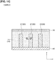
- Figure 10 is a cross-sectional view of the photovoltaic device according to another embodiment of the invention. This embodiment is different from the first embodiment in the length of the intervals between the plurality of the dissociation regions 21.
- the other configurations are the same as the above-described first embodiment, and the descriptions thereof are incorporated by reference.
- the dissociation region 21a faces the dissociation region 21b across the organic semiconductor 10 in the x direction, as is illustrated in Figure 10 .
- An opposing surface 21A and an opposing surface 21B are arranged such that the surfaces thereof face each other across a distance D.
- the opposing surface 21A is the surface of the dissociation region 21a that faces the dissociation region 21b.
- the opposing surface 21B is the surface of the dissociation region 21b that faces the dissociation region 21a.
- the opposing surfaces 21A, 21B are surfaces along the direction of extension (y direction) of the dissociation regions 21a, 21b.
- the distance D is within twice the diffusion length of the excitons.
- the diffusion length of the organic semiconductor is from several nm to about 20 nm in many materials.
- the excitons generated in the organic semiconductor 10 diffuse to the left and right with a length equivalent to the diffusion length. That is, if the donor-acceptor interface (p-n interface) does not exist in an interval of within twice the diffusion length, the electrons and holes of the excitons will recombine, causing energy loss.
- the dissociation regions 21a, 21b are arranged such that the distance D is within twice the diffusion length of the excitons. It is thereby possible to increase the dissociation efficiency of the excitons while suppressing the recombination of excitons.
- Figure 11 is a cross-sectional view of the photovoltaic device according to another embodiment of the invention.
- Figure 12 is an energy diagram in a cross section taken through line XII-XII of Figure 11 .
- the horizontal axis (X) in Figure 12 indicates the same position as the x axis in Figure 11
- the vertical axis (E) represents the energy magnitude.
- This embodiment differs from the first embodiment in the configuration of the photoactive region 11.
- the other configurations are the same as the above-described first embodiment, and the descriptions of the first to the third embodiments are incorporated where appropriate.
- the photoactive region 11 is formed by mixing an organic semiconductor donor (p-type) and an organic semiconductor acceptor (n-type) to form a bulk heterojunction in which the donor-acceptor interface is distributed over the entire region.
- the interface 63 is an interface between the photoactive region 11 and the dissociation regions 21.
- the interface 64 is a bulk heterojunction interface in the photoactive region 11.
- an exciton 50a reaches the interface 63 and dissociates.
- the exciton 50b that is not directed toward the interface 63 reaches the interface 64 and is thereby dissociated. It is thus possible to increase the conversion efficiency.
- the photoactive region includes the bulk heterojunction.
- the excitons that have not been directed toward the interface 63 between the photoactive region 11 and the dissociation regions 21 reach the interface 64 existing in the bulk heterojunction, whereby the excitons are dissociated.
- the conversion efficiency can be enhanced.
- Figure 13 is a cross-sectional view of the photovoltaic device according to another embodiment of the invention.
- Figure 14 is an energy diagram in a cross section taken through line XIV-XIV of Figure 13 .
- the horizontal axis (X) in Figure 14 indicates the same position as the x axis in Figure 13
- the vertical axis (E) represents energy magnitude.
- This embodiment differs from the first embodiment in the configuration of the dissociation regions 21.
- the other configurations are the same as the above-described first embodiment, and the descriptions of the first to the fourth embodiments are incorporated where appropriate.
- the dissociation regions 21 are formed from two types of materials having different lattice constants.
- the dissociation regions 21 includes a dissociation layer 21c formed from a first type of material and a dissociation layer 21d formed from a second type of material.
- the dissociation layer 21c is formed in a columnar shape.
- the dissociation layer 21d is formed so as to cover the outer periphery of the dissociation layer 21c. There may be three or more types of materials included in the dissociation regions 21.
- the combination of the material of the dissociation layer 21c and the material of the dissociation layer 21d is at least one selected from AIN/AIGaN, AlGaN/GaN, GaN/InGaN, InGaN/InN, AlAs/AlGaAs, AlGaAs/GaAs, GaAs/InGaAs, InGaAs/InAs, AlP/AlGaP, AlGaP/GaP, GaP/GaAsP, GaAsP/GaAs, AlP/AlAsP, AlAsP/AlAs, AlAs/InAlAs, InAlAs/InAs, GaAs/GaAsSb, GaAsSb/GaSb, AlSb/AlGaSb, AlGaSb/GaSb, AlSb/AlInSb, AlInSb/lnSb, MgS/MgZnS
- the dissociation regions 21 are formed from two types of materials having different lattice constants, stress-strain acts, and the electric field is generated due to the piezoelectric effect (piezoelectric field effect). As a result, it is possible to stably generate the electric field without restriction from materials selection and sunlight conditions.
- the dissociation regions 21 have a plurality of layers 21c, 21d formed from mutually different materials, and the lattice constants of the different materials are different. Since stress-strain is generated between the materials with different lattice constants, it is possible to stably generate the electric field in the dissociation regions 21.
- the plurality of the materials that form the dissociation regions 21 are selected from the combinations described above. Thus, because materials with similar compositions are used, it is possible to form a stacked structure of inorganic materials.
- the dissociation regions 21 may be formed from the same materials having different composition ratios as a modified example of the photovoltaic device according to this embodiment. That is, the combinations of the materials that form the dissociation regions 21 is at least one selected from Al x Ga 1-x N/Al y Ga 1-y N (x ⁇ y), In xG a 1-x N/In y Ga 1-y N (x ⁇ y), AlGa x As 1-x /AlGa y As 1-y (x ⁇ y), In x Ga 1-x As/In y Ga 1-y As, AlGa x P 1-x /AlGa y P 1-y (x ⁇ y), GaAS x P 1-x /GaAs y P 1-y (x ⁇ y), AlAs x P 1-x /AlAs y P 1-y (x ⁇ y), In x Al 1-x As/In y Al 1-y As (x ⁇ y), GaAs x Sb 1-x /
- Ec and Ev of the inorganic semiconductor 20 are intrinsic energy levels that are determined by the material and the crystallinity thereof. Thus, matching the energy of the inorganic semiconductor to a specific organic semiconductor material is difficult since it entails changing the material of the inorganic semiconductor.
- Ec and Ev can be adjusted by changing the compositions during crystal growth of the semiconductor. For example, Ec and Ev can be controlled by adjusting the Al/Ga composition ratio in AIGaN and the In/Ga composition ratio in InGaN.
- multi-element compound semiconductors in which the band gap can be adjusted such as Al-In-Ga-N semiconductors and Al-In-Ga-As semiconductors often have piezoelectric properties.
- piezoelectric effect piezoelectric field effect
- Figure 15 is an energy diagram of the photovoltaic device according to another embodiment of the invention.
- Figure 15 is an energy diagram in a cross section taken through line XIV-XIV of Figure 13 .
- the horizontal axis (X) in Figure 15 indicates the same position as the x axis in Figure 13 and the vertical axis (E) represents the energy magnitude.
- This embodiment differs from the fifth embodiment described above in the relationship of the energy levels in the dissociation regions 21.
- the other configurations are the same as the above-described fifth embodiment, and the descriptions of the first to the fifth embodiments are incorporated where appropriate.
- the dissociation regions 21 include a plurality of the dissociation layers 21c, 21d.
- the relationship of the energy levels between the dissociation layer 21c and the dissociation layer 21d at the interface 65 satisfies the following equation (13): [Equation 13] E C 3 ⁇ E F 3 where, E C3 represents the energy level of the lower end of the conduction band of the dissociation layer 21c, and E F3 represents the Fermi level of the dissociation layer 21c.
- the stress-strain increases in the dissociation regions 21 due to an increase in the lattice mismatch ratio, and the piezoelectric field increases.
- the piezoelectric field increases and the energy level E C3 at the lower end of the conduction band becomes lower than the Fermi level E F3 , a two-dimensional electron gas is formed at the interface 65 (the darkened portion in Figure 15 ).
- the conductivity can be ensured without carrying out impurity doping or the like, the scattering of carriers by impurities can be suppressed and carrier mobility improved. Therefore, by satisfying the equation (13) above, the diffusion length can be increased.
- the dissociation regions 21 have a plurality of layers 21c, 21d formed from different materials, and the energy level of one of the plurality of layers 21c, 21d satisfies the equation (13).
- the carriers are extracted via the two-dimensional electron gas with high mobility, it is possible to increase the diffusion length.
- the dissociation regions 21 may be connected to the anode electrode 30 instead of the cathode electrode 40, and at the interface 65 between the dissociation layer 21c and the dissociation layer 21d, the relationship of the energy levels may satisfy the following equation (14): [Equation 14] E V 3 > E F 3 where E V3 represents the energy level of the upper end of the valence band of the dissociation layer 21c.
- the carriers are extracted via the two-dimensional hole gas with high mobility, it is possible to increase the diffusion length. In addition, it is possible to efficiently extract the carriers and to increase the thickness of the photoactive region 11.
- Figure 16 is an energy diagram of the photovoltaic device according to another embodiment of the invention.
- Figure 17 is an energy diagram in a cross section taken through line XVII-XVII of Figure 16 .
- the horizontal axis (X) in Figure 17 indicates the same position as the x axis in Figure 16
- the vertical axis (E) represents the energy magnitude.
- This embodiment differs from the fifth embodiment described above in the relationship of the energy levels in the dissociation regions 21.
- the other configurations are the same as the above-described first embodiment, and the descriptions of the first to the sixth embodiments are incorporated where appropriate.
- the energy level at the lower end of the conduction band between the interface 66 and the connection surface 71 decreases monotonically from the interface 66 toward the connection surface 71.
- the inclination of the energy level at the lower end of the conduction band in the dissociation regions is a gradual inclination, as illustrated in Figure 17 .
- the material of the semiconductor When a multi-element mixed-crystal material, such as AIGaN, InGaN, AIGaAs, InGaAs, GaAsP, and InGaAs, is used as the material of the semiconductor, it is possible to adjust the size of the band gap of the semiconductor by changing the composition ratio.
- the composition ratio can be adjusted by adjusting a growth parameters during crystal growth, such as temperature, pressure, and source gas ratio.
- the energy of the lower end Ec of the conduction band with respect to the position can be continuously decreased by continuously adjusting the composition ratio of the crystal.
- the inclination of Ec is the electric field strength, and the electrons 51 can obtain a thrust force oriented toward the cathode electrode 40 by the electrons 51 receiving the force of the electric field. Therefore, it is possible to extend the diffusion length.
- the potential decrease amount due to the inclination of the energy level can be suppressed to 0.3 eV or less by means of the energy level condition satisfying equation (16). As a result, it is possible to minimize the voltage loss while preventing the reverse flow of carriers.
- the energy level at the interface 66 and the energy level at the connection surface 71 satisfy the equation (16). It is thereby possible to suppress the voltage loss while preventing the reverse flow of the carriers.
- the energy level at the lower end of the conduction band between the interface 66 and the connection surface 71 decreases monotonically from the 66 interface toward the connection surface 71. It is thereby possible for the carriers to obtain a thrust force oriented toward the desired electrode by generating the electric field in the dissociation regions 21. As a result, it is possible to extend the diffusion length.
- the dissociation regions 21 may be connected to the anode electrode 30 instead of the cathode electrode 40, and the energy level at the interface 66 and the energy level at the connection surface 71 may satisfy the following equations (17) and (18) instead of equations (15) and (16): [Equation 17] E HOMO ⁇ E Va [Equation 18] E Vb ⁇ E Va ⁇ 0.3 eV
- connection surface 71 is the connection surface between the anode electrode and the dissociation regions 21 connected to the anode electrode 30. It is thereby possible for the carriers to obtain a thrust force oriented toward the desired electrode by generating the electric field in the dissociation regions 21. As a result, it is possible to extend the diffusion length.
- Figure 18 is a cross-sectional view of the photovoltaic device according to another embodiment of the invention.
- the photovoltaic device according to this embodiment is configured as a tandem type.
- the other configurations are the same as the above-described first embodiment, and the descriptions of the first to the seventh embodiments are incorporated where appropriate.
- the photovoltaic device is configured as a triple-junction tandem cell.
- the photovoltaic device comprises a top cell 100, a middle cell 200, a bottom cell 300, and tunnel recombination layers 400.
- the top cell 100 includes the organic semiconductor 10, the inorganic semiconductors 20, the anode electrode 30, and the cathode electrode 40.
- the organic semiconductor 10 included in the top cell 100 has a photoactive region 11 e.
- the inorganic semiconductors 20 included in the top cell 100 has dissociation regions 21e.
- the middle cell 200 includes the organic semiconductor 10, the inorganic semiconductors 20, the anode electrode 30, and the cathode electrode 40.
- the organic semiconductor 10 included in the middle cell 200 has a photoactive region 11f.
- the inorganic semiconductors 20 included in the middle cell 200 has dissociation regions 21f.
- the bottom cell 300 includes the organic semiconductor 10, the inorganic semiconductors 20, the anode electrode 30, and the cathode electrode 40.
- the organic semiconductor 10 included in the bottom cell 300 has a photoactive region 11g.
- the inorganic semiconductors 20 included in the bottom cell 300 has dissociation regions 21g.
- the top cell 100, the middle cell 200, and the bottom cell 300 are stacked in a normal direction (y direction in Figure 18 ) of the electrode surfaces of the anode electrode 30 and the cathode electrode 40. Since the configuration of each of the top cell 100, the middle cell 200, and the bottom cell 300 is the same as that of the semiconductor device according to the first embodiment, the descriptions thereof are omitted.
- the tunnel recombination layer 400 couples the cathode electrode 40 included in the top cell 100 and the anode electrode 30 included in the middle cell 200, and couples the cathode electrode 40 included in the middle cell 200 and the anode electrode 30 included in the bottom cell 300.
- the direction of light incidence is the direction from the anode electrode 30 of the top cell 100 toward the cathode electrode of the bottom cell 300 (negative direction of the y axis).
- the photoactive region 11 e, the photoactive region 11f, and the photoactive region 11g each have different band gaps, which become smaller along the stacking direction of the cells, from the light-incident surface. That is, among the respective band gaps of the photoactive region 11e, the photoactive region 11f, and the photoactive region 11g, the band gap on the light-incident side is greatest and sequentially decreases in the transmission direction of the band gap light.
- tandem solar cells The basic concept of tandem solar cells is utilization of the fact that the semiconductor absorbs light higher in energy than the band gap and transmits light lower in energy than the band gap.
- the energy that the carriers, which are generated by the semiconductor, etc. absorbing light, receive from the photons is greater than the band gap, the energy of the photons hv-Eg (h: Planck's constant, v: wave number of photons, Eg: band gap) is lost due to relaxation of the carriers.
- hv-Eg Planck's constant, v: wave number of photons, Eg: band gap
- this embodiment is provided with a stacked body in which a plurality of cells 100, 200, 300 are stacked, and the band gap of each of the photoactive regions 11 e, 11f, 11g included in the plurality of stacked cells 100, 200, 300 becomes smaller from the incident-light surface along the stacking direction of the cells.
- the band gap of each of the photoactive regions 11 e, 11f, 11g included in the plurality of stacked cells 100, 200, 300 becomes smaller from the incident-light surface along the stacking direction of the cells.
- the band gap on the light-incident side is greatest and sequentially decreases in the transmission direction of the band gap light proceeds in the transmission direction .
- the dissociation regions 21e, the dissociation regions 21f, and the dissociation regions 21g have the function of the photoactive region. That is, among the respective band gaps of the dissociation regions 21e, the dissociation regions 21f, and the dissociation regions 21g, the band gap on the light-incident side is the greatest and sequentially decreases in the transmission direction of the band gap light.
- Figure 19 is a cross-sectional view of the photovoltaic device according to another embodiment of the invention.
- the photovoltaic device according to this embodiment is different in the configuration of a part of the inorganic semiconductor 20.
- the other configurations are the same as the above-described first embodiment, and the descriptions of the first to the eighth embodiments are incorporated where appropriate.
- the direction of light incidence is the direction from the anode electrode 30 toward the cathode electrode 40 (negative y-axis direction).
- the inorganic semiconductor 20 is formed to cover the surface of the cathode electrode 40. Portions of the inorganic semiconductor 20 have a columnar shape, and the columnar portions are covered with the organic material of the organic semiconductor 10. Since the cathode electrode 40 is covered with the inorganic semiconductor 20, the organic semiconductor 11 and the cathode electrode 40 are not in direct contact with each other. That is, the film-like inorganic semiconductor 20 is provided between the cathode electrode and the end of the organic semiconductor 11.
- the inorganic semiconductor 20 is formed by crystal growth, such as CVD. Crystals of an inorganic material are grown on the surface of the plate-like cathode electrode 40 and growth is temporarily suspended when a film of the inorganic material is formed on the surface of the cathode electrode 40.
- a mask pattern such as a photolithography mask, is placed on the inorganic material film. Columnar crystals of the same inorganic material are grown at the openings of the mask pattern. The inorganic semiconductor 20 is thereby formed, as illustrated in Figure 19 .
- the method for producing the inorganic semiconductor 20 is not limited to crystal growth, such as CVD, and the S-K growth (Stranski-Krastanov) mode may be used instead.
- S-K growth mode When the S-K growth mode is used, of the inorganic material film that is formed on the surface of the cathode electrode 40, only a portion of the surface of the inorganic material film need be grown in columnar form.
- piezoelectric material may be grown to the height of the columnar portions shown in Figure 19 (height in the y direction), and the portions other than the columnar portions (recessed region) may be formed by etching.
- the dissociation regions 21 are surrounded by the organic material of the organic semiconductor 10, and a part of the dissociation regions 21 are directly connected to the cathode electrode 40, while the cathode electrode and the photoactive region 11 are not in direct contact.
- a localized energy level is formed at the interface between the organic semiconductor 10 and the cathode 40, depending on the combination of the organic material of the organic semiconductor 10 and the material of the cathode electrode 40. If the localized energy level is a level that promotes carrier recombination, a dipole (electric dipole) is formed at the interface, thereby making it difficult to obtain the desired characteristics.
- the organic semiconductor 10 and the cathode electrode 40 are not in direct contact, a localized energy level that promotes carrier recombination is not generated, and formation of the dipole at the interface can be prevented.
- the photovoltaic device according to this embodiment may have the structure shown in Figure 20 as a structure in which the organic semiconductor 10 and the cathode electrode 40 are not in direct contact with each other.
- FIG 20 is a cross-sectional view of the photovoltaic device according to a modified example of this embodiment.
- the photovoltaic device according to the present modified example comprises the organic semiconductor 10, the inorganic semiconductor 20, the anode electrode 30, the cathode electrode 40, and a protective film 70.
- the protective film 70 is provided between the organic semiconductor 10 and the cathode electrode 40.
- the protective film 70 is formed on the surface of the cathode electrode 40 so as to cover the portion of the surface of the cathode electrode 40 that is not connected to the dissociation regions 21.
- the protective layer 70 may have an insulating property.
- the protective layer 70 is formed of an oxide film obtained by oxidizing a metal surface or by means of a growth method (CVD, etc.). After forming the protective layer on the surface of the cathode electrode 40, the portion where the dissociation regions 21 are to be formed are opened by means of photolithography. The dissociation regions 21 are formed by crystal growth of the inorganic material at the opened portions
- the photovoltaic device according to this embodiment may have the structure shown in Figure 21 as a structure in which the organic semiconductor 10 and the cathode electrode 40 are not in direct contact with each other.
- Figure 21 is a cross-sectional view of the photovoltaic device according to a modified example of this embodiment.
- the inorganic semiconductors 20 are formed in a columnar shape extending in the y-axis direction, while covering the surface of the cathode electrode 40 with a layer.
- the columnar portions are covered with the organic material of the organic semiconductor 10.
- the protective film 70 is provided between the organic semiconductor 10 and the inorganic semiconductor 20.
- the protective film 70 is formed so as to cover the layer portion of the inorganic semiconductor 20.
- the protective film 70 prevents the cathode electrode 40 and the organic semiconductor 10 from coming into direct contact with each other.
Applications Claiming Priority (1)
| Application Number | Priority Date | Filing Date | Title |
|---|---|---|---|
| PCT/JP2016/075579 WO2018042579A1 (ja) | 2016-08-31 | 2016-08-31 | 光起電力装置 |
Publications (2)
| Publication Number | Publication Date |
|---|---|
| EP3509115A1 true EP3509115A1 (de) | 2019-07-10 |
| EP3509115A4 EP3509115A4 (de) | 2019-09-18 |
Family
ID=61300394
Family Applications (1)
| Application Number | Title | Priority Date | Filing Date |
|---|---|---|---|
| EP16915140.4A Pending EP3509115A4 (de) | 2016-08-31 | 2016-08-31 | Pv-element |
Country Status (5)
| Country | Link |
|---|---|
| US (1) | US11183655B2 (de) |
| EP (1) | EP3509115A4 (de) |
| JP (1) | JP6791249B2 (de) |
| CN (1) | CN109690800B (de) |
| WO (1) | WO2018042579A1 (de) |
Families Citing this family (3)
| Publication number | Priority date | Publication date | Assignee | Title |
|---|---|---|---|---|
| CN113130761B (zh) * | 2021-03-19 | 2022-04-19 | 太原理工大学 | 双向偏压响应的有机光电倍增探测器及其制备方法 |
| CN113816909B (zh) * | 2021-09-15 | 2023-07-11 | 武汉尚赛光电科技有限公司 | 一种含菲结构的有机电致发光材料及其器件 |
| CN115504678B (zh) * | 2022-11-03 | 2023-09-29 | 业泓科技(成都)有限公司 | 触控识别模组的减薄方法 |
Family Cites Families (16)
| Publication number | Priority date | Publication date | Assignee | Title |
|---|---|---|---|---|
| JP3423280B2 (ja) * | 2000-09-25 | 2003-07-07 | 科学技術振興事業団 | 有機・無機複合薄膜太陽電池 |
| KR101008294B1 (ko) | 2001-03-30 | 2011-01-13 | 더 리전트 오브 더 유니버시티 오브 캘리포니아 | 나노구조체 및 나노와이어의 제조 방법 및 그로부터 제조되는 디바이스 |
| US6878871B2 (en) * | 2002-09-05 | 2005-04-12 | Nanosys, Inc. | Nanostructure and nanocomposite based compositions and photovoltaic devices |
| JP4514402B2 (ja) | 2002-10-28 | 2010-07-28 | シャープ株式会社 | 半導体素子及びその製造方法 |
| US6969897B2 (en) | 2002-12-10 | 2005-11-29 | Kim Ii John | Optoelectronic devices employing fibers for light collection and emission |
| CN101336489B (zh) * | 2005-12-02 | 2012-07-18 | 海利安特斯有限公司 | 光伏电池 |
| US8987589B2 (en) * | 2006-07-14 | 2015-03-24 | The Regents Of The University Of Michigan | Architectures and criteria for the design of high efficiency organic photovoltaic cells |
| US7705523B2 (en) * | 2008-05-27 | 2010-04-27 | Georgia Tech Research Corporation | Hybrid solar nanogenerator cells |
| EP2172986B1 (de) * | 2008-08-27 | 2013-08-21 | Honeywell International Inc. | Solarzelle mit Hybrid-Hetero-Verbindungsstruktur |
| WO2010117330A1 (en) * | 2009-04-09 | 2010-10-14 | Fredrik Boxberg | Photovoltaic device, and a manufacturing method thereof |
| KR20100130514A (ko) * | 2009-06-03 | 2010-12-13 | 삼성전자주식회사 | 유기 태양 전지 및 그 제조방법 |
| EP2290718B1 (de) * | 2009-08-25 | 2015-05-27 | Samsung Electronics Co., Ltd. | Vorrichtung zur Erzeugung elektrischer Energie und Herstellungsverfahren dafür |
| JP2011135058A (ja) * | 2009-11-30 | 2011-07-07 | Honda Motor Co Ltd | 太陽電池素子、カラーセンサ、ならびに発光素子及び受光素子の製造方法 |
| JP5568039B2 (ja) * | 2011-03-15 | 2014-08-06 | 国立大学法人 東京大学 | 太陽電池 |
| FR2973945B1 (fr) * | 2011-04-11 | 2013-05-10 | Centre Nat Rech Scient | Heterostructure semi-conductrice et cellule photovoltaïque comprenant une telle heterostructure |
| JP2014179537A (ja) * | 2013-03-15 | 2014-09-25 | Sumitomo Chemical Co Ltd | 無機・有機ハイブリッド光電変換素子 |
-
2016
- 2016-08-31 JP JP2018536603A patent/JP6791249B2/ja active Active
- 2016-08-31 WO PCT/JP2016/075579 patent/WO2018042579A1/ja unknown
- 2016-08-31 EP EP16915140.4A patent/EP3509115A4/de active Pending
- 2016-08-31 US US16/325,041 patent/US11183655B2/en active Active
- 2016-08-31 CN CN201680088889.0A patent/CN109690800B/zh active Active
Also Published As
| Publication number | Publication date |
|---|---|
| JP6791249B2 (ja) | 2020-11-25 |
| US20210305524A1 (en) | 2021-09-30 |
| US11183655B2 (en) | 2021-11-23 |
| EP3509115A4 (de) | 2019-09-18 |
| WO2018042579A1 (ja) | 2018-03-08 |
| CN109690800A (zh) | 2019-04-26 |
| CN109690800B (zh) | 2023-01-06 |
| JPWO2018042579A1 (ja) | 2019-08-08 |
Similar Documents
| Publication | Publication Date | Title |
|---|---|---|
| US10290755B1 (en) | High efficiency photovoltaic cells and manufacturing thereof | |
| US9905714B2 (en) | High efficiency photovoltaic cells | |
| TWI441346B (zh) | 第ⅱ型量子點太陽能電池 | |
| US8624107B2 (en) | Photovoltaic cells based on nanoscale structures | |
| US8716594B2 (en) | High efficiency photovoltaic cells with self concentrating effect | |
| US20100180936A1 (en) | Multijunction solar cell | |
| US20070204901A1 (en) | Photovoltaic cells based on nano or micro-scale structures | |
| JP2009527108A (ja) | ナノ構造層を備える光起電装置 | |
| KR20130133156A (ko) | 등급화된 재결합 층에 의해 분리된 다중 접합부들을 갖는 광전지 디바이스들 | |
| CN102144304A (zh) | 具有高转换效率的光伏电池 | |
| EP2837038A2 (de) | Fotovoltaiknanoverbundstoff mit lösungsverarbeiteten anorganischen bulk-nano-heteroübergängen, solarzelle und fotodiodenvorrichtungen mit dem nanoverbundstoff | |
| US20150162469A1 (en) | Dilute group iii-v nitride intermediate band solar cells with contact blocking layers | |
| US11183655B2 (en) | Photovoltaic device | |
| US9006931B2 (en) | Static-electrical-field-enhanced semiconductor-based devices and methods of enhancing semiconductor-based device performance | |
| WO2012166993A1 (en) | Charge-coupled photovoltaic devices | |
| CN103688366B (zh) | 半导体异质结构和包括该异质结构的光伏电池 | |
| Chien et al. | Formation of Ge quantum dots array in layer-cake technique for advanced photovoltaics | |
| Ojo et al. | Photovoltaic Solar Cells: Materials, Concepts and Devices | |
| WO2010018490A2 (en) | A photovoltaic cell and a method of manufacturing the same | |
| WO2013055429A2 (en) | Quantum dot structures for efficient photovoltaic conversion, and methods of using and making the same | |
| Kechiantz et al. | Efficiency limit of intermediate band AlxGa1-xAs solar cell based on AlyGa1-ySb type-II quantum dots embedded outside of the depletion region | |
| Barletta et al. | Si/Ge nanodot superlattices for Si-based photovoltaics |
Legal Events
| Date | Code | Title | Description |
|---|---|---|---|
| STAA | Information on the status of an ep patent application or granted ep patent |
Free format text: STATUS: THE INTERNATIONAL PUBLICATION HAS BEEN MADE |
|
| PUAI | Public reference made under article 153(3) epc to a published international application that has entered the european phase |
Free format text: ORIGINAL CODE: 0009012 |
|
| STAA | Information on the status of an ep patent application or granted ep patent |
Free format text: STATUS: REQUEST FOR EXAMINATION WAS MADE |
|
| 17P | Request for examination filed |
Effective date: 20190320 |
|
| AK | Designated contracting states |
Kind code of ref document: A1 Designated state(s): AL AT BE BG CH CY CZ DE DK EE ES FI FR GB GR HR HU IE IS IT LI LT LU LV MC MK MT NL NO PL PT RO RS SE SI SK SM TR |
|
| AX | Request for extension of the european patent |
Extension state: BA ME |
|
| A4 | Supplementary search report drawn up and despatched |
Effective date: 20190816 |
|
| RIC1 | Information provided on ipc code assigned before grant |
Ipc: H01L 51/44 20060101AFI20190809BHEP Ipc: H01L 51/42 20060101ALI20190809BHEP Ipc: H01L 41/113 20060101ALI20190809BHEP |
|
| DAV | Request for validation of the european patent (deleted) | ||
| DAX | Request for extension of the european patent (deleted) | ||
| STAA | Information on the status of an ep patent application or granted ep patent |
Free format text: STATUS: EXAMINATION IS IN PROGRESS |
|
| STAA | Information on the status of an ep patent application or granted ep patent |
Free format text: STATUS: EXAMINATION IS IN PROGRESS |
|
| 17Q | First examination report despatched |
Effective date: 20211203 |
|
| REG | Reference to a national code |
Ref country code: DE Ref legal event code: R079 Free format text: PREVIOUS MAIN CLASS: H01L0051440000 Ipc: H10K0030100000 |
|
| GRAP | Despatch of communication of intention to grant a patent |
Free format text: ORIGINAL CODE: EPIDOSNIGR1 |
|
| STAA | Information on the status of an ep patent application or granted ep patent |
Free format text: STATUS: GRANT OF PATENT IS INTENDED |
|
| RIC1 | Information provided on ipc code assigned before grant |
Ipc: H10N 30/30 20230101ALI20240319BHEP Ipc: H10K 30/35 20230101ALI20240319BHEP Ipc: H10K 30/10 20230101AFI20240319BHEP |
|
| INTG | Intention to grant announced |
Effective date: 20240404 |