EP3507630B1 - Verfahren und system zur optischen ausrichtung mit einer photonisch aktivierten integrierten siliciumschaltung - Google Patents
Verfahren und system zur optischen ausrichtung mit einer photonisch aktivierten integrierten siliciumschaltung Download PDFInfo
- Publication number
- EP3507630B1 EP3507630B1 EP17765049.6A EP17765049A EP3507630B1 EP 3507630 B1 EP3507630 B1 EP 3507630B1 EP 17765049 A EP17765049 A EP 17765049A EP 3507630 B1 EP3507630 B1 EP 3507630B1
- Authority
- EP
- European Patent Office
- Prior art keywords
- optical
- grating couplers
- output
- fiber
- assembly
- Prior art date
- Legal status (The legal status is an assumption and is not a legal conclusion. Google has not performed a legal analysis and makes no representation as to the accuracy of the status listed.)
- Active
Links
Images


Classifications
-
- H—ELECTRICITY
- H04—ELECTRIC COMMUNICATION TECHNIQUE
- H04B—TRANSMISSION
- H04B10/00—Transmission systems employing electromagnetic waves other than radio-waves, e.g. infrared, visible or ultraviolet light, or employing corpuscular radiation, e.g. quantum communication
- H04B10/40—Transceivers
-
- G—PHYSICS
- G02—OPTICS
- G02B—OPTICAL ELEMENTS, SYSTEMS OR APPARATUS
- G02B6/00—Light guides; Structural details of arrangements comprising light guides and other optical elements, e.g. couplings
- G02B6/02—Optical fibres with cladding with or without a coating
- G02B6/028—Optical fibres with cladding with or without a coating with core or cladding having graded refractive index
- G02B6/0288—Multimode fibre, e.g. graded index core for compensating modal dispersion
-
- G—PHYSICS
- G02—OPTICS
- G02B—OPTICAL ELEMENTS, SYSTEMS OR APPARATUS
- G02B6/00—Light guides; Structural details of arrangements comprising light guides and other optical elements, e.g. couplings
- G02B6/10—Light guides; Structural details of arrangements comprising light guides and other optical elements, e.g. couplings of the optical waveguide type
- G02B6/12—Light guides; Structural details of arrangements comprising light guides and other optical elements, e.g. couplings of the optical waveguide type of the integrated circuit kind
- G02B6/122—Basic optical elements, e.g. light-guiding paths
- G02B6/124—Geodesic lenses or integrated gratings
-
- G—PHYSICS
- G02—OPTICS
- G02B—OPTICAL ELEMENTS, SYSTEMS OR APPARATUS
- G02B6/00—Light guides; Structural details of arrangements comprising light guides and other optical elements, e.g. couplings
- G02B6/24—Coupling light guides
- G02B6/42—Coupling light guides with opto-electronic elements
- G02B6/4201—Packages, e.g. shape, construction, internal or external details
- G02B6/4204—Packages, e.g. shape, construction, internal or external details the coupling comprising intermediate optical elements, e.g. lenses, holograms
- G02B6/4213—Packages, e.g. shape, construction, internal or external details the coupling comprising intermediate optical elements, e.g. lenses, holograms the intermediate optical elements being polarisation selective optical elements
-
- G—PHYSICS
- G02—OPTICS
- G02B—OPTICAL ELEMENTS, SYSTEMS OR APPARATUS
- G02B6/00—Light guides; Structural details of arrangements comprising light guides and other optical elements, e.g. couplings
- G02B6/24—Coupling light guides
- G02B6/42—Coupling light guides with opto-electronic elements
- G02B6/4201—Packages, e.g. shape, construction, internal or external details
- G02B6/4204—Packages, e.g. shape, construction, internal or external details the coupling comprising intermediate optical elements, e.g. lenses, holograms
- G02B6/4214—Packages, e.g. shape, construction, internal or external details the coupling comprising intermediate optical elements, e.g. lenses, holograms the intermediate optical element having redirecting reflective means, e.g. mirrors, prisms for deflecting the radiation from horizontal to down- or upward direction toward a device
-
- G—PHYSICS
- G02—OPTICS
- G02B—OPTICAL ELEMENTS, SYSTEMS OR APPARATUS
- G02B6/00—Light guides; Structural details of arrangements comprising light guides and other optical elements, e.g. couplings
- G02B6/24—Coupling light guides
- G02B6/42—Coupling light guides with opto-electronic elements
- G02B6/4201—Packages, e.g. shape, construction, internal or external details
- G02B6/4219—Mechanical fixtures for holding or positioning the elements relative to each other in the couplings; Alignment methods for the elements, e.g. measuring or observing methods especially used therefor
- G02B6/422—Active alignment, i.e. moving the elements in response to the detected degree of coupling or position of the elements
-
- G—PHYSICS
- G02—OPTICS
- G02B—OPTICAL ELEMENTS, SYSTEMS OR APPARATUS
- G02B6/00—Light guides; Structural details of arrangements comprising light guides and other optical elements, e.g. couplings
- G02B6/24—Coupling light guides
- G02B6/42—Coupling light guides with opto-electronic elements
- G02B6/4201—Packages, e.g. shape, construction, internal or external details
- G02B6/4246—Bidirectionally operating package structures
-
- G—PHYSICS
- G02—OPTICS
- G02B—OPTICAL ELEMENTS, SYSTEMS OR APPARATUS
- G02B6/00—Light guides; Structural details of arrangements comprising light guides and other optical elements, e.g. couplings
- G02B6/24—Coupling light guides
- G02B6/42—Coupling light guides with opto-electronic elements
- G02B6/4201—Packages, e.g. shape, construction, internal or external details
- G02B6/4256—Details of housings
- G02B6/426—Details of housings mounting, engaging or coupling of the package to a board, a frame or a panel
-
- G—PHYSICS
- G02—OPTICS
- G02B—OPTICAL ELEMENTS, SYSTEMS OR APPARATUS
- G02B6/00—Light guides; Structural details of arrangements comprising light guides and other optical elements, e.g. couplings
- G02B6/24—Coupling light guides
- G02B6/42—Coupling light guides with opto-electronic elements
- G02B6/4295—Coupling light guides with opto-electronic elements coupling with semiconductor devices activated by light through the light guide, e.g. thyristors, phototransistors
-
- H—ELECTRICITY
- H04—ELECTRIC COMMUNICATION TECHNIQUE
- H04B—TRANSMISSION
- H04B10/00—Transmission systems employing electromagnetic waves other than radio-waves, e.g. infrared, visible or ultraviolet light, or employing corpuscular radiation, e.g. quantum communication
- H04B10/25—Arrangements specific to fibre transmission
- H04B10/2581—Multimode transmission
-
- H—ELECTRICITY
- H05—ELECTRIC TECHNIQUES NOT OTHERWISE PROVIDED FOR
- H05K—PRINTED CIRCUITS; CASINGS OR CONSTRUCTIONAL DETAILS OF ELECTRIC APPARATUS; MANUFACTURE OF ASSEMBLAGES OF ELECTRICAL COMPONENTS
- H05K13/00—Apparatus or processes specially adapted for manufacturing or adjusting assemblages of electric components
- H05K13/04—Mounting of components, e.g. of leadless components
- H05K13/0404—Pick-and-place heads or apparatus, e.g. with jaws
-
- H—ELECTRICITY
- H10—SEMICONDUCTOR DEVICES; ELECTRIC SOLID-STATE DEVICES NOT OTHERWISE PROVIDED FOR
- H10P—GENERIC PROCESSES OR APPARATUS FOR THE MANUFACTURE OR TREATMENT OF DEVICES COVERED BY CLASS H10
- H10P72/00—Handling or holding of wafers, substrates or devices during manufacture or treatment thereof
- H10P72/50—Handling or holding of wafers, substrates or devices during manufacture or treatment thereof for positioning, orientation or alignment
- H10P72/53—Handling or holding of wafers, substrates or devices during manufacture or treatment thereof for positioning, orientation or alignment using optical controlling means
-
- G—PHYSICS
- G02—OPTICS
- G02B—OPTICAL ELEMENTS, SYSTEMS OR APPARATUS
- G02B6/00—Light guides; Structural details of arrangements comprising light guides and other optical elements, e.g. couplings
- G02B6/10—Light guides; Structural details of arrangements comprising light guides and other optical elements, e.g. couplings of the optical waveguide type
- G02B6/12—Light guides; Structural details of arrangements comprising light guides and other optical elements, e.g. couplings of the optical waveguide type of the integrated circuit kind
- G02B2006/12133—Functions
- G02B2006/12147—Coupler
Definitions
- aspects of the present disclosure relate to electronic components. More specifically, certain implementations of the present disclosure relate to methods and systems for optical alignment to a silicon photonically-enabled integrated circuit.
- a photonic integrated circuit may be optically aligned to a plurality of optical components (e.g., an optical fiber array).
- Optical alignment may be facilitated by the use of an optical impedance element coupled between a first input/output (I/O) optical waveguide and a second I/O optical waveguide of the PIC.
- the optical impedance element me be configured to be transmissive during optical alignment and to be non-transmissive during the regular operation of the PIC.
- a wafer test system includes an input device configured to transmit a test signal, a wafer including an optical port, an input port configured to receive the test signal, and an output port configured to output a result signal based on the test signal, a measuring device configured to measure the result signal, and an alignment device configured to align an optical fiber port of an optical probe with an alignment port based on the result signal and then align the optical fiber port with the optical port.
- the alignment port is the input port or the output port.
- the optical probe is configured to be the input device when the input port is the alignment port and the optical probe is configured to be the measuring device when the output port is the alignment port.
- circuits and circuitry refer to physical electronic components (i.e. hardware) and any software and/or firmware ("code") which may configure the hardware, be executed by the hardware, and or otherwise be associated with the hardware.
- code software and/or firmware
- a particular processor and memory may comprise a first "circuit” when executing a first one or more lines of code and may comprise a second "circuit” when executing a second one or more lines of code.
- and/or means any one or more of the items in the list joined by “and/or”.
- x and/or y means any element of the three-element set ⁇ (x), (y), (x, y) ⁇ .
- x and/or y means “one or both of x and y”.
- x, y, and/or z means any element of the seven-element set ⁇ (x), (y), (z), (x, y), (x, z), (y, z), (x, y, z) ⁇ .
- x, y and/or z means “one or more of x, y and z”.
- exemplary means serving as a non-limiting example, instance, or illustration.
- the terms "e.g.,” and “for example” set off lists of one or more non-limiting examples, instances, or illustrations.
- circuitry or a device is "operable" to perform a function whenever the circuitry or device comprises the necessary hardware and code (if any is necessary) to perform the function, regardless of whether performance of the function is disabled or not enabled (e.g., by a user-configurable setting, factory trim, etc.).
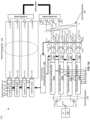
- FIG. 1A is a block diagram of a photonically-enabled integrated circuit with built-in optical alignment, in accordance with an example embodiment of the disclosure.
- optoelectronic devices on a photonically-enabled integrated circuit 130 comprising optical modulators 105A-105D, photodiodes 111A-111D, monitor photodiodes 113A-113H, and optical devices comprising couplers 103A-103K, optical terminations 115A-115D, and grating couplers 117A-117H.
- electrical devices and circuits comprising amplifiers 107A-107D, analog and digital control circuits 109, and control sections 112A-112D.
- the amplifiers 107A-107D may comprise transimpedance and limiting amplifiers (TIA/LAs), for example.
- the photonically-enabled integrated circuit 130 comprises a CMOS photonics die with a laser assembly 101 coupled to the top surface of the IC 130.
- the laser assembly 101 may comprise one or more semiconductor lasers with isolators, lenses, and/or rotators for directing one or more CW optical signals to the coupler 103A.
- the photonically enabled integrated circuit 130 may comprise a single chip, or may be integrated on a plurality of die, such as one or more electronics die and one or more photonics die.
- Optical signals are communicated between optical and optoelectronic devices via optical waveguides 110 fabricated in the photonically-enabled integrated circuit 130.
- Single-mode or multi-mode waveguides may be used in photonic integrated circuits. Single-mode operation enables direct connection to optical signal processing and networking elements.
- the term "single-mode" may be used for waveguides that support a single mode for each of the two polarizations, transverse-electric (TE) and transverse-magnetic (TM), or for waveguides that are truly single mode and only support one mode whose polarization is TE, which comprises an electric field parallel to the substrate supporting the waveguides.
- Two typical waveguide cross-sections that are utilized comprise strip waveguides and rib waveguides. Strip waveguides typically comprise a rectangular cross-section, whereas rib waveguides comprise a rib section on top of a waveguide slab. Of course, other waveguide cross section types are also contemplated and within the scope of the disclosure.
- the couplers 103A-103C may comprise low-loss Y-junction power splitters where coupler 103A receives an optical signal from the laser assembly 101 and splits the signal to two branches that direct the optical signals to the couplers 103B and 103C, which split the optical signal once more, resulting in four roughly equal power optical signals.
- the optical power splitter may comprise at least one input waveguide and at least two output waveguides.
- the couplers 103A-103C shown in FIG. 1A illustrates 1-by-2 splitters, which divide the optical power in one waveguide into two other waveguides evenly.
- These Y-junction splitters may be used in multiple locations in an optoelectronic system, such as in a Mach-Zehnder interferometer (MZI) modulator, e.g., the optical modulators 105A-105D, where a splitter and a combiner are needed, since a power combiner can be a splitter used in reverse.
- MZI Mach-Zehnder interferometer
- the Y-junction may be utilized in a parallel multichannel transmitter, where a cascade of 1-by-2 splitters can be employed to have a single light source feed multiple channels.
- Interleaver-based multiplexers and demultiplexers constitute a third example where 1-by-2 splitters are among the building blocks.
- the optical modulators 105A-105D comprise Mach-Zehnder or ring modulators, for example, and enable the modulation of the continuous-wave (CW) laser input signal.
- the optical modulators 105A-105D may comprise high-speed and low-speed phase modulation sections and are controlled by the control sections 112A-112D.
- the high-speed phase modulation section of the optical modulators 105A-105D may modulate a CW light source signal with a data signal.
- the low-speed phase modulation section of the optical modulators 105A-105D may compensate for slowly varying phase factors such as those induced by mismatch between the waveguides, waveguide temperature, or waveguide stress and is referred to as the passive phase, or the passive biasing of the MZI.
- the high-speed optical phase modulators may operate based on the free carrier dispersion effect and may demonstrate a high overlap between the free carrier modulation region and the optical mode.
- High-speed phase modulation of an optical mode propagating in a waveguide is the building block of several types of signal encoding used for high data rate optical communications.
- Speed in the several Gb/s may be required to sustain the high data rates used in modern optical links and can be achieved in integrated Si photonics by modulating the depletion region of a PN junction placed across the waveguide carrying the optical beam.
- the overlap between the optical mode and the depletion region of the PN junction is optimized.
- the outputs of the optical modulators 105A-105D may be optically coupled via the waveguides 110 to the grating couplers 117E-117H.
- the couplers 103D-103K may comprise four-port optical couplers, for example, and may be utilized to sample or split the optical signals generated by the optical modulators 105A-105D, with the sampled signals being measured by the monitor photodiodes 113A-113H.
- the unused branches of the directional couplers 103D-103K may be terminated by optical terminations 115A-115D to avoid back reflections of unwanted signals.
- the grating couplers 117A-117H comprise optical gratings that enable coupling of light into and out of the photonically-enabled integrated circuit 130.
- the grating couplers 117A-117D may be utilized to couple light received from optical fibers into the photonically-enabled integrated circuit 130, and the grating couplers 117E-117H may be utilized to couple light from the photonically-enabled integrated circuit 130 into optical fibers.
- the grating couplers 117A-117H may comprise single polarization grating couplers (SPGC) and/or polarization splitting grating couplers (PSGC). In instances where a PSGC is utilized, two input, or output, waveguides may be utilized.
- SPGC single polarization grating couplers
- PSGC polarization splitting grating couplers
- the optical fibers may be affixed using epoxy, for example, to the CMOS chip, and may be aligned at an angle from normal to the surface of the photonically-enabled integrated circuit 130 to optimize coupling efficiency.
- the optical fibers may comprise single-mode fiber (SMF) and/or polarization-maintaining fiber (PMF).
- the photodiodes 111A-111D may convert optical signals received from the grating couplers 117A-117D into electrical signals that are communicated to the amplifiers 107A-107D for processing.
- the photodiodes 111A-111D may comprise high-speed heterojunction phototransistors, for example, and may comprise germanium (Ge) in the collector and base regions for absorption in the 1.3-1.6 ⁇ m optical wavelength range, and may be integrated on a CMOS silicon-on-insulator (SOI) wafer.
- the receiver subsystem implemented in a silicon chip
- light is often coupled into a photodetector via a polarization-splitting grating coupler that supports coupling all polarization states of the fiber mode efficiently.
- the incoming signal is split by the PSGC into two separate waveguides in a polarization-diversity scheme, and therefore both inputs to the waveguide photodetectors are used. If two different PSGCs are required to couple into the same photodetector, then the PD has have four separate waveguide ports.
- the analog and digital control circuits 109 may control gain levels or other parameters in the operation of the amplifiers 107A-107D, which may then communicate electrical signals off the photonically-enabled integrated circuit 130.
- the control sections 112A-112D comprise electronic circuitry that enable modulation of the CW laser signal received from the splitters 103A-103C.
- the optical modulators 105A-105D may require high-speed electrical signals to modulate the refractive index in respective branches of a Mach-Zehnder interferometer (MZI), for example.
- MZI Mach-Zehnder interferometer
- the photonically-enabled integrated circuit 130 may be operable to transmit and/or receive and process optical signals.
- Optical signals may be received from optical fibers by the grating couplers 117A-117D and converted to electrical signals by the photodetectors 111A-111D.
- the electrical signals may be amplified by transimpedance amplifiers in the amplifiers 107A-107D, for example, and subsequently communicated to other electronic circuitry, not shown, in the photonically-enabled integrated circuit 130.
- An optical transceiver chip contains optoelectronic circuits that create and process the optical/electrical signals on the transmitter (Tx) and the receiver (Rx) sides, as well as optical interfaces that couple the optical signals to and from a fiber.
- the signal processing functionality may include modulating the optical carrier, detecting the optical signal, splitting or combining data streams, and multiplexing or demultiplexing data on carriers with different wavelengths, and equalizing signals for reducing and/or eliminating inter-symbol interference (ISI), which may be a common impairment in optical communication systems.
- ISI inter-symbol interference
- passive optical taps with feedback loops to grating couplers for transmission back out of the chip may be utilized in the photonically-enabled integrated circuit 130 to enable active alignment to the photonically enabled integrated circuits.
- the disclosure allows the construction of a passive (i.e. not requiring power or control of silicon photonically-enabled integrated circuit), product-independent, and design-rule driven platform for scalable and cost effective active optical alignment to silicon photonically-enabled integrated circuits.
- the method and system can be used for both packaging and test of components constructed from silicon photonically enabled integrated circuits.
- accurate monitoring of the alignment stability of temperature sensitive light sources through the attach process using a normalization detector is disclosed.
- Silicon photonically-enabled integrated circuit technology allows for the ubiquitous use of optical library components that can be integrated compactly, with essentially no additional cost, into large scale electro-optical circuits.
- the disclosure describes using passive optical sub-circuits connected to the photonic input/output nodes of a silicon photonic die, combined together with optically enabled tooling, to create optical feedback signal for active optical alignment of input/output components.
- the disclosed system and method do not rely on the inward or outward coupling path for any particular product, but rather follows product-independent design rules, which allows a more general solution to the technological problem of active optical alignment that is made practical by the ability to freely add passive optical components such as splitters and surface grating couplers to photonic integrated circuits.
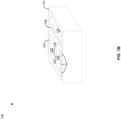
- FIG. 1B is a diagram illustrating an exemplary photonically-enabled integrated circuit, in accordance with an example embodiment of the disclosure.
- the photonically-enabled integrated circuit 130 comprising electronic devices/circuits 131, optical and optoelectronic devices 133, a light source interface 135, a chip front surface 137, an optical fiber interface 139, CMOS guard ring 141, and a surface-illuminated monitor photodiode 143.
- the light source interface 135 and the optical fiber interface 139 comprise grating couplers, for example, that enable coupling of light signals via the CMOS chip surface 137, as opposed to the edges of the chip as with conventional edge-emitting/receiving devices. Coupling light signals via the chip surface 137 enables the use of the CMOS guard ring 141 which protects the chip mechanically and prevents the entry of contaminants via the chip edge.
- the electronic devices/circuits 131 comprise circuitry such as the amplifiers 107A-107D and the analog and digital control circuits 109 described with respect to FIG. 1A , for example.
- the optical and optoelectronic devices 133 comprise devices such as the couplers 103A-103K, optical terminations 115A-115D, grating couplers 117A-117H, optical modulators 105A-105D, high-speed heterojunction photodiodes 111A-111D, and monitor photodiodes 113A-113I.
- FIG. 1C is a diagram illustrating a photonically-enabled integrated circuit coupled to an optical fiber cable, in accordance with an example embodiment of the disclosure.
- the photonically-enabled integrated circuit 130 comprising the chip surface 137 and the CMOS guard ring 141.
- the fiber-to-chip coupler 145 there are also shown a fiber-to-chip coupler 145, an optical fiber cable 149, and an optical source assembly 147.
- the photonically-enabled integrated circuit 130 comprises the electronic devices/circuits 131, the optical and optoelectronic devices 133, the light source interface 135, the chip surface 137, and the CMOS guard ring 141 may be as described with respect to FIG. 1B for example.
- the optical fiber cable may be affixed, via epoxy for example, to the CMOS chip surface 137.
- the fiber chip coupler 145 enables the physical coupling of the optical fiber cable 149 to the photonically-enabled integrated circuit 130.
- the IC 130 may comprise photonic devices on one die, such as a photonics interposer, and electrical devices on an electronics die, both of which may comprise CMOS die.
- the coupling of the fiber-to-chip coupler 145 and the optical source assembly 147 may be enabled with a gripper in a pick-and-place tool that comprises one or more optical fibers that coupled to couplers in the optical chip 135 such that the optical circuitry and/or the optical sources may be tested in an active alignment procedure, while not requiring the powering up of the chip 135.
- This "pseudo-active" alignment follows product-independent design rules, which allows a more general solution to the technological problem of active optical alignment that is made practical by the ability to freely add passive optical components such as splitters and surface grating couplers to photonic integrated circuits.
- the chip 135 may instead comprise a plurality of die.
- one or more electronic die may be coupled to a photonics die, i.e., a photonic interposer, comprising optical and optoelectronic devices for communicating optical signals between electronics die, for example.
- FIG. 2 illustrates a micro-packaged laser light source to be aligned to an photonic integrated circuit, in accordance with an example embodiment of the disclosure.
- a component 201 may comprise a micro-packaged light source that may be configured to direct an output beam through the bottom of the package at an angle that is designed to couple into the grating coupler 209A on the surface of the photonic integrated circuit 207.
- the optical fiber 205 may comprise a multi-mode fiber for receiving optical signals from the photonic IC 207 even in instances when not perfectly aligned with output grating couplers.
- the gripper 203 comprises an automated pick and place tool, for example, that may place components on integrated circuits.
- the gripper may use mechanical and/or vacuum techniques to hold packages for placement.
- the gripper 203 comprises one or more optical fibers, such as optical fiber 205, for receiving optical signals from the die 207, enabling the active alignment of devices without powering up full functionality of the die 207.
- the gripper 203 may be moved in multiple directions to maximize the optical signals, thereby aligning the component 201 to the die 207.
- Passive taps may be incorporated into the photonic integrated circuit 207 to direct a small portion of the coupled light to an output grating coupler 209B that is positioned according to a fixed design rule, which is based on the component and tooling, to couple that small portion of light into a large diameter multi-mode fiber 205 that has been incorporated into the gripper 203 that holds the micro-packaged light source.
- the inclusion of the feedback collection element, the multi-mode fiber in this example, into the gripper further makes this technique agnostic to the actual product design or form-factor that the light source is being attached to.
- the same tooling and integrated circuit design may be used to align micro-packaged light sources of different size/output-power.
- FIG. 3 illustrates the alignment of a fiber array to a photonic integrated circuit with multiple feedback paths to enable simultaneous alignment of multiple fibers and grating input/output couplers, in accordance with an example embodiment of the disclosure.
- a component 301 there are shown a component 301, a gripper 303, multi-mode fibers 305, a photonic die 307, and a fiber array 311.
- the gripper 303 comprises an automated pick and place tool, for example, that may place components on integrated circuits.
- the gripper 303 may use mechanical and/or vacuum techniques to hold packages for placement.
- the gripper 303 comprises one or more optical fibers, such as optical fibers 305, for coupling optical signals into and receiving optical signals from the die 307, enabling the active alignment of devices without powering up full functionality of the die 307.
- the component 301 may comprise an integrated circuit die or an optical source assembly coupled to the photonic die 307, where as an optical source assembly, the component 301 is operable to provide optical source signals for the photonic die 307.
- the photonic die 307 may comprise optical, optoelectronic, and electronic devices, such as those described with respect to FIG. 1A for example.
- the fiber array 311 may comprise an array of single-mode fibers, for example, for coupling optical signals into and out of the photonic die 307.
- the fiber array 311 comprises 8 or 16 fibers that communicate optical signals to and from grating couplers in the photonic die 307.
- the fiber gripper 303 incorporates two multi-mode fibers that lead to two separate detectors.
- the optical fibers 305 may comprise multi-mode fibers that are large enough in diameter to collect optical signals when not exactly aligned with an output grating coupler in the photonic die 307, enabling proper alignment by maximizing the received optical signal.
- the gripper 303 may be moved in multiple directions to maximize the optical signals, thereby aligning the fiber array 311 to the photonic die 307.
- This coupling of optical signals into the multi-mode fibers 305 allows the yaw and position of the fiber array to be configured for optimum coupling and ensures the correct alignment of the fiber array 311 to the die 307.
- This structure also allows the same tooling to be used on arrays of different size and fiber count provided the distance from the gripped edge of the array to the outermost fiber is kept as a design constant. This approach enables the same tooling to be used to grip and align both 8 fiber channel arrays and 16 fiber channel arrays, for example.
- FIG. 4 illustrates a partial photonic routing schematic for a passive tap circuit that enables alignment of a micro-packaged light source without enabling/powering the photonic integrated circuit, in accordance with an example embodiment of the disclosure.
- grating couplers 401A and 401B there are shown grating couplers 401A and 401B, a mode filter 403, and taps 405A and 405B.
- the mode filter 403 comprises an optical filter for filtering out any extraneous modes, such as cladding modes for example, that are coupled into the grating coupler 401A.
- the grating couplers 401A and 401B may comprise single polarization grating couplers, for example, for coupling optical signals into and/or out of the photonic circuit 400.
- the distance between the grating couplers 401A and 401B may be a product-independent distance, x align for example, that may be used for the grippers or other similar tooling that place devices, which can then be used for any photonics die.
- the taps 405A and 405B may comprise stabilized directional couplers for splitting a portion of a received optical signal into first and second output paths.
- the amount coupled to each output may be configured by the thickness of and spacing between waveguides in the couplers. Accordingly, a small portion may be split into the alignment photonic circuitry with the majority of the signal being coupled to the main transceiver circuitry, as described with respect to FIG. 1A for example.
- the photonic circuit 400 is an example of the photonic schematic used to implement a passive alignment tap as shown in FIG. 2 .
- larger diameter multi-mode fibers may be utilized to guide the alignment light to a detector used to generate the feedback signal.
- the use of large diameter multi-mode fiber allows greater latitude in the design of the gripper tooling.
- the feedback detector has a receiving aperture that is large when compared to the spatial overlap of the component/grating coupler to be aligned.
- an optical source when it is being coupled to the die, it may be placed over the grating coupler 401A, such that an optical signal is coupled into the photonic circuit 400 and to the filter 403, which filters out optical signals other than the desired mode, which is then coupled to the tap 405A.
- One output of the tap 405A is the input signal to a splitter network, such as the couplers 103A-103C described with respect to FIG. 1A , for example, while the other output is coupled to the second tap 405B.
- a first output of the tap 405B is coupled to a monitor photodiode that is used to monitor the laser source during normal operation while a second output of the tap 305B is coupled to the grating coupler 401B, which couples the signal vertically out of the die where it may be captured by a multi-mode fiber, such as the fiber 205, described with respect to FIG. 2 for example.
- This optical signal may be coupled to a detector, as described with to respect to FIG.6 for example, for monitoring the alignment process. Maximizing the optical signal received at the photodetector indicates an optimum optical alignment of the laser input signal.
- FIG. 5 shows an example of a partial photonic routing schematic for a passive tap circuit designed to enable alignment of a fiber array without enabling/powering the photonic integrated circuit, in accordance with an example embodiment of the disclosure.
- the photonic circuit 500 comprises arrays of grating couplers 501A-501V for the fiber array to be coupled to the photonic circuit 500 as well as for the alignment fibers.
- the grating couplers 501A-501E and 501J-501M comprise single polarization grating couplers while grating couplers 501F-5011 and 501N-501V comprise polarization splitting grating couplers.
- the optical assembly 510 may comprise an array of optical fibers, for example, similar to the fiber-to-chip coupler 145 with fibers 149 or fiber array 311 described above.
- optical signals may be coupled from the optical assembly 510 into grating couplers 510B-501Q on the photonic chip, routed via optical waveguides on the photonic chip to a tap, such as the taps 505A-505E, where a portion of the signal may be fed back to the alignment structure via another large diameter fiber.
- the remaining signal may be coupled into Rx and/or Tx optical circuitry for testing.
- the distance between the grating couplers, x align , for the large diameter fibers may be dictated by the design of the gripper that places the optical assembly.
- the grating couplers 501S-501V may comprise optional extra alignment couplers, where these PSGCs are offset from the main axis of the optical assembly 510 for further alignment capability.
- polarization alignment capability is thereby provided in instances when the input signal polarization is not aligned properly when the input signal is coupled to the single polarization grating coupler 501B, as the grating coupler 501S will couple different polarizations.
- FIG. 6 shows a variation of an optically-enabled gripper with photodetectors, in accordance with an example embodiment of the disclosure.
- the gripper assembly 600 comprises a photodetector 601, a large area detector 603, gripper arms 605, a light source assembly 607 for mounting to a die, and a fiber 609.
- the photodetector 601 may comprise a TO-can type detector mounted in the gripper assembly 600 for sensing optical signals from fiber 609.
- the light source assembly may comprise one or more lasers for providing optical signals to a die to which it is affixed, and may be similar to the optical source assembly 147 described above for example.
- the large area detector 603 may be operable to collect scattered light from the alignment environment that can be used to normalize the coupled light signal.
- the signal on the large area normalization detector 603 may be proportional to the lasing power and can be used to normalize the coupled power signal even though the temperature may fluctuate during the process.
- This monitoring of scattered light using the large area detector 603 is a particularly useful tool to help accurately monitor the coupling efficiency of a temperature sensitive light source (i.e. where output power fluctuates with temperature), because the fixing process with heat or ultraviolet light heats the light source assembly and decreases its emission power such that it would be impractical in a production process to wait for the whole assembly to cool to the precure temperature to make an accurate measurement of the pre-to-post cure coupling change.
- the change in the coupling efficiency can be assessed accurately without waiting for the light source temperature to stabilize.
- the output of the photodetector 601 may be utilized to perform the active alignment to grating couplers in the photonic die, such as the grating couplers 209B, 401B, 501A, 501S, and 501V described previously.
- the gripper arms may be utilized to pick and place the light source assembly 607 to a photonics die.
Landscapes
- Physics & Mathematics (AREA)
- General Physics & Mathematics (AREA)
- Optics & Photonics (AREA)
- Engineering & Computer Science (AREA)
- Microelectronics & Electronic Packaging (AREA)
- Electromagnetism (AREA)
- Computer Networks & Wireless Communication (AREA)
- Signal Processing (AREA)
- Chemical & Material Sciences (AREA)
- Dispersion Chemistry (AREA)
- Manufacturing & Machinery (AREA)
- Optical Couplings Of Light Guides (AREA)
Claims (14)
- Ein Verfahren zur optischen Ausrichtung, wobei das Verfahren Folgendes aufweist:
Ausrichten einer optischen Baugruppe (510) an einem Photonik-Chip (207, 307), der einen Transceiver aufweist, ohne den Photonik-Chip (207, 307) mit Strom zu versorgen, indem mindestens:Aufsetzen, der optischen Baugruppe (510) mithilfe eines Greifers (203, 303, 600), der eine optische Faser (205, 305, 609) aufweist, auf den Photonik-Chip (207, 307);Kommunizieren, ein oder mehrerer optischen Signale von der optischen Baugruppe (510) in eine Vielzahl von Gitterkopplern (209, 401, 501) in dem Photonik-Chip (207, 307);Kommunizieren, besagter ein oder mehrerer optischen Signale von besagter Vielzahl von Gitterkopplern (209, 401, 501) zu optischen Taps (405A, 505A), wobei jeder Tap einen ersten Ausgang aufweist, der mit besagtem Transceiver gekoppelt ist, und einen zweiten Ausgang, der mit einem entsprechenden Ausgangs-Gitterkoppler gekoppelt ist; undÜberwachen, eines aus besagtem Photonik-Chip (207, 307) über die Ausgangs-Gitterkoppler ausgekoppeltes Ausgangsoptisches Signal, das über besagte optische Faser (205, 305, 609) zu einem Photodetektor (601) gelangt, mithilfe des Photodetektors (601) im Greifer (203, 303, 600). - Das Verfahren nach Anspruch 1, aufweisend das Maximieren des überwachten Ausgangsoptischen Signals durch Anpassen einer Position der optischen Baugruppe (510).
- Das Verfahren nach Anspruch 1, wobei die optische Baugruppe (510) eine optische Quellenbaugruppe aufweist, die ein oder mehrere Laser aufweist.
- Das Verfahren nach Anspruch 1, wobei die optische Baugruppe (510) ein Einmodenfaser-Array aufweist.
- Das Verfahren nach Anspruch 1, wobei besagte optische Faser eine Multimode-Faser ist.
- Das Verfahren nach Anspruch 5, aufweisend das Überwachen des Ausgangsoptischen Signals durch direkte Beleuchtung eines großflächigen Photodetektors (603) im Greifer (203, 303, 600).
- Das Verfahren nach Anspruch 1, wobei eine erste Teilmenge der Vielzahl von Gitterkopplern Einpolarisations-Gitterkoppler aufweist und eine zweite Teilmenge der Vielzahl von Gitterkopplern Polarisationsspaltungs-Gitterkoppler aufweist.
- Ein System zum optischen Ausrichten einer optischen Baugruppe (510) an einem Photonik-Chip ohne den Photonik-Chip mit Strom zu versorgen, wobei das System Folgendes aufweist:einen Greifer (203, 303, 600), der eine optische Faser (205, 305, 609) und einen Photodetektor (601) aufweist;eine optische Baugruppe (510); undeinen Photonik-Chip (207, 307), der einen Transceiver, eine Vielzahl von Gitterkopplern (209, 401, 501), optische Taps (405, 505) und Ausgangs-Gitterkoppler aufweist, wobei jeder optische Tap einen ersten Ausgang aufweist, der mit besagtem Transceiver gekoppelt ist, und einen zweiten Ausgang, der mit einem entsprechenden Ausgangs-Gitterkoppler gekoppelt ist,wobei das System so betreibbar ist, dass:die optische Baugruppe (510) mithilfe des Greifers (203, 303, 600) auf den Photonik-Chip aufgesetzt wird;ein oder mehrere optische Signale von besagter optischer Baugruppe (510) in die Vielzahl von Gitterkopplern eingekoppelt werden;besagte ein oder mehrere optische Signale von besagter Vielzahl von Gitterkopplern zu besagten optischen Taps übertragen werden;ein über die Ausgangs-Gitterkoppler ausgekoppeltes Ausgangsoptisches Signal über die optische Faser empfangen wird; unddas Ausgangssignal mithilfe des Photodetektors (601) überwacht wird.
- Das System nach Anspruch 8, wobei eine Position der optischen Baugruppe (510) anpassbar ist, um das Ausgangsoptische Signal zu maximieren.
- Das System nach Anspruch 8, wobei die optische Baugruppe (510) eine optische Quellenbaugruppe aufweist, die ein oder mehrere Laser aufweist.
- Das System nach Anspruch 8, wobei besagte optische Faser ein Einmodenfaser-Array aufweist.
- Das System nach Anspruch 8, wobei besagte optische Faser eine Multimode-Faser ist.
- Das System nach Anspruch 9, wobei ein großflächiger Photodetektor (603) im Greifer (203, 303, 600) angeordnet ist, um das Ausgangsoptische Signal durch direkte Beleuchtung zu überwachen.
- Das System nach Anspruch 9, wobei eine erste Teilmenge der Vielzahl von Gitterkopplern Einpolarisations-Gitterkoppler aufweist und eine zweite Teilmenge der Vielzahl von Gitterkopplern Polarisationsspaltungs-Gitterkoppler aufweist.
Applications Claiming Priority (2)
| Application Number | Priority Date | Filing Date | Title |
|---|---|---|---|
| US201662382602P | 2016-09-01 | 2016-09-01 | |
| PCT/US2017/049887 WO2018045304A1 (en) | 2016-09-01 | 2017-09-01 | Method and system for optical alignment to a silicon photonically-enabled integrated circuit |
Publications (2)
| Publication Number | Publication Date |
|---|---|
| EP3507630A1 EP3507630A1 (de) | 2019-07-10 |
| EP3507630B1 true EP3507630B1 (de) | 2025-03-12 |
Family
ID=59846745
Family Applications (1)
| Application Number | Title | Priority Date | Filing Date |
|---|---|---|---|
| EP17765049.6A Active EP3507630B1 (de) | 2016-09-01 | 2017-09-01 | Verfahren und system zur optischen ausrichtung mit einer photonisch aktivierten integrierten siliciumschaltung |
Country Status (4)
| Country | Link |
|---|---|
| US (2) | US10361787B2 (de) |
| EP (1) | EP3507630B1 (de) |
| CN (1) | CN109906393B (de) |
| WO (1) | WO2018045304A1 (de) |
Families Citing this family (21)
| Publication number | Priority date | Publication date | Assignee | Title |
|---|---|---|---|---|
| US9577780B2 (en) * | 2014-06-26 | 2017-02-21 | Luxtera, Inc. | Method and system for a polarization immune wavelength division multiplexing demultiplexer |
| EP3507630B1 (de) * | 2016-09-01 | 2025-03-12 | Luxtera, Inc. | Verfahren und system zur optischen ausrichtung mit einer photonisch aktivierten integrierten siliciumschaltung |
| CA3086538A1 (en) | 2017-12-15 | 2019-06-20 | Evanostics Llc | Optical reader for analyte testing |
| US10527796B2 (en) | 2018-04-30 | 2020-01-07 | Juniper Networks, Inc. | Photonic input/output coupler alignment |
| US12149052B2 (en) * | 2018-06-03 | 2024-11-19 | DustPhotonics | Method and device for aligning a laser and a waveguide |
| JP7103042B2 (ja) * | 2018-08-03 | 2022-07-20 | 富士通オプティカルコンポーネンツ株式会社 | 光デバイス、光送受信モジュール、および光デバイスの製造方法 |
| JP7103081B2 (ja) * | 2018-08-31 | 2022-07-20 | 住友電気工業株式会社 | 光ファイバアレイおよび光学測定装置 |
| EP3871025A1 (de) * | 2018-10-23 | 2021-09-01 | Cudoquanta Florida, Inc. | Demontierbare verbindung zwischen einem optischen stecker und einem verbinder auf basis einer optischen bank unter verwendung eines ausrichtungskopplers |
| US12066383B2 (en) | 2018-12-18 | 2024-08-20 | Aspida Dx Inc. | Optical analyte detection |
| JP2021012334A (ja) * | 2019-07-09 | 2021-02-04 | 住友電気工業株式会社 | 光変調器および光学測定装置 |
| US11035752B1 (en) | 2020-02-10 | 2021-06-15 | Psiquantum, Corp. | Active alignment of optical die to optical substrates |
| US11159238B1 (en) * | 2020-08-11 | 2021-10-26 | Juniper Networks, Inc. | External laser enabled co-packaged optics architectures |
| CN114200576B (zh) * | 2020-09-17 | 2024-07-05 | 美国莫列斯有限公司 | 光子集成电路芯片 |
| TWI741794B (zh) * | 2020-09-17 | 2021-10-01 | 美商莫仕有限公司 | 積體光學晶片 |
| US11561348B2 (en) * | 2020-11-12 | 2023-01-24 | Alpine Optoelectronics, Inc. | Optical alignment systems and methods |
| CN112859256B (zh) * | 2021-01-07 | 2022-07-08 | 天津大学 | 一种基于图像识别的光栅耦合器定位测量方法 |
| JP7551790B2 (ja) * | 2021-01-29 | 2024-09-17 | 京セラ株式会社 | 光回路基板およびそれを用いた電子部品実装構造体 |
| US11303357B1 (en) * | 2021-03-08 | 2022-04-12 | Mellanox Technologies Tlv Ltd. | Systems, methods, and devices for optical assemblies |
| US12019288B2 (en) * | 2021-04-30 | 2024-06-25 | Huawei Technologies Co., Ltd. | Optical power distribution system |
| CN115473585B (zh) * | 2022-04-20 | 2024-09-27 | 大连理工大学 | 多功能可配置光电转换阵列芯片 |
| TWI846587B (zh) * | 2023-09-07 | 2024-06-21 | 緯創資通股份有限公司 | 光子積體電路晶片 |
Family Cites Families (17)
| Publication number | Priority date | Publication date | Assignee | Title |
|---|---|---|---|---|
| JPS54132358A (en) | 1978-04-06 | 1979-10-15 | Toshiba Corp | Water channel structure of waste water treating device using fibrous tube bundle plants |
| US4911490A (en) * | 1988-10-13 | 1990-03-27 | Intelmatec Corporation | Gripper assembly |
| JP2002196195A (ja) * | 2000-12-27 | 2002-07-10 | Nippon Sheet Glass Co Ltd | 光分波モジュールの調芯組立方法及び自動調芯機構 |
| US6967347B2 (en) * | 2001-05-21 | 2005-11-22 | The Regents Of The University Of Colorado | Terahertz interconnect system and applications |
| US7006732B2 (en) * | 2003-03-21 | 2006-02-28 | Luxtera, Inc. | Polarization splitting grating couplers |
| US7378861B1 (en) * | 2003-04-07 | 2008-05-27 | Luxtera, Inc. | Optical alignment loops for the wafer-level testing of optical and optoelectronic chips |
| US7184626B1 (en) * | 2003-04-07 | 2007-02-27 | Luxtera, Inc | Wafer-level testing of optical and optoelectronic chips |
| TWI616987B (zh) | 2012-03-16 | 2018-03-01 | 樂仕特拉公司 | 光子材料中介層的方法及系統 |
| KR20140095387A (ko) * | 2013-01-24 | 2014-08-01 | 삼성전자주식회사 | 광 소자를 포함하는 웨이퍼의 테스트 시스템 및 웨이퍼 테스트 방법 |
| TW201435410A (zh) * | 2013-03-07 | 2014-09-16 | 鴻海精密工業股份有限公司 | 光通訊模組組裝裝置 |
| US10162120B2 (en) * | 2013-03-22 | 2018-12-25 | Canadian Microelectronics Corporation | Wafer-level fiber to coupler connector |
| US9235014B2 (en) * | 2013-07-31 | 2016-01-12 | Avago Technologies General Ip (Singapore) Pte. Ltd. | Optics system module for use in an optical communications module, an optical communications system, and a method |
| EP3126821B1 (de) * | 2014-04-04 | 2020-07-15 | Nederlandse Organisatie voor toegepast- natuurwetenschappelijk onderzoek TNO | Vorrichtung und verfahren zum auslesen eines optischen chips |
| CN107430251B (zh) * | 2015-01-08 | 2019-09-13 | 阿卡西亚通信有限公司 | 用于光学对准的光子电路上的透射传输路径 |
| US9529165B1 (en) * | 2015-06-30 | 2016-12-27 | Stmicroelectronics (Crolles 2) Sas | Method for aligning electro-optic device with optical fiber array with optical grating couplers |
| US9453723B1 (en) * | 2015-06-30 | 2016-09-27 | Stmicroelectronics (Crolles 2) Sas | Method for testing a photonic integrated circuit including a device under test |
| EP3507630B1 (de) * | 2016-09-01 | 2025-03-12 | Luxtera, Inc. | Verfahren und system zur optischen ausrichtung mit einer photonisch aktivierten integrierten siliciumschaltung |
-
2017
- 2017-09-01 EP EP17765049.6A patent/EP3507630B1/de active Active
- 2017-09-01 CN CN201780067121.XA patent/CN109906393B/zh active Active
- 2017-09-01 US US15/694,130 patent/US10361787B2/en active Active
- 2017-09-01 WO PCT/US2017/049887 patent/WO2018045304A1/en not_active Ceased
-
2019
- 2019-07-23 US US16/519,533 patent/US10735100B2/en active Active
Also Published As
| Publication number | Publication date |
|---|---|
| US10735100B2 (en) | 2020-08-04 |
| US20180062748A1 (en) | 2018-03-01 |
| CN109906393A (zh) | 2019-06-18 |
| EP3507630A1 (de) | 2019-07-10 |
| WO2018045304A1 (en) | 2018-03-08 |
| US10361787B2 (en) | 2019-07-23 |
| US20200083959A1 (en) | 2020-03-12 |
| CN109906393B (zh) | 2022-02-18 |
Similar Documents
| Publication | Publication Date | Title |
|---|---|---|
| US10735100B2 (en) | Method and system for optical alignment to a silicon photonically-enabled integrated circuit | |
| US11012152B2 (en) | Method and system for connectionless integrated optical receiver and transmitter test | |
| CN107370544B (zh) | 用于集成多端口波导光电检测器的方法和系统 | |
| US10338308B2 (en) | Method and system for partial integration of wavelength division multiplexing and bi-directional solutions | |
| US11063671B2 (en) | Method and system for redundant light sources by utilizing two inputs of an integrated modulator | |
| US10439727B2 (en) | Method and system for selectable parallel optical fiber and wavelength division multiplexed operation | |
| US10892845B2 (en) | Method and system for a free space CWDM MUX/DEMUX for integration with a grating coupler based silicon photonics platform | |
| US10581526B2 (en) | Method and system for a bi-directional multi-wavelength receiver for standard single-mode fiber based on grating couplers | |
| US10422957B2 (en) | Method and system for a low-loss optical Y-junction power splitter | |
| US20170141869A1 (en) | Method and System for Cassette Based Wavelength Division Multiplexing |
Legal Events
| Date | Code | Title | Description |
|---|---|---|---|
| STAA | Information on the status of an ep patent application or granted ep patent |
Free format text: STATUS: UNKNOWN |
|
| STAA | Information on the status of an ep patent application or granted ep patent |
Free format text: STATUS: THE INTERNATIONAL PUBLICATION HAS BEEN MADE |
|
| PUAI | Public reference made under article 153(3) epc to a published international application that has entered the european phase |
Free format text: ORIGINAL CODE: 0009012 |
|
| STAA | Information on the status of an ep patent application or granted ep patent |
Free format text: STATUS: REQUEST FOR EXAMINATION WAS MADE |
|
| 17P | Request for examination filed |
Effective date: 20190327 |
|
| AK | Designated contracting states |
Kind code of ref document: A1 Designated state(s): AL AT BE BG CH CY CZ DE DK EE ES FI FR GB GR HR HU IE IS IT LI LT LU LV MC MK MT NL NO PL PT RO RS SE SI SK SM TR |
|
| AX | Request for extension of the european patent |
Extension state: BA ME |
|
| DAV | Request for validation of the european patent (deleted) | ||
| DAX | Request for extension of the european patent (deleted) | ||
| STAA | Information on the status of an ep patent application or granted ep patent |
Free format text: STATUS: EXAMINATION IS IN PROGRESS |
|
| 17Q | First examination report despatched |
Effective date: 20200626 |
|
| GRAP | Despatch of communication of intention to grant a patent |
Free format text: ORIGINAL CODE: EPIDOSNIGR1 |
|
| STAA | Information on the status of an ep patent application or granted ep patent |
Free format text: STATUS: GRANT OF PATENT IS INTENDED |
|
| INTG | Intention to grant announced |
Effective date: 20241018 |
|
| GRAS | Grant fee paid |
Free format text: ORIGINAL CODE: EPIDOSNIGR3 |
|
| GRAA | (expected) grant |
Free format text: ORIGINAL CODE: 0009210 |
|
| STAA | Information on the status of an ep patent application or granted ep patent |
Free format text: STATUS: THE PATENT HAS BEEN GRANTED |
|
| AK | Designated contracting states |
Kind code of ref document: B1 Designated state(s): AL AT BE BG CH CY CZ DE DK EE ES FI FR GB GR HR HU IE IS IT LI LT LU LV MC MK MT NL NO PL PT RO RS SE SI SK SM TR |
|
| REG | Reference to a national code |
Ref country code: GB Ref legal event code: FG4D |
|
| REG | Reference to a national code |
Ref country code: CH Ref legal event code: EP |
|
| REG | Reference to a national code |
Ref country code: DE Ref legal event code: R096 Ref document number: 602017088302 Country of ref document: DE |
|
| REG | Reference to a national code |
Ref country code: IE Ref legal event code: FG4D |
|
| P01 | Opt-out of the competence of the unified patent court (upc) registered |
Free format text: CASE NUMBER: APP_11671/2025 Effective date: 20250310 |
|
| PG25 | Lapsed in a contracting state [announced via postgrant information from national office to epo] |
Ref country code: RS Free format text: LAPSE BECAUSE OF FAILURE TO SUBMIT A TRANSLATION OF THE DESCRIPTION OR TO PAY THE FEE WITHIN THE PRESCRIBED TIME-LIMIT Effective date: 20250612 |
|
| PG25 | Lapsed in a contracting state [announced via postgrant information from national office to epo] |
Ref country code: FI Free format text: LAPSE BECAUSE OF FAILURE TO SUBMIT A TRANSLATION OF THE DESCRIPTION OR TO PAY THE FEE WITHIN THE PRESCRIBED TIME-LIMIT Effective date: 20250312 |
|
| PG25 | Lapsed in a contracting state [announced via postgrant information from national office to epo] |
Ref country code: ES Free format text: LAPSE BECAUSE OF FAILURE TO SUBMIT A TRANSLATION OF THE DESCRIPTION OR TO PAY THE FEE WITHIN THE PRESCRIBED TIME-LIMIT Effective date: 20250312 |
|
| REG | Reference to a national code |
Ref country code: LT Ref legal event code: MG9D |
|
| PG25 | Lapsed in a contracting state [announced via postgrant information from national office to epo] |
Ref country code: NO Free format text: LAPSE BECAUSE OF FAILURE TO SUBMIT A TRANSLATION OF THE DESCRIPTION OR TO PAY THE FEE WITHIN THE PRESCRIBED TIME-LIMIT Effective date: 20250612 |
|
| PG25 | Lapsed in a contracting state [announced via postgrant information from national office to epo] |
Ref country code: HR Free format text: LAPSE BECAUSE OF FAILURE TO SUBMIT A TRANSLATION OF THE DESCRIPTION OR TO PAY THE FEE WITHIN THE PRESCRIBED TIME-LIMIT Effective date: 20250312 |
|
| REG | Reference to a national code |
Ref country code: NL Ref legal event code: MP Effective date: 20250312 |
|
| PG25 | Lapsed in a contracting state [announced via postgrant information from national office to epo] |
Ref country code: LV Free format text: LAPSE BECAUSE OF FAILURE TO SUBMIT A TRANSLATION OF THE DESCRIPTION OR TO PAY THE FEE WITHIN THE PRESCRIBED TIME-LIMIT Effective date: 20250312 |
|
| PG25 | Lapsed in a contracting state [announced via postgrant information from national office to epo] |
Ref country code: GR Free format text: LAPSE BECAUSE OF FAILURE TO SUBMIT A TRANSLATION OF THE DESCRIPTION OR TO PAY THE FEE WITHIN THE PRESCRIBED TIME-LIMIT Effective date: 20250613 Ref country code: BG Free format text: LAPSE BECAUSE OF FAILURE TO SUBMIT A TRANSLATION OF THE DESCRIPTION OR TO PAY THE FEE WITHIN THE PRESCRIBED TIME-LIMIT Effective date: 20250312 |
|
| REG | Reference to a national code |
Ref country code: AT Ref legal event code: MK05 Ref document number: 1775449 Country of ref document: AT Kind code of ref document: T Effective date: 20250312 |
|
| PG25 | Lapsed in a contracting state [announced via postgrant information from national office to epo] |
Ref country code: NL Free format text: LAPSE BECAUSE OF FAILURE TO SUBMIT A TRANSLATION OF THE DESCRIPTION OR TO PAY THE FEE WITHIN THE PRESCRIBED TIME-LIMIT Effective date: 20250312 |
|
| PG25 | Lapsed in a contracting state [announced via postgrant information from national office to epo] |
Ref country code: SE Free format text: LAPSE BECAUSE OF FAILURE TO SUBMIT A TRANSLATION OF THE DESCRIPTION OR TO PAY THE FEE WITHIN THE PRESCRIBED TIME-LIMIT Effective date: 20250312 |
|
| PG25 | Lapsed in a contracting state [announced via postgrant information from national office to epo] |
Ref country code: SM Free format text: LAPSE BECAUSE OF FAILURE TO SUBMIT A TRANSLATION OF THE DESCRIPTION OR TO PAY THE FEE WITHIN THE PRESCRIBED TIME-LIMIT Effective date: 20250312 |
|
| PG25 | Lapsed in a contracting state [announced via postgrant information from national office to epo] |
Ref country code: PT Free format text: LAPSE BECAUSE OF FAILURE TO SUBMIT A TRANSLATION OF THE DESCRIPTION OR TO PAY THE FEE WITHIN THE PRESCRIBED TIME-LIMIT Effective date: 20250714 |
|
| PGFP | Annual fee paid to national office [announced via postgrant information from national office to epo] |
Ref country code: DE Payment date: 20250819 Year of fee payment: 9 |
|
| PG25 | Lapsed in a contracting state [announced via postgrant information from national office to epo] |
Ref country code: IT Free format text: LAPSE BECAUSE OF FAILURE TO SUBMIT A TRANSLATION OF THE DESCRIPTION OR TO PAY THE FEE WITHIN THE PRESCRIBED TIME-LIMIT Effective date: 20250312 Ref country code: PL Free format text: LAPSE BECAUSE OF FAILURE TO SUBMIT A TRANSLATION OF THE DESCRIPTION OR TO PAY THE FEE WITHIN THE PRESCRIBED TIME-LIMIT Effective date: 20250312 |
|
| PGFP | Annual fee paid to national office [announced via postgrant information from national office to epo] |
Ref country code: GB Payment date: 20250923 Year of fee payment: 9 |
|
| PG25 | Lapsed in a contracting state [announced via postgrant information from national office to epo] |
Ref country code: AT Free format text: LAPSE BECAUSE OF FAILURE TO SUBMIT A TRANSLATION OF THE DESCRIPTION OR TO PAY THE FEE WITHIN THE PRESCRIBED TIME-LIMIT Effective date: 20250312 |
|
| PG25 | Lapsed in a contracting state [announced via postgrant information from national office to epo] |
Ref country code: EE Free format text: LAPSE BECAUSE OF FAILURE TO SUBMIT A TRANSLATION OF THE DESCRIPTION OR TO PAY THE FEE WITHIN THE PRESCRIBED TIME-LIMIT Effective date: 20250312 Ref country code: CZ Free format text: LAPSE BECAUSE OF FAILURE TO SUBMIT A TRANSLATION OF THE DESCRIPTION OR TO PAY THE FEE WITHIN THE PRESCRIBED TIME-LIMIT Effective date: 20250312 |
|
| PG25 | Lapsed in a contracting state [announced via postgrant information from national office to epo] |
Ref country code: RO Free format text: LAPSE BECAUSE OF FAILURE TO SUBMIT A TRANSLATION OF THE DESCRIPTION OR TO PAY THE FEE WITHIN THE PRESCRIBED TIME-LIMIT Effective date: 20250312 |
|
| PG25 | Lapsed in a contracting state [announced via postgrant information from national office to epo] |
Ref country code: SK Free format text: LAPSE BECAUSE OF FAILURE TO SUBMIT A TRANSLATION OF THE DESCRIPTION OR TO PAY THE FEE WITHIN THE PRESCRIBED TIME-LIMIT Effective date: 20250312 |
|
| PG25 | Lapsed in a contracting state [announced via postgrant information from national office to epo] |
Ref country code: IS Free format text: LAPSE BECAUSE OF FAILURE TO SUBMIT A TRANSLATION OF THE DESCRIPTION OR TO PAY THE FEE WITHIN THE PRESCRIBED TIME-LIMIT Effective date: 20250712 |
|
| REG | Reference to a national code |
Ref country code: DE Ref legal event code: R097 Ref document number: 602017088302 Country of ref document: DE |
|
| PG25 | Lapsed in a contracting state [announced via postgrant information from national office to epo] |
Ref country code: DK Free format text: LAPSE BECAUSE OF FAILURE TO SUBMIT A TRANSLATION OF THE DESCRIPTION OR TO PAY THE FEE WITHIN THE PRESCRIBED TIME-LIMIT Effective date: 20250312 |
|
| PLBE | No opposition filed within time limit |
Free format text: ORIGINAL CODE: 0009261 |
|
| STAA | Information on the status of an ep patent application or granted ep patent |
Free format text: STATUS: NO OPPOSITION FILED WITHIN TIME LIMIT |
|
| REG | Reference to a national code |
Ref country code: CH Ref legal event code: L10 Free format text: ST27 STATUS EVENT CODE: U-0-0-L10-L00 (AS PROVIDED BY THE NATIONAL OFFICE) Effective date: 20260121 |
|
| 26N | No opposition filed |
Effective date: 20251215 |
|
| REG | Reference to a national code |
Ref country code: CH Ref legal event code: H13 Free format text: ST27 STATUS EVENT CODE: U-0-0-H10-H13 (AS PROVIDED BY THE NATIONAL OFFICE) Effective date: 20260504 |