EP3499490A2 - Anzeigevorrichtung - Google Patents
Anzeigevorrichtung Download PDFInfo
- Publication number
- EP3499490A2 EP3499490A2 EP18210419.0A EP18210419A EP3499490A2 EP 3499490 A2 EP3499490 A2 EP 3499490A2 EP 18210419 A EP18210419 A EP 18210419A EP 3499490 A2 EP3499490 A2 EP 3499490A2
- Authority
- EP
- European Patent Office
- Prior art keywords
- display area
- disposed
- irregularly shaped
- area
- display device
- Prior art date
- Legal status (The legal status is an assumption and is not a legal conclusion. Google has not performed a legal analysis and makes no representation as to the accuracy of the status listed.)
- Granted
Links
Images




Classifications
-
- H—ELECTRICITY
- H10—SEMICONDUCTOR DEVICES; ELECTRIC SOLID-STATE DEVICES NOT OTHERWISE PROVIDED FOR
- H10D—INORGANIC ELECTRIC SEMICONDUCTOR DEVICES
- H10D86/00—Integrated devices formed in or on insulating or conducting substrates, e.g. formed in silicon-on-insulator [SOI] substrates or on stainless steel or glass substrates
- H10D86/40—Integrated devices formed in or on insulating or conducting substrates, e.g. formed in silicon-on-insulator [SOI] substrates or on stainless steel or glass substrates characterised by multiple TFTs
- H10D86/481—Integrated devices formed in or on insulating or conducting substrates, e.g. formed in silicon-on-insulator [SOI] substrates or on stainless steel or glass substrates characterised by multiple TFTs integrated with passive devices, e.g. auxiliary capacitors
-
- H—ELECTRICITY
- H10—SEMICONDUCTOR DEVICES; ELECTRIC SOLID-STATE DEVICES NOT OTHERWISE PROVIDED FOR
- H10K—ORGANIC ELECTRIC SOLID-STATE DEVICES
- H10K59/00—Integrated devices, or assemblies of multiple devices, comprising at least one organic light-emitting element covered by group H10K50/00
- H10K59/10—OLED displays
- H10K59/12—Active-matrix OLED [AMOLED] displays
- H10K59/131—Interconnections, e.g. wiring lines or terminals
-
- G—PHYSICS
- G09—EDUCATION; CRYPTOGRAPHY; DISPLAY; ADVERTISING; SEALS
- G09G—ARRANGEMENTS OR CIRCUITS FOR CONTROL OF INDICATING DEVICES USING STATIC MEANS TO PRESENT VARIABLE INFORMATION
- G09G3/00—Control arrangements or circuits, of interest only in connection with visual indicators other than cathode-ray tubes
- G09G3/20—Control arrangements or circuits, of interest only in connection with visual indicators other than cathode-ray tubes for presentation of an assembly of a number of characters, e.g. a page, by composing the assembly by combination of individual elements arranged in a matrix no fixed position being assigned to or needed to be assigned to the individual characters or partial characters
- G09G3/22—Control arrangements or circuits, of interest only in connection with visual indicators other than cathode-ray tubes for presentation of an assembly of a number of characters, e.g. a page, by composing the assembly by combination of individual elements arranged in a matrix no fixed position being assigned to or needed to be assigned to the individual characters or partial characters using controlled light sources
- G09G3/30—Control arrangements or circuits, of interest only in connection with visual indicators other than cathode-ray tubes for presentation of an assembly of a number of characters, e.g. a page, by composing the assembly by combination of individual elements arranged in a matrix no fixed position being assigned to or needed to be assigned to the individual characters or partial characters using controlled light sources using electroluminescent panels
- G09G3/32—Control arrangements or circuits, of interest only in connection with visual indicators other than cathode-ray tubes for presentation of an assembly of a number of characters, e.g. a page, by composing the assembly by combination of individual elements arranged in a matrix no fixed position being assigned to or needed to be assigned to the individual characters or partial characters using controlled light sources using electroluminescent panels semiconductive, e.g. using light-emitting diodes [LED]
- G09G3/3208—Control arrangements or circuits, of interest only in connection with visual indicators other than cathode-ray tubes for presentation of an assembly of a number of characters, e.g. a page, by composing the assembly by combination of individual elements arranged in a matrix no fixed position being assigned to or needed to be assigned to the individual characters or partial characters using controlled light sources using electroluminescent panels semiconductive, e.g. using light-emitting diodes [LED] organic, e.g. using organic light-emitting diodes [OLED]
- G09G3/3225—Control arrangements or circuits, of interest only in connection with visual indicators other than cathode-ray tubes for presentation of an assembly of a number of characters, e.g. a page, by composing the assembly by combination of individual elements arranged in a matrix no fixed position being assigned to or needed to be assigned to the individual characters or partial characters using controlled light sources using electroluminescent panels semiconductive, e.g. using light-emitting diodes [LED] organic, e.g. using organic light-emitting diodes [OLED] using an active matrix
-
- G—PHYSICS
- G09—EDUCATION; CRYPTOGRAPHY; DISPLAY; ADVERTISING; SEALS
- G09G—ARRANGEMENTS OR CIRCUITS FOR CONTROL OF INDICATING DEVICES USING STATIC MEANS TO PRESENT VARIABLE INFORMATION
- G09G3/00—Control arrangements or circuits, of interest only in connection with visual indicators other than cathode-ray tubes
- G09G3/20—Control arrangements or circuits, of interest only in connection with visual indicators other than cathode-ray tubes for presentation of an assembly of a number of characters, e.g. a page, by composing the assembly by combination of individual elements arranged in a matrix no fixed position being assigned to or needed to be assigned to the individual characters or partial characters
- G09G3/22—Control arrangements or circuits, of interest only in connection with visual indicators other than cathode-ray tubes for presentation of an assembly of a number of characters, e.g. a page, by composing the assembly by combination of individual elements arranged in a matrix no fixed position being assigned to or needed to be assigned to the individual characters or partial characters using controlled light sources
- G09G3/30—Control arrangements or circuits, of interest only in connection with visual indicators other than cathode-ray tubes for presentation of an assembly of a number of characters, e.g. a page, by composing the assembly by combination of individual elements arranged in a matrix no fixed position being assigned to or needed to be assigned to the individual characters or partial characters using controlled light sources using electroluminescent panels
- G09G3/32—Control arrangements or circuits, of interest only in connection with visual indicators other than cathode-ray tubes for presentation of an assembly of a number of characters, e.g. a page, by composing the assembly by combination of individual elements arranged in a matrix no fixed position being assigned to or needed to be assigned to the individual characters or partial characters using controlled light sources using electroluminescent panels semiconductive, e.g. using light-emitting diodes [LED]
- G09G3/3208—Control arrangements or circuits, of interest only in connection with visual indicators other than cathode-ray tubes for presentation of an assembly of a number of characters, e.g. a page, by composing the assembly by combination of individual elements arranged in a matrix no fixed position being assigned to or needed to be assigned to the individual characters or partial characters using controlled light sources using electroluminescent panels semiconductive, e.g. using light-emitting diodes [LED] organic, e.g. using organic light-emitting diodes [OLED]
- G09G3/3266—Details of drivers for scan electrodes
-
- G—PHYSICS
- G09—EDUCATION; CRYPTOGRAPHY; DISPLAY; ADVERTISING; SEALS
- G09G—ARRANGEMENTS OR CIRCUITS FOR CONTROL OF INDICATING DEVICES USING STATIC MEANS TO PRESENT VARIABLE INFORMATION
- G09G3/00—Control arrangements or circuits, of interest only in connection with visual indicators other than cathode-ray tubes
- G09G3/20—Control arrangements or circuits, of interest only in connection with visual indicators other than cathode-ray tubes for presentation of an assembly of a number of characters, e.g. a page, by composing the assembly by combination of individual elements arranged in a matrix no fixed position being assigned to or needed to be assigned to the individual characters or partial characters
- G09G3/22—Control arrangements or circuits, of interest only in connection with visual indicators other than cathode-ray tubes for presentation of an assembly of a number of characters, e.g. a page, by composing the assembly by combination of individual elements arranged in a matrix no fixed position being assigned to or needed to be assigned to the individual characters or partial characters using controlled light sources
- G09G3/30—Control arrangements or circuits, of interest only in connection with visual indicators other than cathode-ray tubes for presentation of an assembly of a number of characters, e.g. a page, by composing the assembly by combination of individual elements arranged in a matrix no fixed position being assigned to or needed to be assigned to the individual characters or partial characters using controlled light sources using electroluminescent panels
- G09G3/32—Control arrangements or circuits, of interest only in connection with visual indicators other than cathode-ray tubes for presentation of an assembly of a number of characters, e.g. a page, by composing the assembly by combination of individual elements arranged in a matrix no fixed position being assigned to or needed to be assigned to the individual characters or partial characters using controlled light sources using electroluminescent panels semiconductive, e.g. using light-emitting diodes [LED]
- G09G3/3208—Control arrangements or circuits, of interest only in connection with visual indicators other than cathode-ray tubes for presentation of an assembly of a number of characters, e.g. a page, by composing the assembly by combination of individual elements arranged in a matrix no fixed position being assigned to or needed to be assigned to the individual characters or partial characters using controlled light sources using electroluminescent panels semiconductive, e.g. using light-emitting diodes [LED] organic, e.g. using organic light-emitting diodes [OLED]
- G09G3/3275—Details of drivers for data electrodes
- G09G3/3291—Details of drivers for data electrodes in which the data driver supplies a variable data voltage for setting the current through, or the voltage across, the light-emitting elements
-
- H—ELECTRICITY
- H10—SEMICONDUCTOR DEVICES; ELECTRIC SOLID-STATE DEVICES NOT OTHERWISE PROVIDED FOR
- H10D—INORGANIC ELECTRIC SEMICONDUCTOR DEVICES
- H10D86/00—Integrated devices formed in or on insulating or conducting substrates, e.g. formed in silicon-on-insulator [SOI] substrates or on stainless steel or glass substrates
- H10D86/40—Integrated devices formed in or on insulating or conducting substrates, e.g. formed in silicon-on-insulator [SOI] substrates or on stainless steel or glass substrates characterised by multiple TFTs
- H10D86/441—Interconnections, e.g. scanning lines
-
- H—ELECTRICITY
- H10—SEMICONDUCTOR DEVICES; ELECTRIC SOLID-STATE DEVICES NOT OTHERWISE PROVIDED FOR
- H10D—INORGANIC ELECTRIC SEMICONDUCTOR DEVICES
- H10D86/00—Integrated devices formed in or on insulating or conducting substrates, e.g. formed in silicon-on-insulator [SOI] substrates or on stainless steel or glass substrates
- H10D86/40—Integrated devices formed in or on insulating or conducting substrates, e.g. formed in silicon-on-insulator [SOI] substrates or on stainless steel or glass substrates characterised by multiple TFTs
- H10D86/60—Integrated devices formed in or on insulating or conducting substrates, e.g. formed in silicon-on-insulator [SOI] substrates or on stainless steel or glass substrates characterised by multiple TFTs wherein the TFTs are in active matrices
-
- H—ELECTRICITY
- H10—SEMICONDUCTOR DEVICES; ELECTRIC SOLID-STATE DEVICES NOT OTHERWISE PROVIDED FOR
- H10K—ORGANIC ELECTRIC SOLID-STATE DEVICES
- H10K59/00—Integrated devices, or assemblies of multiple devices, comprising at least one organic light-emitting element covered by group H10K50/00
- H10K59/10—OLED displays
- H10K59/12—Active-matrix OLED [AMOLED] displays
- H10K59/121—Active-matrix OLED [AMOLED] displays characterised by the geometry or disposition of pixel elements
- H10K59/1213—Active-matrix OLED [AMOLED] displays characterised by the geometry or disposition of pixel elements the pixel elements being TFTs
-
- H—ELECTRICITY
- H10—SEMICONDUCTOR DEVICES; ELECTRIC SOLID-STATE DEVICES NOT OTHERWISE PROVIDED FOR
- H10K—ORGANIC ELECTRIC SOLID-STATE DEVICES
- H10K59/00—Integrated devices, or assemblies of multiple devices, comprising at least one organic light-emitting element covered by group H10K50/00
- H10K59/10—OLED displays
- H10K59/12—Active-matrix OLED [AMOLED] displays
- H10K59/121—Active-matrix OLED [AMOLED] displays characterised by the geometry or disposition of pixel elements
- H10K59/1216—Active-matrix OLED [AMOLED] displays characterised by the geometry or disposition of pixel elements the pixel elements being capacitors
-
- H—ELECTRICITY
- H10—SEMICONDUCTOR DEVICES; ELECTRIC SOLID-STATE DEVICES NOT OTHERWISE PROVIDED FOR
- H10K—ORGANIC ELECTRIC SOLID-STATE DEVICES
- H10K59/00—Integrated devices, or assemblies of multiple devices, comprising at least one organic light-emitting element covered by group H10K50/00
- H10K59/10—OLED displays
- H10K59/12—Active-matrix OLED [AMOLED] displays
- H10K59/122—Pixel-defining structures or layers, e.g. banks
-
- G—PHYSICS
- G09—EDUCATION; CRYPTOGRAPHY; DISPLAY; ADVERTISING; SEALS
- G09G—ARRANGEMENTS OR CIRCUITS FOR CONTROL OF INDICATING DEVICES USING STATIC MEANS TO PRESENT VARIABLE INFORMATION
- G09G2300/00—Aspects of the constitution of display devices
- G09G2300/04—Structural and physical details of display devices
- G09G2300/0404—Matrix technologies
- G09G2300/0413—Details of dummy pixels or dummy lines in flat panels
-
- G—PHYSICS
- G09—EDUCATION; CRYPTOGRAPHY; DISPLAY; ADVERTISING; SEALS
- G09G—ARRANGEMENTS OR CIRCUITS FOR CONTROL OF INDICATING DEVICES USING STATIC MEANS TO PRESENT VARIABLE INFORMATION
- G09G2300/00—Aspects of the constitution of display devices
- G09G2300/04—Structural and physical details of display devices
- G09G2300/0421—Structural details of the set of electrodes
- G09G2300/0426—Layout of electrodes and connections
-
- G—PHYSICS
- G09—EDUCATION; CRYPTOGRAPHY; DISPLAY; ADVERTISING; SEALS
- G09G—ARRANGEMENTS OR CIRCUITS FOR CONTROL OF INDICATING DEVICES USING STATIC MEANS TO PRESENT VARIABLE INFORMATION
- G09G2300/00—Aspects of the constitution of display devices
- G09G2300/04—Structural and physical details of display devices
- G09G2300/0439—Pixel structures
- G09G2300/0452—Details of colour pixel setup, e.g. pixel composed of a red, a blue and two green components
-
- G—PHYSICS
- G09—EDUCATION; CRYPTOGRAPHY; DISPLAY; ADVERTISING; SEALS
- G09G—ARRANGEMENTS OR CIRCUITS FOR CONTROL OF INDICATING DEVICES USING STATIC MEANS TO PRESENT VARIABLE INFORMATION
- G09G2310/00—Command of the display device
- G09G2310/02—Addressing, scanning or driving the display screen or processing steps related thereto
- G09G2310/0202—Addressing of scan or signal lines
- G09G2310/0221—Addressing of scan or signal lines with use of split matrices
-
- G—PHYSICS
- G09—EDUCATION; CRYPTOGRAPHY; DISPLAY; ADVERTISING; SEALS
- G09G—ARRANGEMENTS OR CIRCUITS FOR CONTROL OF INDICATING DEVICES USING STATIC MEANS TO PRESENT VARIABLE INFORMATION
- G09G2310/00—Command of the display device
- G09G2310/02—Addressing, scanning or driving the display screen or processing steps related thereto
- G09G2310/0232—Special driving of display border areas
-
- G—PHYSICS
- G09—EDUCATION; CRYPTOGRAPHY; DISPLAY; ADVERTISING; SEALS
- G09G—ARRANGEMENTS OR CIRCUITS FOR CONTROL OF INDICATING DEVICES USING STATIC MEANS TO PRESENT VARIABLE INFORMATION
- G09G2310/00—Command of the display device
- G09G2310/02—Addressing, scanning or driving the display screen or processing steps related thereto
- G09G2310/0264—Details of driving circuits
- G09G2310/0281—Arrangement of scan or data electrode driver circuits at the periphery of a panel not inherent to a split matrix structure
-
- G—PHYSICS
- G09—EDUCATION; CRYPTOGRAPHY; DISPLAY; ADVERTISING; SEALS
- G09G—ARRANGEMENTS OR CIRCUITS FOR CONTROL OF INDICATING DEVICES USING STATIC MEANS TO PRESENT VARIABLE INFORMATION
- G09G2320/00—Control of display operating conditions
- G09G2320/02—Improving the quality of display appearance
- G09G2320/0223—Compensation for problems related to R-C delay and attenuation in electrodes of matrix panels, e.g. in gate electrodes or on-substrate video signal electrodes
Definitions
- the present disclosure relates to a display device, and more particularly, to a display device having an irregularly shaped structure.
- LCD liquid crystal display device
- FED field emission display device
- EPD electro phoretic display device
- EWD electro-wetting display device
- OLED organic light emitting display device
- QD quantum dot display device
- a display device includes a display area in which a plurality of pixels is disposed to implement images and a non-display area which encloses the display area.
- images are not implemented.
- a plurality of pixels may be defined.
- wiring lines and circuits for transmitting various signals to the plurality of pixels are disposed.
- Inventors of the present disclosure recognized that there is a difference between a scan load of an irregularly shaped structure, that is, a display area having an irregularly shaped side and a scan load of a display area which does not have an irregularly shaped side in the display device having an irregularly shaped structure, which causes a sampling voltage difference to deteriorate a display quality of the display device.
- the inventors of the present disclosure developed a display device having a novel structure for solving the problems caused by a scan load difference which may be generated in the display device having an irregularly shaped structure.
- an object to be achieved by the present disclosure is to provide a display device which disposes a scan load compensating pattern in a notch area formed due to an irregularly shaped side to compensate a scan load difference of the display area due to the formation of the irregularly shaped side.
- a display device includes: a substrate which includes a display area having an irregularly shaped side and a non-display area which includes a notch area defined by a shape of the irregularly shaped side of the display area and is disposed to enclose the display area; a plurality of gate lines which is divided to be disposed in a left display area of the display area and a right display area of the display area due to the irregularly shaped side of the display area; and a connecting metal line which connects the plurality of gate lines divided to be disposed in the left display area and the right display area in the notch area.
- a connecting metal line which electrically connects the plurality of gate lines disposed to be divided due to the formation of the irregularly shaped side is formed, thereby lowering the scan load difference due to the length difference of the plurality of gate lines.
- a display device includes: a plurality of pixels disposed in a display area where images are displayed; a plurality of gate lines which apply a gate signal to the plurality of pixels and are disposed to be divided due to one or more irregularly shaped sides among four sides of the display area; a plurality of power lines which apply a high-potential power and a low-potential power to the plurality of pixels; a plurality of connecting metal lines which are disposed below the plurality of power lines and connect the plurality of gate lines which are disposed to be divided due to the one or more irregularly shaped sides; and a capacitance compensating pattern disposed below the plurality of connecting metal lines.
- the capacitance compensating pattern is formed to compensate the RC delay of the display area which has an irregularly shaped side based on the RC delay of the display area which does not have an irregularly shaped side, thereby minimizing a luminance irregularity of the display device.
- the scan load compensating pattern that is, a connecting metal line which connects gate lines of the second display area divided due to the notch area is disposed in the notch area, thereby lowering a scan load difference of the display area due to the irregularly shaped side.
- the connecting metal line disposed in the notch area is disposed to overlap a high potential power link line or a low potential power link line to compensate a capacitance, thereby minimizing deterioration of a display quality due to the irregularly shaped side.
- first, second, and the like are used for describing various components, these components are not confined by these terms. These terms are merely used for distinguishing one component from the other components. Therefore, a first component to be mentioned below may be a second component in a technical concept of the present disclosure.
- a size and a thickness of each component illustrated in the drawing are illustrated for convenience of description, and the present disclosure is not limited to the size and the thickness of the component illustrated.
- FIG. 1 is a plan view of a display device according to an exemplary embodiment of the present disclosure.
- a display device 100 according to an exemplary embodiment of the present disclosure includes a substrate 110, a first gate driver 111, a second gate driver 112, a data driver 120, a high-potential power link line area VDDA, a low-potential power link line area VSSA, a gate line GL, a data line DL, a high-potential power supply line VDDL, and a low-potential power supply line (not illustrated).
- the substrate 110 supports and protects various components of the display device 100 so that the substrate 110 may be formed of glass or a plastic material having flexibility.
- the substrate 110 may be formed of polyimide (PI), but, is not limited thereto.
- the display area AA and the non-display area NA enclosing the display area AA may be defined.
- the display area AA is an area in which an image is displayed in the display device 100.
- a display unit, various driving elements for driving the display unit, and signal lines are disposed in the display area AA.
- the display unit may be an organic light emitting display unit which is configured by an organic light emitting diode including an anode, an organic light emitting layer, and a cathode.
- the display unit is not limited thereto, but may be a liquid crystal display unit which drives liquid crystal by an electric field generated by a voltage applied to a pixel electrode and a common electrode.
- various driving elements for driving the display unit such as thin film transistors or capacitors, may be disposed in the display area AA.
- a plurality of signal lines such as gate lines GL, data lines DL, and the high-potential power supply line VDDL, may be disposed in the display area AA.
- a plurality of pixels is disposed in the display area AA.
- Each of the plurality of pixels is a minimum unit which emits light and includes a red pixel, a green pixel, and a blue pixel.
- the plurality of pixels may further include a white pixel.
- Each of the plurality of pixels of the display area AA may be connected to the gate line GL, the data line DL, and the high-potential power supply line VDDL.
- one of four sides which form the display area AA may be an irregularly shaped side having an irregularly shaped structure.
- the irregularly shaped side may be one of vertical sides having a short side among horizontal sides having a long side and vertical sides having a short side, which are four sides.
- the irregularly shaped side means a side having a curved shape, rather than a straight side.
- the irregularly shaped structure is a structure generated by an irregularly shaped side.
- the irregularly shaped structure may refer to an irregularly shaped formed by deformation of a polygon such as a circle, a triangle, a rectangle, a rhombus, a pentagon, or a hexagon so that it is difficult to be defined as a polygon.
- the irregularly shaped structure may also refer to a shape in which the pixel is not disposed in the display area AA so that when an image is displayed, an area in which the pixel is not disposed is visually recognized.
- a lower side of upper, lower, left, and right sides of the display area AA is an irregularly shaped side.
- an upper area of the display area which does not include an irregularly shaped side is referred to as a first display area AA1 and a lower area of the display area AA which includes an irregularly shaped side is referred to as a second display area AA2.
- the second display area AA2 may include a second-first display area AA21 and a second-second display area AA22 which are divided to the left and right due to the irregularly shaped side disposed at a center portion.
- the second-first display area AA21 may be applied with a gate signal from the first gate driver 111.
- the second-second display area AA22 may be applied with a gate signal from the second gate driver 112.
- the irregularly shaped side of the second display area AA2 is inwardly recessed toward an upward direction of the display area AA so that an irregularly shaped structure having a concave shape corresponding to the irregularly shaped side may be defined.
- a display size of the second display area AA2 may be different from a display size of the first display area AA1. That is, the display size of the second display area AA2 may be smaller than the display size of the first display area AA1.
- the notch area may be included in the non-display area NA.
- the notch area NTA formed by a recessed irregularly shaped side physical components, for example, a button, a speaker, and a switch are disposed to implement other functions of the display device 100.
- one of four sides of the display area AA is configured as an irregularly shaped side having an irregularly shaped structure
- a length of the gate line GL according to an exemplary embodiment of the present disclosure which is disposed in the first display area AA1 without having an irregularly shaped structure and a length of the gate line which is disposed in the second display area AA2 having an irregularly shaped structure are different from each other.
- the second display area AA2 is divided into the second-first display area AA21 and the second-second display area AA22 due to the notch area NTA in which pixels are not disposed so that lengths of the lines may be shorter than that of the first display area AA1. Therefore, there may be a load amount difference between the gate line GL disposed in the first display area AA1 and the gate line GL of the second display area AA2.
- a plurality of connecting metal lines CML may be disposed to electrically connect the plurality of gate lines GL disposed in the second-first display area AA21 and the plurality of gate lines GL disposed in the second-second display area AA22.
- FIG. 1 as a modified example of the rectangular display area AA, a shape in which a part of one side of the rectangle is recessed is illustrated, but is not limited thereto and may be implemented by various shapes.
- a plurality of sides of the display area AA may be implemented as irregularly shaped sides and holes having various shapes may be formed in the display area AA.
- the area in the hole pixels are not disposed so that images are not displayed. Therefore, the area in the hole may be included in the non-display area NA.
- the non-display area NA is an area where images are not displayed, and the non-display area NA may be defined as an area enclosing the display area AA.
- Various components for driving the plurality of pixels disposed in the display area AA may be disposed in the non-display area NA.
- first and second gate drivers 111 and 112 a high-potential power link line area VDDA, and a low-potential power link line area VSSA may be disposed in the non-display area NA of the substrate 110.
- the non-display area NA also has an irregularly shaped structure. That is, as illustrated in FIG. 1 , the non-display area NA also has a shape according to the irregularly shaped structure of the display area AA and this area may be referred to as a notch area NTA.
- the first and second gate drivers 111 and 112 output the gate signal to the plurality of gate lines GL of the display area AA based on the gate control signal output from the timing controller and selects a pixel to which a data voltage is charged. More specifically, the first gate driver 111 outputs a gate signal to the plurality of gate lines GL disposed in the second-first display area AA21 and the second gate driver 112 may output a gate signal to a plurality of gate lines GL disposed in the second-second display area AA22.
- the high-potential power link line area VDDA may be an area where a plurality of high-potential power link lines which is applied with a high-potential voltage from the data driver 120 to transmit the voltage to the high-potential power supply line VDDL of the display area AA is disposed.
- the plurality of high-potential power link line disposed in the high-potential power link line area VDDA may be disposed to enclose the display area AA.
- the plurality of high-potential power link lines disposed in the high-potential power link line area VDDA may be disposed along a shape of the irregularly shaped side. Referring to FIG.
- the high-potential power link line area VDDA may also be disposed to have a concave shape.
- the high-potential power link line area VDDA may be connected to a plurality of high-potential power supply lines VDDL of the display area AA.
- the plurality of high-potential power supply lines VDDL is lines for transmitting a high-potential voltage to each pixel of the display area AA.
- the plurality of high-potential power supply lines VDDL may be electrically connected to the plurality of high-potential power link lines (not illustrated) disposed in the high-potential power link line area VDDA, respectively.
- a low-potential power link line area VSSA may be an area where a plurality of low-potential power link lines which is supplied with a low-potential voltage from the data driver 120 to transmit the low-potential voltage to each pixel.
- the plurality of low-potential power link line disposed in the low-potential power link line area VSSA may be disposed to enclose the display area AA.
- the plurality of low-potential power link lines disposed in the low-potential power link line area VSSA may be disposed along a shape of the irregularly shaped side. Referring to FIG.
- the low-potential power link line area VSSA may also be disposed to have a concave shape.
- the low-potential power link line area VSSA is connected to the low-potential power supply line (not illustrated) of the display area AA. Even though in the exemplary embodiment of the present disclosure, it is described that the low-potential power supply line is disposed in the pixel area, the low-potential power supply line may be integrally formed to enclose the display area AA.
- the high-potential power supply line VDDL and the low-potential power supply line may be formed of the same material.
- the high-potential power supply line VDDL and the low-potential power supply line may be formed of the same material as a source electrode and a drain electrode of the thin film transistor disposed in the display area AA.
- the high-potential power supply line VDDL and the low-potential power supply line are formed of the same material, it is not limited thereto.
- the high-potential power supply line VDDL may be formed of the same material as the source electrode and the drain electrode of the thin film transistor disposed in the display area AA.
- the low-potential power supply line may be formed of the same material as a gate electrode of the thin film transistor disposed in the display area AA.
- a plurality of data lines DL is disposed in the display area AA.
- the plurality of data lines DL is lines for transmitting a data voltage to each pixel of the display area AA.
- the plurality of data lines DL is connected to the data driver 120 via a data link line.
- the data driver 120 outputs a data signal, which is generated based on a data driving control signal transmitted from the timing controller, to the data line DL of the display area AA.
- the data driver 120 may be included in the flexible substrate 110 or may be disposed as a chip-on-film type. Even though not specifically illustrated in FIG 1 , the chip-on-film type refers to a structure in which a data driving chip is disposed on a flexible base film.
- the chip-on-film type data driver 120 is disposed to be electrically connected to a data driving pad (not illustrated) disposed on the substrate 110 and may be electrically connected to the substrate 110 and a printed circuit board disposed at the outside through the plurality of signal lines disposed on the base film.
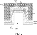
- FIG. 2 is an enlarged view of an area A of FIG. 1 .
- FIG. 3 is a cross-sectional view of a pixel structure of a display device according to an exemplary embodiment of the present disclosure.
- FIG. 4 is an enlarged view of an area B of FIG. 1 .
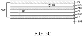
- FIGS. 5A to 5C are cross-sectional views for explaining overlapping between a power line and a connecting metal line of a display device according to an exemplary embodiment of the present disclosure.
- FIG. 6 is a view for explaining a capacitance compensating method of a display device according to an exemplary embodiment of the present disclosure.
- the substrate 110 includes a display area AA and a non-display area NA.
- the display area AA may include a first display area AA1 in which an irregularly shaped side is not disposed and a second display area AA2 in which an irregularly shaped side is disposed.
- the second display area AA2 may include a notch area NTA formed by the irregularly shaped side and include a second-first display area AA21 and a second-second display area AA22 which are divided to the left and the right by the notch area NTA.
- a plurality of pixels P is disposed in the first display area AA1 and the second display area AA2 and images may be displayed by the plurality of pixels P.
- the plurality of pixels P includes a thin film transistor TR, an organic light emitting diode OLED, a light blocking layer LS, a gate insulating layer GI, first and second insulating layers ILD1 and ILD2, a bank BNK, and an encapsulating layer EN.
- a buffer layer BUF is disposed on a substrate SUB which is formed of an insulating material such as transparent glass or plastic, and an active layer ACT which is formed of any one of polycrystalline silicon, low-temperature polysilicon, and an oxide semiconductor material is disposed thereon.
- the active layer ACT is formed of any one of polycrystalline silicon, low-temperature polysilicon, and an oxide semiconductor material and is a top-gate type
- the light blocking layer LS is disposed below the active layer ACT to block the influence on the characteristic of the thin film transistor TR due to external light.
- the light blocking layer LS may be formed of a low resistance opaque conductive material which may block the light.
- the light blocking layer LS may be formed of aluminum based metal such as aluminum (Al) or aluminum alloy (Al alloy), a silver based metal such as silver (Ag) or silver alloy, a copper based metal such as copper (Cu) or copper alloy, a molybdenum based metal such as molybdenum (Mo) or molybdenum alloy, or a low resistance opaque conductive material such as chrome (Cr), tantalum (Ta), or a titanium (Ti).
- the gate insulating layer GI is disposed on the substrate SUB including the light blocking layer LS and the active layer ACT.
- the gate insulating layer GI is a layer for insulating the active layer ACT from the gate electrode GE and may be configured by a single layer or multiple layers of an insulating material, for example, a silicon nitride layer SiNx or a silicon oxide layer SiO2, but is not limited thereto.
- the gate electrode GE is disposed on the gate insulating layer GI.
- the gate electrode GE is disposed above the active layer ACT.
- the gate electrode GE may be formed of a low resistance opaque conductive material.
- the gate electrode GE may be formed of an aluminum based metal such as aluminum (Al) or aluminum alloy (Al alloy), a silver based metal such as silver (Ag) or silver alloy, a copper based metal such as copper (Cu) or copper alloy, a molybdenum based metal such as molybdenum (Mo) or molybdenum alloy, or a low resistance opaque conductive material such as chrome (Cr), tantalum (Ta), or a titanium (Ti).
- a first insulating layer ILD1 which is formed of an insulating material is disposed on the gate electrode GE.
- a source electrode SE and a drain electrode DE which is spaced apart from the source electrode SE are disposed on the first insulating layer ILD1.
- the source electrode SE and the drain electrode DE are electrically connected to the active layer ACT through contact holes formed in the gate insulating layer GI and the first insulating layer ILD1.
- the source electrode SE and the drain electrode DE may be formed of an aluminum based metal such as aluminum (Al) or aluminum alloy (Al alloy), a silver based metal such as silver (Ag) or silver alloy, a copper based metal such as copper (Cu) or copper alloy, a molybdenum based metal such as molybdenum (Mo) or molybdenum alloy, or a low resistance opaque conductive material such as chrome (Cr), tantalum (Ta), or a titanium (Ti).
- the thin film transistor TR including the active layer ACT, the gate electrode GE, the source electrode SE, and the drain electrode DE is disposed on the substrate SUB.
- the second insulating layer ILD2 formed of an insulating material is disposed on the source electrode SE and the drain electrode DE and a planarization layer PAC is disposed on the second insulating layer ILD2.
- the planarization layer PAC may be formed of an organic insulating material, for example, an organic material which may planarize an upper surface, such as polyimide.
- a first electrode E1 and a bank BNK are disposed on the planarization layer PAC.
- the first electrode E1 may be an anode and is electrically connected to the drain electrode DE through contact holes formed on the second insulating layer ILD2 and the planarization layer PAC. Even though not illustrated, a reflective layer may be further disposed below the first electrode E1.
- the bank BNK may be disposed to cover a part of both sides of the first electrode E1 and may define an emission area where an organic light emitting layer EML is disposed to emit light. That is, the bank BNK is formed of an insulating material and the organic light emitting layer EML is disposed in an opening of the bank BNK to emit light. The organic light emitting layer EML is disposed on the first electrode E1 which is partially exposed by the bank BNK.
- the organic light emitting layer EML may include a hole injection layer, a hole transport layer, a light emitting layer, an electron transport layer, and an electron injection layer.
- a second electrode E2 is disposed above the organic light emitting layer EML and the bank BNK.
- the second electrode E2 may be a cathode and may be formed of a transparent conductive material.
- the transparent conductive material may consist of tin oxide (TO), indium tin oxide (ITO), indium zinc oxide (IZO), or indium zinc tin oxide (ITZO), but is not limited thereto.
- Such a second electrode E2 may form the organic light emitting diode OLED together with the first electrode E1 and the organic light emitting layer EML.
- the encapsulating layer EN is disposed above the organic light emitting diode OLED so as to protect the organic light emitting diode OLED and suppress foreign substances which may be generated from the outside or during the process from entering the organic light emitting diode OLED.
- the encapsulating layer EN may have a structure in which a plurality of inorganic layers and a plurality of organic layers are alternately disposed.
- a pixel including an organic light emitting diode OLED is described as an example, it is not limited thereto and the pixel may include a liquid crystal element.
- the second display area AA2 of the display area AA in which the plurality of pixels P is disposed has a concave portion defined by a shape of the irregularly shaped side. That is, as illustrated in FIGs. 1 and 2 , the second display area AA2 of the display area AA may have a notch area NTA which is inwardly recessed.
- the notch area NTA may be a non-display area NA in which pixels are not disposed, as described above.
- the gate lines GL disposed in the second display area AA2 are shorter than the gate lines GL disposed in the first display area AA1, due to the notch area NTA. Therefore, there may be a difference between the scan load amount of the first display area AA1 and the scan load amount of the second display area AA2.
- a data signal output from the data driver 120 that is, a data voltage is equally applied to the first display area AA1 and the second display area AA2. Therefore, in the display device including an irregularly shaped side, a scan load difference may be caused in accordance with a length difference of the gate lines so that the luminance of the first display area AA1 and the luminance of the second display area AA2 may be different from each other. More specifically, the luminance of the second display area AA2 is lower than the luminance of the first display area AA1 so as to be recognized as a stain.
- a scan load compensating pattern may be disposed to compensate the scan loads of the plurality of gate lines GL disposed in the second display area AA2.
- the scan load compensating pattern may be a plurality of connecting metal lines CML which electrically connects the gate lines GL of the second display area AA2 divided by the notch area NTA, in the notch area NTA.
- an active layer or a gate line which compensates the capacitance may be disposed in addition to the connecting metal line CML disposed in the notch area NTA. This will be described in more detail with reference to FIGS. 5A to 5C .
- the plurality of connecting metal lines CML electrically connects a gate line GL of the second-first display area AA21 and a gate line GL of the second-second display area AA22 which are divided by the notch area NTA.
- the plurality of connecting metal lines CML may be disposed in accordance with the shape of the notch area NTA. That is, the plurality of connecting metal lines CML may be disposed in accordance with the shape of the concave portion formed in the second display area AA2. Therefore, as illustrated in FIG. 4 , the plurality of connecting metal lines CML may be disposed to have a stepped shape in an area B which is curved in accordance with the shape of the concave portion.
- the plurality of connecting metal lines CML is disposed to have a stepped shape in the curved area so that the connecting metal lines CML which may compensate the scan load may be disposed without widening the non-display area NA.
- the plurality of connecting metal lines CML may be disposed to overlap the high-potential power link line area VDDA or the low-potential power link line area VSSA.
- the connecting metal lines CML are formed of the same material as the gate lines GL of the first and second display areas AA1 and AA2. Further, the connecting metal lines CML are formed on the same layer as the layer on which the gate lines GL are disposed.
- the connecting metal line CML may form a first capacitance C1 together with the power line PL which is the high-potential power link line or the low-potential power link line disposed on the first insulating layer ILD1.
- the power line PL may be formed of the same material as the data line DL disposed in the first and second display areas AA1 and AA2 and may be disposed on the same layer.
- the connecting metal lines CML which electrically connect the gate lines GL of the second display area AA2 which are divided by the arrangement of the notch area NTA are disposed.
- the connecting metal lines CML overlap the power line PL which is the high-potential power link line or the low-potential power link line to form a capacitance. Therefore, an RC delay is equal to that of the first display area AA1 so that the luminance irregularity of the display device 100 due to the scan load difference may be minimized.
- the RC delay of the first display area AA1 is set as a reference value and an RC delay of the second display area AA2 including the notch area NTA is compared with the reference value.
- a scan load compensating pattern which may form a capacitance together with the connecting metal line CML disposed in the notch area NTA, that is, a capacitance compensating pattern may be further disposed.
- an RC delay of the first display area AA1 is calculated to be set as a reference value.
- an RC delay ⁇ of the first display area AA1 that is, an RC delay of a reference area ( ⁇ of ref. area)
- 72190.5137 Since the RC delay ⁇ of the reference area (ref.) is a reference value and an RC delay ⁇ of the notch area A ( ⁇ obtained by considering number of pixels of notch area) is 4.00E+04, the RC delay which needs to be compensated is 32182.70926.
- the converted capacitance (converted Cap which needs to be compensated) value is determined to be 7194.985557.
- the lengths of the gate lines GL of the second display area AA2 which vary due to the formation of the notch area NTA and a result the scan loads of the pixels increases going from notch area A to notch area E of FIG. 6 .
- the difference may be converted to a capacitance which needs to be compensated.
- the capacitance converted as described above may improve the RC delay of the second display area AA2 and may be implemented by additionally forming a compensating pattern which may form a capacitance together with the connecting metal line disposed in the notch area NTA to minimize deterioration of an image quality of the display device 100 due to the arrangement of the irregularly shaped side.
- active layers ACT of the first and second display areas AA1 and AA2 are additionally disposed below the gate insulating layer GI to further form a capacitance and a contact hole CNT is formed in the gate insulating layer GI to electrically connect the power line PL and the active layer ACT through the contact hole CNT. Therefore, a second capacitance C2 may be formed in addition to the first capacitance C1 of FIG. 5A .
- the light blocking layer LS disposed in the first display area AA1 and AA2 disposed on the substrate SUB is additionally disposed and the power line PL and the light blocking layer LS are electrically connected through the contact hole CNT disposed in the buffer layer BUF and the gate insulating layer GI. Therefore, in addition to the first capacitance C1 of FIG. 5A , the second capacitance C2 may be formed.
- the light blocking layer LS, the active layer ACT, and the connecting metal line CML are disposed on different layers with an insulating layer therebetween. Therefore, in order to compensate the capacitance, all the light blocking layer LS, the active layer ACT, and the connecting metal line CML may be disposed to overlap each other.
- the capacitance compensating pattern As described above, in the display device 100 according to the exemplary embodiment of the present disclosure, as the capacitance compensating pattern, the active layer ACT or the light blocking layer LS is further disposed in the notch area NTA and formed on a same layer as the active layer ACT or the light blocking layer LS of the display area to form the capacitance to be equal to the reference value. Therefore, the capacitance compensating pattern may be disposed in the notch area NTA without adding a separate mask.
- a compensating pattern is formed to compensate the capacitance such that the RC delay which varies due to the formation of the irregularly shaped side becomes equal to the RC delay of the display area where the irregularly shaped side is not formed. Therefore, the luminance irregularity of the display device may be reduced.
- a display device includes: a substrate which includes a display area having an irregularly shaped side and a non-display area which includes a notch area defined by a shape of the irregularly shaped side of the display area and is disposed to enclose the display area; a plurality of gate lines which is divided to be disposed in a left display area of the display area and a right display area of the display area due to the irregularly shaped side of the display area; and a connecting metal line which connects the plurality of gate lines divided to be disposed in the left display area and the right display area in the notch area.
- the connecting metal line may be disposed in accordance with an irregularly shaped structure due to the irregularly shaped side.
- the connecting metal line may be disposed to have a stepped shape in an area where the irregularly shaped structure due to the irregularly shaped side is curved.
- a plurality of high-potential power link lines and a plurality of low-potential power link lines may be further disposed to supply a high-potential power and a low-potential power to the display area.
- the connecting metal line may be disposed on a different layer from that of the plurality of high-potential power link lines and the plurality of low-potential power link lines.
- the connecting metal line may overlap the plurality of high-potential power link lines and the plurality of low-potential power link lines.
- a capacitance compensating pattern may be further disposed to compensate a capacitance of the display area having the irregularly shaped side.
- the capacitance compensating pattern may be an active layer or a light blocking layer disposed in the display area.
- the capacitance compensating pattern may be adapted such that an RC delay of the display area which does not have the irregularly shaped side is set as a reference value and an RC delay of the display area having the irregularly shaped side is calculated to be equal to the reference value.
- images may be displayed.
- a plurality of pixels may be disposed in the display area.
- the plurality of gate lines may be adapted to apply a gate signal to the plurality of pixels.
- the gate lines may be disposed to be divided due to one or more irregularly shaped sides among four sides of the display area.
- the display device may include a plurality of power lines which are adapted to apply a high-potential power and a low-potential power to the plurality of pixels.
- the display device may include a plurality of connecting metal lines that may be disposed below the plurality of power lines and may connect the plurality of gate lines which are disposed to be divided due to the one or more irregularly shaped side.
- the display device may include a capacitance compensating pattern that may be disposed below the plurality of connecting metal lines.
- the number of pixels disposed in a portion of the display area where an irregularly shaped side is formed may be different from the number of pixels disposed in a portion of the display area where an irregularly shaped side is not formed, due to the one or more irregularly shaped sides disposed in the display area.
- An RC delay may vary depending on the number of pixels.
- the capacitance compensating pattern may be adapted to compensate a capacitance of the display area where the one or more irregularly shaped sides are formed based on the RC delay of the display area where the one or more irregularly shaped sides are not formed.
- the capacitance compensating pattern may be electrically connected to the plurality of power lines.
- a display device may include a plurality of pixels disposed in a display area where images are displayed, a plurality of gate lines which apply a gate signal to the plurality of pixels and are disposed to be divided due to one or more irregularly shaped sides among four sides of the display area, a plurality of power lines which apply a high-potential power and a low-potential power to the plurality of pixels, a plurality of connecting metal lines which are disposed below the plurality of power lines and connect the plurality of gate lines which are disposed to be divided due to the irregularly shaped side, and a capacitance compensating pattern disposed below the plurality of connecting metal lines.
- the number of pixels disposed in a portion of the display area where an irregularly shaped side is formed may be different from the number of pixels disposed in a portion of the display area where an irregularly shaped side is not formed, due to the one or more irregularly shaped sides disposed in the display area.
- An RC delay may vary depending on the number of pixels.
- the capacitance compensating pattern may compensate a capacitance of the display area where the irregularly shaped side is formed based on the RC delay of the display area where the irregularly shaped side is not formed.
- the capacitance compensating pattern may be electrically connected to the plurality of power lines.
Landscapes
- Engineering & Computer Science (AREA)
- Microelectronics & Electronic Packaging (AREA)
- Physics & Mathematics (AREA)
- Computer Hardware Design (AREA)
- General Physics & Mathematics (AREA)
- Theoretical Computer Science (AREA)
- Geometry (AREA)
- Devices For Indicating Variable Information By Combining Individual Elements (AREA)
- Electroluminescent Light Sources (AREA)
Applications Claiming Priority (1)
| Application Number | Priority Date | Filing Date | Title |
|---|---|---|---|
| KR1020170170343A KR102509413B1 (ko) | 2017-12-12 | 2017-12-12 | 표시 장치 |
Publications (3)
| Publication Number | Publication Date |
|---|---|
| EP3499490A2 true EP3499490A2 (de) | 2019-06-19 |
| EP3499490A3 EP3499490A3 (de) | 2019-07-17 |
| EP3499490B1 EP3499490B1 (de) | 2023-07-26 |
Family
ID=64606850
Family Applications (1)
| Application Number | Title | Priority Date | Filing Date |
|---|---|---|---|
| EP18210419.0A Active EP3499490B1 (de) | 2017-12-12 | 2018-12-05 | Anzeigevorrichtung |
Country Status (4)
| Country | Link |
|---|---|
| US (1) | US10748978B2 (de) |
| EP (1) | EP3499490B1 (de) |
| KR (1) | KR102509413B1 (de) |
| CN (1) | CN110010622B (de) |
Cited By (1)
| Publication number | Priority date | Publication date | Assignee | Title |
|---|---|---|---|---|
| WO2021126597A3 (en) * | 2019-12-19 | 2021-07-29 | Google Llc | Power line design for sensors in display panel |
Families Citing this family (26)
| Publication number | Priority date | Publication date | Assignee | Title |
|---|---|---|---|---|
| KR102362704B1 (ko) | 2017-09-07 | 2022-02-14 | 삼성디스플레이 주식회사 | 유기 발광 표시 장치 |
| CN107978622B (zh) * | 2017-11-22 | 2020-08-11 | 上海天马有机发光显示技术有限公司 | 一种阵列基板、显示面板和显示装置 |
| KR102509257B1 (ko) * | 2017-12-11 | 2023-03-10 | 엘지디스플레이 주식회사 | 표시 장치 |
| KR102587861B1 (ko) | 2018-03-27 | 2023-10-12 | 삼성디스플레이 주식회사 | 표시 장치 및 이의 제조 방법 |
| US11538894B2 (en) * | 2018-03-30 | 2022-12-27 | Sharp Kabushiki Kaisha | Display device with overlapped wiring lines at periphery of cutout region |
| KR102525343B1 (ko) * | 2018-04-09 | 2023-04-26 | 삼성디스플레이 주식회사 | 유기 발광 표시 장치 |
| KR102649144B1 (ko) * | 2018-06-25 | 2024-03-21 | 삼성디스플레이 주식회사 | 디스플레이 장치 |
| CN109061975A (zh) * | 2018-10-26 | 2018-12-21 | 昆山国显光电有限公司 | 一种显示装置及其显示面板 |
| KR102856587B1 (ko) * | 2019-07-03 | 2025-09-08 | 삼성디스플레이 주식회사 | 표시장치 |
| US11074856B2 (en) * | 2019-08-09 | 2021-07-27 | Wuhan China Star Optoelectronics Semiconductor Display Technology Co., Ltd. | Display panel and display device |
| CN110459572B (zh) * | 2019-08-19 | 2023-01-06 | 京东方科技集团股份有限公司 | 显示面板 |
| CN112750844B (zh) * | 2019-10-30 | 2025-10-31 | 京东方科技集团股份有限公司 | 显示基板和显示装置 |
| US11393890B2 (en) * | 2020-01-09 | 2022-07-19 | Wuhan China Optoelectronics Semiconductor Display Technology Co., Ltd. | Active matrix organic light-emitting diode display panel with compensation capacitor |
| CN114930435B (zh) * | 2020-01-20 | 2023-08-22 | 夏普株式会社 | 显示装置 |
| US12082460B2 (en) * | 2020-02-27 | 2024-09-03 | Chengdu Boe Optoelectronics Technology Co., Ltd. | Display substrate and manufacturing method thereof, and display apparatus |
| EP4113495B1 (de) * | 2020-02-27 | 2025-10-29 | BOE Technology Group Co., Ltd. | Anzeigesubstrat und verfahren zu seiner herstellung sowie verfahren zur kompensation der verdrahtungslast |
| KR102781578B1 (ko) | 2020-03-30 | 2025-03-18 | 삼성디스플레이 주식회사 | 디스플레이 장치 |
| CN111446284A (zh) * | 2020-05-07 | 2020-07-24 | 武汉华星光电半导体显示技术有限公司 | Oled显示面板及其制作方法 |
| US11087663B1 (en) * | 2020-05-15 | 2021-08-10 | Novatek Microelectronics Corp. | Display device and driving method thereof for reducing difference in brightness between areas with different widths |
| KR102759953B1 (ko) * | 2020-06-02 | 2025-01-24 | 삼성디스플레이 주식회사 | 표시 장치 |
| US11545537B2 (en) | 2020-06-15 | 2023-01-03 | Samsung Display Co., Ltd. | Display device |
| CN114341965B (zh) * | 2020-07-30 | 2023-11-28 | 京东方科技集团股份有限公司 | 显示基板及其制备方法、显示装置 |
| CN114464644B (zh) | 2020-11-09 | 2025-03-21 | 京东方科技集团股份有限公司 | 显示基板和显示装置 |
| KR20220145948A (ko) | 2021-04-20 | 2022-10-31 | 삼성디스플레이 주식회사 | 표시 장치 |
| CN113554969B (zh) * | 2021-07-16 | 2024-04-12 | 武汉天马微电子有限公司 | 显示面板及显示装置 |
| CN116110909A (zh) * | 2022-12-26 | 2023-05-12 | 京东方科技集团股份有限公司 | 显示基板和显示装置 |
Family Cites Families (9)
| Publication number | Priority date | Publication date | Assignee | Title |
|---|---|---|---|---|
| KR101839334B1 (ko) * | 2011-12-07 | 2018-03-19 | 엘지디스플레이 주식회사 | 액정 표시장치 및 그 제조방법 |
| CN105742312B (zh) * | 2014-12-31 | 2019-02-12 | 乐金显示有限公司 | 有机发光显示装置 |
| CN104898343B (zh) * | 2015-06-30 | 2017-12-22 | 重庆京东方光电科技有限公司 | 阵列基板、显示面板及显示装置 |
| KR102387786B1 (ko) * | 2015-07-28 | 2022-04-15 | 엘지디스플레이 주식회사 | 백플레인 기판 및 이를 이용한 플렉서블 디스플레이 |
| WO2017172375A1 (en) | 2016-03-28 | 2017-10-05 | Groturbel Research Llc | Light-emitting diode displays |
| US10354578B2 (en) * | 2016-04-15 | 2019-07-16 | Samsung Display Co., Ltd. | Display device |
| KR102666831B1 (ko) * | 2016-04-15 | 2024-05-21 | 삼성디스플레이 주식회사 | 표시 장치 |
| CN107221536B (zh) * | 2017-05-25 | 2019-12-13 | 上海天马微电子有限公司 | 阵列基板、异形显示器及显示装置 |
| CN107342036B (zh) | 2017-08-21 | 2020-10-30 | 厦门天马微电子有限公司 | 显示面板及显示装置 |
-
2017
- 2017-12-12 KR KR1020170170343A patent/KR102509413B1/ko active Active
-
2018
- 2018-12-05 US US16/211,073 patent/US10748978B2/en active Active
- 2018-12-05 EP EP18210419.0A patent/EP3499490B1/de active Active
- 2018-12-07 CN CN201811495274.7A patent/CN110010622B/zh active Active
Non-Patent Citations (1)
| Title |
|---|
| None |
Cited By (1)
| Publication number | Priority date | Publication date | Assignee | Title |
|---|---|---|---|---|
| WO2021126597A3 (en) * | 2019-12-19 | 2021-07-29 | Google Llc | Power line design for sensors in display panel |
Also Published As
| Publication number | Publication date |
|---|---|
| EP3499490A3 (de) | 2019-07-17 |
| EP3499490B1 (de) | 2023-07-26 |
| CN110010622B (zh) | 2023-06-02 |
| US10748978B2 (en) | 2020-08-18 |
| KR20190069955A (ko) | 2019-06-20 |
| KR102509413B1 (ko) | 2023-03-10 |
| CN110010622A (zh) | 2019-07-12 |
| US20190181213A1 (en) | 2019-06-13 |
Similar Documents
| Publication | Publication Date | Title |
|---|---|---|
| US10748978B2 (en) | Display device | |
| KR102703706B1 (ko) | 표시 장치 | |
| KR102893375B1 (ko) | 표시 장치 | |
| US10930723B2 (en) | Display device | |
| KR102799511B1 (ko) | 표시 장치 | |
| KR102921529B1 (ko) | 표시 패널 | |
| US11262967B2 (en) | Display device and tiled display device including the same | |
| US12213352B2 (en) | Display device including a lower metal line overlapping driving transistor or switching transistor to minimize crosstalk | |
| KR20190002884A (ko) | 트랜지스터 기판 및 이를 이용한 표시패널 | |
| KR20220095833A (ko) | 표시 장치 | |
| GB2624970A (en) | Display device | |
| KR102242350B1 (ko) | 유기발광 디스플레이 장치 | |
| KR20230082168A (ko) | 표시 장치 및 표시 패널 | |
| KR20230082149A (ko) | 표시패널 및 표시 장치 | |
| US20250185494A1 (en) | Display device | |
| US20250386711A1 (en) | Display device, electronic device including the same, and method for manufacturing the same | |
| US20250046242A1 (en) | Display device | |
| US20240222385A1 (en) | Display device | |
| EP4557912A1 (de) | Anzeigevorrichtung | |
| US20250089530A1 (en) | Display device and method of fabricating the same | |
| US20260006989A1 (en) | Display device and method for fabricating the same | |
| US20240224621A1 (en) | Display device | |
| CN118234308A (zh) | 有机发光显示装置 | |
| CN118414654A (zh) | 阵列基板和显示装置 | |
| KR20260063090A (ko) | 회로부 및 발광부를 포함하는 표시장치 |
Legal Events
| Date | Code | Title | Description |
|---|---|---|---|
| PUAI | Public reference made under article 153(3) epc to a published international application that has entered the european phase |
Free format text: ORIGINAL CODE: 0009012 |
|
| STAA | Information on the status of an ep patent application or granted ep patent |
Free format text: STATUS: REQUEST FOR EXAMINATION WAS MADE |
|
| PUAL | Search report despatched |
Free format text: ORIGINAL CODE: 0009013 |
|
| 17P | Request for examination filed |
Effective date: 20181205 |
|
| AK | Designated contracting states |
Kind code of ref document: A2 Designated state(s): AL AT BE BG CH CY CZ DE DK EE ES FI FR GB GR HR HU IE IS IT LI LT LU LV MC MK MT NL NO PL PT RO RS SE SI SK SM TR |
|
| AX | Request for extension of the european patent |
Extension state: BA ME |
|
| AK | Designated contracting states |
Kind code of ref document: A3 Designated state(s): AL AT BE BG CH CY CZ DE DK EE ES FI FR GB GR HR HU IE IS IT LI LT LU LV MC MK MT NL NO PL PT RO RS SE SI SK SM TR |
|
| AX | Request for extension of the european patent |
Extension state: BA ME |
|
| RIC1 | Information provided on ipc code assigned before grant |
Ipc: H01L 27/32 20060101ALI20190607BHEP Ipc: G09G 3/3225 20160101ALI20190607BHEP Ipc: G09G 3/20 20060101AFI20190607BHEP |
|
| RBV | Designated contracting states (corrected) |
Designated state(s): AL AT BE BG CH CY CZ DE DK EE ES FI FR GB GR HR HU IE IS IT LI LT LU LV MC MK MT NL NO PL PT RO RS SE SI SK SM TR |
|
| STAA | Information on the status of an ep patent application or granted ep patent |
Free format text: STATUS: EXAMINATION IS IN PROGRESS |
|
| 17Q | First examination report despatched |
Effective date: 20211207 |
|
| GRAP | Despatch of communication of intention to grant a patent |
Free format text: ORIGINAL CODE: EPIDOSNIGR1 |
|
| STAA | Information on the status of an ep patent application or granted ep patent |
Free format text: STATUS: GRANT OF PATENT IS INTENDED |
|
| RIC1 | Information provided on ipc code assigned before grant |
Ipc: G09G 3/3225 20160101ALI20230119BHEP Ipc: G09G 3/20 20060101AFI20230119BHEP |
|
| INTG | Intention to grant announced |
Effective date: 20230221 |
|
| GRAS | Grant fee paid |
Free format text: ORIGINAL CODE: EPIDOSNIGR3 |
|
| GRAA | (expected) grant |
Free format text: ORIGINAL CODE: 0009210 |
|
| STAA | Information on the status of an ep patent application or granted ep patent |
Free format text: STATUS: THE PATENT HAS BEEN GRANTED |
|
| AK | Designated contracting states |
Kind code of ref document: B1 Designated state(s): AL AT BE BG CH CY CZ DE DK EE ES FI FR GB GR HR HU IE IS IT LI LT LU LV MC MK MT NL NO PL PT RO RS SE SI SK SM TR |
|
| REG | Reference to a national code |
Ref country code: CH Ref legal event code: EP |
|
| REG | Reference to a national code |
Ref country code: DE Ref legal event code: R096 Ref document number: 602018053969 Country of ref document: DE |
|
| REG | Reference to a national code |
Ref country code: IE Ref legal event code: FG4D |
|
| REG | Reference to a national code |
Ref country code: LT Ref legal event code: MG9D |
|
| REG | Reference to a national code |
Ref country code: NL Ref legal event code: MP Effective date: 20230726 |
|
| REG | Reference to a national code |
Ref country code: AT Ref legal event code: MK05 Ref document number: 1592872 Country of ref document: AT Kind code of ref document: T Effective date: 20230726 |
|
| PG25 | Lapsed in a contracting state [announced via postgrant information from national office to epo] |
Ref country code: NL Free format text: LAPSE BECAUSE OF FAILURE TO SUBMIT A TRANSLATION OF THE DESCRIPTION OR TO PAY THE FEE WITHIN THE PRESCRIBED TIME-LIMIT Effective date: 20230726 |
|
| PG25 | Lapsed in a contracting state [announced via postgrant information from national office to epo] |
Ref country code: GR Free format text: LAPSE BECAUSE OF FAILURE TO SUBMIT A TRANSLATION OF THE DESCRIPTION OR TO PAY THE FEE WITHIN THE PRESCRIBED TIME-LIMIT Effective date: 20231027 |
|
| PG25 | Lapsed in a contracting state [announced via postgrant information from national office to epo] |
Ref country code: IS Free format text: LAPSE BECAUSE OF FAILURE TO SUBMIT A TRANSLATION OF THE DESCRIPTION OR TO PAY THE FEE WITHIN THE PRESCRIBED TIME-LIMIT Effective date: 20231126 |
|
| PG25 | Lapsed in a contracting state [announced via postgrant information from national office to epo] |
Ref country code: SE Free format text: LAPSE BECAUSE OF FAILURE TO SUBMIT A TRANSLATION OF THE DESCRIPTION OR TO PAY THE FEE WITHIN THE PRESCRIBED TIME-LIMIT Effective date: 20230726 Ref country code: RS Free format text: LAPSE BECAUSE OF FAILURE TO SUBMIT A TRANSLATION OF THE DESCRIPTION OR TO PAY THE FEE WITHIN THE PRESCRIBED TIME-LIMIT Effective date: 20230726 Ref country code: PT Free format text: LAPSE BECAUSE OF FAILURE TO SUBMIT A TRANSLATION OF THE DESCRIPTION OR TO PAY THE FEE WITHIN THE PRESCRIBED TIME-LIMIT Effective date: 20231127 Ref country code: NO Free format text: LAPSE BECAUSE OF FAILURE TO SUBMIT A TRANSLATION OF THE DESCRIPTION OR TO PAY THE FEE WITHIN THE PRESCRIBED TIME-LIMIT Effective date: 20231026 Ref country code: LV Free format text: LAPSE BECAUSE OF FAILURE TO SUBMIT A TRANSLATION OF THE DESCRIPTION OR TO PAY THE FEE WITHIN THE PRESCRIBED TIME-LIMIT Effective date: 20230726 Ref country code: LT Free format text: LAPSE BECAUSE OF FAILURE TO SUBMIT A TRANSLATION OF THE DESCRIPTION OR TO PAY THE FEE WITHIN THE PRESCRIBED TIME-LIMIT Effective date: 20230726 Ref country code: IS Free format text: LAPSE BECAUSE OF FAILURE TO SUBMIT A TRANSLATION OF THE DESCRIPTION OR TO PAY THE FEE WITHIN THE PRESCRIBED TIME-LIMIT Effective date: 20231126 Ref country code: HR Free format text: LAPSE BECAUSE OF FAILURE TO SUBMIT A TRANSLATION OF THE DESCRIPTION OR TO PAY THE FEE WITHIN THE PRESCRIBED TIME-LIMIT Effective date: 20230726 Ref country code: GR Free format text: LAPSE BECAUSE OF FAILURE TO SUBMIT A TRANSLATION OF THE DESCRIPTION OR TO PAY THE FEE WITHIN THE PRESCRIBED TIME-LIMIT Effective date: 20231027 Ref country code: FI Free format text: LAPSE BECAUSE OF FAILURE TO SUBMIT A TRANSLATION OF THE DESCRIPTION OR TO PAY THE FEE WITHIN THE PRESCRIBED TIME-LIMIT Effective date: 20230726 Ref country code: AT Free format text: LAPSE BECAUSE OF FAILURE TO SUBMIT A TRANSLATION OF THE DESCRIPTION OR TO PAY THE FEE WITHIN THE PRESCRIBED TIME-LIMIT Effective date: 20230726 |
|
| PG25 | Lapsed in a contracting state [announced via postgrant information from national office to epo] |
Ref country code: PL Free format text: LAPSE BECAUSE OF FAILURE TO SUBMIT A TRANSLATION OF THE DESCRIPTION OR TO PAY THE FEE WITHIN THE PRESCRIBED TIME-LIMIT Effective date: 20230726 |
|
| PG25 | Lapsed in a contracting state [announced via postgrant information from national office to epo] |
Ref country code: ES Free format text: LAPSE BECAUSE OF FAILURE TO SUBMIT A TRANSLATION OF THE DESCRIPTION OR TO PAY THE FEE WITHIN THE PRESCRIBED TIME-LIMIT Effective date: 20230726 |
|
| REG | Reference to a national code |
Ref country code: DE Ref legal event code: R097 Ref document number: 602018053969 Country of ref document: DE |
|
| PG25 | Lapsed in a contracting state [announced via postgrant information from national office to epo] |
Ref country code: SM Free format text: LAPSE BECAUSE OF FAILURE TO SUBMIT A TRANSLATION OF THE DESCRIPTION OR TO PAY THE FEE WITHIN THE PRESCRIBED TIME-LIMIT Effective date: 20230726 Ref country code: RO Free format text: LAPSE BECAUSE OF FAILURE TO SUBMIT A TRANSLATION OF THE DESCRIPTION OR TO PAY THE FEE WITHIN THE PRESCRIBED TIME-LIMIT Effective date: 20230726 Ref country code: ES Free format text: LAPSE BECAUSE OF FAILURE TO SUBMIT A TRANSLATION OF THE DESCRIPTION OR TO PAY THE FEE WITHIN THE PRESCRIBED TIME-LIMIT Effective date: 20230726 Ref country code: EE Free format text: LAPSE BECAUSE OF FAILURE TO SUBMIT A TRANSLATION OF THE DESCRIPTION OR TO PAY THE FEE WITHIN THE PRESCRIBED TIME-LIMIT Effective date: 20230726 Ref country code: DK Free format text: LAPSE BECAUSE OF FAILURE TO SUBMIT A TRANSLATION OF THE DESCRIPTION OR TO PAY THE FEE WITHIN THE PRESCRIBED TIME-LIMIT Effective date: 20230726 Ref country code: CZ Free format text: LAPSE BECAUSE OF FAILURE TO SUBMIT A TRANSLATION OF THE DESCRIPTION OR TO PAY THE FEE WITHIN THE PRESCRIBED TIME-LIMIT Effective date: 20230726 Ref country code: SK Free format text: LAPSE BECAUSE OF FAILURE TO SUBMIT A TRANSLATION OF THE DESCRIPTION OR TO PAY THE FEE WITHIN THE PRESCRIBED TIME-LIMIT Effective date: 20230726 |
|
| PG25 | Lapsed in a contracting state [announced via postgrant information from national office to epo] |
Ref country code: IT Free format text: LAPSE BECAUSE OF FAILURE TO SUBMIT A TRANSLATION OF THE DESCRIPTION OR TO PAY THE FEE WITHIN THE PRESCRIBED TIME-LIMIT Effective date: 20230726 |
|
| PLBE | No opposition filed within time limit |
Free format text: ORIGINAL CODE: 0009261 |
|
| STAA | Information on the status of an ep patent application or granted ep patent |
Free format text: STATUS: NO OPPOSITION FILED WITHIN TIME LIMIT |
|
| 26N | No opposition filed |
Effective date: 20240429 |
|
| PG25 | Lapsed in a contracting state [announced via postgrant information from national office to epo] |
Ref country code: SI Free format text: LAPSE BECAUSE OF FAILURE TO SUBMIT A TRANSLATION OF THE DESCRIPTION OR TO PAY THE FEE WITHIN THE PRESCRIBED TIME-LIMIT Effective date: 20230726 |
|
| REG | Reference to a national code |
Ref country code: CH Ref legal event code: PL |
|
| PG25 | Lapsed in a contracting state [announced via postgrant information from national office to epo] |
Ref country code: LU Free format text: LAPSE BECAUSE OF NON-PAYMENT OF DUE FEES Effective date: 20231205 |
|
| PG25 | Lapsed in a contracting state [announced via postgrant information from national office to epo] |
Ref country code: MC Free format text: LAPSE BECAUSE OF FAILURE TO SUBMIT A TRANSLATION OF THE DESCRIPTION OR TO PAY THE FEE WITHIN THE PRESCRIBED TIME-LIMIT Effective date: 20230726 |
|
| REG | Reference to a national code |
Ref country code: BE Ref legal event code: MM Effective date: 20231231 |
|
| PG25 | Lapsed in a contracting state [announced via postgrant information from national office to epo] |
Ref country code: MC Free format text: LAPSE BECAUSE OF FAILURE TO SUBMIT A TRANSLATION OF THE DESCRIPTION OR TO PAY THE FEE WITHIN THE PRESCRIBED TIME-LIMIT Effective date: 20230726 Ref country code: LU Free format text: LAPSE BECAUSE OF NON-PAYMENT OF DUE FEES Effective date: 20231205 |
|
| REG | Reference to a national code |
Ref country code: IE Ref legal event code: MM4A |
|
| PG25 | Lapsed in a contracting state [announced via postgrant information from national office to epo] |
Ref country code: IE Free format text: LAPSE BECAUSE OF NON-PAYMENT OF DUE FEES Effective date: 20231205 |
|
| PG25 | Lapsed in a contracting state [announced via postgrant information from national office to epo] |
Ref country code: BE Free format text: LAPSE BECAUSE OF NON-PAYMENT OF DUE FEES Effective date: 20231231 |
|
| PG25 | Lapsed in a contracting state [announced via postgrant information from national office to epo] |
Ref country code: CH Free format text: LAPSE BECAUSE OF NON-PAYMENT OF DUE FEES Effective date: 20231231 |
|
| PG25 | Lapsed in a contracting state [announced via postgrant information from national office to epo] |
Ref country code: IE Free format text: LAPSE BECAUSE OF NON-PAYMENT OF DUE FEES Effective date: 20231205 Ref country code: CH Free format text: LAPSE BECAUSE OF NON-PAYMENT OF DUE FEES Effective date: 20231231 Ref country code: BE Free format text: LAPSE BECAUSE OF NON-PAYMENT OF DUE FEES Effective date: 20231231 |
|
| PG25 | Lapsed in a contracting state [announced via postgrant information from national office to epo] |
Ref country code: BG Free format text: LAPSE BECAUSE OF FAILURE TO SUBMIT A TRANSLATION OF THE DESCRIPTION OR TO PAY THE FEE WITHIN THE PRESCRIBED TIME-LIMIT Effective date: 20230726 |
|
| PG25 | Lapsed in a contracting state [announced via postgrant information from national office to epo] |
Ref country code: BG Free format text: LAPSE BECAUSE OF FAILURE TO SUBMIT A TRANSLATION OF THE DESCRIPTION OR TO PAY THE FEE WITHIN THE PRESCRIBED TIME-LIMIT Effective date: 20230726 |
|
| PG25 | Lapsed in a contracting state [announced via postgrant information from national office to epo] |
Ref country code: CY Free format text: LAPSE BECAUSE OF FAILURE TO SUBMIT A TRANSLATION OF THE DESCRIPTION OR TO PAY THE FEE WITHIN THE PRESCRIBED TIME-LIMIT; INVALID AB INITIO Effective date: 20181205 |
|
| PG25 | Lapsed in a contracting state [announced via postgrant information from national office to epo] |
Ref country code: HU Free format text: LAPSE BECAUSE OF FAILURE TO SUBMIT A TRANSLATION OF THE DESCRIPTION OR TO PAY THE FEE WITHIN THE PRESCRIBED TIME-LIMIT; INVALID AB INITIO Effective date: 20181205 |
|
| PG25 | Lapsed in a contracting state [announced via postgrant information from national office to epo] |
Ref country code: TR Free format text: LAPSE BECAUSE OF FAILURE TO SUBMIT A TRANSLATION OF THE DESCRIPTION OR TO PAY THE FEE WITHIN THE PRESCRIBED TIME-LIMIT Effective date: 20230726 |
|
| PGFP | Annual fee paid to national office [announced via postgrant information from national office to epo] |
Ref country code: DE Payment date: 20251020 Year of fee payment: 8 |
|
| PGFP | Annual fee paid to national office [announced via postgrant information from national office to epo] |
Ref country code: GB Payment date: 20251023 Year of fee payment: 8 |
|
| PGFP | Annual fee paid to national office [announced via postgrant information from national office to epo] |
Ref country code: FR Payment date: 20251021 Year of fee payment: 8 |