EP3497752B1 - Elektrisches kontaktelement für einen elektrischen verbinder mit mikrostrukturierten hohlräumen unter der kontaktfläche - Google Patents
Elektrisches kontaktelement für einen elektrischen verbinder mit mikrostrukturierten hohlräumen unter der kontaktfläche Download PDFInfo
- Publication number
- EP3497752B1 EP3497752B1 EP17755097.7A EP17755097A EP3497752B1 EP 3497752 B1 EP3497752 B1 EP 3497752B1 EP 17755097 A EP17755097 A EP 17755097A EP 3497752 B1 EP3497752 B1 EP 3497752B1
- Authority
- EP
- European Patent Office
- Prior art keywords
- microstructure
- contact surface
- auxiliary material
- contact element
- electrically conductive
- Prior art date
- Legal status (The legal status is an assumption and is not a legal conclusion. Google has not performed a legal analysis and makes no representation as to the accuracy of the status listed.)
- Active
Links
Images

Classifications
-
- H—ELECTRICITY
- H01—ELECTRIC ELEMENTS
- H01R—ELECTRICALLY-CONDUCTIVE CONNECTIONS; STRUCTURAL ASSOCIATIONS OF A PLURALITY OF MUTUALLY-INSULATED ELECTRICAL CONNECTING ELEMENTS; COUPLING DEVICES; CURRENT COLLECTORS
- H01R13/00—Details of coupling devices of the kinds covered by groups H01R12/70 or H01R24/00 - H01R33/00
- H01R13/02—Contact members
- H01R13/03—Contact members characterised by the material, e.g. plating, or coating materials
-
- B—PERFORMING OPERATIONS; TRANSPORTING
- B32—LAYERED PRODUCTS
- B32B—LAYERED PRODUCTS, i.e. PRODUCTS BUILT-UP OF STRATA OF FLAT OR NON-FLAT, e.g. CELLULAR OR HONEYCOMB, FORM
- B32B15/00—Layered products comprising a layer of metal
- B32B15/01—Layered products comprising a layer of metal all layers being exclusively metallic
-
- B—PERFORMING OPERATIONS; TRANSPORTING
- B32—LAYERED PRODUCTS
- B32B—LAYERED PRODUCTS, i.e. PRODUCTS BUILT-UP OF STRATA OF FLAT OR NON-FLAT, e.g. CELLULAR OR HONEYCOMB, FORM
- B32B15/00—Layered products comprising a layer of metal
- B32B15/01—Layered products comprising a layer of metal all layers being exclusively metallic
- B32B15/018—Layered products comprising a layer of metal all layers being exclusively metallic one layer being formed of a noble metal or a noble metal alloy
-
- C—CHEMISTRY; METALLURGY
- C22—METALLURGY; FERROUS OR NON-FERROUS ALLOYS; TREATMENT OF ALLOYS OR NON-FERROUS METALS
- C22C—ALLOYS
- C22C9/00—Alloys based on copper
-
- H—ELECTRICITY
- H01—ELECTRIC ELEMENTS
- H01R—ELECTRICALLY-CONDUCTIVE CONNECTIONS; STRUCTURAL ASSOCIATIONS OF A PLURALITY OF MUTUALLY-INSULATED ELECTRICAL CONNECTING ELEMENTS; COUPLING DEVICES; CURRENT COLLECTORS
- H01R13/00—Details of coupling devices of the kinds covered by groups H01R12/70 or H01R24/00 - H01R33/00
- H01R13/46—Bases; Cases
- H01R13/533—Bases, cases made for use in extreme conditions, e.g. high temperature, radiation, vibration, corrosive environment, pressure
-
- H—ELECTRICITY
- H01—ELECTRIC ELEMENTS
- H01R—ELECTRICALLY-CONDUCTIVE CONNECTIONS; STRUCTURAL ASSOCIATIONS OF A PLURALITY OF MUTUALLY-INSULATED ELECTRICAL CONNECTING ELEMENTS; COUPLING DEVICES; CURRENT COLLECTORS
- H01R43/00—Apparatus or processes specially adapted for manufacturing, assembling, maintaining, or repairing of line connectors or current collectors or for joining electric conductors
- H01R43/005—Apparatus or processes specially adapted for manufacturing, assembling, maintaining, or repairing of line connectors or current collectors or for joining electric conductors for making dustproof, splashproof, drip-proof, waterproof, or flameproof connection, coupling, or casing
Definitions
- the present invention relates to an electrically conductive contact element for a connector which has a contact surface, wherein caverns filled with an auxiliary material are arranged under the contact surface in a microstructure.
- the present invention further relates to an electrical connector comprising such an electrically conductive contact element.
- the present invention further relates to a method for enclosing an auxiliary material under the contact surface of an electrically conductive contact element for an electrical connector.
- Electrical connectors and their contact elements are known in the prior art in numerous designs. Electrical connectors are intended to be plugged together with a suitable connector counterpart in order to produce an electrical connection. Electrical connectors are generally used either for signal transmission or for power transmission and can be defined as an electromechanical system which provides a separable interface between two electronic subsystems. For this purpose, electrical connectors normally have electrically conductive contact elements which come into contact with a contact element of the connector counterpart when the connector is plugged together. The contact elements of the one connector element are commonly formed as contact pins and those of the counterpart are commonly formed as contact springs. When the connector and connector counterpart are in the plugged-together state, the contact springs exert elastic spring forces on the contact pins in order to guarantee a reliable, electrically conductive connection.
- electrical connectors serve to transmit energy and link electrical and electronic systems.
- connectors are exposed to extreme temperature variations, vibrations and corrosive media.
- An increase in the operation temperatures results in greater wear, in particular with the widespread tin-coated copper based contact elements.
- fretting corrosion represents the most serious wearing mechanism in this case. This oscillation wear caused by microvibrations leads to the formation of insulating oxide layers in contact areas and therefore to the malfunction of connectors.
- Base contact surfaces in particular e.g. with tin, nickel or alloys thereof are prone to friction corrosion (fretting or scuffing) in the event of small relative movements. Furthermore, in the case of multi-pole connectors, the plugging forces are often beyond those required by users and with noble contact surfaces, e.g. noble metal-based, the tendency for cold-welding represents a known problem.
- a partial abrasion takes place at the contact surface of a contact element while a connector is being plugged together with a connector counterpart. This wear caused by abrasion limits the number of plug-ins and thus reduces their operating lives.
- the contact surfaces of the connectors from the prior art are oiled or greased or special alloys are employed on the contact surface.
- the employment of special alloys is costly. Greased or oiled contact surfaces lose the applied grease or oil when in operation and resinify over the course of their lifetime or in the event of repeated plugging processes.
- US 7,294,028 B2 discloses an electric contact having a metallic substrate to which a contact layer is applied.
- the contact layer may have a matrix, in which oil capsules are distributed.
- US 2016/0037650 A1 discloses a method for the at least portion-wise and adhesive metallisation of a non-conductive workpiece including introducing periodic microstructures into the workpiece in regions to be metallised, within an area to be metallised that is enclosed by one or more limiting lines, by moulding a tool that is microstructured in accordance with the regions to be metallised within a moulding area.
- the problem of the present invention is to provide an improved contact element for a connector which is reliably ready for use over the long term.
- the method according to the invention solves this problem in that a method for enclosing an auxiliary material under the contact surface of an electrically conductive contact element for an electrical connector is provided, comprising the following steps: forming a microstructure at the contact surface, applying the auxiliary material onto the contact surface, enclosing the auxiliary material in the microstructure, so that caverns filled with auxiliary material are arranged under the contact surface and develop a surface texture with a deterministic pattern of geometric elements at the contact surface.
- the auxiliary materials are firmly embedded in the contact element, as they are filled into caverns which are arranged under the contact surface in a microstructure. This prevents the auxiliary materials from being subjected to negative effects, e.g. resinification. An undesired loss of the auxiliary materials is ruled out by firmly embedding them.
- solid auxiliary materials can also be enclosed in the microstructure of the caverns in this way. A surface texture or textured surface reduces the bearing surface between the contact surface of the contact element and a contact surface of the connector counterpart when the connector and the connector counterpart are plugged together.
- auxiliary material also known as an additive, is understood to be materials which are added in rather small quantities in order to achieve or improve certain properties.
- a cavern is understood to be an artificially created hollow space under the surface.
- the arrangement of the caverns under the contact surface means that the caverns do not have an output at the contact surface or, at best, an outlet with such tight dimensions that auxiliary material filled into the caverns cannot be achieved without establishing an opening from the contact surfaces into the caverns.
- a microstructure is understood to be a fine structure in the micrometer range.
- it relates to a substantially regular arrangement of certain elements, here the caverns, with spacing preferably in the range of 0.5 to 300 ⁇ m between the elements, i.e. between adjacent caverns.
- the spatial dimensions in the caverns themselves are preferably in the range of 0.1 - 50 ⁇ m.
- the microstructure can extend parallel to the contact surface.
- the microstructure can be arranged near the surface, for example in a range of up to 1000 ⁇ m deep, measured from the contact surface. This configuration guarantees that in the event of abrasion, openings from the contact surface into the caverns of the microstructure are created such that the auxiliary materials emerge from the caverns at the contact surface and that they obtain the desired positive effects there.
- the caverns of the microstructure can form a substantially homogeneous pattern. In this way, an even distribution of the auxiliary material below the contact surface is achieved.
- the microstructure can form a structure which is periodic at least in sections.
- Such structures are simple to produce and have the advantage of reproducible properties.
- the periodic structure can form, for example, a line pattern, dot pattern, honeycomb pattern, cross-shaped pattern or the like.
- the periodic structure can have a periodic length of 0.5 to 300 ⁇ m, preferably 0.1 to 100 ⁇ m, in at least one direction. Periodic structures of this scale ensure an even supply of the auxiliary material at the contact surface.
- the auxiliary substance can be selected from the group of antioxidants, corrosion protection agents, lubricants and acids.
- the auxiliary substance can be a solid or liquid auxiliary substance, for example an oil, grease, a paste or a solid lubricant such as graphite, CNT, MoS2, AgS2 or a combination of these materials.
- the elements of the surface texture can have a high aspect ratio, which is understood to mean the ratio of the depth or height of a structure to its lateral extension. Textured surfaces can also have a periodicity in at least one direction. Examples of textures are elevations of or recesses in the contact surface with circular, elliptical, square, linear, v-shaped cross-sections.
- the surface texture of the contact surface is substantially congruent with the microstructure of the caverns.
- the surface texture can be elevated above a cavern of the microstructure.
- the contact surface can be textured with burls in which caverns filled with auxiliary substances are arranged.
- the advantages of a textured contact surface and a cavern microstructure with auxiliary material under the contact surface can be realised in a particularly simple and space-saving manner. It is naturally also possible to arrange the surface texture and the microstructure of the caverns alternately, i.e. offset from one another.
- a contact element according to the invention can be produced by means of the method according to the invention.
- the auxiliary material can firstly be applied onto the contact surface and subsequently the microstructure can be formed.
- the contact surface can firstly be coated with the auxiliary material, i.e. completely covered, which facilitates the application of the auxiliary material.
- the auxiliary material is placed in the locations where the caverns will later develop, i.e. where it is enclosed in the microstructure.
- the auxiliary material can be enclosed in the microstructure when forming the microstructure.
- the steps of forming the microstructure and enclosing the auxiliary material in the microstructure, i.e. in the caverns of the microstructure proceed in one step, which speeds up the method according to the invention.
- the auxiliary material can be administered into the microstructure after the step of forming a microstructure.
- the auxiliary material is only deposited at the locations where the caverns are later formed. In this way, the quantity of the necessary auxiliary material is reduced, which saves on material and costs.
- the contact surface can be mechanically deformed, for example rolled. In the case of such a mechanical deformation, the areas of the microstructure which were previously still open to the contact surface, the auxiliary material is enclosed in the microstructure.
- the surface can be closed by applying a sealant onto the surface to enclose the auxiliary material.
- the surface can be coated with sealant material, for example.
- the sealant material can be like or unlike the material of the contact element.
- the contact surface is treated with laser radiation in order to form the microstructure.
- Other radiation such as electron radiation, can, of course, be employed in order to create microstructures, for example recesses, grooves, or the like.
- microstructures can be formed over large areas by such irradiations in a precise and reproducible manner in a short period of time.
- the contact surface is treated with an interference pattern of laser radiation.
- two or more overlapping, preferably coherently and linearly polarising laser beams produce a systematically adjustable interference pattern.
- the intensity of the laser radiation is distributed within the interference pattern.
- positive interference it intensifies and leads to particularly hot areas where the contact surface melts.
- the contact surface is much colder at the minimum intensity, such that the contact surface does not melt or rather auxiliary material at this location is still present, whereas it is vaporised in regions of positive interference.
- molten material of the contact surface are convected and a texture develops. The texture develops in that material of the contact surface is directed from areas of a maximum temperature and transported to areas of a minimum temperature.
- the contact surface of an electrically conductive contact element, on which a layer of auxiliary material has been applied is, for example, irradiated with an interference pattern of laser radiation, the following occurs: in the area of positive interference, the auxiliary material is vaporised and volatilised, whereas in the area of negative interference, it remains on the contact surface. Furthermore, the material of the contact surface melts in areas of positive interference and spills, in a directed manner, into the areas of negative interference where, forming elevations, it covers the auxiliary material which remains there. In this way, a contact surface can be formed which has a burl structure wherein every burl has a cavity filled with auxiliary substances.
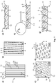
- Fig. 1 shows, with a schematic series of pictures, the main and partially sectioned method stages according to an inventive method of a first embodiment.
- the method serves to produce an inventive electrically conductive contact element 1 according to an exemplary embodiment.
- the contact element 1 for an electrical connector 3 has a contact surface 5.
- Caverns 7 filled with an auxiliary material 9 are located under the contact surface 5.
- the caverns 7 are arranged under the contact surface 5 in a microstructure 11.
- the caverns 7 in the microstructure 11 are spaced regularly at a spacing a from one another in the microstructure 11.
- the spacing is at 0.5 to 300 ⁇ m, for example.
- the starting material of the method according to the invention is a contact element 1 of a connector 3.
- the contact element 1 is electrically conductive and consists of a base material 13.
- the base material 13 can be copper or a copper alloy, for example.
- a microstructure 11 is produced at the contact surface 5 of the base material 13 ( Fig. 1A and 1C ).
- the microstructure 11 consists of, for example, elevations 15 and recesses 17 which periodically alternate with one another.
- the recesses 17 form, in the example of Fig. 1A , trenches 23, and the elevations form walls between them.
- Two adjacent recesses 17 have a spacing a of 0.5 to 300 ⁇ m, depending on the production method. In this way, a regular, periodic stripe structure arises as the microstructure 11 with a period length p which corresponds to the spacing a in the microstructure 11.
- FIG. 1C an alternative microstructure 11 is shown in a schematic top view.
- the microstructure 11 in Fig. 1C also has a homogenous pattern 19 with periodic elevations 15 and recesses 17, wherein the recesses are formed substantially as circular disk-shaped holes 21.
- two adjacent holes 21 have a spacing a of, for example, 0.5 to 300 ⁇ m, which corresponds to that of the period length p.
- the microstructure 11 at the contact surface 5 which is shown in Fig. 1A or 1C can be created, for example, with the help of a laser or an electron beam.
- very large contact surfaces can be microstructured in a short period of time by using a laser or electron beam.
- other surface treatments for example masking and etching, can be employed to form the microstructure 11.
- the application of the auxiliary material 9 onto the contact surface 5 takes place in a next step according to the exemplary method of Fig. 1 .
- the auxiliary material 9 is filled into the recesses 17, i.e. the trenches 23 or holes 21 of the microstructure 11.
- auxiliary material 9 is enclosed in the microstructure 11.
- the surface 5 is mechanically deformed, e.g. rolled, to enclose the auxiliary material 9.
- the auxiliary materials 9 are enclosed in the microstructure 11, since the areas of the microstructure 11 with elevations 15 are rolled over the auxiliary material 9 arranged in the recesses 17.
- the recesses 17 are sealed and caverns 7 filled with auxiliary material 9 are formed.
- the electrically conductive contact element 1 for an electrical connector 3 which results therefrom is schematically illustrated in Fig. 1G , in which the caverns 7 filled with an auxiliary material 9, which are arranged in a microstructure 11 in the contact surface 5, can be identified.
- the auxiliary material 9 could also be enclosed in the microstructure 11 by administering a sealant (not shown) onto the surface 5 of the intermediate step shown in Fig. 1E .
- a coating (not shown) could be deposited onto the surface 5 in the intermediate step shown in Fig. 1E in order to seal the recesses 17 to enclose the auxiliary material 9 in the caverns 7.
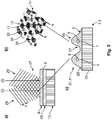
- a further exemplary method according to the invention for enclosing an auxiliary material 9 under the contact surface 5 of an electrically conductive contact element 1 for a connector 3 is shown.
- the contact element 1 for the connector 3 in turn comprises a base material 13.
- the base material 13, as in the embodiment of Fig. 1 can be copper or a copper alloy, for example.
- a coating 25 is arranged on a surface of the base material 13.
- the coating 25 can have, for example, tin, nickel, silver or alloys of tin, nickel, silver and/or other elements.
- the coating 25 can be applied onto the base material 13 by hot-dip tinning, for example. A surface of the coating 25 facing away from the base material forms the contact surface 5.
- the auxiliary material 9 is firstly applied onto the contact surface 5.
- the contact surface 5 can, for example, be completely coated with the auxiliary material 9, as illustrated in Fig. 2A , for example.
- the auxiliary material 9 can have, for example, oil, grease, a paste or a solid lubricant such as graphite, CNT, MoS2, AgS2 or a combination thereof.
- the auxiliary material 9 After the auxiliary material 9 has been applied onto the contact surface 5, the microstructure 11 is subsequently formed.
- the auxiliary material 9 is enclosed in the microstructure 11 when forming the microstructure 11.
- the contact surface is treated with an interference pattern 27 by laser radiation 29, 29'.
- two or more overlapping, preferably coherently or linearly polarising laser beams 29, 29' produce a systematically adjustable interference pattern 27.
- a prerequisite for this is the spatial and temporal coherence of the laser radiation 29, 29'.
- the spatial coherence can be compromised by interaction with the environment or the optical elements of the apparatus for creating the interference radiation.
- the temporal coherence depends on the spectral bandwidth ⁇ of the laser radiation 29, 29'. Standard coherence lengths of the spectral bandwidth are in the range of 266 to 1064 nm.
- interference patterns 27 for example line patterns, dot patterns, honeycomb patterns, cross-shaped patterns, etc. can thus be created.
- the interference pattern 27 gives the microstructure 11 and the surface textures 31 of the contact surface 5.
- the contact surface S is treated with an interference pattern 27 of laser radiation 29, 29', two or more overlapping, coherent and linearly polarising laser beams 29, 29' produce a systematically adjustable interference pattern 27.
- the intensity of the laser radiation is distributed within the interference pattern 27.
- positive interference (+) it intensifies and leads to particularly hot areas at which the contact surface 5 melts.
- negative interference (-) at the minimum intensity, the contact surface 5 is much colder, such that the contact surface 5 does not melt or rather auxiliary material 9 at this location is still present, whereas it is vaporised in regions of positive interference.
- molten material of the contact surface 5 is convected and a texture 31 develops.
- the texture 31 develops in that material of the contact surface 5 is directed from areas of a maximum temperature and transported to areas of a minimum temperature.
- a contact surface 5 of an electrically conductive contact element 1, onto which a layer of auxiliary material 9 has been applied is irradiated with an interference pattern 27 of laser radiation 29, 29' ( Fig. 1A )
- the material melts the contact surface 5 in areas of positive interference and spills, in a directed manner, into the areas of negative interference where, forming elevations 15, it covers the auxiliary material 9 which remains there.
- a contact surface 5, such as in Fig. 2B and 2C can be formed which has a burl structure 33, wherein every burl 33 has a cavity 7 filled with auxiliary substances.
- the auxiliary material 9 is thus enclosed in the microstructure 11 when forming the microstructure 11.
- a texturing 31 of the contact surface 5 takes place.
- the surface texture 31 is formed by a burl structure 33 with regularly arranged burls 35 and recesses 17 in between.
- the surface texture 31, i.e. the burl structure 33 is congruent with the microstructure 11 of the caverns 7 filled with auxiliary materials 9.
- the surface texture 31 is elevated above a cavern 7 of the microstructure 11.
- a cavern 7 filled with auxiliary materials 9 is arranged in every burl 35.
- FIG. 3 shows a highly schematic and partially sectioned illustration of portions of a connector 3 with an electrically conductive contact element 1 according to the invention with a mating connector 37 while being plugged together.
- Fig. 3 shows a contact element 1 of the connector.
- the contact element 1 is formed, for example, as a contact pin and is illustrated as sectioned.
- the contact element 1 is electrically conductive and consists of a base material 13, for example a copper or copper alloy.
- the contact element 1 has a contact surface 5.
- Caverns 7 filled with auxiliary material 9 are arranged under the contact surface 5 in a microstructure 11.
- the contact surface 5 in the shown embodiment has a surface texture 31 which consists of periodically alternating elevations 15 and recesses 17.
- a cavern 7, which is filled with auxiliary material 9, of the microstructure 11 is arranged in every elevation 15.
- the surface texture 31 and the microstructure 11 of the contact element 1 of Fig. 3 thus correspond substantially to those of Fig. 2 , with the exception that the coating 25 has been omitted and the auxiliary material 9 has been administered directly onto the base material 13.
- Fig. 3 further shows a portion of a further contact element 39 of a mating connector 37.
- the mating connector 37 is intended to be plugged together with the connector 3.
- the further contact element 39 has a further contact surface 41 which comes into contact with the contact surface 5 of the contact element 1 when the connector 3 is plugged together with the mating connector 37.
- the further contact element 39 is formed as an elastically deformable contact spring.
- the further contact element 39 touches the contact element 1 in order to produce an electrically conductive connection. While the connector 3 is being plugged together with the mating connector 37, the contact element 1 moves along a relative plugging direction 43 relative to the further contact element 39.
- the contact surface 5 Due to the pressing force exerted by the contact surface 41 of the further contact element 39 onto the contact surface 5 of the contact element 1, frictional forces act between contact surface 5 and the further contact surface 41, which must be overcome while the connector 3 is being plugged together with the mating connector 37.
- the contact surface 5 is equipped with a surface texture 31. Furthermore, the surface texture 31 and the microstructure 11 of the contact element 1 are partially broken open while being plugged together. Entrances to the closed caverns 7, which were previously under the contact surface 5, are created by the frictional forces. The caverns 7 open out onto the contact surface 5.
- the auxiliary material 9 can emerge from the cavern 7 and form a film 45 of auxiliary material 9 on the contact surface 5, which forms the desired positive effect, for example reducing friction, corrosion protection.
Landscapes
- Engineering & Computer Science (AREA)
- Chemical & Material Sciences (AREA)
- Manufacturing & Machinery (AREA)
- Materials Engineering (AREA)
- Mechanical Engineering (AREA)
- Metallurgy (AREA)
- Organic Chemistry (AREA)
- Manufacturing Of Electrical Connectors (AREA)
- Coupling Device And Connection With Printed Circuit (AREA)
Claims (15)
- Elektrisch leitendes Kontaktelement (1) für einen elektrischen Verbinder (3), das eine Kontaktfläche (5) aufweist, wobei mit einem Hilfsmaterial (9) gefüllte Hohlräume (7) unter der Kontaktfläche (5) in eine Mikrogefüge (11) angeordnet sind, dadurch gekennzeichnet, dass die Kontaktfläche (5) eine Oberflächentextur (31) mit einem deterministischen Muster geometrischer Elemente aufweist.
- Elektrisch leitendes Kontaktelement (1) nach Anspruch 1, dadurch gekennzeichnet, dass sich das Mikrogefüge (11) parallel zu der Kontaktfläche (5) erstreckt.
- Elektrisch leitendes Kontaktelement nach Anspruch 1 oder 2, dadurch gekennzeichnet, dass die Hohlräume (7) mit dem Mikrogefüge (11) ein im Wesentlichen homogenes Muster (19) bilden.
- Elektrisch leitendes Kontaktelement (1) nach einem der Ansprüche 1 bis 3, dadurch gekennzeichnet, dass das Mikrogefüge (11) eine Struktur bildet, die wenigstens in Abschnitten periodisch ist.
- Elektrisch leitendes Kontaktelement (1) nach Anspruch 4, dadurch gekennzeichnet, dass das periodische Mikrogefüge (11) in wenigstens einer Richtung eine Periodenlänge (p) von 0,5 µm bis 300 µm, vorzugsweise von 1 µm bis 100 µm, hat.
- Elektrisch leitendes Kontaktelement (1) nach einem der Ansprüche 1 bis 5, dadurch gekennzeichnet, dass das Hilfsmaterial (9) aus der Gruppe von Antioxidantien, Korrosionsschutzmitteln, Schmiermitteln und Säuren ausgewählt wird.
- Elektrisch leitendes Kontaktelement (1) nach einem der Ansprüche 1 bis 6, dadurch gekennzeichnet, dass die Oberflächentextur (31) im Wesentlichen kongruent mit dem Mikrogefüge (11) der Hohlräume (7) ist.
- Elektrisch leitendes Kontaktelement (1) nach einem der Ansprüche 1 bis 7, dadurch gekennzeichnet, dass die Oberflächentextur (31) über einen Hohlraum (7) des Mikrogefüges (11) erhöht ist.
- Elektrischer Verbinder (3), umfassend ein elektrisch leitendes Kontaktelement (1) nach einem der Ansprüche 1 bis 8.
- Verfahren zum Einschließen eines Hilfsmaterials (9) unter der Kontaktfläche (5) eines elektrisch leitenden Kontaktelementes (1) für einen elektrischen Verbinder (3), umfassend die folgenden Schritte:- Ausbilden eines Mikrogefüges (11) an der Kontaktfläche (5),- Aufbringen des Hilfsmaterials (9) auf die Kontaktfläche (5),- Einschließen des Hilfsmaterials (9) in das Mikrogefüge (11), so dass mit dem Hilfsmaterial (9) gefüllte Hohlräume (7) unter der Kontaktfläche angeordnet sind, gekennzeichnet durch Entwickeln einer Oberflächentextur (31) mit einem deterministischen Muster geometrischer Elemente an der Kontaktfläche (5).
- Verfahren nach Anspruch 10, dadurch gekennzeichnet, dass zunächst das Hilfsmaterial (9) auf die Kontaktfläche (5) aufgebracht wird und anschließend das Mikrogefüge (11) ausgebildet wird.
- Verfahren nach Anspruch 11, dadurch gekennzeichnet, dass das Hilfsmaterial (9) beim Ausbilden des Mikrogefüges (11) in den Hohlräumen (7) des Mikrogefüges (11) eingeschlossen wird.
- Verfahren nach Anspruch 10, dadurch gekennzeichnet, dass das Hilfsmaterial (9) im Anschluss an den Schritt zum Ausbilden in die Mikrostruktur (11) eingebracht wird.
- Verfahren nach Anspruch 13, dadurch gekennzeichnet, dass die Kontaktfläche (5) mechanisch verformt wird, um das Hilfsmaterial (9) einzuschließen, oder eine Dichtung auf die Kontaktfläche (5) aufgebracht wird.
- Verfahren nach einem der Ansprüche 10 bis 14, dadurch gekennzeichnet, dass die Kontaktfläche (5) mit Laserstrahlung (29), vorzugsweise mit einem Interferenzmuster (27) aus Laserstrahlung (29, 29'), behandelt wird, um das Mikrogefüge (11) auszubilden.
Applications Claiming Priority (2)
| Application Number | Priority Date | Filing Date | Title |
|---|---|---|---|
| DE102016214693.9A DE102016214693B4 (de) | 2016-08-08 | 2016-08-08 | Elektrisch leitendes Kontaktelement für einen elektrischen Steckverbinder, elektrischer Steckverbinder, der ein solches Kontaktelement umfasst, und Verfahren zum Einschließen eines Hilfsstoffes unter der Kontaktoberfläche eines solchen Kontaktelements |
| PCT/EP2017/070037 WO2018029179A1 (en) | 2016-08-08 | 2017-08-08 | Electrical contact element for an electrical connector having microstructured caverns under the contact surface |
Publications (2)
| Publication Number | Publication Date |
|---|---|
| EP3497752A1 EP3497752A1 (de) | 2019-06-19 |
| EP3497752B1 true EP3497752B1 (de) | 2021-02-17 |
Family
ID=59683520
Family Applications (1)
| Application Number | Title | Priority Date | Filing Date |
|---|---|---|---|
| EP17755097.7A Active EP3497752B1 (de) | 2016-08-08 | 2017-08-08 | Elektrisches kontaktelement für einen elektrischen verbinder mit mikrostrukturierten hohlräumen unter der kontaktfläche |
Country Status (7)
| Country | Link |
|---|---|
| US (1) | US11239593B2 (de) |
| EP (1) | EP3497752B1 (de) |
| JP (1) | JP6759449B2 (de) |
| CN (1) | CN110870142B (de) |
| DE (1) | DE102016214693B4 (de) |
| TW (1) | TWI786056B (de) |
| WO (1) | WO2018029179A1 (de) |
Families Citing this family (7)
| Publication number | Priority date | Publication date | Assignee | Title |
|---|---|---|---|---|
| DE102020118434B4 (de) | 2020-07-13 | 2024-10-31 | Amphenol-Tuchel Electronics Gmbh | Elektrisches Kontaktelement und dessen Herstellungsverfahren |
| DE102020134045B3 (de) | 2020-12-17 | 2022-05-12 | Te Connectivity Germany Gmbh | Schmierstoffapplikator und Verfahren zum Auftragen eines Festschmierstoffes sowie Applikatorvorrichtung, Anordnung und Ladestation |
| DE102021122892A1 (de) * | 2021-09-03 | 2023-03-09 | Te Connectivity Germany Gmbh | Mit einem Fenster zum Laserschweißen versehenes Halbfabrikat zur Herstellung eines elektrischen Kontaktelements sowie Verfahren zur Herstellung eines elektrischen Kontaktelements und elektrisches Kontaktelement |
| DE202021104874U1 (de) | 2021-09-09 | 2022-12-12 | Reinz-Dichtungs-Gmbh | Platte für ein elektrochemisches, medienführendes System, Kontaktelement und Übertragungseinrichtung |
| DE102021130188A1 (de) * | 2021-11-18 | 2023-05-25 | Te Connectivity Germany Gmbh | Verfahren zur oberflächenbehandlung eines elektrischen kontaktlements und kontaktelement |
| EP4187723A1 (de) | 2021-11-25 | 2023-05-31 | Tyco Electronics France SAS | Elektrisch leitendes kontaktelement für einen steckverbinder |
| DE102023106086A1 (de) * | 2023-03-10 | 2024-09-12 | Te Connectivity Solutions Gmbh | Elektrisches kontaktelement für einen elektrischen steckverbinder mit oberflächentextur und verfahren zur oberflächenbehandlung eines elektrischen kontaktelementes |
Family Cites Families (29)
| Publication number | Priority date | Publication date | Assignee | Title |
|---|---|---|---|---|
| US3648002A (en) * | 1970-05-04 | 1972-03-07 | Essex International Inc | Current control apparatus and methods of manufacture |
| US4328410A (en) * | 1978-08-24 | 1982-05-04 | Slivinsky Sandra H | Laser skiving system |
| JP3650546B2 (ja) * | 1998-08-28 | 2005-05-18 | 松下電器産業株式会社 | 導電性ペースト、およびそれを用いた導電性構造、セラミック電子部品、電子部品、実装体、回路基板、電気的接続方法、回路基板の製造方法、及びセラミック電子部品の製造方法 |
| JP2002343168A (ja) * | 2001-05-11 | 2002-11-29 | Mitsubishi Electric Corp | 摺動通電体 |
| DE10146274A1 (de) * | 2001-09-19 | 2003-04-10 | Bosch Gmbh Robert | Metallische Oberfläche eines Körpers, Verfahren zur Herstellung einer strukturierten metallischen Oberfläche eines Körpers und dessen Verwendung |
| DE10224693A1 (de) | 2002-06-04 | 2003-12-18 | Bosch Gmbh Robert | Verbundwerkstoff zur Herstellung einer elektrischen Kontaktfläche sowie Verfahren zur Erzeugung einer gleitfähigen und korrosionsarmen elektrischen Kontaktoberfläche |
| DE10245343A1 (de) * | 2002-09-27 | 2004-04-08 | Robert Bosch Gmbh | Elektrischer Kontakt |
| JP4112426B2 (ja) * | 2003-05-14 | 2008-07-02 | 三菱伸銅株式会社 | めっき処理材の製造方法 |
| DE10326788B4 (de) * | 2003-06-13 | 2005-05-25 | Robert Bosch Gmbh | Kontaktoberflächen für elektrische Kontakte und Verfahren zur Herstellung |
| WO2007118337A1 (en) | 2006-04-13 | 2007-10-25 | Abb Research Ltd | Electrical contact assembly |
| JP4729064B2 (ja) * | 2007-04-03 | 2011-07-20 | 古河電気工業株式会社 | 電気接点材料、その製造方法、及び電気接点 |
| DE102008030988B4 (de) * | 2008-06-27 | 2010-04-01 | Siemens Aktiengesellschaft | Bauteil mit einer Schicht, in die CNT (Carbon Nanotubes) eingebaut sind und Verfahren zu dessen Herstellung |
| EP2144231A1 (de) | 2008-07-11 | 2010-01-13 | Fraunhofer-Gesellschaft zur Förderung der angewandten Forschung e.V. | Audiokodierungs-/-dekodierungschema geringer Bitrate mit gemeinsamer Vorverarbeitung |
| DE102009036311B4 (de) | 2009-08-06 | 2021-10-28 | Te Connectivity Corporation | Selbstschmierende Beschichtung, selbstschmierendes Bauteil, Beschichtungselektrolyt und Verfahren zur Herstellung einer selbstschmierenden Beschichtung |
| JP2012057212A (ja) * | 2010-09-08 | 2012-03-22 | Furukawa Electric Co Ltd:The | 複合めっき材料、及びそのめっき材料を用いた電気・電子部品 |
| JP5260620B2 (ja) * | 2010-12-07 | 2013-08-14 | 株式会社神戸製鋼所 | Pcb端子及びその製造方法 |
| JP2012142152A (ja) | 2010-12-28 | 2012-07-26 | Tyco Electronics Japan Kk | 回路基板組立体、基板装置、回路基板組立体の組み立て方法 |
| EP2528167B1 (de) | 2011-05-25 | 2014-04-30 | Tyco Electronics AMP GmbH | Elektrisches Kontaktelement mit einer Deckschicht mit chemischem Reduktionsmittel, elektrische Kontaktanordnung und Verfahren zur Herstellung eines elektrischen Kontaktelements und zur Reduktion der Oxidierung eines Kontaktabschnitts eines elektrischen Kontaktelements |
| KR20140036293A (ko) | 2011-06-03 | 2014-03-25 | 파나소닉 주식회사 | 전기 접점 부품 |
| US9634412B2 (en) * | 2011-07-15 | 2017-04-25 | Tessera, Inc. | Connector structures and methods |
| JP5724736B2 (ja) | 2011-08-09 | 2015-05-27 | 住友電装株式会社 | コネクタ |
| WO2013074038A1 (en) | 2011-11-17 | 2013-05-23 | Andre Benny | Electrical contact with embedded solid lubricant particles |
| DE102011088793A1 (de) * | 2011-12-16 | 2013-06-20 | Tyco Electronics Amp Gmbh | Elektrischer Steckverbinder mit mikrostrukturiertem Kontaktelement |
| CN102701109B (zh) * | 2012-06-29 | 2014-04-16 | 烟台三重技术开发有限公司 | 一种汽车车体校正机的单缸柔性举升机构 |
| JP5692192B2 (ja) * | 2012-09-21 | 2015-04-01 | 株式会社オートネットワーク技術研究所 | コネクタ端子の製造方法およびコネクタ端子用材料の製造方法 |
| DE102012112550A1 (de) * | 2012-12-18 | 2014-06-18 | Lpkf Laser & Electronics Ag | Verfahren zur Metallisierung eines Werkstücks sowie ein Schichtaufbau aus einem Werkstück und einer Metallschicht |
| TWI557750B (zh) * | 2014-02-05 | 2016-11-11 | Furukawa Electric Co Ltd | Electrical contact material and manufacturing method thereof |
| US20160344127A1 (en) * | 2015-05-20 | 2016-11-24 | Delphi Technologies, Inc. | Electroconductive material with an undulating surface, an electrical terminal formed of said material, and a method of producing said material |
| US20170012377A1 (en) * | 2015-07-09 | 2017-01-12 | Denso Corporation | Electrical component and electronic device |
-
2016
- 2016-08-08 DE DE102016214693.9A patent/DE102016214693B4/de not_active Expired - Fee Related
-
2017
- 2017-08-08 TW TW106126754A patent/TWI786056B/zh active
- 2017-08-08 EP EP17755097.7A patent/EP3497752B1/de active Active
- 2017-08-08 JP JP2019506668A patent/JP6759449B2/ja active Active
- 2017-08-08 WO PCT/EP2017/070037 patent/WO2018029179A1/en not_active Ceased
- 2017-08-08 CN CN201780048826.7A patent/CN110870142B/zh active Active
-
2019
- 2019-02-08 US US16/270,716 patent/US11239593B2/en active Active
Non-Patent Citations (1)
| Title |
|---|
| None * |
Also Published As
| Publication number | Publication date |
|---|---|
| US11239593B2 (en) | 2022-02-01 |
| WO2018029179A1 (en) | 2018-02-15 |
| DE102016214693A1 (de) | 2018-02-08 |
| US20190173214A1 (en) | 2019-06-06 |
| EP3497752A1 (de) | 2019-06-19 |
| JP6759449B2 (ja) | 2020-09-23 |
| TW201820712A (zh) | 2018-06-01 |
| DE102016214693B4 (de) | 2018-05-09 |
| JP2019525421A (ja) | 2019-09-05 |
| CN110870142B (zh) | 2022-07-12 |
| TWI786056B (zh) | 2022-12-11 |
| CN110870142A (zh) | 2020-03-06 |
Similar Documents
| Publication | Publication Date | Title |
|---|---|---|
| WO2018029179A1 (en) | Electrical contact element for an electrical connector having microstructured caverns under the contact surface | |
| EP2792028B1 (de) | Elektrischer steckverbinder mit einem mikrostrukturierten kontaktelement | |
| US9061593B2 (en) | Sliding strip for a sliding contact device and method for producing a sliding strip | |
| WO2016187089A1 (en) | An electroconductive material with an undulating surface, an electrical terminal formed of said material, and a method of producing said material | |
| CN106207500B (zh) | 具有精细结构的接触表面的电接触元件 | |
| US20130014979A1 (en) | Connector Structures and Methods | |
| EP3533116A1 (de) | Gleitringmodul | |
| EP4429033A1 (de) | Elektrisches kontaktelement für einen elektrischen verbinder mit oberflächentextur und verfahren zur oberflächenbehandlung eines elektrischen kontaktelements | |
| CN116136021B (zh) | 电接触元件的表面处理方法及接触元件 | |
| KR102926942B1 (ko) | 스프레이 코팅을 갖는 접촉 요소 뿐만 아니라 연결 조립체, 스프레이 매체의 용도, 및 접촉 요소를 제조하기 위한 방법 | |
| US7968141B2 (en) | Method for producing contact terminal with textured surface and use thereof | |
| RU2768808C1 (ru) | СПОСОБ НАНЕСЕНИЯ ЭЛЕКТРОЭРОЗИОННОСТОЙКИХ ПОКРЫТИЙ СИСТЕМЫ Mo-C-Ag-N НА МЕДНЫЕ ЭЛЕКТРИЧЕСКИЕ КОНТАКТЫ | |
| RU2699486C1 (ru) | Способ нанесения электроэрозионностойких покрытий на основе оксида меди и серебра на медные электрические контакты | |
| KR100999674B1 (ko) | 커넥터 단자용 압연판 및 그 제조방법 | |
| Leidner et al. | Experimental verification/comparison between standard sphere against flat and a new wave structured contact surface topography developed using a numerical contact model; as applied to an existing MQS contact design |
Legal Events
| Date | Code | Title | Description |
|---|---|---|---|
| STAA | Information on the status of an ep patent application or granted ep patent |
Free format text: STATUS: UNKNOWN |
|
| STAA | Information on the status of an ep patent application or granted ep patent |
Free format text: STATUS: THE INTERNATIONAL PUBLICATION HAS BEEN MADE |
|
| PUAI | Public reference made under article 153(3) epc to a published international application that has entered the european phase |
Free format text: ORIGINAL CODE: 0009012 |
|
| STAA | Information on the status of an ep patent application or granted ep patent |
Free format text: STATUS: REQUEST FOR EXAMINATION WAS MADE |
|
| 17P | Request for examination filed |
Effective date: 20190307 |
|
| AK | Designated contracting states |
Kind code of ref document: A1 Designated state(s): AL AT BE BG CH CY CZ DE DK EE ES FI FR GB GR HR HU IE IS IT LI LT LU LV MC MK MT NL NO PL PT RO RS SE SI SK SM TR |
|
| AX | Request for extension of the european patent |
Extension state: BA ME |
|
| DAV | Request for validation of the european patent (deleted) | ||
| DAX | Request for extension of the european patent (deleted) | ||
| GRAP | Despatch of communication of intention to grant a patent |
Free format text: ORIGINAL CODE: EPIDOSNIGR1 |
|
| STAA | Information on the status of an ep patent application or granted ep patent |
Free format text: STATUS: GRANT OF PATENT IS INTENDED |
|
| INTG | Intention to grant announced |
Effective date: 20200520 |
|
| GRAJ | Information related to disapproval of communication of intention to grant by the applicant or resumption of examination proceedings by the epo deleted |
Free format text: ORIGINAL CODE: EPIDOSDIGR1 |
|
| STAA | Information on the status of an ep patent application or granted ep patent |
Free format text: STATUS: REQUEST FOR EXAMINATION WAS MADE |
|
| GRAP | Despatch of communication of intention to grant a patent |
Free format text: ORIGINAL CODE: EPIDOSNIGR1 |
|
| STAA | Information on the status of an ep patent application or granted ep patent |
Free format text: STATUS: GRANT OF PATENT IS INTENDED |
|
| INTC | Intention to grant announced (deleted) | ||
| INTG | Intention to grant announced |
Effective date: 20200928 |
|
| GRAS | Grant fee paid |
Free format text: ORIGINAL CODE: EPIDOSNIGR3 |
|
| GRAA | (expected) grant |
Free format text: ORIGINAL CODE: 0009210 |
|
| STAA | Information on the status of an ep patent application or granted ep patent |
Free format text: STATUS: THE PATENT HAS BEEN GRANTED |
|
| AK | Designated contracting states |
Kind code of ref document: B1 Designated state(s): AL AT BE BG CH CY CZ DE DK EE ES FI FR GB GR HR HU IE IS IT LI LT LU LV MC MK MT NL NO PL PT RO RS SE SI SK SM TR |
|
| REG | Reference to a national code |
Ref country code: GB Ref legal event code: FG4D |
|
| REG | Reference to a national code |
Ref country code: CH Ref legal event code: EP |
|
| REG | Reference to a national code |
Ref country code: DE Ref legal event code: R096 Ref document number: 602017032733 Country of ref document: DE |
|
| REG | Reference to a national code |
Ref country code: AT Ref legal event code: REF Ref document number: 1362701 Country of ref document: AT Kind code of ref document: T Effective date: 20210315 |
|
| REG | Reference to a national code |
Ref country code: IE Ref legal event code: FG4D |
|
| REG | Reference to a national code |
Ref country code: LT Ref legal event code: MG9D |
|
| REG | Reference to a national code |
Ref country code: NL Ref legal event code: MP Effective date: 20210217 |
|
| PG25 | Lapsed in a contracting state [announced via postgrant information from national office to epo] |
Ref country code: BG Free format text: LAPSE BECAUSE OF FAILURE TO SUBMIT A TRANSLATION OF THE DESCRIPTION OR TO PAY THE FEE WITHIN THE PRESCRIBED TIME-LIMIT Effective date: 20210517 Ref country code: LT Free format text: LAPSE BECAUSE OF FAILURE TO SUBMIT A TRANSLATION OF THE DESCRIPTION OR TO PAY THE FEE WITHIN THE PRESCRIBED TIME-LIMIT Effective date: 20210217 Ref country code: HR Free format text: LAPSE BECAUSE OF FAILURE TO SUBMIT A TRANSLATION OF THE DESCRIPTION OR TO PAY THE FEE WITHIN THE PRESCRIBED TIME-LIMIT Effective date: 20210217 Ref country code: FI Free format text: LAPSE BECAUSE OF FAILURE TO SUBMIT A TRANSLATION OF THE DESCRIPTION OR TO PAY THE FEE WITHIN THE PRESCRIBED TIME-LIMIT Effective date: 20210217 Ref country code: GR Free format text: LAPSE BECAUSE OF FAILURE TO SUBMIT A TRANSLATION OF THE DESCRIPTION OR TO PAY THE FEE WITHIN THE PRESCRIBED TIME-LIMIT Effective date: 20210518 Ref country code: NO Free format text: LAPSE BECAUSE OF FAILURE TO SUBMIT A TRANSLATION OF THE DESCRIPTION OR TO PAY THE FEE WITHIN THE PRESCRIBED TIME-LIMIT Effective date: 20210517 Ref country code: PT Free format text: LAPSE BECAUSE OF FAILURE TO SUBMIT A TRANSLATION OF THE DESCRIPTION OR TO PAY THE FEE WITHIN THE PRESCRIBED TIME-LIMIT Effective date: 20210617 |
|
| REG | Reference to a national code |
Ref country code: AT Ref legal event code: MK05 Ref document number: 1362701 Country of ref document: AT Kind code of ref document: T Effective date: 20210217 |
|
| PG25 | Lapsed in a contracting state [announced via postgrant information from national office to epo] |
Ref country code: SE Free format text: LAPSE BECAUSE OF FAILURE TO SUBMIT A TRANSLATION OF THE DESCRIPTION OR TO PAY THE FEE WITHIN THE PRESCRIBED TIME-LIMIT Effective date: 20210217 Ref country code: NL Free format text: LAPSE BECAUSE OF FAILURE TO SUBMIT A TRANSLATION OF THE DESCRIPTION OR TO PAY THE FEE WITHIN THE PRESCRIBED TIME-LIMIT Effective date: 20210217 Ref country code: LV Free format text: LAPSE BECAUSE OF FAILURE TO SUBMIT A TRANSLATION OF THE DESCRIPTION OR TO PAY THE FEE WITHIN THE PRESCRIBED TIME-LIMIT Effective date: 20210217 Ref country code: PL Free format text: LAPSE BECAUSE OF FAILURE TO SUBMIT A TRANSLATION OF THE DESCRIPTION OR TO PAY THE FEE WITHIN THE PRESCRIBED TIME-LIMIT Effective date: 20210217 Ref country code: RS Free format text: LAPSE BECAUSE OF FAILURE TO SUBMIT A TRANSLATION OF THE DESCRIPTION OR TO PAY THE FEE WITHIN THE PRESCRIBED TIME-LIMIT Effective date: 20210217 |
|
| PG25 | Lapsed in a contracting state [announced via postgrant information from national office to epo] |
Ref country code: IS Free format text: LAPSE BECAUSE OF FAILURE TO SUBMIT A TRANSLATION OF THE DESCRIPTION OR TO PAY THE FEE WITHIN THE PRESCRIBED TIME-LIMIT Effective date: 20210617 |
|
| PG25 | Lapsed in a contracting state [announced via postgrant information from national office to epo] |
Ref country code: CZ Free format text: LAPSE BECAUSE OF FAILURE TO SUBMIT A TRANSLATION OF THE DESCRIPTION OR TO PAY THE FEE WITHIN THE PRESCRIBED TIME-LIMIT Effective date: 20210217 Ref country code: EE Free format text: LAPSE BECAUSE OF FAILURE TO SUBMIT A TRANSLATION OF THE DESCRIPTION OR TO PAY THE FEE WITHIN THE PRESCRIBED TIME-LIMIT Effective date: 20210217 Ref country code: AT Free format text: LAPSE BECAUSE OF FAILURE TO SUBMIT A TRANSLATION OF THE DESCRIPTION OR TO PAY THE FEE WITHIN THE PRESCRIBED TIME-LIMIT Effective date: 20210217 Ref country code: SM Free format text: LAPSE BECAUSE OF FAILURE TO SUBMIT A TRANSLATION OF THE DESCRIPTION OR TO PAY THE FEE WITHIN THE PRESCRIBED TIME-LIMIT Effective date: 20210217 |
|
| REG | Reference to a national code |
Ref country code: DE Ref legal event code: R097 Ref document number: 602017032733 Country of ref document: DE |
|
| PG25 | Lapsed in a contracting state [announced via postgrant information from national office to epo] |
Ref country code: RO Free format text: LAPSE BECAUSE OF FAILURE TO SUBMIT A TRANSLATION OF THE DESCRIPTION OR TO PAY THE FEE WITHIN THE PRESCRIBED TIME-LIMIT Effective date: 20210217 Ref country code: DK Free format text: LAPSE BECAUSE OF FAILURE TO SUBMIT A TRANSLATION OF THE DESCRIPTION OR TO PAY THE FEE WITHIN THE PRESCRIBED TIME-LIMIT Effective date: 20210217 Ref country code: SK Free format text: LAPSE BECAUSE OF FAILURE TO SUBMIT A TRANSLATION OF THE DESCRIPTION OR TO PAY THE FEE WITHIN THE PRESCRIBED TIME-LIMIT Effective date: 20210217 |
|
| PLBE | No opposition filed within time limit |
Free format text: ORIGINAL CODE: 0009261 |
|
| STAA | Information on the status of an ep patent application or granted ep patent |
Free format text: STATUS: NO OPPOSITION FILED WITHIN TIME LIMIT |
|
| 26N | No opposition filed |
Effective date: 20211118 |
|
| PG25 | Lapsed in a contracting state [announced via postgrant information from national office to epo] |
Ref country code: AL Free format text: LAPSE BECAUSE OF FAILURE TO SUBMIT A TRANSLATION OF THE DESCRIPTION OR TO PAY THE FEE WITHIN THE PRESCRIBED TIME-LIMIT Effective date: 20210217 Ref country code: ES Free format text: LAPSE BECAUSE OF FAILURE TO SUBMIT A TRANSLATION OF THE DESCRIPTION OR TO PAY THE FEE WITHIN THE PRESCRIBED TIME-LIMIT Effective date: 20210217 |
|
| PG25 | Lapsed in a contracting state [announced via postgrant information from national office to epo] |
Ref country code: SI Free format text: LAPSE BECAUSE OF FAILURE TO SUBMIT A TRANSLATION OF THE DESCRIPTION OR TO PAY THE FEE WITHIN THE PRESCRIBED TIME-LIMIT Effective date: 20210217 |
|
| REG | Reference to a national code |
Ref country code: CH Ref legal event code: PL |
|
| PG25 | Lapsed in a contracting state [announced via postgrant information from national office to epo] |
Ref country code: MC Free format text: LAPSE BECAUSE OF FAILURE TO SUBMIT A TRANSLATION OF THE DESCRIPTION OR TO PAY THE FEE WITHIN THE PRESCRIBED TIME-LIMIT Effective date: 20210217 |
|
| REG | Reference to a national code |
Ref country code: BE Ref legal event code: MM Effective date: 20210831 |
|
| GBPC | Gb: european patent ceased through non-payment of renewal fee |
Effective date: 20210808 |
|
| PG25 | Lapsed in a contracting state [announced via postgrant information from national office to epo] |
Ref country code: LI Free format text: LAPSE BECAUSE OF NON-PAYMENT OF DUE FEES Effective date: 20210831 Ref country code: CH Free format text: LAPSE BECAUSE OF NON-PAYMENT OF DUE FEES Effective date: 20210831 |
|
| PG25 | Lapsed in a contracting state [announced via postgrant information from national office to epo] |
Ref country code: IS Free format text: LAPSE BECAUSE OF FAILURE TO SUBMIT A TRANSLATION OF THE DESCRIPTION OR TO PAY THE FEE WITHIN THE PRESCRIBED TIME-LIMIT Effective date: 20210617 Ref country code: LU Free format text: LAPSE BECAUSE OF NON-PAYMENT OF DUE FEES Effective date: 20210808 |
|
| PG25 | Lapsed in a contracting state [announced via postgrant information from national office to epo] |
Ref country code: IE Free format text: LAPSE BECAUSE OF NON-PAYMENT OF DUE FEES Effective date: 20210808 Ref country code: GB Free format text: LAPSE BECAUSE OF NON-PAYMENT OF DUE FEES Effective date: 20210808 Ref country code: BE Free format text: LAPSE BECAUSE OF NON-PAYMENT OF DUE FEES Effective date: 20210831 |
|
| PG25 | Lapsed in a contracting state [announced via postgrant information from national office to epo] |
Ref country code: CY Free format text: LAPSE BECAUSE OF FAILURE TO SUBMIT A TRANSLATION OF THE DESCRIPTION OR TO PAY THE FEE WITHIN THE PRESCRIBED TIME-LIMIT Effective date: 20210217 |
|
| PG25 | Lapsed in a contracting state [announced via postgrant information from national office to epo] |
Ref country code: HU Free format text: LAPSE BECAUSE OF FAILURE TO SUBMIT A TRANSLATION OF THE DESCRIPTION OR TO PAY THE FEE WITHIN THE PRESCRIBED TIME-LIMIT; INVALID AB INITIO Effective date: 20170808 |
|
| PG25 | Lapsed in a contracting state [announced via postgrant information from national office to epo] |
Ref country code: MK Free format text: LAPSE BECAUSE OF FAILURE TO SUBMIT A TRANSLATION OF THE DESCRIPTION OR TO PAY THE FEE WITHIN THE PRESCRIBED TIME-LIMIT Effective date: 20210217 |
|
| PG25 | Lapsed in a contracting state [announced via postgrant information from national office to epo] |
Ref country code: MT Free format text: LAPSE BECAUSE OF FAILURE TO SUBMIT A TRANSLATION OF THE DESCRIPTION OR TO PAY THE FEE WITHIN THE PRESCRIBED TIME-LIMIT Effective date: 20210217 |
|
| PGFP | Annual fee paid to national office [announced via postgrant information from national office to epo] |
Ref country code: FR Payment date: 20250610 Year of fee payment: 9 |
|
| PGFP | Annual fee paid to national office [announced via postgrant information from national office to epo] |
Ref country code: DE Payment date: 20250611 Year of fee payment: 9 |
|
| PGFP | Annual fee paid to national office [announced via postgrant information from national office to epo] |
Ref country code: IT Payment date: 20250722 Year of fee payment: 9 |
|
| PG25 | Lapsed in a contracting state [announced via postgrant information from national office to epo] |
Ref country code: TR Free format text: LAPSE BECAUSE OF FAILURE TO SUBMIT A TRANSLATION OF THE DESCRIPTION OR TO PAY THE FEE WITHIN THE PRESCRIBED TIME-LIMIT Effective date: 20210217 |