EP3496141A1 - Semiconductor module - Google Patents
Semiconductor module Download PDFInfo
- Publication number
- EP3496141A1 EP3496141A1 EP17836570.6A EP17836570A EP3496141A1 EP 3496141 A1 EP3496141 A1 EP 3496141A1 EP 17836570 A EP17836570 A EP 17836570A EP 3496141 A1 EP3496141 A1 EP 3496141A1
- Authority
- EP
- European Patent Office
- Prior art keywords
- substrate
- semiconductor module
- signal
- electrode
- conductive plates
- Prior art date
- Legal status (The legal status is an assumption and is not a legal conclusion. Google has not performed a legal analysis and makes no representation as to the accuracy of the status listed.)
- Withdrawn
Links
Images



Classifications
-
- H—ELECTRICITY
- H10—SEMICONDUCTOR DEVICES; ELECTRIC SOLID-STATE DEVICES NOT OTHERWISE PROVIDED FOR
- H10W—GENERIC PACKAGES, INTERCONNECTIONS, CONNECTORS OR OTHER CONSTRUCTIONAL DETAILS OF DEVICES COVERED BY CLASS H10
- H10W70/00—Package substrates; Interposers; Redistribution layers [RDL]
- H10W70/60—Insulating or insulated package substrates; Interposers; Redistribution layers
- H10W70/62—Insulating or insulated package substrates; Interposers; Redistribution layers characterised by their interconnections
- H10W70/65—Shapes or dispositions of interconnections
-
- H—ELECTRICITY
- H10—SEMICONDUCTOR DEVICES; ELECTRIC SOLID-STATE DEVICES NOT OTHERWISE PROVIDED FOR
- H10W—GENERIC PACKAGES, INTERCONNECTIONS, CONNECTORS OR OTHER CONSTRUCTIONAL DETAILS OF DEVICES COVERED BY CLASS H10
- H10W90/00—Package configurations
-
- H—ELECTRICITY
- H10—SEMICONDUCTOR DEVICES; ELECTRIC SOLID-STATE DEVICES NOT OTHERWISE PROVIDED FOR
- H10W—GENERIC PACKAGES, INTERCONNECTIONS, CONNECTORS OR OTHER CONSTRUCTIONAL DETAILS OF DEVICES COVERED BY CLASS H10
- H10W70/00—Package substrates; Interposers; Redistribution layers [RDL]
- H10W70/60—Insulating or insulated package substrates; Interposers; Redistribution layers
- H10W70/611—Insulating or insulated package substrates; Interposers; Redistribution layers for connecting multiple chips together
-
- H—ELECTRICITY
- H10—SEMICONDUCTOR DEVICES; ELECTRIC SOLID-STATE DEVICES NOT OTHERWISE PROVIDED FOR
- H10W—GENERIC PACKAGES, INTERCONNECTIONS, CONNECTORS OR OTHER CONSTRUCTIONAL DETAILS OF DEVICES COVERED BY CLASS H10
- H10W72/00—Interconnections or connectors in packages
-
- H—ELECTRICITY
- H10—SEMICONDUCTOR DEVICES; ELECTRIC SOLID-STATE DEVICES NOT OTHERWISE PROVIDED FOR
- H10W—GENERIC PACKAGES, INTERCONNECTIONS, CONNECTORS OR OTHER CONSTRUCTIONAL DETAILS OF DEVICES COVERED BY CLASS H10
- H10W72/00—Interconnections or connectors in packages
- H10W72/071—Connecting or disconnecting
- H10W72/076—Connecting or disconnecting of strap connectors
-
- H—ELECTRICITY
- H10—SEMICONDUCTOR DEVICES; ELECTRIC SOLID-STATE DEVICES NOT OTHERWISE PROVIDED FOR
- H10W—GENERIC PACKAGES, INTERCONNECTIONS, CONNECTORS OR OTHER CONSTRUCTIONAL DETAILS OF DEVICES COVERED BY CLASS H10
- H10W72/00—Interconnections or connectors in packages
- H10W72/30—Die-attach connectors
-
- H—ELECTRICITY
- H10—SEMICONDUCTOR DEVICES; ELECTRIC SOLID-STATE DEVICES NOT OTHERWISE PROVIDED FOR
- H10W—GENERIC PACKAGES, INTERCONNECTIONS, CONNECTORS OR OTHER CONSTRUCTIONAL DETAILS OF DEVICES COVERED BY CLASS H10
- H10W72/00—Interconnections or connectors in packages
- H10W72/60—Strap connectors, e.g. thick copper clips for grounding of power devices
-
- H—ELECTRICITY
- H10—SEMICONDUCTOR DEVICES; ELECTRIC SOLID-STATE DEVICES NOT OTHERWISE PROVIDED FOR
- H10W—GENERIC PACKAGES, INTERCONNECTIONS, CONNECTORS OR OTHER CONSTRUCTIONAL DETAILS OF DEVICES COVERED BY CLASS H10
- H10W90/00—Package configurations
- H10W90/401—Package configurations characterised by multiple insulating or insulated package substrates, interposers or RDLs
-
- H—ELECTRICITY
- H10—SEMICONDUCTOR DEVICES; ELECTRIC SOLID-STATE DEVICES NOT OTHERWISE PROVIDED FOR
- H10W—GENERIC PACKAGES, INTERCONNECTIONS, CONNECTORS OR OTHER CONSTRUCTIONAL DETAILS OF DEVICES COVERED BY CLASS H10
- H10W72/00—Interconnections or connectors in packages
- H10W72/071—Connecting or disconnecting
- H10W72/076—Connecting or disconnecting of strap connectors
- H10W72/07621—Aligning
- H10W72/07627—Aligning involving guiding structures, e.g. spacers or supporting members
-
- H—ELECTRICITY
- H10—SEMICONDUCTOR DEVICES; ELECTRIC SOLID-STATE DEVICES NOT OTHERWISE PROVIDED FOR
- H10W—GENERIC PACKAGES, INTERCONNECTIONS, CONNECTORS OR OTHER CONSTRUCTIONAL DETAILS OF DEVICES COVERED BY CLASS H10
- H10W72/00—Interconnections or connectors in packages
- H10W72/071—Connecting or disconnecting
- H10W72/076—Connecting or disconnecting of strap connectors
- H10W72/07631—Techniques
- H10W72/07636—Soldering or alloying
-
- H—ELECTRICITY
- H10—SEMICONDUCTOR DEVICES; ELECTRIC SOLID-STATE DEVICES NOT OTHERWISE PROVIDED FOR
- H10W—GENERIC PACKAGES, INTERCONNECTIONS, CONNECTORS OR OTHER CONSTRUCTIONAL DETAILS OF DEVICES COVERED BY CLASS H10
- H10W72/00—Interconnections or connectors in packages
- H10W72/071—Connecting or disconnecting
- H10W72/076—Connecting or disconnecting of strap connectors
- H10W72/07651—Connecting or disconnecting of strap connectors characterised by changes in properties of the strap connectors during connecting
- H10W72/07653—Connecting or disconnecting of strap connectors characterised by changes in properties of the strap connectors during connecting changes in shapes
-
- H—ELECTRICITY
- H10—SEMICONDUCTOR DEVICES; ELECTRIC SOLID-STATE DEVICES NOT OTHERWISE PROVIDED FOR
- H10W—GENERIC PACKAGES, INTERCONNECTIONS, CONNECTORS OR OTHER CONSTRUCTIONAL DETAILS OF DEVICES COVERED BY CLASS H10
- H10W72/00—Interconnections or connectors in packages
- H10W72/30—Die-attach connectors
- H10W72/351—Materials of die-attach connectors
- H10W72/352—Materials of die-attach connectors comprising metals or metalloids, e.g. solders
-
- H—ELECTRICITY
- H10—SEMICONDUCTOR DEVICES; ELECTRIC SOLID-STATE DEVICES NOT OTHERWISE PROVIDED FOR
- H10W—GENERIC PACKAGES, INTERCONNECTIONS, CONNECTORS OR OTHER CONSTRUCTIONAL DETAILS OF DEVICES COVERED BY CLASS H10
- H10W72/00—Interconnections or connectors in packages
- H10W72/60—Strap connectors, e.g. thick copper clips for grounding of power devices
- H10W72/641—Dispositions of strap connectors
- H10W72/642—Dispositions of strap connectors being orthogonal to a side surface of the chip, e.g. in parallel arrangements
-
- H—ELECTRICITY
- H10—SEMICONDUCTOR DEVICES; ELECTRIC SOLID-STATE DEVICES NOT OTHERWISE PROVIDED FOR
- H10W—GENERIC PACKAGES, INTERCONNECTIONS, CONNECTORS OR OTHER CONSTRUCTIONAL DETAILS OF DEVICES COVERED BY CLASS H10
- H10W72/00—Interconnections or connectors in packages
- H10W72/60—Strap connectors, e.g. thick copper clips for grounding of power devices
- H10W72/641—Dispositions of strap connectors
- H10W72/647—Dispositions of multiple strap connectors
-
- H—ELECTRICITY
- H10—SEMICONDUCTOR DEVICES; ELECTRIC SOLID-STATE DEVICES NOT OTHERWISE PROVIDED FOR
- H10W—GENERIC PACKAGES, INTERCONNECTIONS, CONNECTORS OR OTHER CONSTRUCTIONAL DETAILS OF DEVICES COVERED BY CLASS H10
- H10W72/00—Interconnections or connectors in packages
- H10W72/60—Strap connectors, e.g. thick copper clips for grounding of power devices
- H10W72/681—Auxiliary members, e.g. flow barriers
- H10W72/683—Reinforcing structures, e.g. bump collars
-
- H—ELECTRICITY
- H10—SEMICONDUCTOR DEVICES; ELECTRIC SOLID-STATE DEVICES NOT OTHERWISE PROVIDED FOR
- H10W—GENERIC PACKAGES, INTERCONNECTIONS, CONNECTORS OR OTHER CONSTRUCTIONAL DETAILS OF DEVICES COVERED BY CLASS H10
- H10W72/00—Interconnections or connectors in packages
- H10W72/60—Strap connectors, e.g. thick copper clips for grounding of power devices
- H10W72/681—Auxiliary members, e.g. flow barriers
- H10W72/685—Alignment aids, e.g. alignment marks
-
- H—ELECTRICITY
- H10—SEMICONDUCTOR DEVICES; ELECTRIC SOLID-STATE DEVICES NOT OTHERWISE PROVIDED FOR
- H10W—GENERIC PACKAGES, INTERCONNECTIONS, CONNECTORS OR OTHER CONSTRUCTIONAL DETAILS OF DEVICES COVERED BY CLASS H10
- H10W72/00—Interconnections or connectors in packages
- H10W72/90—Bond pads, in general
- H10W72/921—Structures or relative sizes of bond pads
- H10W72/926—Multiple bond pads having different sizes
Definitions
- the present invention relates to a semiconductor module.
- Patent Literature 1 A semiconductor module in which a control signal electrode (a gate electrode) of a bare chip and a control signal pattern are connected to each other by a conductor is disclosed in Patent Literature 1.
- a control device is connected to the control signal pattern via a signal terminal.
- the conductor which is formed by, for example, bending a metallic plate, is joined to the control signal electrode and the control signal pattern by soldering. As a result, the control signal electrode and the control signal pattern are connected to each other via the conductor.
- Patent Document 1 Japanese Patent Application Publication No. 2015-80383
- the conductor needs to stand on its own before the conductor is joined to the control signal electrode and the control signal pattern by soldering.
- the conductor is a member for transmitting control signals, and small and light. Therefore, there is a risk that the conductor may fall down before the conductor is joined to the control signal electrode and the control signal pattern.
- a semiconductor module that solves the above problem includes a substrate, a bare chip including a plurality of electrodes disposed on an upper surface of the bare chip and an electrode disposed on a lower surface of the bare chip, the electrode on the lower surface being mounted on the substrate, and a conductor including a first joining portion that is joined to a control signal electrode of the electrodes disposed on the upper surface of the bare chip, a second joining portion that is joined to a control signal pattern on the substrate, and a connecting portion that electrically connects the first joining portion and the second joining portion, and the connecting portion is provided with an insulating member.
- the weight of the insulating member is applied to the conductor, so that the conductor is easily stabilized, as compared with a case where the insulating member is not provided. Therefore, the conductor easily stands on its own even before the conductor is joined to the control signal pattern and the control signal electrode, and the falling down of the conductor is prevented.
- the semiconductor module described above may include a plurality of signal electrodes that includes the control signal electrode and is provided for the one bare chip, a plurality of the conductors may be disposed respectively on the plurality of the signal electrodes, and the connecting portions of the plurality of conductors may be fixed by the single insulating member.
- the plurality of conductors is fixed to the one insulating member to form an assembly. Therefore, it is not necessary to position the conductors individually when joining the conductors, so that the plurality of conductors is easily positioned.
- the insulating member and the substrate may be in surface contact with each other.
- the insulating member and the substrate may be bonded to each other.
- the semiconductor module described above includes a plurality of bare chips, and a plurality of leads is formed integrally with a case, the leads being joined to a separate electrode from a signal electrode of a plurality of electrodes disposed on an upper surface of each of the bare chips.
- the leads and the separate electrode are joined to each other without contacting with each other.
- the plurality of leads integrated with the case is positioned by the positioning of the case before the leads are joined by a solder to the electrode that is separate from the signal electrode. Therefore, the plurality of leads is disposed collectively.
- a joining portion of each of the leads has a round shape.
- a semiconductor module 10 includes a substrate 21 disposed horizontally, two bare chips (semiconductor elements) 31 mounted on the substrate 21, and a case 61 fixed to the substrate 21.
- the semiconductor module 10 also includes a sealing resin that is not illustrated.
- a horizontal plane is defined by X, Y directions that are orthogonal to each other, and a vertical direction is defined by Z direction.
- the substrate 21 includes an insulating substrate 22. At two places of the insulating substrate 22, through holes 23 extending through the insulating substrate 22 in a vertical direction (the Z direction) are provided.
- One conductor pattern 24 and five signal patterns 25 are provided for each of the bare chips 31 on an upper surface of the insulating substrate 22. That is, a total of two conductor patterns 24 and a total of ten signal patterns 25 are provided on the insulating substrate 22.
- Each of the signal patterns 25 extends in the X direction, and the ten signal patterns 25 are disposed parallel to each other in the Y direction.
- a pad 24a is provided on each conductor pattern 24. Further, a pad 25a and a pad 25b are provided at two places, respectively, of each of the signal patterns 25.
- the bare chip 31 is joined to each conductor pattern 24.
- the bare chip 31 of the present exemplary embodiment is a vertical-type power MOSFET.
- each of the bare chips 31 includes a source electrode 33 and signal electrodes 34a, 34b, 34c, 34d, and 34e as electrodes that are disposed on an upper surface 32.
- the signal electrodes 34a, 34b, 34c, 34d, and 34e of the plurality of electrodes 33, 34a, 34b, 34c, 34d, and 34e are disposed in the Y direction. That is, the plurality of signal electrodes 34a, 34b, 34c, 34d, and 34e are provided for each of the bare chips 31.
- the signal electrode 34a is a control signal electrode (a gate electrode).
- the signal electrodes 34b and 34c are positive and negative electrodes for sensing temperatures.
- the signal electrodes 34d and 34e are positive and negative electrodes for sensing current.
- Areas of the signal electrodes 34a, 34b, 34c, 34d, and 34e are the same.
- the area of the signal electrode 34a is smaller than an area of the source electrode 33, which is a separate electrode from the signal electrode 34a of the plurality of electrodes 33, 34a, 34b, 34c, 34d, and 34e that are disposed on the upper surface 32 of the bare chip 31.
- each of the bare chips 31 includes a drain electrode 36 as an electrode disposed on a lower surface 35 thereof.
- the drain electrode 36 is provided over the entire lower surface 35.
- the drain electrode 36 of each bare chip 31 is joined to the conductor pattern 24 by a conductive bonding material (not illustrated), such as a solder.
- two conductive plate assemblies 41 each of which is formed by integrating five conductive plates (bus bars) 42 as conductors with one insulating member 48, are provided on an upper surface side of the substrate 21.
- the conductive plate 42 is disposed on each of the plurality of signal electrodes 34a, 34b, 34c, 34d, and 34e.
- the signal electrodes 34a, 34b, 34c, 34d, and 34e of each bare chip 31 are connected to the signal patterns 25 via the conductive plates 42.
- the signal pattern 25 that is connected to the signal electrode 34a via the conductive plate 42 is a control signal pattern.
- each conductive plate 42 is formed by bending a metal plate, and has a rectangular connecting portion 43, a first extension portion 44, a second extension portion 45, a first joining portion 46, and a second joining portion 47.
- the connecting portion 43 extends in the X direction.
- the extension portions 44 and 45 extend downward from opposite end portions of the connecting portion 43.
- the first joining portion 46 extends in the X direction from a lower end portion of the first extension portion 44.
- the second joining portion 47 extends in the X direction from a lower end portion of the second extension portion 45.
- the connecting portion 43 is provided between the first joining portion 46 and the second joining portion 47.
- the connecting portion 43 electrically connects the first joining portion 46 and the second joining portion 47 via the first extension portion 44 and the second extension portion 45.
- a dimension of the first extension portion 44 in the vertical direction (the Z direction) is shorter than a dimension of the second extension portion 45 in the vertical direction (the Z direction).
- an area of the first joining portion 46 represented by L1 ⁇ L2 is smaller than an area of the second joining portion 47 represented by L3 ⁇ L4. Furthermore, the area of each of the signal electrodes 34a, 34b, 34c, 34d, and 34e represented by L11 ⁇ L12 is smaller than an area of the pad 25a represented by L13 ⁇ L14.
- the insulating member 48 is provided on the connecting portion 43 of the conductive plates 42.
- One insulating member 48 is provided for each set of the five conductive plates 42, and the connecting portion 43 of each of the conductive plates 42 extends through the insulating member 48.
- a part of the insulating member 48 is located between the first extension portion 44 and the second extension portion 45.
- the insulating member 48 is formed of a synthetic resin.
- the five conductive plates 42 are fixed to and integrated with the insulating member 48 (integrated into an assembly), with the intervals between the conductive plates 42 in the Y direction maintained.
- the intervals between the first joining portions 46 of the conductive plates 42 are the same as the intervals between the signal electrodes 34a, 34b, 34c, 34d, and 34e of each bare chip 31.
- the intervals between the second joining portions 47 of the conductive plates 42 are the same as the intervals between the pads 25a of the signal patterns 25.
- the conductive plates 42 are disposed so that the first joining portions 46 face the signal electrodes 34a, 34b, 34c, 34d, and 34e, and the second joining portions 47 face the pads 25a of the signal patterns 25. Then, the first joining portions 46 are joined to the signal electrodes 34a, 34b, 34c, 34d, and 34e by solders 51, and the second joining portions 47 are joined to the pads 25a of the signal patterns 25 by solders 52.
- the solders 51 form fillets between the signal electrodes 34a, 34b, 34c, 34d, and 34e and the first joining portions 46. Further, a surface of the insulating member 48 that faces the substrate 21 is bonded to the insulating substrate 22 with an adhesive 49.
- the case 61 is disposed on the upper surface of the substrate 21.
- the case 61 includes a main body 62 that has a square frame shape and two protrusions 63 that are provided at two corners of the main body 62 so as to extend from an outer surface of the main body 62.
- a projection 64 extends downwardly from each of the protrusions 63.
- a spaced distance between the two projections 64 is the same as a spaced distance between the through holes 23 provided in the insulating substrate 22.
- each of the two projections 64 has such a size as to be insertable into the corresponding through hole 23.
- the main body 62 includes a pair of wall portions 65 and 66 extending in the X direction and a pair of wall portions 70 and 71 extending in the Y direction, and two support walls 67 and 68 are provided to extend between the first wall portion 65 and the second wall portion 66 that are opposite from each other.
- Two leads 69 are fixed to each of the support walls 67 and 68 in a state where each lead 69 extends in the vertical direction (the Z direction).
- each lead 69 has a column shape with a rounded lower end 69a. Specifically speaking, part of each lead 69 excluding the lower end 69a is formed in a square column shape, and the lower end 69a is formed in an arc shape. Each lead 69 extends through the support wall 67 or 68. In addition, each lead 69 is integrally formed with the case 61.
- signal terminals 72 are provided in the third wall portion 70 of the main body 62. Five signal terminals 72 are provided for each of the bare chips 31, that is, a total of ten signal terminals 72 is disposed in the Y direction.
- Each signal terminal 72 has a bar shape. A lower end of each signal terminal 72 is bent at a right angle to have an L-shape. The lower end of each of the signal terminals 72 protrudes toward the inside of the main body 62 from the third wall portion 70. Each of the signal terminals 72 is integrated with the case 61.
- the leads 69 and the signal terminals 72 are provided so as to extend in the vertical direction (the Z direction) from the substrate 21. Therefore, the leads 69 and the signal terminals 72 do not protrude in the horizontal direction of the substrate 21 in a plan view of the substrate 21.
- the two projections 64 of the case 61 are inserted into the two through holes 23 of the insulating substrate 22.
- the wall portions 65, 66, 70, and 71 of the case 61 are bonded to the insulating substrate 22 with an adhesive not illustrated.
- Each lead 69 integrated with the support wall 67 is located above and approximate to the source electrode 33.
- the lower end 69a of each lead 69 is joined to the source electrode 33 by a solder 53 such that the lower end 69a and the source electrode 33 do not contact with each other.
- the lower ends 69a that are joined to the source electrodes 33 are joining portions.
- Each solder 53 forms a fillet.
- Each lead 69 integrated with the support wall 68 is located above and approximate to the pad 24a of the conductor pattern 24.
- Each lead 69 is joined to the pad 24a by a solder 54 such that the lead 69 and the pad 24a do not contact with each other.
- Each solder 54 forms a fillet.
- each signal terminal 72 integrated with the case 61 is positioned so as to face the pad 25b of the signal pattern 25.
- the lower end of each signal terminal 72 is joined to the pad 25b of the signal pattern 25 by a solder 55.
- the first joining portions 46 of the conductive plates 42 are joined to the signal electrodes 34a, 34b, 34c, 34d, and 34e by soldering, and the second joining portions 47 of the conductive plates 42 are joined to the pads 25a of the signal patterns 25 by soldering.
- solder pastes 51 a and 52a are disposed on the signal electrodes 34a, 34b, 34c, 34d, and 34e and the pads 25a, and the first joining portions 46 and the second joining portions 47 of the conductive plates 42 are disposed on the solder pastes 51a and 52a, respectively.
- the insulating members 48 are bonded to the insulating substrate 22 with the adhesive 49.
- solder pastes 53a, 54a, and 55a are disposed respectively also on the source electrodes 33 and the pads 24a and 25b.
- the case 61 is disposed so that the projections 64 of the case 61 are inserted into the through holes 23 of the insulating substrate 22, so that the leads 69 and the signal terminals 72 are positioned.
- the lower ends 69a of the leads 69 and the lower ends of the signal terminals 72 are brought into contact with the solder pastes 53a, 54a, and 55a, respectively.
- solder pastes 51a, 52a, 53a, 54a, and 55a are melted in a reflow furnace or the like and then hardened, so that the conductive plates 42, the leads 69, and the signal terminals 72 are joined by the solders 51, 52, 53, 54, and 55.
- the conductive plates 42 need to stand on their own on the solder pastes 51a and 52a before the conductive plates 42 are joined by the solders 51 and 52.
- the weight of the insulating members 48 is applied to the conductive plates 42 by disposing the insulating members 48 on the connecting portions 43. Therefore, the weight applied to the substrate 21 from the conductive plates 42 increases, as compared with a case where the insulating members 48 are not provided, so that a center of gravity is stabilized. As a result, the conductive plates 42 are further prevented from falling down. Further, in the present exemplary embodiment, since the insulating members 48 are bonded to the insulating substrate 22, the falling down of the conductive plates 42 is further prevented.
- the falling down of the conductive plate 42 and the Manhattan phenomenon are more likely to occur due to the area difference.
- the falling down of the conductive plate 42 and the Manhattan phenomenon are prevented by the provision of the insulating member 48.
Landscapes
- Structures For Mounting Electric Components On Printed Circuit Boards (AREA)
- Physics & Mathematics (AREA)
- Geometry (AREA)
Abstract
Description
- The present invention relates to a semiconductor module.
- A semiconductor module in which a control signal electrode (a gate electrode) of a bare chip and a control signal pattern are connected to each other by a conductor is disclosed in Patent Literature 1. A control device is connected to the control signal pattern via a signal terminal. The conductor, which is formed by, for example, bending a metallic plate, is joined to the control signal electrode and the control signal pattern by soldering. As a result, the control signal electrode and the control signal pattern are connected to each other via the conductor.
- Patent Document 1: Japanese Patent Application Publication No.
2015-80383 - Incidentally, the conductor needs to stand on its own before the conductor is joined to the control signal electrode and the control signal pattern by soldering. However, the conductor is a member for transmitting control signals, and small and light. Therefore, there is a risk that the conductor may fall down before the conductor is joined to the control signal electrode and the control signal pattern.
- It is an object of the present invention to provide a semiconductor module capable of preventing a falling down of a conductor.
- A semiconductor module that solves the above problem includes a substrate, a bare chip including a plurality of electrodes disposed on an upper surface of the bare chip and an electrode disposed on a lower surface of the bare chip, the electrode on the lower surface being mounted on the substrate, and a conductor including a first joining portion that is joined to a control signal electrode of the electrodes disposed on the upper surface of the bare chip, a second joining portion that is joined to a control signal pattern on the substrate, and a connecting portion that electrically connects the first joining portion and the second joining portion, and the connecting portion is provided with an insulating member.
- According to the above structure, the weight of the insulating member is applied to the conductor, so that the conductor is easily stabilized, as compared with a case where the insulating member is not provided. Therefore, the conductor easily stands on its own even before the conductor is joined to the control signal pattern and the control signal electrode, and the falling down of the conductor is prevented.
- The semiconductor module described above may include a plurality of signal electrodes that includes the control signal electrode and is provided for the one bare chip, a plurality of the conductors may be disposed respectively on the plurality of the signal electrodes, and the connecting portions of the plurality of conductors may be fixed by the single insulating member.
- As a result, the plurality of conductors is fixed to the one insulating member to form an assembly. Therefore, it is not necessary to position the conductors individually when joining the conductors, so that the plurality of conductors is easily positioned.
- According to the semiconductor module described above, the insulating member and the substrate may be in surface contact with each other.
- With the configuration in which the insulating member and the substrate are in contact with each other, the falling down of the conductor is further prevented.
- According to the semiconductor module described above, the insulating member and the substrate may be bonded to each other.
- With the configuration in which the insulating member is bonded to the substrate, the falling down of the conductor is further prevented.
- The semiconductor module described above includes a plurality of bare chips, and a plurality of leads is formed integrally with a case, the leads being joined to a separate electrode from a signal electrode of a plurality of electrodes disposed on an upper surface of each of the bare chips. The leads and the separate electrode are joined to each other without contacting with each other.
- As a result, the plurality of leads integrated with the case is positioned by the positioning of the case before the leads are joined by a solder to the electrode that is separate from the signal electrode. Therefore, the plurality of leads is disposed collectively.
- According to the semiconductor module described above, a joining portion of each of the leads has a round shape.
- As a result, a solder that joins each lead and the electrode that is separate from the control signal electrode can form a fillet easily.
- According to the present invention, a falling down of a conductor is prevented.
-
-
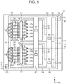
FIG. 1 is a plan view of a semiconductor module. -
FIG. 2 is a sectional view taken along line II-II inFIG. 1 illustrating the semiconductor module. -
FIG. 3 is a sectional view taken along line III-III inFIG. 2 illustrating the semiconductor module. -
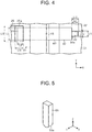
FIG. 4 is an enlarged plan view illustrating a conductive plate. -
FIG. 5 is a perspective view of a lead. -
FIG. 6 is a view illustrating a step of a manufacturing process of the semiconductor module. - An exemplary embodiment of a semiconductor module will be described hereinafter.
- As illustrated in
FIGS. 1 and2 , asemiconductor module 10 includes asubstrate 21 disposed horizontally, two bare chips (semiconductor elements) 31 mounted on thesubstrate 21, and acase 61 fixed to thesubstrate 21. Thesemiconductor module 10 also includes a sealing resin that is not illustrated. InFIGS. 1 to 6 , a horizontal plane is defined by X, Y directions that are orthogonal to each other, and a vertical direction is defined by Z direction. - The
substrate 21 includes aninsulating substrate 22. At two places of theinsulating substrate 22, throughholes 23 extending through theinsulating substrate 22 in a vertical direction (the Z direction) are provided. Oneconductor pattern 24 and fivesignal patterns 25 are provided for each of thebare chips 31 on an upper surface of theinsulating substrate 22. That is, a total of twoconductor patterns 24 and a total of tensignal patterns 25 are provided on theinsulating substrate 22. Each of thesignal patterns 25 extends in the X direction, and the tensignal patterns 25 are disposed parallel to each other in the Y direction. Apad 24a is provided on eachconductor pattern 24. Further, apad 25a and apad 25b are provided at two places, respectively, of each of thesignal patterns 25. - The
bare chip 31 is joined to eachconductor pattern 24. Thebare chip 31 of the present exemplary embodiment is a vertical-type power MOSFET. - As illustrated in
FIG. 3 , each of thebare chips 31 includes asource electrode 33 andsignal electrodes upper surface 32. Thesignal electrodes electrodes signal electrodes bare chips 31. - The
signal electrode 34a is a control signal electrode (a gate electrode). Thesignal electrodes signal electrodes - Areas of the
signal electrodes signal electrode 34a is smaller than an area of thesource electrode 33, which is a separate electrode from thesignal electrode 34a of the plurality ofelectrodes upper surface 32 of thebare chip 31. - As illustrated in
FIG. 2 , each of thebare chips 31 includes adrain electrode 36 as an electrode disposed on alower surface 35 thereof. Thedrain electrode 36 is provided over the entirelower surface 35. Thedrain electrode 36 of eachbare chip 31 is joined to theconductor pattern 24 by a conductive bonding material (not illustrated), such as a solder. - As illustrated in
FIGS. 2 and3 , twoconductive plate assemblies 41, each of which is formed by integrating five conductive plates (bus bars) 42 as conductors with one insulatingmember 48, are provided on an upper surface side of thesubstrate 21. Theconductive plate 42 is disposed on each of the plurality ofsignal electrodes - The
signal electrodes bare chip 31 are connected to thesignal patterns 25 via theconductive plates 42. Among thesignal patterns 25, thesignal pattern 25 that is connected to thesignal electrode 34a via theconductive plate 42 is a control signal pattern. - As illustrated in
FIG. 2 , eachconductive plate 42 is formed by bending a metal plate, and has a rectangular connectingportion 43, afirst extension portion 44, asecond extension portion 45, a first joiningportion 46, and a second joiningportion 47. The connectingportion 43 extends in the X direction. Theextension portions portion 43. The first joiningportion 46 extends in the X direction from a lower end portion of thefirst extension portion 44. The second joiningportion 47 extends in the X direction from a lower end portion of thesecond extension portion 45. The connectingportion 43 is provided between the first joiningportion 46 and the second joiningportion 47. The connectingportion 43 electrically connects the first joiningportion 46 and the second joiningportion 47 via thefirst extension portion 44 and thesecond extension portion 45. A dimension of thefirst extension portion 44 in the vertical direction (the Z direction) is shorter than a dimension of thesecond extension portion 45 in the vertical direction (the Z direction). - Further, as illustrated in
FIG. 4 , an area of the first joiningportion 46 represented by L1 × L2 is smaller than an area of the second joiningportion 47 represented by L3 × L4. Furthermore, the area of each of thesignal electrodes pad 25a represented by L13 × L14. - As illustrated in
FIGS. 2 and3 , the insulatingmember 48 is provided on the connectingportion 43 of theconductive plates 42. One insulatingmember 48 is provided for each set of the fiveconductive plates 42, and the connectingportion 43 of each of theconductive plates 42 extends through the insulatingmember 48. A part of the insulatingmember 48 is located between thefirst extension portion 44 and thesecond extension portion 45. The insulatingmember 48 is formed of a synthetic resin. - The five
conductive plates 42 are fixed to and integrated with the insulating member 48 (integrated into an assembly), with the intervals between theconductive plates 42 in the Y direction maintained. The intervals between the first joiningportions 46 of theconductive plates 42 are the same as the intervals between thesignal electrodes bare chip 31. The intervals between the second joiningportions 47 of theconductive plates 42 are the same as the intervals between thepads 25a of thesignal patterns 25. - The
conductive plates 42 are disposed so that the first joiningportions 46 face thesignal electrodes portions 47 face thepads 25a of thesignal patterns 25. Then, the first joiningportions 46 are joined to thesignal electrodes portions 47 are joined to thepads 25a of thesignal patterns 25 bysolders 52. The solders 51 form fillets between thesignal electrodes portions 46. Further, a surface of the insulatingmember 48 that faces thesubstrate 21 is bonded to the insulatingsubstrate 22 with an adhesive 49. - As illustrated in
FIGS. 1 and2 , thecase 61 is disposed on the upper surface of thesubstrate 21. Thecase 61 includes amain body 62 that has a square frame shape and twoprotrusions 63 that are provided at two corners of themain body 62 so as to extend from an outer surface of themain body 62. Aprojection 64 extends downwardly from each of theprotrusions 63. A spaced distance between the twoprojections 64 is the same as a spaced distance between the throughholes 23 provided in the insulatingsubstrate 22. In addition, each of the twoprojections 64 has such a size as to be insertable into the corresponding throughhole 23. - The
main body 62 includes a pair ofwall portions wall portions support walls first wall portion 65 and thesecond wall portion 66 that are opposite from each other. Two leads 69 are fixed to each of thesupport walls - As illustrated in
FIG. 5 , each lead 69 has a column shape with a roundedlower end 69a. Specifically speaking, part of each lead 69 excluding thelower end 69a is formed in a square column shape, and thelower end 69a is formed in an arc shape. Eachlead 69 extends through thesupport wall case 61. - As illustrated in
FIGS. 2 and3 ,signal terminals 72 are provided in thethird wall portion 70 of themain body 62. Fivesignal terminals 72 are provided for each of thebare chips 31, that is, a total of tensignal terminals 72 is disposed in the Y direction. - Each
signal terminal 72 has a bar shape. A lower end of eachsignal terminal 72 is bent at a right angle to have an L-shape. The lower end of each of thesignal terminals 72 protrudes toward the inside of themain body 62 from thethird wall portion 70. Each of thesignal terminals 72 is integrated with thecase 61. The leads 69 and thesignal terminals 72 are provided so as to extend in the vertical direction (the Z direction) from thesubstrate 21. Therefore, theleads 69 and thesignal terminals 72 do not protrude in the horizontal direction of thesubstrate 21 in a plan view of thesubstrate 21. - The two
projections 64 of thecase 61 are inserted into the two throughholes 23 of the insulatingsubstrate 22. Thewall portions case 61 are bonded to the insulatingsubstrate 22 with an adhesive not illustrated. - Each lead 69 integrated with the
support wall 67 is located above and approximate to thesource electrode 33. Thelower end 69a of each lead 69 is joined to thesource electrode 33 by asolder 53 such that thelower end 69a and thesource electrode 33 do not contact with each other. In this case, the lower ends 69a that are joined to thesource electrodes 33 are joining portions. Eachsolder 53 forms a fillet. - Each lead 69 integrated with the
support wall 68 is located above and approximate to thepad 24a of theconductor pattern 24. Eachlead 69 is joined to thepad 24a by asolder 54 such that thelead 69 and thepad 24a do not contact with each other. Eachsolder 54 forms a fillet. - The lower end of each
signal terminal 72 integrated with thecase 61 is positioned so as to face thepad 25b of thesignal pattern 25. The lower end of eachsignal terminal 72 is joined to thepad 25b of thesignal pattern 25 by asolder 55. - A function of the
semiconductor module 10 of the present exemplary embodiment will be described hereinafter. - When the
semiconductor module 10 is manufactured, the first joiningportions 46 of theconductive plates 42 are joined to thesignal electrodes portions 47 of theconductive plates 42 are joined to thepads 25a of thesignal patterns 25 by soldering. A detailed description will be given hereinafter. - As illustrated in
FIG. 6 , when soldering is performed, solder pastes 51 a and 52a are disposed on thesignal electrodes pads 25a, and the first joiningportions 46 and the second joiningportions 47 of theconductive plates 42 are disposed on the solder pastes 51a and 52a, respectively. In this case, the insulatingmembers 48 are bonded to the insulatingsubstrate 22 with the adhesive 49. - Further, in the present exemplary embodiment, since the
leads 69 and thesignal terminals 72 are also soldered collectively, solder pastes 53a, 54a, and 55a are disposed respectively also on thesource electrodes 33 and thepads case 61 is disposed so that theprojections 64 of thecase 61 are inserted into the throughholes 23 of the insulatingsubstrate 22, so that theleads 69 and thesignal terminals 72 are positioned. The lower ends 69a of theleads 69 and the lower ends of thesignal terminals 72 are brought into contact with the solder pastes 53a, 54a, and 55a, respectively. - The solder pastes 51a, 52a, 53a, 54a, and 55a are melted in a reflow furnace or the like and then hardened, so that the
conductive plates 42, theleads 69, and thesignal terminals 72 are joined by thesolders - The
conductive plates 42 need to stand on their own on the solder pastes 51a and 52a before theconductive plates 42 are joined by thesolders 51 and 52. In the present exemplary embodiment, the weight of the insulatingmembers 48 is applied to theconductive plates 42 by disposing the insulatingmembers 48 on the connectingportions 43. Therefore, the weight applied to thesubstrate 21 from theconductive plates 42 increases, as compared with a case where the insulatingmembers 48 are not provided, so that a center of gravity is stabilized. As a result, theconductive plates 42 are further prevented from falling down. Further, in the present exemplary embodiment, since the insulatingmembers 48 are bonded to the insulatingsubstrate 22, the falling down of theconductive plates 42 is further prevented. - Furthermore, there is a risk that a Manhattan phenomenon may occur due to surface tensions of the melted solder pastes 51a and 52a. However, the occurrence of the Manhattan phenomenon is also prevented by the weight of the insulating
member 48 applied to theconductive plates 42. - In particular, when there is a difference in area between the first joining
portion 46 and the second joiningportion 47 in eachconductive plate 42, the falling down of theconductive plate 42 and the Manhattan phenomenon are more likely to occur due to the area difference. However, according to the present exemplary embodiment, although there is the difference in area between the first joiningportion 46 and the second joiningportion 47 in eachconductive plate 42, the falling down of theconductive plate 42 and the Manhattan phenomenon are prevented by the provision of the insulatingmember 48. - Thus, according to the exemplary embodiment described above, the following effects are obtained.
- (1) The insulating
members 48 are provided on the connectingportions 43 of theconductive plates 42. Therefore, the weight of the insulatingmembers 48 are applied to theconductive plates 42, so that the falling down of theconductive plates 42 before theconductive plates 42 are joined by thesolders 51 and 52 is prevented. - (2) The insulating
members 48 are bonded to the insulatingsubstrate 22 with the adhesive 49. As a result, the falling down of theconductive plates 42 is further prevented. - (3) The plurality of
conductive plates 42 is integrated by the insulatingmembers 48. Therefore, it is not necessary to position theconductive plates 42 individually when joining theconductive plates 42 and therefore the positioning of the plurality ofconductive plates 42 becomes easier. - (4) The lower ends 69a of the
leads 69 are spaced apart from thesource electrodes 33. As a result, thesource electrodes 33 are prevented from being damaged by contacting with theleads 69. - (5) The lower ends 69a of the
leads 69 each have the round shape. Therefore, thesolders 53 that join theleads 69 and thesource electrodes 33 form fillets easily, and thesolders 54 joining theleads 69 and thepads 24a form fillets easily. - (6) Since the
conductive plates 42 are joined to thesignal electrodes pads 25a of thesignal patterns 25 by thesolders 51 and 52, the joining of theconductive plates 42 and joining of theleads 69 are performed collectively. If thesignal electrodes pads 25a of thesignal patterns 25 are connected to each other by bonding wires, joining of the bonding wires and joining of theleads 69 need to be performed separately. In a case where the bonding wires are joined after thecase 61 is attached to thesubstrate 21, acase 61 of an increased size is required for securing the joining region. According to the present exemplary embodiment, the size of thecase 61 does not need to be increased because soldering is performed collectively using theconductive plates 42, so that an increase in the size of thesemiconductor module 10 is prevented. - It is to be noted that the exemplary embodiment may be modified as described below.
- ∘ The insulating
members 48 may not be bonded to the insulatingsubstrate 22. In this case, the insulatingmembers 48 may be or may not be in surface contact with the insulatingsubstrate 22. In either case, the weight of the insulatingmembers 48 is applied to theconductive plates 42, so that the falling down of each of theconductive plates 42 before being joined by thesolders 51 and 52 is prevented. Further, in a case where the insulatingmembers 48 are in surface contact with the insulatingsubstrate 22, a contact area between the insulatingmembers 48 and the insulatingsubstrate 22 is increased, so that theconductive plates 42 hardly fall down. - ∘ Insulating members may be provided individually on the respective
conductive plates 42. That is, the plurality ofconductive plates 42 may not be integrated. - ∘ The number of the
conductive plates 42 may appropriately be changed in accordance with the number of thesignal electrodes - ∘ The adhesive for bonding the insulating
members 48 and the insulatingsubstrate 22 may volatilize in a soldering process or the like. - ∘ The insulating
members 48 may be made of a material other than resin, as long as the insulatingmembers 48 have an insulating property. - ∘ The insulating
members 48 may be bonded to thecase 61. - ∘ The lower ends 69a of the
leads 69 may be in contact with thesource electrodes 33. - ∘ The leads 69 and the
signal terminals 72 may not be integrated with thecase 61. - ∘ The
lower end 69a of each lead 69 may have a flat shape or the like, that is, eachlower end 69a may not have the round shape. - ∘ Each of the
bare chips 31 may be an insulated gate bipolar transistor (IGBT). - ∘ The number of the
bare chips 31, the number of theconductor patterns 24, the number of theleads 69, and the like may be changed appropriately. - ∘ The insulating member may be provided on a body portion of a chip capacitor having a first joining portion, a second joining portion, and the body portion provided between the first joining portion and the second joining portion.
- ∘ The areas of the
signal electrodes - ∘ The intervals between the first joining
portions 46 of theconductive plates 42 may not be the same as the intervals between thesignal electrodes bare chip 31. - ∘ The intervals between the second joining
portions 47 of theconductive plates 42 may not be the same as the intervals between thepads 25a of thesignal patterns 25. - ∘ The area of the first joining
portion 46 may be larger than the area of the second joiningportion 47. -
- 10
- semiconductor module
- 21
- substrate
- 22
- insulating substrate
- 24
- conductor pattern
- 25
- signal pattern
- 31
- bare chip
- 32
- upper surface
- 33
- source electrode
- 34a, 34b, 34c, 34d, 34e
- signal electrode
- 35
- lower surface
- 36
- drain electrode
- 42
- conductive plate
- 43
- connecting portion
- 46
- first joining portion
- 47
- second joining portion
- 48
- insulating member
- 51, 52, 53, 54, 55
- solder
- 69
- lead
- 69a
- lower end
Claims (6)
- A semiconductor module comprising:a substrate;a bare chip including a plurality of electrodes disposed on an upper surface thereof and an electrode disposed on a lower surface thereof, the electrode on the lower surface being mounted on the substrate; anda conductor including a first joining portion that is joined to a control signal electrode of the electrodes disposed on the upper surface of the bare chip, a second joining portion that is joined to a control signal pattern on the substrate, and a connecting portion that electrically connects the first joining portion and the second joining portion, whereinthe connecting portion is provided with an insulating member.
- The semiconductor module according to claim 1, wherein
the semiconductor module comprises a plurality of signal electrodes that includes the control signal electrode and is provided for the one bare chip,
the conductor is a plurality of conductors that are disposed respectively on the plurality of the signal electrodes, and
the connecting portions of the plurality of conductors are fixed by the single insulating member. - The semiconductor module according to claim 1 or 2, wherein the insulating member and the substrate are in surface contact with each other.
- The semiconductor module according to claim 1 or 2, wherein the insulating member and the substrate are bonded to each other.
- The semiconductor module according to any one of claims 1 to 4, wherein
the bare chip is a plurality of the bare chips,
a plurality of leads is formed integrally with a case, the leads being joined to a separate electrode from a signal electrode of a plurality of electrodes disposed on an upper surface of each of the bare chips, and
the leads and the separate electrode are joined to each other without contacting with each other. - The semiconductor module according to claim 5, wherein a joining portion of each of the leads has a round shape.
Applications Claiming Priority (2)
| Application Number | Priority Date | Filing Date | Title |
|---|---|---|---|
| JP2016153084A JP6717103B2 (en) | 2016-08-03 | 2016-08-03 | Semiconductor module |
| PCT/JP2017/018052 WO2018025463A1 (en) | 2016-08-03 | 2017-05-12 | Semiconductor module |
Publications (2)
| Publication Number | Publication Date |
|---|---|
| EP3496141A1 true EP3496141A1 (en) | 2019-06-12 |
| EP3496141A4 EP3496141A4 (en) | 2019-07-17 |
Family
ID=61074071
Family Applications (1)
| Application Number | Title | Priority Date | Filing Date |
|---|---|---|---|
| EP17836570.6A Withdrawn EP3496141A4 (en) | 2016-08-03 | 2017-05-12 | SEMICONDUCTOR MODULE |
Country Status (6)
| Country | Link |
|---|---|
| US (1) | US10770400B2 (en) |
| EP (1) | EP3496141A4 (en) |
| JP (1) | JP6717103B2 (en) |
| KR (1) | KR20190024993A (en) |
| CN (1) | CN109564912A (en) |
| WO (1) | WO2018025463A1 (en) |
Families Citing this family (1)
| Publication number | Priority date | Publication date | Assignee | Title |
|---|---|---|---|---|
| JP7634456B2 (en) * | 2021-09-28 | 2025-02-21 | 三菱電機株式会社 | Semiconductor Device |
Family Cites Families (13)
| Publication number | Priority date | Publication date | Assignee | Title |
|---|---|---|---|---|
| JP3614386B2 (en) | 2001-08-23 | 2005-01-26 | 株式会社ルネサステクノロジ | Power MOSFET |
| JP3904541B2 (en) * | 2003-09-26 | 2007-04-11 | 沖電気工業株式会社 | Manufacturing method of semiconductor device embedded substrate |
| JP2007288044A (en) * | 2006-04-19 | 2007-11-01 | Sumitomo Electric Ind Ltd | Semiconductor device |
| JP5268786B2 (en) * | 2009-06-04 | 2013-08-21 | 三菱電機株式会社 | Semiconductor module |
| JP5659663B2 (en) * | 2010-09-28 | 2015-01-28 | 富士電機株式会社 | Semiconductor device and manufacturing method of semiconductor device |
| JP2012151353A (en) * | 2011-01-20 | 2012-08-09 | Sharp Corp | Semiconductor module |
| CN102148215B (en) * | 2011-01-21 | 2012-06-06 | 哈尔滨理工大学 | Interconnection structure for improving reliability of soldering spot of soft soldering of CCGA (Ceramic Column Grid Array) device and implementation method |
| JP2013004943A (en) | 2011-06-22 | 2013-01-07 | Renesas Electronics Corp | Semiconductor device and manufacturing method thereof |
| JP5708359B2 (en) * | 2011-08-11 | 2015-04-30 | 株式会社デンソー | Semiconductor device and manufacturing method of semiconductor device |
| JP2015080383A (en) | 2013-10-18 | 2015-04-23 | 日本精工株式会社 | Semiconductor module |
| JP6316412B2 (en) * | 2014-05-20 | 2018-04-25 | 三菱電機株式会社 | Power semiconductor device |
| CN105981167B (en) * | 2014-08-12 | 2019-05-28 | 富士电机株式会社 | semiconductor device |
| JP6361448B2 (en) * | 2014-10-15 | 2018-07-25 | 住友電気工業株式会社 | Semiconductor module |
-
2016
- 2016-08-03 JP JP2016153084A patent/JP6717103B2/en not_active Expired - Fee Related
-
2017
- 2017-05-12 CN CN201780047686.1A patent/CN109564912A/en not_active Withdrawn
- 2017-05-12 WO PCT/JP2017/018052 patent/WO2018025463A1/en not_active Ceased
- 2017-05-12 KR KR1020197002978A patent/KR20190024993A/en not_active Abandoned
- 2017-05-12 US US16/322,401 patent/US10770400B2/en not_active Expired - Fee Related
- 2017-05-12 EP EP17836570.6A patent/EP3496141A4/en not_active Withdrawn
Also Published As
| Publication number | Publication date |
|---|---|
| JP6717103B2 (en) | 2020-07-01 |
| EP3496141A4 (en) | 2019-07-17 |
| US20190172788A1 (en) | 2019-06-06 |
| KR20190024993A (en) | 2019-03-08 |
| US10770400B2 (en) | 2020-09-08 |
| JP2018022777A (en) | 2018-02-08 |
| WO2018025463A1 (en) | 2018-02-08 |
| CN109564912A (en) | 2019-04-02 |
Similar Documents
| Publication | Publication Date | Title |
|---|---|---|
| JP5176507B2 (en) | Semiconductor device | |
| CN106171049B (en) | Electronic equipment | |
| EP3226292A1 (en) | Lead frame, semiconductor device, method for manufacturing lead frame, and method for manufacturing semiconductor device | |
| KR102041645B1 (en) | Power semiconductor module | |
| US10229884B2 (en) | Semiconductor device | |
| CN112913009B (en) | Semiconductor device and lead frame material | |
| CN106449531B (en) | Semiconductor device and method of manufacturing the same | |
| US9000571B2 (en) | Surface-mounting light emitting diode device and method for manufacturing the same | |
| CN107211533B (en) | circuit structure | |
| JP4118143B2 (en) | Power circuit equipment | |
| US9974182B2 (en) | Circuit assembly | |
| US10770400B2 (en) | Semiconductor module | |
| JP4651652B2 (en) | Power circuit equipment | |
| JP5533983B2 (en) | Semiconductor device | |
| JP2023011372A (en) | Semiconductor device | |
| US10903147B2 (en) | Semiconductor device | |
| CN113711345B (en) | External terminals for semiconductor modules | |
| JP2006060106A (en) | Lead member and surface mount semiconductor device | |
| JP2576531B2 (en) | Hybrid IC | |
| JPH02201945A (en) | Surface mounting type semiconductor device | |
| JPH0247109B2 (en) | ||
| JP2018018880A (en) | Semiconductor element mounting substrate | |
| JP2023075428A (en) | Semiconductor device | |
| JPH0648875Y2 (en) | Semiconductor device | |
| JP2023043641A (en) | Semiconductor device and manufacturing method thereof |
Legal Events
| Date | Code | Title | Description |
|---|---|---|---|
| PUAI | Public reference made under article 153(3) epc to a published international application that has entered the european phase |
Free format text: ORIGINAL CODE: 0009012 |
|
| 17P | Request for examination filed |
Effective date: 20190116 |
|
| AK | Designated contracting states |
Kind code of ref document: A1 Designated state(s): AL AT BE BG CH CY CZ DE DK EE ES FI FR GB GR HR HU IE IS IT LI LT LU LV MC MK MT NL NO PL PT RO RS SE SI SK SM TR |
|
| AX | Request for extension of the european patent |
Extension state: BA ME |
|
| A4 | Supplementary search report drawn up and despatched |
Effective date: 20190619 |
|
| RIC1 | Information provided on ipc code assigned before grant |
Ipc: H01L 25/07 20060101ALI20190613BHEP Ipc: H01L 21/60 20060101ALI20190613BHEP Ipc: H01L 23/48 20060101AFI20190613BHEP Ipc: H01L 25/18 20060101ALI20190613BHEP |
|
| DAV | Request for validation of the european patent (deleted) | ||
| DAX | Request for extension of the european patent (deleted) | ||
| STAA | Information on the status of an ep patent application or granted ep patent |
Free format text: STATUS: THE APPLICATION HAS BEEN WITHDRAWN |
|
| 18W | Application withdrawn |
Effective date: 20201006 |