EP3492972A1 - Thin-film transistor array substrate and organic light-emitting display device including the same - Google Patents
Thin-film transistor array substrate and organic light-emitting display device including the same Download PDFInfo
- Publication number
- EP3492972A1 EP3492972A1 EP18208168.7A EP18208168A EP3492972A1 EP 3492972 A1 EP3492972 A1 EP 3492972A1 EP 18208168 A EP18208168 A EP 18208168A EP 3492972 A1 EP3492972 A1 EP 3492972A1
- Authority
- EP
- European Patent Office
- Prior art keywords
- insulating film
- active layer
- gate insulating
- transistor
- disposed
- Prior art date
- Legal status (The legal status is an assumption and is not a legal conclusion. Google has not performed a legal analysis and makes no representation as to the accuracy of the status listed.)
- Granted
Links
Images






Classifications
-
- H—ELECTRICITY
- H10—SEMICONDUCTOR DEVICES; ELECTRIC SOLID-STATE DEVICES NOT OTHERWISE PROVIDED FOR
- H10K—ORGANIC ELECTRIC SOLID-STATE DEVICES
- H10K59/00—Integrated devices, or assemblies of multiple devices, comprising at least one organic light-emitting element covered by group H10K50/00
- H10K59/10—OLED displays
- H10K59/12—Active-matrix OLED [AMOLED] displays
- H10K59/121—Active-matrix OLED [AMOLED] displays characterised by the geometry or disposition of pixel elements
- H10K59/1213—Active-matrix OLED [AMOLED] displays characterised by the geometry or disposition of pixel elements the pixel elements being TFTs
-
- G—PHYSICS
- G02—OPTICS
- G02F—OPTICAL DEVICES OR ARRANGEMENTS FOR THE CONTROL OF LIGHT BY MODIFICATION OF THE OPTICAL PROPERTIES OF THE MEDIA OF THE ELEMENTS INVOLVED THEREIN; NON-LINEAR OPTICS; FREQUENCY-CHANGING OF LIGHT; OPTICAL LOGIC ELEMENTS; OPTICAL ANALOGUE/DIGITAL CONVERTERS
- G02F1/00—Devices or arrangements for the control of the intensity, colour, phase, polarisation or direction of light arriving from an independent light source, e.g. switching, gating or modulating; Non-linear optics
- G02F1/01—Devices or arrangements for the control of the intensity, colour, phase, polarisation or direction of light arriving from an independent light source, e.g. switching, gating or modulating; Non-linear optics for the control of the intensity, phase, polarisation or colour
- G02F1/13—Devices or arrangements for the control of the intensity, colour, phase, polarisation or direction of light arriving from an independent light source, e.g. switching, gating or modulating; Non-linear optics for the control of the intensity, phase, polarisation or colour based on liquid crystals, e.g. single liquid crystal display cells
- G02F1/133—Constructional arrangements; Operation of liquid crystal cells; Circuit arrangements
- G02F1/136—Liquid crystal cells structurally associated with a semi-conducting layer or substrate, e.g. cells forming part of an integrated circuit
- G02F1/1362—Active matrix addressed cells
- G02F1/136209—Light shielding layers, e.g. black matrix, incorporated in the active matrix substrate, e.g. structurally associated with the switching element
-
- H—ELECTRICITY
- H10—SEMICONDUCTOR DEVICES; ELECTRIC SOLID-STATE DEVICES NOT OTHERWISE PROVIDED FOR
- H10D—INORGANIC ELECTRIC SEMICONDUCTOR DEVICES
- H10D30/00—Field-effect transistors [FET]
- H10D30/60—Insulated-gate field-effect transistors [IGFET]
- H10D30/67—Thin-film transistors [TFT]
- H10D30/6704—Thin-film transistors [TFT] having supplementary regions or layers in the thin films or in the insulated bulk substrates for controlling properties of the device
- H10D30/6713—Thin-film transistors [TFT] having supplementary regions or layers in the thin films or in the insulated bulk substrates for controlling properties of the device characterised by the properties of the source or drain regions, e.g. compositions or sectional shapes
-
- H—ELECTRICITY
- H10—SEMICONDUCTOR DEVICES; ELECTRIC SOLID-STATE DEVICES NOT OTHERWISE PROVIDED FOR
- H10D—INORGANIC ELECTRIC SEMICONDUCTOR DEVICES
- H10D30/00—Field-effect transistors [FET]
- H10D30/60—Insulated-gate field-effect transistors [IGFET]
- H10D30/67—Thin-film transistors [TFT]
- H10D30/6704—Thin-film transistors [TFT] having supplementary regions or layers in the thin films or in the insulated bulk substrates for controlling properties of the device
- H10D30/6723—Thin-film transistors [TFT] having supplementary regions or layers in the thin films or in the insulated bulk substrates for controlling properties of the device having light shields
-
- H—ELECTRICITY
- H10—SEMICONDUCTOR DEVICES; ELECTRIC SOLID-STATE DEVICES NOT OTHERWISE PROVIDED FOR
- H10D—INORGANIC ELECTRIC SEMICONDUCTOR DEVICES
- H10D30/00—Field-effect transistors [FET]
- H10D30/60—Insulated-gate field-effect transistors [IGFET]
- H10D30/67—Thin-film transistors [TFT]
- H10D30/674—Thin-film transistors [TFT] characterised by the active materials
- H10D30/6755—Oxide semiconductors, e.g. zinc oxide, copper aluminium oxide or cadmium stannate
-
- H—ELECTRICITY
- H10—SEMICONDUCTOR DEVICES; ELECTRIC SOLID-STATE DEVICES NOT OTHERWISE PROVIDED FOR
- H10D—INORGANIC ELECTRIC SEMICONDUCTOR DEVICES
- H10D86/00—Integrated devices formed in or on insulating or conducting substrates, e.g. formed in silicon-on-insulator [SOI] substrates or on stainless steel or glass substrates
- H10D86/01—Manufacture or treatment
- H10D86/021—Manufacture or treatment of multiple TFTs
- H10D86/0221—Manufacture or treatment of multiple TFTs comprising manufacture, treatment or patterning of TFT semiconductor bodies
-
- H—ELECTRICITY
- H10—SEMICONDUCTOR DEVICES; ELECTRIC SOLID-STATE DEVICES NOT OTHERWISE PROVIDED FOR
- H10D—INORGANIC ELECTRIC SEMICONDUCTOR DEVICES
- H10D86/00—Integrated devices formed in or on insulating or conducting substrates, e.g. formed in silicon-on-insulator [SOI] substrates or on stainless steel or glass substrates
- H10D86/40—Integrated devices formed in or on insulating or conducting substrates, e.g. formed in silicon-on-insulator [SOI] substrates or on stainless steel or glass substrates characterised by multiple TFTs
- H10D86/441—Interconnections, e.g. scanning lines
-
- H—ELECTRICITY
- H10—SEMICONDUCTOR DEVICES; ELECTRIC SOLID-STATE DEVICES NOT OTHERWISE PROVIDED FOR
- H10D—INORGANIC ELECTRIC SEMICONDUCTOR DEVICES
- H10D86/00—Integrated devices formed in or on insulating or conducting substrates, e.g. formed in silicon-on-insulator [SOI] substrates or on stainless steel or glass substrates
- H10D86/40—Integrated devices formed in or on insulating or conducting substrates, e.g. formed in silicon-on-insulator [SOI] substrates or on stainless steel or glass substrates characterised by multiple TFTs
- H10D86/481—Integrated devices formed in or on insulating or conducting substrates, e.g. formed in silicon-on-insulator [SOI] substrates or on stainless steel or glass substrates characterised by multiple TFTs integrated with passive devices, e.g. auxiliary capacitors
-
- H—ELECTRICITY
- H10—SEMICONDUCTOR DEVICES; ELECTRIC SOLID-STATE DEVICES NOT OTHERWISE PROVIDED FOR
- H10D—INORGANIC ELECTRIC SEMICONDUCTOR DEVICES
- H10D86/00—Integrated devices formed in or on insulating or conducting substrates, e.g. formed in silicon-on-insulator [SOI] substrates or on stainless steel or glass substrates
- H10D86/40—Integrated devices formed in or on insulating or conducting substrates, e.g. formed in silicon-on-insulator [SOI] substrates or on stainless steel or glass substrates characterised by multiple TFTs
- H10D86/60—Integrated devices formed in or on insulating or conducting substrates, e.g. formed in silicon-on-insulator [SOI] substrates or on stainless steel or glass substrates characterised by multiple TFTs wherein the TFTs are in active matrices
-
- H—ELECTRICITY
- H10—SEMICONDUCTOR DEVICES; ELECTRIC SOLID-STATE DEVICES NOT OTHERWISE PROVIDED FOR
- H10K—ORGANIC ELECTRIC SOLID-STATE DEVICES
- H10K59/00—Integrated devices, or assemblies of multiple devices, comprising at least one organic light-emitting element covered by group H10K50/00
- H10K59/10—OLED displays
- H10K59/12—Active-matrix OLED [AMOLED] displays
- H10K59/121—Active-matrix OLED [AMOLED] displays characterised by the geometry or disposition of pixel elements
- H10K59/1216—Active-matrix OLED [AMOLED] displays characterised by the geometry or disposition of pixel elements the pixel elements being capacitors
-
- H—ELECTRICITY
- H10—SEMICONDUCTOR DEVICES; ELECTRIC SOLID-STATE DEVICES NOT OTHERWISE PROVIDED FOR
- H10K—ORGANIC ELECTRIC SOLID-STATE DEVICES
- H10K59/00—Integrated devices, or assemblies of multiple devices, comprising at least one organic light-emitting element covered by group H10K50/00
- H10K59/10—OLED displays
- H10K59/12—Active-matrix OLED [AMOLED] displays
- H10K59/122—Pixel-defining structures or layers, e.g. banks
-
- H—ELECTRICITY
- H10—SEMICONDUCTOR DEVICES; ELECTRIC SOLID-STATE DEVICES NOT OTHERWISE PROVIDED FOR
- H10K—ORGANIC ELECTRIC SOLID-STATE DEVICES
- H10K59/00—Integrated devices, or assemblies of multiple devices, comprising at least one organic light-emitting element covered by group H10K50/00
- H10K59/10—OLED displays
- H10K59/12—Active-matrix OLED [AMOLED] displays
- H10K59/124—Insulating layers formed between TFT elements and OLED elements
-
- H—ELECTRICITY
- H10—SEMICONDUCTOR DEVICES; ELECTRIC SOLID-STATE DEVICES NOT OTHERWISE PROVIDED FOR
- H10K—ORGANIC ELECTRIC SOLID-STATE DEVICES
- H10K59/00—Integrated devices, or assemblies of multiple devices, comprising at least one organic light-emitting element covered by group H10K50/00
- H10K59/10—OLED displays
- H10K59/12—Active-matrix OLED [AMOLED] displays
- H10K59/126—Shielding, e.g. light-blocking means over the TFTs
-
- H—ELECTRICITY
- H10—SEMICONDUCTOR DEVICES; ELECTRIC SOLID-STATE DEVICES NOT OTHERWISE PROVIDED FOR
- H10K—ORGANIC ELECTRIC SOLID-STATE DEVICES
- H10K59/00—Integrated devices, or assemblies of multiple devices, comprising at least one organic light-emitting element covered by group H10K50/00
- H10K59/10—OLED displays
- H10K59/12—Active-matrix OLED [AMOLED] displays
- H10K59/131—Interconnections, e.g. wiring lines or terminals
Definitions
- the present disclosure relates to a thin-film transistor array substrate including at least one thin-film transistor corresponding to each pixel region, and an organic light-emitting display device including the same.
- a display device is applied to various electronic devices such as TVs, mobile phones, notebooks and tablets. Researches for thinning, weight-saving and low-power consumption for the display device have been continued.
- a typical example of the display device may include a liquid crystal display device (LCD), a plasma display device (PDP), a field emission display device (FED), an electroluminescence display device (ELD), an electro-wetting display device (EWD) and an organic light emitting display device (OLED).
- LCD liquid crystal display device
- PDP plasma display device
- FED field emission display device
- ELD electroluminescence display device
- EWD electro-wetting display device
- OLED organic light emitting display device
- the display panel may include a pair of substrates bonded to each other and a polarizing material or a light emitting material disposed between the pair of substrates.
- one of the pair of substrates may be a thin-film transistor array substrate.
- the thin-film transistor array substrate has a plurality of pixel regions defined within a display region in which an image is displayed and drives each pixel region.
- the thin-film transistor array substrate includes at least one thin-film transistor corresponding to each pixel region.
- the thin-film transistor includes an active layer existing in an island form, a gate electrode overlapping a portion of the active layer, and source and drain electrodes corresponding to both ends of the active layer.
- the gate electrode may be disposed on a gate insulating-film covering at least a portion of the active layer.
- a predetermined amount of charges generated during the process may be charged to the active layer.
- the active layer is vulnerable to an overcharge burst as caused by static electricity.
- the greater a width of the active layer the greater the amount of charges charged in the active layer.
- the overcharge burst may occur more easily, thereby causing defective spots.
- the present disclosure is intended to provide a thin-film transistor array substrate capable of preventing the overcharge burst of the active layer due to the static electricity, and to provide an organic light-emitting display device including the same.
- An embodiment comprises an organic light-emitting diode (OLED) device including a substrate, a conducting layer disposed on the substrate, and a buffer insulating film disposed on the conducting layer.
- An active layer of a transistor is disposed on the buffer insulating film.
- a gate insulating film is disposed on the buffer insulating film over the conducting layer and disposed on the active layer.
- a gate electrode is disposed on the gate insulating film over a channel region of the active layer.
- a first connecting pattern is disposed on the gate insulating film over the conducting line and the active layer. The first connecting pattern is connected to the conducting layer via a first connecting contact hole through the gate insulating film and the buffer insulating film. The first connecting pattern is also connected to the active layer via a second connecting contact hole through the gate insulating film.
- the first connecting pattern has a same material as the gate electrode.
- the transistor comprises a switching transistor of a pixel
- the conducting layer comprises a data line to provide a data voltage to a pixel
- the gate electrode comprises a scan line to drive the switching transistor
- the transistor comprises a driving transistor to drive a light-emitting diode of a pixel
- the gate electrode comprises a driving transistor gate electrode to drive the driving transistor
- the conducting layer comprises a light blocking pattern to block light of the light-emitting diode
- the transistor comprises a sensing transistor to sense a voltage to a light-emitting diode of a pixel, wherein the gate electrode comprises a sensing line to drive the sensing transistor, and wherein the conducting layer comprises a light blocking pattern to block light of the light-emitting diode.
- a light blocking pattern is disposed on the substrate that has a same material as the data line.
- the overlapping regions of the active layer of the switching transistor and the light blocking pattern respectively comprise a first electrode and a second electrode of a storage capacitor of the pixel with the buffer insulating film disposed in between.
- the OLED display device further includes an active layer of a driving transistor disposed on the buffer insulating film.
- An active layer of a sensing transistor is disposed on the buffer insulating film.
- the active layer of the switching transistor has a larger area than the active layer of the driving transistor and the sensing transistor.
- the OLED display device further comprises a reference voltage line disposed on the substrate.
- An active layer of a sensing transistor is disposed on the buffer insulating film.
- the gate insulating film is further disposed on the active layer of the sensing transistor.
- a sense line on the gate insulating film overlaps a channel region of the active layer of the sensing transistor.
- a second connecting pattern is disposed on the gate insulating film. The second connecting pattern is connected to the reference voltage line via a third connecting contact hole through the gate insulating film and the buffer insulating film. The second connecting pattern is connected to a source region of the active layer of the sensing transistor via a fourth connecting contact hole through the gate insulating film.
- the OLED display device further comprises a light blocking pattern disposed on the substrate.
- the buffer insulating film is disposed on the light blocking pattern.
- the gate insulating film is disposed on the buffer insulating film overlapping the light blocking pattern.
- a third connecting pattern is disposed on the gate insulating film. The third connecting pattern is connected to the light blocking pattern via a fifth connecting contact hole through the gate insulating film and the buffer insulating film. The third connecting pattern is connected to a drain region of the active layer of the sensing transistor via a sixth connecting contact hole through the gate insulating film.
- a manufacturing method for manufacturing an organic light emitting diode (OLED) display device.
- a conducting layer is formed on a substrate.
- a buffer insulating film is formed on the conducting layer.
- An active layer of a transistor is formed on the buffer insulating film.
- a gate insulating film is formed on the buffer insulating film over the conducting layer and is formed on the active layer of the transistor.
- a first connecting contact hole is formed through the gate insulating film and the buffer insulating film to expose the conducting layer.
- a second connecting contact hole is formed through the gate insulating film to expose the active layer of the transistor.
- a gate electrode is formed on the gate insulating film over a channel region of the active layer of the transistor. Concurrently with forming the gate electrode, a first connecting pattern is formed on the gate insulating film. The first connecting pattern connects to the conducting layer via the first connecting contact hole. The first connecting pattern also connects to the active layer of the transistor via the second connecting contact hole.
- the transistor comprises a switching transistor of a pixel
- the conducting layer comprises a data line to provide a data voltage to the pixel
- the gate electrode comprises a scan line to drive the switching transistor
- a light blocking pattern is further formed on the substrate concurrently with forming the data line.
- Overlapping regions of the active layer of the switching transistor and the light blocking pattern respectively comprise a first electrode and a second electrode of a storage capacitor of the pixel with the buffer insulating film disposed in between.
- a reference voltage line is formed on the substrate.
- An active layer of a sensing transistor is formed on the buffer insulating film.
- the gate insulating film is further formed on the active layer of the sensing transistor.
- a sense line is formed on the gate insulating film over a channel region of the active layer of the sensing transistor.
- a third connecting contact hole is formed through the gate insulating film and the buffer insulating film to expose the reference voltage line.
- a fourth connecting contact hole is formed through the gate insulating film to expose a source region of the active layer of the sensing transistor.
- a second connecting pattern is formed on the gate insulating film connecting to the reference voltage line via the third connecting contact hole, and connecting to the source region of the active layer of the sensing transistor via the fourth connecting contact hole.
- a light blocking pattern is formed on the substrate.
- the buffer insulating film is further formed on the light blocking pattern.
- the gate insulating film is further formed on the buffer insulating film over the light blocking pattern.
- a fifth connecting contact hole is formed through the gate insulating film and the buffer insulating film to expose the light blocking pattern.
- a sixth connecting contact hole is formed through the gate insulating film to expose a drain region of the active layer of the sensing transistor.
- a third connecting pattern is formed on the gate insulating film connecting to the light blocking pattern via the fifth connecting contact hole and connecting to the drain region of the active layer of the sensing transistor via the sixth connecting contact hole.
- FIGS. 1 to 5 a thin-film transistor array substrate according to one embodiment of the present disclosure and an organic light-emitting display device including the same will be described.
- FIG. 1 shows an organic light-emitting display device according to one embodiment of the present disclosure.
- FIG. 2 shows one example of an equivalent circuit to each pixel region in FIG. 1 .
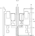
- FIG. 3 shows one example of a plane of a thin-film transistor array substrate corresponding to the equivalent circuit of FIG. 2 .
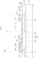
- FIG. 4 shows a cross-section taken in a line A-A' of FIG. 3 .
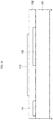
- FIG. 5 shows a cross-section taken in a line B-B'of FIG. 3 .
- the organic light-emitting display device includes a display panel 10 including a plurality of pixel regions PXLs arranged in a matrix within a display region in which images are displayed; a data drive unit 12 for driving data-lines 14 of the display panel 10, a gate drive unit 13 for driving scan-lines 15 of the display panel 10, and a timing controller 11 for controlling a driving timing of each of the data drive unit 12 and the gate drive unit 13.
- the display panel 10 includes scan-lines 15, each corresponding to each horizontal line including pixel regions PXLs arranged in a row in a horizontal direction, and data-lines 14, each corresponding to a vertical line including pixel regions PXLs arranged in a column in a vertical direction.
- the plurality of pixel regions PXLs may be defined by intersecting scan-lines 15 and data-lines 14, and thus may be arranged in a matrix form within the display region AA.
- the display panel 10 includes a first power supply line for supplying a first drive voltage VDD to the plurality of pixel regions PXLs, a second power supply line for supplying a second drive voltage VSS lower than the first drive voltage VDD to the plurality of pixel regions PXLs, and a reference power supply line for supplying a reference voltage VREF to the plurality of pixel regions PXLs.
- the timing controller 11 rearranges digital video data RGB input from the outside according to a resolution of the display panel 10 and supplies the rearranged digital video data RGB' to the data drive unit 12.
- the timing controller 11 generates and supplies a data control signal DDC for controlling an operation timing of the data drive unit 12 and a gate control signal GDC for controlling an operation timing of the gate drive unit 13, based on timing signals such as a vertical synchronization signal Vsync, a horizontal synchronization signal Hsync, a dot clock signal DCLK, and a data enable signal DE.
- the data drive unit 12 converts the rearranged digital video data RGB' into an analog data voltage based on the data control signal DDC. Further, the data drive unit 12 supplies a data signal VDATA to pixel regions corresponding to each horizontal line via the data-line 15 for each horizontal period, based on the rearranged digital video data RGB'.
- the gate drive unit 13 generates and supplies a scan signal SCAN and a sense signal SENSE based on the gate control signal GDC.
- the display panel 10 includes a pair of substrates bonded together facing each other and an organic light-emitting elements array disposed therebetween. Further, one of the pair of substrates may be implemented as a thin-film transistor array substrate.
- the thin-film transistor array substrate has a plurality of pixel regions PXLs defined therein and supplies a driving current to an organic light-emitting element in each pixel region PXL.
- Each of the pixel regions PXLs includes an organic light-emitting element OLED, a storage capacitor Cst, a first thin film transistor T1, a second thin film transistor T2, and a third thin film transistor T3.
- the organic light-emitting element OLED includes an anode and a cathode, and an organic light-emitting layer (not shown) disposed therebetween.
- the organic light-emitting layer includes a hole injection layer, a hole transport layer, a light emitting layer, and an electron transport layer.
- the organic light-emitting layer may further include an electron injection layer.
- the first thin-film transistor T1 is disposed between the first power supply line 16, which supplies the first drive voltage VDD, and the second power supply line, which supplies the second drive voltage VSS below the first drive voltage VDD.
- the first thin-film transistor T1 is connected in series with the organic light-emitting element OLED.
- the second thin-film transistor T2 is disposed between the data-line 14 and the first thin-film transistor T1.
- a data signal VDATA is applied to a first node ND1 between a gate electrode of the first thin-film transistor T1 and the second thin-film transistor T2.
- the storage capacitor Cst is disposed between the first node ND1 and a second node ND2.
- the second node ND2 is a contact point between the first thin-film transistor T1 and the organic light-emitting element OLED.
- the storage capacitor Cst is charged based on the data signal VDATA supplied to the first node ND1 via the second thin-film transistor T2 as is turned on.
- the third thin-film transistor T3 is disposed between the reference power supply line 18 for supplying the reference voltage VREF and the second node ND2.
- the third thin-film transistor T3 is turned on based on the sense signal SENSE from the sense line 17 corresponding to each horizontal line, the second node ND2 is supplied with the reference voltage VREF, or a voltage from the second node ND2 is delivered to the reference power supply line 18.
- the thin-film transistor array substrate 100 of the organic light-emitting display device includes first, second, and third thin-film transistors T1, T2 and T3, and a storage capacitor.
- the thin-film transistor array substrate 100 further includes a scan-line 15 and a sense-line 17, both extending in a first direction (a horizontal direction in FIG. 3 ) and a data-line 14, a first power supply line 16, and a reference power supply line 18, all extending in a second direction (a vertical direction in FIG. 3 ).
- each data-line 14 may correspond to each vertical line, while each of the first power supply line 16 and the reference power supply line 18 may correspond to more than one vertical line.
- the thin-film transistor array substrate 100 includes a first connecting pattern 16b and a second connecting pattern 18b.
- the first connecting pattern 16b is connected to the first power supply line 16 via a first connecting contact-hole 16a and extends in a horizontal direction to a pixel region PXL2 not adjacent to the first power supply line 16.
- the second connecting pattern 18b is connected to the reference power supply line 18 via a second connecting contact-hole 18a and extends in a horizontal direction to a pixel region PXL1 that is not adjacent to the reference power supply line 18.
- the first thin-film transistor T1 includes an active layer 111 and a gate electrode 121 overlapping a portion of the active layer 111.
- the active layer 111 of the first thin-film transistor T1 includes a channel region overlapping the gate electrode 121, and a source region and a drain region respectively disposed at both ends of the channel region.
- One of the source region and the drain region of the active layer 111 of the first thin-film transistor T1 is connected to the first power supply line 16 via the first connecting pattern 16b, while the other thereof is connected to the second node (ND2 in FIG. 2 ) between the organic light-emitting element (OLED in FIG. 2 ) and the third thin-film transistor T3.
- the gate electrode 121 of the first thin-film transistor T1 is connected to the second thin-film transistor T2.
- the second thin-film transistor T2 includes an active layer 112 and a gate electrode defining a portion of the scan-line 15 overlapping the active layer 112.
- the active layer 112 of the second thin-film transistor T2 includes a channel region overlapping a gate electrode defining a portion of the scan-line 15, and source and drain regions respectively disposed at both ends of the channel region.
- one of the source region and the drain region of the active layer 112 of the second thin-film transistor T2 is connected to the data-line 14 via first and second connecting contact-holes 122a and 122b and a connecting pattern 122c, while the other thereof is connected to the gate electrode 121 of the first thin-film transistor T1.
- the third thin-film transistor T3 includes an active layer 113 and a gate electrode defining a portion of the sense-line 17 overlapping the active layer 113.
- the active layer 113 of the third thin-film transistor T3 includes a channel region overlapping a gate electrode defining a portion of the sense-line 17, and a source region and a drain region disposed at both ends of the channel region, respectively.
- one of the source region and the drain region of the active layer 113 of the third thin-film transistor T3 is connected to the reference power supply line 18 via a second connecting pattern 18b, while the other thereof is connected to the second node (ND2 in FIG. 2 ) between the organic light-emitting element (OLED in FIG. 2 ) and the first thin-film transistor T1.
- the first thin-film transistor T1 may be configured to supply the driving current to the organic light-emitting element OLED.
- this may cause a malfunction of the organic light-emitting element OLED, which may lead to poor image quality.
- the thin-film transistor array substrate 100 includes a light-blocking pattern 130 overlapped on the channel region in the active layer 111 of the first thin-film transistor T1 overlapping with the gate electrode 121 of the first thin-film transistor T1 in order to prevent the leakage current from the first thin-film transistor T1 due to light-beams.
- the light-blocking pattern 130 is disposed more adjacent to the substrate (101 in FIG. 4 ) than the active layer 111 of the first thin-film transistor T1.
- the light-blocking pattern is overlapped at least on the channel region in the active layer 111 of the first thin-film transistor T1.
- the light-blocking pattern 130 acts as a first capacitor electrode of the storage capacitor (Cst in FIG. 2 ) connected to the second node ND2 between the first and third thin-film transistors T1 and T3 and the organic light-emitting element OLED .
- one of the source region and the drain region of the active layer 112 of the second thin-film transistor T2 is connected to the first thin-film transistor T1. Said one acts as a second capacitor electrode of the storage capacitor (Cst in FIG. 2 ) connected to the first node ND2 between the first and second thin-film transistors T1 and T2.
- the storage capacitor Cst is positioned in the overlap region between the light-blocking pattern 130 and the active layer 112 of the second thin-film transistor T2. That is, in the overlap region between the light-blocking pattern 130 and the active layer 112 of the second thin-film transistor T2, the storage capacitor Cst is positioned.
- the storage capacitor Cst In order to stably drive each organic light-emitting element OLED during each image frame, the storage capacitor Cst needs to have a capacitance higher than a threshold value.
- the active layer 112 of the second thin-film transistor T2 may have a larger area than that of each of the active layers 111 and 113 of the other thin-film transistors T1 and T3.
- each of the gate electrodes 121, 15 and 17 of the thin-film transistors T1, T2 and T3 may be disposed on each of gate insulating-films covering at least portions of the active layers 111, 112 and 113.
- a patterning process for forming the gate electrode is performed in a state where each of the active layers 111, 112 and 113 has been formed in an island shape. Accordingly, a predetermined amount of charges may be charged to the active layers 111, 112 and 113 as is exposed to the patterning process.
- the active layer 112 of the second thin-film transistor T2 for defining the storage capacitor Cst has the widest width. As a result, a large amount of charges may be charged into the active layer 112 of the second thin-film transistor T2, which, thus, may be vulnerable to an overcharge burst due to static electricity.
- the data-line 14 may be formed prior to formation of the active layer 112 of the second thin-film transistor T2. Further, during the patterning process for forming the gate electrode, a connecting pattern 122c connecting the active layer 112 of the second thin-film transistor T2 and the data-line 14 may be formed.
- the active layer 112 of the thin film transistor T2 is connected to the data line 14 via the connecting pattern 122c. Therefore, during the patterning process for forming the gate electrode, charges charged into the active layer 112 may be discharged via the data line 14, which may suppress an overcharge burst due to static electricity.
- the thin-film transistor array substrate 100 may include the data-line 14 and the light-blocking pattern 130 disposed on the substrate 101; the active layer 112 of the second thin-film transistor T2 disposed on a buffer insulating-film 102 covering the data-line 14 and the light-blocking pattern 130; the gate insulating-film 103 disposed on the buffer insulating-film 102 and covering the data-line 14 and at least a portion of the active layer 112 of the second thin-film transistor T2; the first connecting contact-hole 122a passing through the buffer insulating-film 102 and the gate insulating-film 103 and disposing on a portion of the data-line 14; the second connecting contact-hole 122b passing through the gate insulating-film 103 and disposing on a portion of the active layer 112 of the second thin-film transistor T2; and the connecting pattern 122c disposed on the gate insulating-film 103 and connecting the data-line 14 to
- the thin-film transistor array substrate 100 further includes the scan-line 15 disposed on the gate insulating-film 103.
- a portion of the scan-line 15 overlaps a portion of the active layer 112 of the second thin-film transistor T2, and, thus, act as the gate electrode of the second thin-film transistor T2.
- the active layer 112 of the second thin-film transistor T2 is disposed on the buffer insulating-film 102, and includes a channel region 112a overlapped with the gate electrode defining a portion of the scan-line 15, and a source region 112b and a drain region 112c disposed respectively at both ends of the channel region 112a.
- one (source region 112b in FIG. 4 ) of the source region 112b and the drain region 112c of the active layer 112 of the second thin-film transistor T2 is connected via the first and second connecting contact-holes 122a and 122b and the connecting pattern 122c to the data-line 14 on the substrate 101, while the other (drain region 112c of FIG. 4 ) thereof is connected to the gate electrode 121 of the first thin-film transistor T1 via a gate electrode contact-hole 121a passing through the gate insulating-film 103.
- the active layer 112 of the second thin-film transistor T2 may include an oxide semiconductor material.
- each of the source region 112b and drain region 112c of the active layer 112 of the second thin-film transistor T2 may made of a conducting oxide semiconductor material which may be formed via exposure to an etchant during a patterning process to form the scan-line 15 and the first connecting pattern 16b disposed on the gate insulating-film 103.
- the first connecting pattern 16b which is connected to the first power supply line 16, is disposed on the gate insulating-film 103.
- the first power supply line 16 may be disposed on the substrate 101 together with the data-line 14 and covered with the buffer insulating-film 102.
- the first connecting pattern 16b may be connected to the first power supply line 16 via the first connecting contact-hole 16a passing through the buffer insulating-film 102 and the gate insulating-film 103.
- the first power supply line 16 may be disposed on an interlayer insulating-film (not shown) covering the gate electrode 121, the connecting pattern 122c, the scan-line 15, the sense-line 17, and the first connecting pattern 16b, etc.
- the first connecting contact-hole 16a may pass through the interlayer insulating-film and dispose on a portion of the first connecting pattern 16b.
- the active layer 112 of the second thin-film transistor T2 may be connected to the data-line 14 via the connecting pattern 122c arranged at the same vertical level as the scan-line 15.
- charges that has been charged into the active layer 112 of the second thin-film transistor T2 may be discharged via the data-line 14 while the patterning process to form the scan-line 15 is performed. Therefore, configuring the active layer 112 of the second thin-film transistor T2 having a relatively large area may ensure the capacity of the storage capacitor Cst, while a large amount of charges exceeding the threshold value may be prevented from being charged into the active layer 112 of the second thin-film transistor T2. As a result, the active layer 112 of the second thin-film transistor T2 may be free of the overcharge-burst by static electricity.
- the thin-film transistor array substrate 100 may further include the reference power supply line 18 disposed on the substrate 101 and covered with the buffer insulating-film 102, the active layers 111 and 113 of the first and third thin-film transistors T1 and T3 disposed on the buffer insulating-film 102, and the second connecting pattern 18b, the sense-line 17, first and second connecting patterns 123c and 124c disposed on the gate insulating-film 103.
- the reference power supply line 18 may be disposed on the substrate 101 together with the data-line 14 and may be covered with the buffer insulating-film 102.
- the second connecting pattern 18b disposed on the gate insulating-film 103 may be connected to the reference power supply line 18 via the second connecting contact-hole 18a passing through the buffer insulating-film 102 and the gate insulating-film 103.
- the reference power supply line 18 may be formed on an interlayer insulating-film (not shown) covering the gate electrode 121, the connecting pattern 122c, the scan-line 15, the sense-line 17 and the first connecting pattern 16b, etc.
- the second connecting contact-hole 18a may penetrate the interlayer insulating-film and dispose on the portion of the second connecting pattern 18b.
- the active layer 111 of the first thin-film transistor T1 is disposed on the buffer insulating-film 102.
- the active layer 111 of the first thin-film transistor T1 includes the channel region 111a overlapping the gate electrode 121, and the source region 111b and the drain region 111c respectively disposed on both ends of the channel region 111a.
- the gate electrode 121 of the first thin-film transistor T1 is disposed on the gate insulating-film 103 covering a portion of the active layer 111.
- the gate electrode 121 of the first thin-film transistor T1 is connected to the second thin-film transistor T2 via the gate electrode contact-hole (121a in FIG. 4 ).
- One (source region 111b of FIG. 5 ) of the source region 111b and the drain region 111c of the active layer 111 of the first thin-film transistor T1 is connected to the first power supply line 16 via the first connecting pattern 16a, while the other (drain region 111c of FIG. 5 ) thereof is connected to the light-blocking pattern 130 on the substrate 101 via first and second connecting contact-holes 123a and 123b and the first connecting pattern 123c.
- the active layer 111 of the first thin-film transistor T1 may include an oxide semiconductor material.
- each of the source region 111b and drain region 111c of the active layer 111 of the first thin-film transistor T1 may include a conducting oxide semiconductor material.
- the conducting oxide semiconductor material may be formed via exposure to the etchant during a patterning process to form the scan-line 15 and the first connecting pattern 16b, etc. disposed on the gate insulating-film 103.
- the active layer 113 of the third thin-film transistor T3 is disposed on the buffer insulating-film 102.
- the active layer 113 of the third thin-film transistor T3 includes a channel region 113a overlapping a gate electrode defining a portion of the sense-line 17, and a source region 113b and a drain region 113c respectively disposed on both ends of the channel region 113a.
- one (source region 113b in FIG. 5 ) of the source region 113b and the drain region 113c of the active layer 113 of the third thin-film transistor T3 is connected to the reference power supply line 18 via the second connecting pattern 18a, while the other (drain region 113c of FIG. 5 ) thereof is connected to the light-blocking pattern 130 on the substrate 101 via third and fourth connecting contact-holes 124a and 124b and the second connecting pattern 124c.
- the active layer 113 of the third thin-film transistor T3 may include an oxide semiconductor material.
- each of the source region 113b and drain region 113c of the active layer 113 of the third thin-film transistor T3 may include a conducting oxide semiconductor material.
- the conducting oxide semiconductor material may be formed via exposure to the etchant during a patterning process to form the scan-line 15 and the first connecting pattern 16b, etc. disposed on the gate insulating-film 103.
- the first connecting pattern 16b is connected to the active layer 111 of the first thin-film transistor T1 via a third connecting contact-hole 16c passing through the gate insulating-film 103.
- the first thin-film transistor T1 is connected to the first power supply line 16 via the first connecting pattern 16b.
- the first connecting pattern 123c is connected to the light-blocking pattern 130 via the first connecting contact-hole 123a passing through the buffer insulating-film 102 and the gate insulating-film 103.
- the first connecting pattern 123c is connected to the active layer 111 of the first thin-film transistor T1 via the second connecting contact-hole 123c passing through the gate insulating-film 103.
- the second connecting pattern 124c is connected to the third thin-film transistor T3 via the third connecting contact-hole 124a passing through the gate insulating-film 103.
- the second connecting pattern 124c is connected to the light-blocking pattern 130 via the fourth connecting contact-hole 124b passing through the buffer insulating-film 102 and the gate insulating-film 103.
- the first and third thin-film transistors T1 and T3 are interconnected via the first and second connecting patterns 123c and 124c and the light-blocking pattern 130.
- the second connecting pattern 18b is connected to the active layer 113 of the third thin-film transistor T3 via the fourth connecting contact-hole 18c passing through the gate insulating-film 103.
- the third thin-film transistor T3 is connected to the reference power supply line 18 via the second connecting pattern 18b.
- FIG. 6 shows a method for fabricating a thin-film transistor array substrate according to one embodiment of the present disclosure.
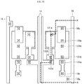
- FIG. 7 to FIG. 14 show structures corresponding to method steps of FIG. 6 , respectively.
- a method for manufacturing a thin-film transistor array substrate includes a step S10 of forming a light-blocking pattern and a data-line on a substrate; a step S20 of forming a buffer insulating-film covering the light-blocking pattern and the data-line; a step S30 of forming an active layer of each thin-film transistor on the buffer insulating-film; a step S40 of forming at least a pre-insulating-film covering the buffer insulating-film and the active layer; a step S50 of forming a plurality of contact-holes passing through at least the pre-insulating-film among the buffer insulating-film and pre-insulating-film; and a step S60 of forming a gate insulating-film and a scan-line by patterning the pre-insulating-film and a conductive film on the pre-insulating-film.
- the light-blocking pattern 130 and the data-line 14 are formed on the substrate 101 (S10).
- the light-blocking pattern 130 corresponds to the portion of each pixel region PXL.
- the light-blocking pattern 130 may be overlapped with the channel region (111a in FIG. 5 ) in the active layer 111 of the first thin-film transistor (T1 in FIG. 3 ), and with the drain region (112C in FIG. 4 ) in the active layer 112 of the second thin-film transistor (T2 in FIG. 3 ).
- the data-line 14 may correspond to each vertical line including pixel regions arranged in a vertical direction among a plurality of pixel regions PXLs, and may extend in a vertical direction.
- two or more vertical lines may correspond to each of the first power supply line 16 and the reference power supply line 18.
- Each of the first power supply line 16 and the reference power supply line 18 may be disposed on the substrate 101, together with the light-blocking pattern 130 and the data-line 14.
- the buffer insulating-film 102 is formed to cover the light-blocking pattern 130, the data-line 14, the first power supply line 16, and the reference power supply line 18 (S20).
- the active layers 111, 112 and 113 of the first, second and third thin-film transistors are formed by patterning an oxide semiconductor material on the buffer insulating-film 102 (S30).
- a pre-insulating-film 103' is formed to cover the buffer insulating-film 102 and the active layers 111, 112 and 113 of the first, second and third thin-film transistors (S40).
- the plurality of contact holes 16a, 16c, 18a, 18c, 121a, 122a, 122b, 123a, 123b, 124a, and 124b is formed by patterning at least the pre-insulating film 103' among the buffer insulating film 102 and the pre-insulating film 103' (S50).
- the first connecting contact-hole 16a passes through the buffer insulating-film 102 and the pre-insulating-film 103' and, thus, disposes on a portion of the first power supply line 16.
- the third connecting contact-hole 16c passes through the pre-insulating-film 103' and disposes on the portion of the active layer 111 of the first thin-film transistor.
- the second connecting contact-hole 18a passes through the buffer insulating-film 102 and the pre-insulating-film 103' and disposes on the portion of the reference power supply line 18.
- the fourth connecting contact-hole 18c passes through the pre-insulating-film 103' and disposes on the portion of the active layer 113 of the third thin-film transistor.
- the gate electrode contact-hole 121a passes through the pre-insulating-film 103' and disposes on a portion of the active layer 112 of the second thin-film transistor.
- the first connecting contact-hole 122a passes through the buffer insulating-film 102 and the pre-insulating-film 103' and disposes on the portion of the data-line 14.
- the second connecting contact-hole 122b passes through the pre-insulating-film 103' and disposes on another portion of the active layer 112 of the second thin-film transistor.
- the first connecting contact-hole 123a passes through the pre-insulating-film 103' and disposes on a portion of the active layer 111 of the first thin-film transistor.
- the second connecting contact-hole 123b passes through the buffer insulating-film 102 and the pre-insulating-film 103' and disposes on a portion of the light-blocking pattern 130.
- the third connecting contact-hole 124a passes through the pre-insulating-film 103' and disposes on a portion of the active layer 113 of the third thin-film transistor.
- the fourth connecting contact-hole 124b passes through the buffer insulating-film 102 and the pre-insulating-film 103' and disposes on another portion of the light-blocking pattern 130.
- the pre-insulating film 103', and a conductive film (not shown) covering the plurality of contact holes 16a, 16c, 18a, 18c, 121a, 122a, 122b, 123a, 123b, 124a, and 124b and the pre-insulating film 103' are simultaneously patterned.
- the scan-line 15, the sense line 17, the first connecting pattern 16b, the second connecting pattern 18b, the gate electrode 121 of the first thin-film transistor, the connecting pattern 122c, the first connecting pattern 123c and the second connecting pattern 124c are formed on the gate insulating-film (S60).
- the gate insulating-film 103 may be formed by patterning the pre-insulating film 103' using, as a mask, the scan-line 15, the sense line 17, the first connecting pattern 16b, the second connecting pattern 18b, the gate electrode 121 of the first thin-film transistor, the connecting pattern 122c, the first connecting pattern 123c and the second connecting pattern 124c.
- each active layer 111, 112 and 113 as covered by the gate insulating-film 103 defines the channel region.
- the source and drain regions which are respectively disposed on both ends of the channel region, are not covered by the gate insulating-film 103 and thus are exposed to the patterning process, and thus are made conductive.
- Each of the scan-line 15 and sense-line 17 corresponds to each horizontal line including pixel regions arranged in a line in a horizontal direction among a plurality of pixel regions PXLs.
- a portion of the scan-line 15 overlaps the channel region (112a in FIG. 4 ) in the active layer 112 of the second thin-film transistor.
- a portion of the sense-line 17 overlaps the channel region (113a in FIG. 5 ) in the active layer 113 of the third thin-film transistor.
- the first connecting pattern 16b is connected to the first power supply line 16 via the first connecting contact-hole 16a.
- the first connecting pattern 16b is connected to the active layer 111 of the first thin-film transistor via the third connecting contact-hole 16c.
- the source region (111b in FIG. 5 ) of the active layer 111 of the first thin-film transistor is connected to the first power supply line 16 via the first connecting pattern 16b.
- the second connecting pattern 18b is connected to the reference power supply line 18 via the second connecting contact-hole 18a.
- the second connecting pattern 18b is connected to the active layer 113 of the third thin-film transistor via the fourth connecting contact-hole 18c.
- the source region 113b of the active layer 113 of the third thin-film transistor is connected to the reference power supply line 18 via the second connecting pattern 18b.
- the gate electrode 121 of the first thin-film transistor is overlapped on the channel region (111a in FIG. 5 ) of the active layer 111 of the first thin-film transistor.
- the gate electrode 121 of the first thin-film transistor is connected to the drain region (112c in FIG. 4 ) of the active layer 112 of the second thin-film transistor via the gate electrode contact-hole 121a.
- the connecting pattern 122c is connected to the data-line 14 via the first connecting contact-hole 122a.
- the connecting pattern 122c is connected to the active layer 112 of the second thin-film transistor via the second connecting contact-hole 122b.
- the source region (112b in FIG. 4 ) of the active layer 112 of the second thin-film transistor is connected to the data-line 14 via the connecting pattern 122c.
- the first connecting pattern 123c is connected to the active layer 111 of the first thin-film transistor via the first connecting contact-hole 123a.
- the first connecting pattern 123c is connected to the light-blocking pattern 130 via the second connecting contact-hole 123b.
- the second connecting pattern 124c is connected to the active layer 113 of the third thin-film transistor via the third connecting contact-hole 124a.
- the second connecting pattern 124c is connected to the light-blocking pattern 130 via the fourth connecting contact-hole 124b.
- the drain region (111c in FIG. 5 ) of the active layer 111 of the first thin-film transistor and the drain region (113c in FIG. 5 ) of the active layer 113 of the third thin-film transistor are connected to each other via the first and second connecting patterns 123c and 124c and the light-blocking pattern 130.
- the step S10 of forming the data-line 14 together with the light-blocking pattern 130 is performed before the step S30 of forming the active layers 111, 112 and 113.
- the step S50 of forming the contact-holes is performed prior to the step S60 of forming the scan-line 15.
- the active layers 111, 112 and 113 as exposed to the patterning process are connected to other lines or patterns via the contact-holes.
- charges may be discharged from the active layers 111, 112 and 113. Therefore, the overcharge burst in the active layers 111, 112 and 113 due to static electricity may be prevented.
Landscapes
- Physics & Mathematics (AREA)
- Engineering & Computer Science (AREA)
- Microelectronics & Electronic Packaging (AREA)
- Nonlinear Science (AREA)
- General Physics & Mathematics (AREA)
- Mathematical Physics (AREA)
- Crystallography & Structural Chemistry (AREA)
- Chemical & Material Sciences (AREA)
- Optics & Photonics (AREA)
- Geometry (AREA)
- Electroluminescent Light Sources (AREA)
- Devices For Indicating Variable Information By Combining Individual Elements (AREA)
- Thin Film Transistor (AREA)
- Computer Hardware Design (AREA)
- Theoretical Computer Science (AREA)
Abstract
Description
- The present disclosure relates to a thin-film transistor array substrate including at least one thin-film transistor corresponding to each pixel region, and an organic light-emitting display device including the same.
- A display device is applied to various electronic devices such as TVs, mobile phones, notebooks and tablets. Researches for thinning, weight-saving and low-power consumption for the display device have been continued.
- A typical example of the display device may include a liquid crystal display device (LCD), a plasma display device (PDP), a field emission display device (FED), an electroluminescence display device (ELD), an electro-wetting display device (EWD) and an organic light emitting display device (OLED).
- The display panel may include a pair of substrates bonded to each other and a polarizing material or a light emitting material disposed between the pair of substrates.
- In this connection, one of the pair of substrates may be a thin-film transistor array substrate. The thin-film transistor array substrate has a plurality of pixel regions defined within a display region in which an image is displayed and drives each pixel region. The thin-film transistor array substrate includes at least one thin-film transistor corresponding to each pixel region.
- In a conventional thin-film transistor array substrate, the thin-film transistor includes an active layer existing in an island form, a gate electrode overlapping a portion of the active layer, and source and drain electrodes corresponding to both ends of the active layer.
- Further, in order to reduce a leakage current from a channel corresponding to an overlapping region between the active layer and the gate electrode, the gate electrode may be disposed on a gate insulating-film covering at least a portion of the active layer.
- In this case, during a patterning process to form the gate electrode, a remaining portion of the active layer that does not overlap the gate electrode is exposed to the patterning process. Thus, a predetermined amount of charges generated during the process may be charged to the active layer. In the state where the predetermined amount of charges have been charged, the active layer is vulnerable to an overcharge burst as caused by static electricity.
- In particular, the greater a width of the active layer, the greater the amount of charges charged in the active layer. As a result, the overcharge burst may occur more easily, thereby causing defective spots.
- An invention is defined in the claims. The present disclosure is intended to provide a thin-film transistor array substrate capable of preventing the overcharge burst of the active layer due to the static electricity, and to provide an organic light-emitting display device including the same.
- The purposes of the present disclosure are not limited to the above-mentioned purposes. Other purposes and advantages of the present disclosure, as not mentioned above, may be understood from the following descriptions and more clearly understood from the embodiments of the present disclosure. Further, it will be readily appreciated that the objects and advantages of the present disclosure may be realized by features and combinations thereof as disclosed in the claims.
- An embodiment comprises an organic light-emitting diode (OLED) device including a substrate, a conducting layer disposed on the substrate, and a buffer insulating film disposed on the conducting layer. An active layer of a transistor is disposed on the buffer insulating film. A gate insulating film is disposed on the buffer insulating film over the conducting layer and disposed on the active layer. A gate electrode is disposed on the gate insulating film over a channel region of the active layer. A first connecting pattern is disposed on the gate insulating film over the conducting line and the active layer. The first connecting pattern is connected to the conducting layer via a first connecting contact hole through the gate insulating film and the buffer insulating film. The first connecting pattern is also connected to the active layer via a second connecting contact hole through the gate insulating film. The first connecting pattern has a same material as the gate electrode.
- In an embodiment, the transistor comprises a switching transistor of a pixel, the conducting layer comprises a data line to provide a data voltage to a pixel, and the gate electrode comprises a scan line to drive the switching transistor.
- In another embodiment, the transistor comprises a driving transistor to drive a light-emitting diode of a pixel, wherein the gate electrode comprises a driving transistor gate electrode to drive the driving transistor, and wherein the conducting layer comprises a light blocking pattern to block light of the light-emitting diode.
- In another embodiment, the transistor comprises a sensing transistor to sense a voltage to a light-emitting diode of a pixel, wherein the gate electrode comprises a sensing line to drive the sensing transistor, and wherein the conducting layer comprises a light blocking pattern to block light of the light-emitting diode.
- In an embodiment, a light blocking pattern is disposed on the substrate that has a same material as the data line. The overlapping regions of the active layer of the switching transistor and the light blocking pattern respectively comprise a first electrode and a second electrode of a storage capacitor of the pixel with the buffer insulating film disposed in between.
- In an embodiment, the OLED display device further includes an active layer of a driving transistor disposed on the buffer insulating film. An active layer of a sensing transistor is disposed on the buffer insulating film. The active layer of the switching transistor has a larger area than the active layer of the driving transistor and the sensing transistor.
- In an embodiment, the OLED display device further comprises a reference voltage line disposed on the substrate. An active layer of a sensing transistor is disposed on the buffer insulating film. The gate insulating film is further disposed on the active layer of the sensing transistor. A sense line on the gate insulating film overlaps a channel region of the active layer of the sensing transistor. A second connecting pattern is disposed on the gate insulating film. The second connecting pattern is connected to the reference voltage line via a third connecting contact hole through the gate insulating film and the buffer insulating film. The second connecting pattern is connected to a source region of the active layer of the sensing transistor via a fourth connecting contact hole through the gate insulating film.
- In an embodiment, the OLED display device further comprises a light blocking pattern disposed on the substrate. The buffer insulating film is disposed on the light blocking pattern. The gate insulating film is disposed on the buffer insulating film overlapping the light blocking pattern. A third connecting pattern is disposed on the gate insulating film. The third connecting pattern is connected to the light blocking pattern via a fifth connecting contact hole through the gate insulating film and the buffer insulating film. The third connecting pattern is connected to a drain region of the active layer of the sensing transistor via a sixth connecting contact hole through the gate insulating film.
- In another aspect, a manufacturing method is provided for manufacturing an organic light emitting diode (OLED) display device. A conducting layer is formed on a substrate. A buffer insulating film is formed on the conducting layer. An active layer of a transistor is formed on the buffer insulating film. A gate insulating film is formed on the buffer insulating film over the conducting layer and is formed on the active layer of the transistor. A first connecting contact hole is formed through the gate insulating film and the buffer insulating film to expose the conducting layer. A second connecting contact hole is formed through the gate insulating film to expose the active layer of the transistor. A gate electrode is formed on the gate insulating film over a channel region of the active layer of the transistor. Concurrently with forming the gate electrode, a first connecting pattern is formed on the gate insulating film. The first connecting pattern connects to the conducting layer via the first connecting contact hole. The first connecting pattern also connects to the active layer of the transistor via the second connecting contact hole.
- In an embodiment, the transistor comprises a switching transistor of a pixel, the conducting layer comprises a data line to provide a data voltage to the pixel, and the gate electrode comprises a scan line to drive the switching transistor.
- In an embodiment, a light blocking pattern is further formed on the substrate concurrently with forming the data line. Overlapping regions of the active layer of the switching transistor and the light blocking pattern respectively comprise a first electrode and a second electrode of a storage capacitor of the pixel with the buffer insulating film disposed in between.
- In an embodiment, a reference voltage line is formed on the substrate. An active layer of a sensing transistor is formed on the buffer insulating film. The gate insulating film is further formed on the active layer of the sensing transistor. A sense line is formed on the gate insulating film over a channel region of the active layer of the sensing transistor. A third connecting contact hole is formed through the gate insulating film and the buffer insulating film to expose the reference voltage line. A fourth connecting contact hole is formed through the gate insulating film to expose a source region of the active layer of the sensing transistor. A second connecting pattern is formed on the gate insulating film connecting to the reference voltage line via the third connecting contact hole, and connecting to the source region of the active layer of the sensing transistor via the fourth connecting contact hole.
- In an embodiment, a light blocking pattern is formed on the substrate. The buffer insulating film is further formed on the light blocking pattern. The gate insulating film is further formed on the buffer insulating film over the light blocking pattern. A fifth connecting contact hole is formed through the gate insulating film and the buffer insulating film to expose the light blocking pattern. A sixth connecting contact hole is formed through the gate insulating film to expose a drain region of the active layer of the sensing transistor. A third connecting pattern is formed on the gate insulating film connecting to the light blocking pattern via the fifth connecting contact hole and connecting to the drain region of the active layer of the sensing transistor via the sixth connecting contact hole.
-
-
FIG. 1 shows an organic light-emitting display device according to one embodiment of the present disclosure. -
FIG. 2 shows one example of an equivalent circuit to each pixel region inFIG. 1 . -
FIG. 3 shows one example of a plane of a thin-film transistor array substrate corresponding to the equivalent circuit ofFIG. 2 . -
FIG. 4 shows a cross-section taken in a line A-A' ofFIG. 3 . -
FIG. 5 shows a cross-section taken in a line B-B' ofFIG. 3 . -
FIG. 6 shows a method for fabricating a thin-film transistor array substrate according to one embodiment of the present disclosure. -
FIGS 7 to 14 show structures corresponding to method steps ofFIG. 6 . - Examples of various embodiments are illustrated and described further below. It will be understood that the description herein is not intended to limit the claims to the specific embodiments described. On the contrary, it is intended to cover alternatives, modifications, and equivalents as may be included within the spirit and scope of the present disclosure as defined by the appended claims.
- The same reference numbers in different figures denote the same or similar elements, and as such perform similar functionality. Further, descriptions and details of well-known steps and elements are omitted for simplicity of the description. Furthermore, in the following detailed description of the present disclosure, numerous specific details are set forth in order to provide a thorough understanding of the present disclosure. However, it will be understood that the present disclosure may be practiced without these specific details. In other instances, well-known methods, procedures, components, and circuits have not been described in detail so as not to unnecessarily obscure aspects of the present disclosure.
- It will be understood that, although the terms "first", "second", "third", and so on may be used herein to describe various elements, components, regions, layers and/or sections, these elements, components, regions, layers and/or sections should not be limited by these terms. These terms are used to distinguish one element, component, region, layer or section from another element, component, region, layer or section. Thus, a first element, component, region, layer or section described below could be termed a second element, component, region, layer or section, without departing from the spirit and scope of the present disclosure.
- It will be understood that when an element or layer is referred to as being "connected to", or "coupled to" another element or layer, it can be directly on, connected to, or coupled to the other element or layer, or one or more intervening elements or layers may be present. In addition, it will also be understood that when an element or layer is referred to as being "between" two elements or layers, it can be the only element or layer between the two elements or layers, or one or more intervening elements or layers may also be present.
- The terminology used herein is for describing particular embodiments only and is not intended to be limiting of the present disclosure. As used herein, the singular forms "a" and "an" are intended to include the plural forms as well, unless the context clearly indicates otherwise. It will be further understood that the terms "comprise", "comprising", "include", and "including" when used in this specification, specify the presence of the stated features, integers, operations, elements, and/or components, but do not preclude the presence or addition of one or more other features, integers, operations, elements, components, and/or portions thereof. As used herein, the term "and/or" includes any and all combinations of one or more of the associated listed items. Expression such as "at least one of' when preceding a list of elements may modify the entire list of elements and may not modify the individual elements of the list.
- Unless otherwise defined, all terms including technical and scientific terms used herein have the same meaning as commonly understood by one of ordinary skill in the art to which this inventive concept belongs. It will be further understood that terms, such as those defined in commonly used dictionaries, should be interpreted as having a meaning that is consistent with their meaning in the context of the relevant art and will not be interpreted in an idealized or overly formal sense unless expressly so defined herein.
- Hereinafter, a thin-film transistor array substrate according to various embodiments of the present disclosure and an organic light-emitting display device including the same will be described in detail with reference to the accompanying drawings.
- First, referring to
FIGS. 1 to 5 , a thin-film transistor array substrate according to one embodiment of the present disclosure and an organic light-emitting display device including the same will be described. -
FIG. 1 shows an organic light-emitting display device according to one embodiment of the present disclosure.FIG. 2 shows one example of an equivalent circuit to each pixel region inFIG. 1 .FIG. 3 shows one example of a plane of a thin-film transistor array substrate corresponding to the equivalent circuit ofFIG. 2 .FIG. 4 shows a cross-section taken in a line A-A' ofFIG. 3 .FIG. 5 shows a cross-section taken in a line B-B'ofFIG. 3 . - As shown in
FIG. 1 , the organic light-emitting display device according to one embodiment of the present disclosure includes adisplay panel 10 including a plurality of pixel regions PXLs arranged in a matrix within a display region in which images are displayed; adata drive unit 12 for driving data-lines 14 of thedisplay panel 10, agate drive unit 13 for driving scan-lines 15 of thedisplay panel 10, and atiming controller 11 for controlling a driving timing of each of the data driveunit 12 and thegate drive unit 13. - Further, the
display panel 10 includes scan-lines 15, each corresponding to each horizontal line including pixel regions PXLs arranged in a row in a horizontal direction, and data-lines 14, each corresponding to a vertical line including pixel regions PXLs arranged in a column in a vertical direction. The plurality of pixel regions PXLs may be defined by intersecting scan-lines 15 and data-lines 14, and thus may be arranged in a matrix form within the display region AA. - Further, the
display panel 10 includes a first power supply line for supplying a first drive voltage VDD to the plurality of pixel regions PXLs, a second power supply line for supplying a second drive voltage VSS lower than the first drive voltage VDD to the plurality of pixel regions PXLs, and a reference power supply line for supplying a reference voltage VREF to the plurality of pixel regions PXLs. - The
timing controller 11 rearranges digital video data RGB input from the outside according to a resolution of thedisplay panel 10 and supplies the rearranged digital video data RGB' to the data driveunit 12. - Further, the
timing controller 11 generates and supplies a data control signal DDC for controlling an operation timing of the data driveunit 12 and a gate control signal GDC for controlling an operation timing of thegate drive unit 13, based on timing signals such as a vertical synchronization signal Vsync, a horizontal synchronization signal Hsync, a dot clock signal DCLK, and a data enable signal DE. - The data drive
unit 12 converts the rearranged digital video data RGB' into an analog data voltage based on the data control signal DDC. Further, the data driveunit 12 supplies a data signal VDATA to pixel regions corresponding to each horizontal line via the data-line 15 for each horizontal period, based on the rearranged digital video data RGB'. - The
gate drive unit 13 generates and supplies a scan signal SCAN and a sense signal SENSE based on the gate control signal GDC. - Although not separately shown, the
display panel 10 includes a pair of substrates bonded together facing each other and an organic light-emitting elements array disposed therebetween. Further, one of the pair of substrates may be implemented as a thin-film transistor array substrate. The thin-film transistor array substrate has a plurality of pixel regions PXLs defined therein and supplies a driving current to an organic light-emitting element in each pixel region PXL. - Each of the pixel regions PXLs includes an organic light-emitting element OLED, a storage capacitor Cst, a first thin film transistor T1, a second thin film transistor T2, and a third thin film transistor T3.
- The organic light-emitting element OLED includes an anode and a cathode, and an organic light-emitting layer (not shown) disposed therebetween. In one example, the organic light-emitting layer includes a hole injection layer, a hole transport layer, a light emitting layer, and an electron transport layer. Alternatively, the organic light-emitting layer may further include an electron injection layer.
- The first thin-film transistor T1 is disposed between the first
power supply line 16, which supplies the first drive voltage VDD, and the second power supply line, which supplies the second drive voltage VSS below the first drive voltage VDD. The first thin-film transistor T1 is connected in series with the organic light-emitting element OLED. - The second thin-film transistor T2 is disposed between the data-
line 14 and the first thin-film transistor T1. When the second thin-film transistor T2 is turned on based on the scan signal SCAN from the scan-line 15, a data signal VDATA is applied to a first node ND1 between a gate electrode of the first thin-film transistor T1 and the second thin-film transistor T2. - The storage capacitor Cst is disposed between the first node ND1 and a second node ND2. The second node ND2 is a contact point between the first thin-film transistor T1 and the organic light-emitting element OLED.
- The storage capacitor Cst is charged based on the data signal VDATA supplied to the first node ND1 via the second thin-film transistor T2 as is turned on.
- The third thin-film transistor T3 is disposed between the reference
power supply line 18 for supplying the reference voltage VREF and the second node ND2. When the third thin-film transistor T3 is turned on based on the sense signal SENSE from thesense line 17 corresponding to each horizontal line, the second node ND2 is supplied with the reference voltage VREF, or a voltage from the second node ND2 is delivered to the referencepower supply line 18. - As shown in
FIG. 3 , the thin-filmtransistor array substrate 100 of the organic light-emitting display device according to one embodiment of the present disclosure includes first, second, and third thin-film transistors T1, T2 and T3, and a storage capacitor. - Further, the thin-film
transistor array substrate 100 further includes a scan-line 15 and a sense-line 17, both extending in a first direction (a horizontal direction inFIG. 3 ) and a data-line 14, a firstpower supply line 16, and a referencepower supply line 18, all extending in a second direction (a vertical direction inFIG. 3 ). - In this connection, each data-
line 14 may correspond to each vertical line, while each of the firstpower supply line 16 and the referencepower supply line 18 may correspond to more than one vertical line. - The thin-film
transistor array substrate 100 includes a first connectingpattern 16b and a second connectingpattern 18b. The first connectingpattern 16b is connected to the firstpower supply line 16 via a first connecting contact-hole 16a and extends in a horizontal direction to a pixel region PXL2 not adjacent to the firstpower supply line 16. The second connectingpattern 18b is connected to the referencepower supply line 18 via a second connecting contact-hole 18a and extends in a horizontal direction to a pixel region PXL1 that is not adjacent to the referencepower supply line 18. - The first thin-film transistor T1 includes an
active layer 111 and agate electrode 121 overlapping a portion of theactive layer 111. - The
active layer 111 of the first thin-film transistor T1 includes a channel region overlapping thegate electrode 121, and a source region and a drain region respectively disposed at both ends of the channel region. - One of the source region and the drain region of the
active layer 111 of the first thin-film transistor T1 is connected to the firstpower supply line 16 via the first connectingpattern 16b, while the other thereof is connected to the second node (ND2 inFIG. 2 ) between the organic light-emitting element (OLED inFIG. 2 ) and the third thin-film transistor T3. - Further, the
gate electrode 121 of the first thin-film transistor T1 is connected to the second thin-film transistor T2. - The second thin-film transistor T2 includes an
active layer 112 and a gate electrode defining a portion of the scan-line 15 overlapping theactive layer 112. - The
active layer 112 of the second thin-film transistor T2 includes a channel region overlapping a gate electrode defining a portion of the scan-line 15, and source and drain regions respectively disposed at both ends of the channel region. In this connection, one of the source region and the drain region of theactive layer 112 of the second thin-film transistor T2 is connected to the data-line 14 via first and second connecting contact-holes pattern 122c, while the other thereof is connected to thegate electrode 121 of the first thin-film transistor T1. - The third thin-film transistor T3 includes an
active layer 113 and a gate electrode defining a portion of the sense-line 17 overlapping theactive layer 113. - The
active layer 113 of the third thin-film transistor T3 includes a channel region overlapping a gate electrode defining a portion of the sense-line 17, and a source region and a drain region disposed at both ends of the channel region, respectively. In this connection, one of the source region and the drain region of theactive layer 113 of the third thin-film transistor T3 is connected to the referencepower supply line 18 via a second connectingpattern 18b, while the other thereof is connected to the second node (ND2 inFIG. 2 ) between the organic light-emitting element (OLED inFIG. 2 ) and the first thin-film transistor T1. - The first thin-film transistor T1 may be configured to supply the driving current to the organic light-emitting element OLED. In this regard, when a leakage current occurs from the first thin-film transistor T1, this may cause a malfunction of the organic light-emitting element OLED, which may lead to poor image quality.
- Therefore, the thin-film
transistor array substrate 100 includes a light-blockingpattern 130 overlapped on the channel region in theactive layer 111 of the first thin-film transistor T1 overlapping with thegate electrode 121 of the first thin-film transistor T1 in order to prevent the leakage current from the first thin-film transistor T1 due to light-beams. - The light-blocking
pattern 130 is disposed more adjacent to the substrate (101 inFIG. 4 ) than theactive layer 111 of the first thin-film transistor T1. The light-blocking pattern is overlapped at least on the channel region in theactive layer 111 of the first thin-film transistor T1. - Further, the light-blocking
pattern 130 acts as a first capacitor electrode of the storage capacitor (Cst inFIG. 2 ) connected to the second node ND2 between the first and third thin-film transistors T1 and T3 and the organic light-emitting element OLED . - Further, one of the source region and the drain region of the
active layer 112 of the second thin-film transistor T2 is connected to the first thin-film transistor T1. Said one acts as a second capacitor electrode of the storage capacitor (Cst inFIG. 2 ) connected to the first node ND2 between the first and second thin-film transistors T1 and T2. - That is, in the overlap region between the light-blocking
pattern 130 and theactive layer 112 of the second thin-film transistor T2, the storage capacitor Cst is positioned. - In order to stably drive each organic light-emitting element OLED during each image frame, the storage capacitor Cst needs to have a capacitance higher than a threshold value.
- In order to secure the capacity of the storage capacitor Cst, it is necessary to increase the overlap region between the
active layer 112 of the second thin-film transistor T2 and the light-blockingpattern 130. Thus, theactive layer 112 of the second thin-film transistor T2 may have a larger area than that of each of theactive layers - Further, in order to reduce the leakage current from each of the
active layers gate electrodes active layers - That is, a patterning process for forming the gate electrode is performed in a state where each of the
active layers active layers - Particularly, among the
active layers active layer 112 of the second thin-film transistor T2 for defining the storage capacitor Cst has the widest width. As a result, a large amount of charges may be charged into theactive layer 112 of the second thin-film transistor T2, which, thus, may be vulnerable to an overcharge burst due to static electricity. - To solve this problem, in the thin-film
transistor array substrate 100 in accordance with one embodiment of the present disclosure, the data-line 14 may be formed prior to formation of theactive layer 112 of the second thin-film transistor T2. Further, during the patterning process for forming the gate electrode, a connectingpattern 122c connecting theactive layer 112 of the second thin-film transistor T2 and the data-line 14 may be formed. - That is, in the patterning process for forming the gate electrode, the
active layer 112 of the thin film transistor T2 is connected to thedata line 14 via the connectingpattern 122c. Therefore, during the patterning process for forming the gate electrode, charges charged into theactive layer 112 may be discharged via thedata line 14, which may suppress an overcharge burst due to static electricity. - Specifically, as shown in
FIG. 4 , the thin-filmtransistor array substrate 100 according to one embodiment of the present disclosure may include the data-line 14 and the light-blockingpattern 130 disposed on thesubstrate 101; theactive layer 112 of the second thin-film transistor T2 disposed on a buffer insulating-film 102 covering the data-line 14 and the light-blockingpattern 130; the gate insulating-film 103 disposed on the buffer insulating-film 102 and covering the data-line 14 and at least a portion of theactive layer 112 of the second thin-film transistor T2; the first connecting contact-hole 122a passing through the buffer insulating-film 102 and the gate insulating-film 103 and disposing on a portion of the data-line 14; the second connecting contact-hole 122b passing through the gate insulating-film 103 and disposing on a portion of theactive layer 112 of the second thin-film transistor T2; and the connectingpattern 122c disposed on the gate insulating-film 103 and connecting the data-line 14 to theactive layer 112 of the second thin-film transistor T2 via the first and second connecting contact-holes - Further, the thin-film
transistor array substrate 100 further includes the scan-line 15 disposed on the gate insulating-film 103. In this connection, a portion of the scan-line 15 overlaps a portion of theactive layer 112 of the second thin-film transistor T2, and, thus, act as the gate electrode of the second thin-film transistor T2. - The
active layer 112 of the second thin-film transistor T2 is disposed on the buffer insulating-film 102, and includes achannel region 112a overlapped with the gate electrode defining a portion of the scan-line 15, and asource region 112b and adrain region 112c disposed respectively at both ends of thechannel region 112a. - In this connection, one (
source region 112b inFIG. 4 ) of thesource region 112b and thedrain region 112c of theactive layer 112 of the second thin-film transistor T2 is connected via the first and second connecting contact-holes pattern 122c to the data-line 14 on thesubstrate 101, while the other (drainregion 112c ofFIG. 4 ) thereof is connected to thegate electrode 121 of the first thin-film transistor T1 via a gate electrode contact-hole 121a passing through the gate insulating-film 103. - Further, the
active layer 112 of the second thin-film transistor T2 may include an oxide semiconductor material. In this case, each of thesource region 112b and drainregion 112c of theactive layer 112 of the second thin-film transistor T2 may made of a conducting oxide semiconductor material which may be formed via exposure to an etchant during a patterning process to form the scan-line 15 and the first connectingpattern 16b disposed on the gate insulating-film 103. - The first connecting
pattern 16b, which is connected to the firstpower supply line 16, is disposed on the gate insulating-film 103. - Although not separately shown, the first
power supply line 16 may be disposed on thesubstrate 101 together with the data-line 14 and covered with the buffer insulating-film 102. In this case, the first connectingpattern 16b may be connected to the firstpower supply line 16 via the first connecting contact-hole 16a passing through the buffer insulating-film 102 and the gate insulating-film 103. - Unlike the data-
line 14, the firstpower supply line 16 may be disposed on an interlayer insulating-film (not shown) covering thegate electrode 121, the connectingpattern 122c, the scan-line 15, the sense-line 17, and the first connectingpattern 16b, etc. In this case, the first connecting contact-hole 16a may pass through the interlayer insulating-film and dispose on a portion of the first connectingpattern 16b. - In this manner, according to one embodiment of the present disclosure, the
active layer 112 of the second thin-film transistor T2 may be connected to the data-line 14 via the connectingpattern 122c arranged at the same vertical level as the scan-line 15. Thus, charges that has been charged into theactive layer 112 of the second thin-film transistor T2 may be discharged via the data-line 14 while the patterning process to form the scan-line 15 is performed. Therefore, configuring theactive layer 112 of the second thin-film transistor T2 having a relatively large area may ensure the capacity of the storage capacitor Cst, while a large amount of charges exceeding the threshold value may be prevented from being charged into theactive layer 112 of the second thin-film transistor T2. As a result, theactive layer 112 of the second thin-film transistor T2 may be free of the overcharge-burst by static electricity. - In addition, as shown in
FIG. 5 , the thin-filmtransistor array substrate 100 according to one embodiment of the present disclosure may further include the referencepower supply line 18 disposed on thesubstrate 101 and covered with the buffer insulating-film 102, theactive layers film 102, and the second connectingpattern 18b, the sense-line 17, first and second connectingpatterns film 103. - The reference
power supply line 18 may be disposed on thesubstrate 101 together with the data-line 14 and may be covered with the buffer insulating-film 102. In this case, the second connectingpattern 18b disposed on the gate insulating-film 103 may be connected to the referencepower supply line 18 via the second connecting contact-hole 18a passing through the buffer insulating-film 102 and the gate insulating-film 103. - However, this is only an example. In another example, the reference
power supply line 18 may be formed on an interlayer insulating-film (not shown) covering thegate electrode 121, the connectingpattern 122c, the scan-line 15, the sense-line 17 and the first connectingpattern 16b, etc. In this case, the second connecting contact-hole 18a may penetrate the interlayer insulating-film and dispose on the portion of the second connectingpattern 18b. - The
active layer 111 of the first thin-film transistor T1 is disposed on the buffer insulating-film 102. Theactive layer 111 of the first thin-film transistor T1 includes thechannel region 111a overlapping thegate electrode 121, and thesource region 111b and thedrain region 111c respectively disposed on both ends of thechannel region 111a. - In this connection, the
gate electrode 121 of the first thin-film transistor T1 is disposed on the gate insulating-film 103 covering a portion of theactive layer 111. Thegate electrode 121 of the first thin-film transistor T1 is connected to the second thin-film transistor T2 via the gate electrode contact-hole (121a inFIG. 4 ). - One (
source region 111b ofFIG. 5 ) of thesource region 111b and thedrain region 111c of theactive layer 111 of the first thin-film transistor T1 is connected to the firstpower supply line 16 via the first connectingpattern 16a, while the other (drainregion 111c ofFIG. 5 ) thereof is connected to the light-blockingpattern 130 on thesubstrate 101 via first and second connecting contact-holes pattern 123c. - Further, the
active layer 111 of the first thin-film transistor T1 may include an oxide semiconductor material. In this case, each of thesource region 111b and drainregion 111c of theactive layer 111 of the first thin-film transistor T1 may include a conducting oxide semiconductor material. The conducting oxide semiconductor material may be formed via exposure to the etchant during a patterning process to form the scan-line 15 and the first connectingpattern 16b, etc. disposed on the gate insulating-film 103. - The
active layer 113 of the third thin-film transistor T3 is disposed on the buffer insulating-film 102. Theactive layer 113 of the third thin-film transistor T3 includes achannel region 113a overlapping a gate electrode defining a portion of the sense-line 17, and asource region 113b and adrain region 113c respectively disposed on both ends of thechannel region 113a. - In this connection, one (
source region 113b inFIG. 5 ) of thesource region 113b and thedrain region 113c of theactive layer 113 of the third thin-film transistor T3 is connected to the referencepower supply line 18 via the second connectingpattern 18a, while the other (drainregion 113c ofFIG. 5 ) thereof is connected to the light-blockingpattern 130 on thesubstrate 101 via third and fourth connecting contact-holes pattern 124c. - Further, the
active layer 113 of the third thin-film transistor T3 may include an oxide semiconductor material. In this case, each of thesource region 113b and drainregion 113c of theactive layer 113 of the third thin-film transistor T3 may include a conducting oxide semiconductor material. The conducting oxide semiconductor material may be formed via exposure to the etchant during a patterning process to form the scan-line 15 and the first connectingpattern 16b, etc. disposed on the gate insulating-film 103. - The first connecting
pattern 16b is connected to theactive layer 111 of the first thin-film transistor T1 via a third connecting contact-hole 16c passing through the gate insulating-film 103. - The first thin-film transistor T1 is connected to the first
power supply line 16 via the first connectingpattern 16b. - The first connecting
pattern 123c is connected to the light-blockingpattern 130 via the first connecting contact-hole 123a passing through the buffer insulating-film 102 and the gate insulating-film 103. The first connectingpattern 123c is connected to theactive layer 111 of the first thin-film transistor T1 via the second connecting contact-hole 123c passing through the gate insulating-film 103. - The second connecting
pattern 124c is connected to the third thin-film transistor T3 via the third connecting contact-hole 124a passing through the gate insulating-film 103. The second connectingpattern 124c is connected to the light-blockingpattern 130 via the fourth connecting contact-hole 124b passing through the buffer insulating-film 102 and the gate insulating-film 103. - The first and third thin-film transistors T1 and T3 are interconnected via the first and second connecting
patterns pattern 130. - The second connecting
pattern 18b is connected to theactive layer 113 of the third thin-film transistor T3 via the fourth connecting contact-hole 18c passing through the gate insulating-film 103. - The third thin-film transistor T3 is connected to the reference
power supply line 18 via the second connectingpattern 18b. - Hereinafter, a method for manufacturing a thin-film transistor array substrate according to one embodiment of the present disclosure will be described.
-
FIG. 6 shows a method for fabricating a thin-film transistor array substrate according to one embodiment of the present disclosure.FIG. 7 to FIG. 14 show structures corresponding to method steps ofFIG. 6 , respectively. - As shown in
FIG. 6 , a method for manufacturing a thin-film transistor array substrate according to one embodiment of the present disclosure includes a step S10 of forming a light-blocking pattern and a data-line on a substrate; a step S20 of forming a buffer insulating-film covering the light-blocking pattern and the data-line; a step S30 of forming an active layer of each thin-film transistor on the buffer insulating-film; a step S40 of forming at least a pre-insulating-film covering the buffer insulating-film and the active layer; a step S50 of forming a plurality of contact-holes passing through at least the pre-insulating-film among the buffer insulating-film and pre-insulating-film; and a step S60 of forming a gate insulating-film and a scan-line by patterning the pre-insulating-film and a conductive film on the pre-insulating-film. - As shown in
FIGS. 7 and8 , the light-blockingpattern 130 and the data-line 14 are formed on the substrate 101 (S10). - In this connection, the light-blocking
pattern 130 corresponds to the portion of each pixel region PXL. In one example, the light-blockingpattern 130 may be overlapped with the channel region (111a inFIG. 5 ) in theactive layer 111 of the first thin-film transistor (T1 inFIG. 3 ), and with the drain region (112C inFIG. 4 ) in theactive layer 112 of the second thin-film transistor (T2 inFIG. 3 ). - The data-
line 14 may correspond to each vertical line including pixel regions arranged in a vertical direction among a plurality of pixel regions PXLs, and may extend in a vertical direction. - In this regard, two or more vertical lines may correspond to each of the first
power supply line 16 and the referencepower supply line 18. Each of the firstpower supply line 16 and the referencepower supply line 18 may be disposed on thesubstrate 101, together with the light-blockingpattern 130 and the data-line 14. - As shown in
FIG. 9 andFIG. 10 , the buffer insulating-film 102 is formed to cover the light-blockingpattern 130, the data-line 14, the firstpower supply line 16, and the reference power supply line 18 (S20). - Further, the
active layers - As shown in
FIG. 11 andFIG. 12 , a pre-insulating-film 103' is formed to cover the buffer insulating-film 102 and theactive layers - Further, the plurality of
contact holes buffer insulating film 102 and the pre-insulating film 103' (S50). - In this connection, the first connecting contact-
hole 16a passes through the buffer insulating-film 102 and the pre-insulating-film 103' and, thus, disposes on a portion of the firstpower supply line 16. - The third connecting contact-
hole 16c passes through the pre-insulating-film 103' and disposes on the portion of theactive layer 111 of the first thin-film transistor. - The second connecting contact-
hole 18a passes through the buffer insulating-film 102 and the pre-insulating-film 103' and disposes on the portion of the referencepower supply line 18. - The fourth connecting contact-
hole 18c passes through the pre-insulating-film 103' and disposes on the portion of theactive layer 113 of the third thin-film transistor. - The gate electrode contact-
hole 121a passes through the pre-insulating-film 103' and disposes on a portion of theactive layer 112 of the second thin-film transistor. - The first connecting contact-
hole 122a passes through the buffer insulating-film 102 and the pre-insulating-film 103' and disposes on the portion of the data-line 14. - The second connecting contact-
hole 122b passes through the pre-insulating-film 103' and disposes on another portion of theactive layer 112 of the second thin-film transistor. - The first connecting contact-
hole 123a passes through the pre-insulating-film 103' and disposes on a portion of theactive layer 111 of the first thin-film transistor. - The second connecting contact-
hole 123b passes through the buffer insulating-film 102 and the pre-insulating-film 103' and disposes on a portion of the light-blockingpattern 130. - The third connecting contact-
hole 124a passes through the pre-insulating-film 103' and disposes on a portion of theactive layer 113 of the third thin-film transistor. - The fourth connecting contact-
hole 124b passes through the buffer insulating-film 102 and the pre-insulating-film 103' and disposes on another portion of the light-blockingpattern 130. - Then, as shown in
FIGS. 13 and14 , the pre-insulating film 103', and a conductive film (not shown) covering the plurality ofcontact holes line 15, thesense line 17, the first connectingpattern 16b, the second connectingpattern 18b, thegate electrode 121 of the first thin-film transistor, the connectingpattern 122c, the first connectingpattern 123c and the second connectingpattern 124c are formed on the gate insulating-film (S60). - At this time, the gate insulating-
film 103 may be formed by patterning the pre-insulating film 103' using, as a mask, the scan-line 15, thesense line 17, the first connectingpattern 16b, the second connectingpattern 18b, thegate electrode 121 of the first thin-film transistor, the connectingpattern 122c, the first connectingpattern 123c and the second connectingpattern 124c. - Further, a portion of each
active layer film 103 defines the channel region. In addition, in each of theactive layers film 103 and thus are exposed to the patterning process, and thus are made conductive. - Each of the scan-
line 15 and sense-line 17 corresponds to each horizontal line including pixel regions arranged in a line in a horizontal direction among a plurality of pixel regions PXLs. - A portion of the scan-
line 15 overlaps the channel region (112a inFIG. 4 ) in theactive layer 112 of the second thin-film transistor. - A portion of the sense-
line 17 overlaps the channel region (113a inFIG. 5 ) in theactive layer 113 of the third thin-film transistor. - The first connecting
pattern 16b is connected to the firstpower supply line 16 via the first connecting contact-hole 16a. The first connectingpattern 16b is connected to theactive layer 111 of the first thin-film transistor via the third connecting contact-hole 16c. Thus, the source region (111b inFIG. 5 ) of theactive layer 111 of the first thin-film transistor is connected to the firstpower supply line 16 via the first connectingpattern 16b. - The second connecting
pattern 18b is connected to the referencepower supply line 18 via the second connecting contact-hole 18a. The second connectingpattern 18b is connected to theactive layer 113 of the third thin-film transistor via the fourth connecting contact-hole 18c. Thus, thesource region 113b of theactive layer 113 of the third thin-film transistor is connected to the referencepower supply line 18 via the second connectingpattern 18b. - The
gate electrode 121 of the first thin-film transistor is overlapped on the channel region (111a inFIG. 5 ) of theactive layer 111 of the first thin-film transistor. Thegate electrode 121 of the first thin-film transistor is connected to the drain region (112c inFIG. 4 ) of theactive layer 112 of the second thin-film transistor via the gate electrode contact-hole 121a. - The connecting
pattern 122c is connected to the data-line 14 via the first connecting contact-hole 122a. The connectingpattern 122c is connected to theactive layer 112 of the second thin-film transistor via the second connecting contact-hole 122b. Thereby, the source region (112b inFIG. 4 ) of theactive layer 112 of the second thin-film transistor is connected to the data-line 14 via the connectingpattern 122c. - The first connecting
pattern 123c is connected to theactive layer 111 of the first thin-film transistor via the first connecting contact-hole 123a. The first connectingpattern 123c is connected to the light-blockingpattern 130 via the second connecting contact-hole 123b. - The second connecting
pattern 124c is connected to theactive layer 113 of the third thin-film transistor via the third connecting contact-hole 124a. The second connectingpattern 124c is connected to the light-blockingpattern 130 via the fourth connecting contact-hole 124b. - Thus, the drain region (111c in
FIG. 5 ) of theactive layer 111 of the first thin-film transistor and the drain region (113c inFIG. 5 ) of theactive layer 113 of the third thin-film transistor are connected to each other via the first and second connectingpatterns pattern 130. - In this way, according to one embodiment of the present disclosure, before the step S30 of forming the
active layers line 14 together with the light-blockingpattern 130 is performed. Prior to the step S60 of forming the scan-line 15, the step S50 of forming the contact-holes is performed. Thus, in the step S60 of forming the scan-line 15, theactive layers active layers active layers - In the above description, numerous specific details are set forth in order to provide a thorough understanding of the present disclosure. The present disclosure may be practiced without some or all of these specific details. Examples of various embodiments have been illustrated and described above. It will be understood that the description herein is not intended to limit the claims to the specific embodiments described. On the contrary, it is intended to cover alternatives, modifications, and equivalents as may be included within the scope of the present disclosure as defined by the appended claims.
Claims (14)
- A organic light-emitting diode (OLED) device comprising:a substrate (101);a conducting layer (14) disposed on the substrate;a buffer insulating film (102) disposed on the conducting layer;an active layer (112) of a transistor (T2) disposed on the buffer insulating film;a gate insulating film (103) disposed on the buffer insulating film over the conducting layer, the gate insulating film also being disposed on the active layer;a gate electrode (121) disposed on the gate insulating film over a channel region (112a) of the active layer; anda first connecting pattern (112c) disposed on the gate insulating film over the conducting layer and the active layer, the first connecting pattern connected to the conducting layer via a first connecting contact hole (122a) through the gate insulating film and the buffer insulating film, and the first connecting pattern connected to the active layer via a second connecting contact hole (122b) through the gate insulating film, the first connecting pattern having a same material as the gate electrode.
- The OLED display device of claim 1, wherein the transistor (T2) comprises a switching transistor of a pixel, wherein the conducting layer comprises a data line (14) to provide a data voltage to a pixel, wherein the gate electrode (121) comprises a scan line to drive the switching transistor.
- The OLED display device of claim 1 or 2, further comprising:a light blocking pattern (130) disposed on the substrate (101) and having a same material as the data line (14), wherein overlapping regions of the active layer (122) of the switching transistor and the light blocking pattern respectively comprise a first electrode and a second electrode of a storage capacitor of the pixel with the buffer insulating film (102) disposed in between.
- The OLED display device of claim 2, further comprising:an active layer (111) of a driving transistor (T1) disposed on the buffer insulating film (102);an active layer (113) of a sensing transistor (T3) disposed on the buffer insulating film;wherein the active layer (122) of the switching transistor (T2) has a larger area than the active layer of each of the driving transistor and the sensing transistor.
- The OLED display device of claim 2, further comprising:a light blocking pattern (130) disposed on the substrate (101), wherein the buffer insulating film (102) is further disposed on the light blocking pattern, and wherein the gate insulating film (103) is further disposed on the buffer insulating film over the light blocking pattern;an active layer (111) of a driving transistor (T1) disposed on the buffer insulating film, wherein the gate insulating film is further disposed on the active layer of the driving transistor;a driving gate electrode of the driving transistor disposed on the gate insulating film overlapping a channel region of the active layer of the driving transistor and overlapping a drain region of the active layer of the switching transistor, the driving gate electrode of the driving transistor connected to a drain region of the active layer (112) of the switching transistor via a gate electrode contact hole (121a) through the gate insulating film; anda second connecting pattern (123c) disposed on the gate insulating film, the second connecting pattern connected to the light blocking pattern via a third connecting contact hole (123b) through the gate insulating film and the buffer insulating film, and the second connecting pattern connected to a drain region of the active layer (111) of the driving transistor via a fourth connecting contact hole (123a) through the gate insulating film.
- The OLED display device of claim 2, further comprising:a reference voltage line (18) disposed on the substrate (101);an active layer (113) of a sensing transistor (T3) disposed on the buffer insulating film (102), wherein the gate insulating film (103) is further disposed on the active layer of the sensing transistor;a sense line (17) on the gate insulating film overlapping a channel region of the active layer of the sensing transistor; anda second connecting pattern (18b) disposed on the gate insulating film, the second connecting pattern connected to the reference voltage line (18) via a third connecting contact hole (18a) through the gate insulating film and the buffer insulating film, and the second connecting pattern connected to a source region of the active layer of the sensing transistor via a fourth connecting contact hole (18c) through the gate insulating film.
- The OLED display device of claim 6, further comprising:a light blocking pattern (130) disposed on the substrate (101), wherein the buffer insulating film (102) is disposed on the light blocking pattern, and wherein the gate insulating film (103) is disposed on the buffer insulating film overlapping the light blocking pattern;a third connecting pattern (124c) disposed on the gate insulating film, the third connecting pattern connected to the light blocking pattern via a fifth connecting contact hole (124b) through the gate insulating film and the buffer insulating film, and the third connecting pattern connected to a drain region of the active layer of the sensing transistor via a sixth connecting contact hole (124a) through the gate insulating film.
- The OLED display device of claim 1, wherein the transistor (T1) comprises a driving transistor to drive a light-emitting diode of a pixel, wherein the gate electrode (121) comprises a driving transistor gate electrode to drive the driving transistor, and wherein the conducting layer (14) comprises a light blocking pattern (130) to block light of the light-emitting diode.
- The OLED display device of claim 1, wherein the transistor comprises a sensing transistor (T3) to sense a voltage to a light-emitting diode of a pixel, wherein the gate electrode (121) comprises a sensing line (18) to drive the sensing transistor, and wherein the conducting layer (14) comprises a light blocking pattern (130) to block light of the light-emitting diode.
- A manufacturing method for manufacturing an organic light emitting diode (OLED) display device, the manufacturing method comprising:forming a conducting layer (14) on a substrate (101);forming a buffer insulating film (102) on the conducting layer;forming an active layer (112) of a transistor (T2) on the buffer insulating film;forming a gate insulating film (103) on the buffer insulating film over the conducting layer and on the active layer of the transistor;forming a first connecting contact hole (122a) through the gate insulating film and the buffer insulating film to expose the conducting layer;forming a second connecting contact hole (122b) through the gate insulating film to expose the active layer of the transistor;forming a gate electrode (121) on the gate insulating film over a channel region (122a) of the active layer of the transistor; andconcurrently with forming the gate electrode, forming a first connecting pattern (122c) on the gate insulating film, the first connecting pattern connecting to the conducting layer via the first connecting contact hole, and the first connecting pattern connecting to the active layer of the transistor via the second connecting contact hole.
- The manufacturing method of claim 10, wherein the transistor comprises a switching transistor (T2) of a pixel, wherein the conducting layer comprises a data line (14) to provide a data voltage to the pixel, wherein the gate electrode (121) comprises a scan line to drive the switching transistor.
- The manufacturing method of claim 11, further comprising:forming a light blocking pattern (130) on the substrate (101) concurrently with forming the data line (14), wherein overlapping regions of the active layer (122) of the switching transistor and the light blocking pattern respectively comprise a first electrode and a second electrode of a storage capacitor of the pixel with the buffer insulating film (102) disposed in between.
- The manufacturing method of claim 11 or 12, further comprising:forming a reference voltage line (18) on the substrate (101);forming an active layer (113) of a sensing transistor (T3) on the buffer insulating film (102), wherein the gate insulating film (103) is further formed on the active layer of the sensing transistor;forming a sense line (17) on the gate insulating film over a channel region of the active layer of the sensing transistor; andforming a third connecting contact hole (18a) through the gate insulating film and the buffer insulating film to expose the reference voltage line;forming a fourth connecting contact hole (18c) through the gate insulating film to expose a source region of the active layer of the sensing transistor; andforming a second connecting pattern on the gate insulating film connecting to the reference voltage line via the third connecting contact hole, and connecting to the source region of the active layer of the sensing transistor via the fourth connecting contact hole.
- The manufacturing method of claim 13, further comprising:forming a light blocking pattern (130) on the substrate (101), wherein the buffer insulating film (102) is further formed on the light blocking pattern, and wherein the gate insulating film (103) is further formed on the buffer insulating film over the light blocking pattern;forming a fifth connecting contact hole (124b) through the gate insulating film and the buffer insulating film to expose the light blocking pattern;forming a sixth connecting contact hole (124a) through the gate insulating film to expose a drain region of the active layer of the sensing transistor; andforming a third connecting pattern (124c) on the gate insulating film connecting to the light blocking pattern via the fifth connecting contact hole and connecting to the drain region of the active layer of the sensing transistor via the sixth connecting contact hole.
Applications Claiming Priority (1)
| Application Number | Priority Date | Filing Date | Title |
|---|---|---|---|
| KR1020170162161A KR102690047B1 (en) | 2017-11-29 | 2017-11-29 | Thin film transistor array substrateand organic light emitting display device comprising the same |
Publications (2)
| Publication Number | Publication Date |
|---|---|
| EP3492972A1 true EP3492972A1 (en) | 2019-06-05 |
| EP3492972B1 EP3492972B1 (en) | 2021-10-27 |
Family
ID=64456907
Family Applications (1)
| Application Number | Title | Priority Date | Filing Date |
|---|---|---|---|
| EP18208168.7A Active EP3492972B1 (en) | 2017-11-29 | 2018-11-23 | Thin-film transistor array substrate and organic light-emitting display device including the same |
Country Status (6)
| Country | Link |
|---|---|
| US (1) | US10811438B2 (en) |
| EP (1) | EP3492972B1 (en) |
| JP (1) | JP6656342B2 (en) |
| KR (1) | KR102690047B1 (en) |
| CN (1) | CN109841650B (en) |
| TW (1) | TWI697118B (en) |
Families Citing this family (21)
| Publication number | Priority date | Publication date | Assignee | Title |
|---|---|---|---|---|
| CN108550553A (en) * | 2018-06-06 | 2018-09-18 | 京东方科技集团股份有限公司 | A kind of thin film transistor (TFT) and production method, display device |
| KR102901796B1 (en) * | 2019-09-23 | 2025-12-18 | 삼성디스플레이 주식회사 | Display device |
| CN114023801B (en) * | 2019-10-29 | 2026-02-10 | 京东方科技集团股份有限公司 | A display substrate, its manufacturing method, and a display device. |
| KR102720541B1 (en) * | 2019-11-14 | 2024-10-22 | 삼성디스플레이 주식회사 | Display device |
| WO2021103003A1 (en) * | 2019-11-29 | 2021-06-03 | 京东方科技集团股份有限公司 | Display panel and display device |
| KR20210086441A (en) * | 2019-12-30 | 2021-07-08 | 엘지디스플레이 주식회사 | Display panel and repair method thereof |
| US11985871B2 (en) * | 2019-12-31 | 2024-05-14 | Lg Display Co., Ltd. | Display device and method of manufacturing same |
| KR102818048B1 (en) * | 2020-01-23 | 2025-06-11 | 삼성디스플레이 주식회사 | Display device |
| JP2021141193A (en) * | 2020-03-05 | 2021-09-16 | 株式会社ジャパンディスプレイ | Semiconductor device and display device |
| KR102745278B1 (en) * | 2020-04-29 | 2024-12-23 | 삼성디스플레이 주식회사 | Display apparatus and method of manufacturing the same |
| KR20220011246A (en) * | 2020-07-20 | 2022-01-28 | 삼성디스플레이 주식회사 | Display device |
| CN112002763A (en) * | 2020-08-10 | 2020-11-27 | 深圳市华星光电半导体显示技术有限公司 | TFT substrate, manufacturing method thereof and display panel |
| KR102750580B1 (en) * | 2020-08-24 | 2025-01-07 | 삼성디스플레이 주식회사 | Display device |
| KR102800624B1 (en) * | 2021-01-25 | 2025-04-25 | 삼성디스플레이 주식회사 | Display device |
| CN113066804B (en) * | 2021-03-23 | 2023-04-18 | 合肥鑫晟光电科技有限公司 | Display panel and display device |
| KR102862546B1 (en) * | 2021-05-03 | 2025-09-22 | 삼성디스플레이 주식회사 | Display device |
| KR20230057542A (en) | 2021-10-21 | 2023-05-02 | 삼성디스플레이 주식회사 | Display device and method of manufacturing of the display device |
| CN114038423B (en) * | 2021-12-09 | 2023-03-21 | 京东方科技集团股份有限公司 | Display panel and display device |
| KR20230140623A (en) * | 2022-03-29 | 2023-10-10 | 삼성디스플레이 주식회사 | Display device |
| KR20240020303A (en) | 2022-08-03 | 2024-02-15 | 삼성디스플레이 주식회사 | Display device and manufacturing method thereof |
| CN115768185A (en) * | 2022-12-12 | 2023-03-07 | 固安翌光科技有限公司 | Organic electroluminescent device and preparation method thereof |
Citations (4)
| Publication number | Priority date | Publication date | Assignee | Title |
|---|---|---|---|---|
| US20160071891A1 (en) * | 2014-09-05 | 2016-03-10 | Lg Display Co., Ltd. | Thin film transistor substrate and method of fabricating the same |
| US20160126258A1 (en) * | 2014-10-31 | 2016-05-05 | Xiamen Tianma Micro-Electronics Co., Ltd. | Low temperature poly-silicon array substrate and forming method thereof |
| EP3029732A1 (en) * | 2014-12-05 | 2016-06-08 | LG Display Co., Ltd. | Organic light emitting display device and method of manufacturing the same |
| EP3240038A1 (en) * | 2016-04-29 | 2017-11-01 | Samsung Display Co., Ltd. | Transistor array panel and manufacturing method thereof |
Family Cites Families (30)
| Publication number | Priority date | Publication date | Assignee | Title |
|---|---|---|---|---|
| US461268A (en) * | 1891-10-13 | Die for making links for sprocket-chains | ||
| US367046A (en) * | 1887-07-26 | johnson | ||
| US608068A (en) * | 1898-07-26 | Werner neuhs | ||
| US147776A (en) * | 1874-02-24 | Improvement in boots and shoes | ||
| JP4578609B2 (en) * | 1999-03-19 | 2010-11-10 | 株式会社半導体エネルギー研究所 | Electro-optic device |
| JP2003022892A (en) | 2001-07-06 | 2003-01-24 | Semiconductor Energy Lab Co Ltd | Light emitting device manufacturing method |
| KR100635042B1 (en) * | 2001-12-14 | 2006-10-17 | 삼성에스디아이 주식회사 | Flat panel display device having front electrode and manufacturing method thereof |
| TWI340607B (en) | 2005-08-12 | 2011-04-11 | Au Optronics Corp | Organic electroluminescent display panel and fabricating method thereof |
| JP5110803B2 (en) | 2006-03-17 | 2012-12-26 | キヤノン株式会社 | FIELD EFFECT TRANSISTOR USING OXIDE FILM FOR CHANNEL AND METHOD FOR MANUFACTURING THE SAME |
| TWI434409B (en) | 2010-08-04 | 2014-04-11 | Au Optronics Corp | Organic electroluminescent display unit and method for fabricating the same |
| CN102034746B (en) * | 2010-11-08 | 2013-06-05 | 昆山工研院新型平板显示技术中心有限公司 | Manufacturing method of active matrix organic light-emitting display array base plate |
| KR102027169B1 (en) * | 2012-12-21 | 2019-10-01 | 엘지디스플레이 주식회사 | Organic light emitting display device and method for driving the same |
| CN103904086B (en) * | 2012-12-24 | 2017-10-27 | 上海天马微电子有限公司 | A thin film transistor array substrate |
| CN103383946B (en) * | 2013-07-12 | 2016-05-25 | 京东方科技集团股份有限公司 | The preparation method of a kind of array base palte, display unit and array base palte |
| KR101661016B1 (en) | 2013-12-03 | 2016-09-29 | 엘지디스플레이 주식회사 | Organic Light Emitting Display and Image Quality Compensation Method Of The Same |
| US10325937B2 (en) * | 2014-02-24 | 2019-06-18 | Lg Display Co., Ltd. | Thin film transistor substrate with intermediate insulating layer and display using the same |
| KR102148487B1 (en) * | 2014-05-08 | 2020-08-26 | 엘지디스플레이 주식회사 | Organic light emitting display and repairing method of the same |
| KR102367274B1 (en) * | 2014-06-25 | 2022-02-25 | 엘지디스플레이 주식회사 | Thin Film Transistor Substrate, Display Panel Using The Same And Method Of Manufacturing The Same |
| JP6459243B2 (en) * | 2014-06-26 | 2019-01-30 | Tianma Japan株式会社 | Pixel array, metal mask, electro-optical device, and electric apparatus |
| JP2016075868A (en) * | 2014-10-09 | 2016-05-12 | Nltテクノロジー株式会社 | Pixel array, electro-optical device, electric apparatus, and pixel rendering method |
| KR102193886B1 (en) | 2014-11-12 | 2020-12-23 | 엘지디스플레이 주식회사 | Organic Light Emitting Diode Display Having High Aperture Ratio And Method For Manufacturing The Same |
| KR102402605B1 (en) | 2015-07-28 | 2022-05-27 | 삼성디스플레이 주식회사 | organic light emitting display |
| KR102528294B1 (en) * | 2015-11-12 | 2023-05-04 | 삼성디스플레이 주식회사 | Organic light emitting display and manufacturing method thereof |
| JP6462035B2 (en) | 2016-04-29 | 2019-01-30 | エルジー ディスプレイ カンパニー リミテッド | Backplane substrate and organic light emitting display device using the same |
| KR101859484B1 (en) * | 2016-05-30 | 2018-05-21 | 엘지디스플레이 주식회사 | Display device and method of manufacturing the same |
| JP2016213508A (en) | 2016-09-07 | 2016-12-15 | 株式会社ジャパンディスプレイ | Thin film transistor circuit substrate |
| KR101980781B1 (en) * | 2016-10-31 | 2019-05-21 | 엘지디스플레이 주식회사 | Organic light emitting display device and method of manufacturing the same |
| US10756292B2 (en) * | 2017-10-13 | 2020-08-25 | Shenzhen China Star Optoelectronics Semiconductor Display Technology Co., Ltd. | Method of manufacturing an OLED panel and an OLED panel |
| CN107680993B (en) * | 2017-10-23 | 2019-12-24 | 深圳市华星光电半导体显示技术有限公司 | OLED panel and manufacturing method thereof |
| CN112820766B (en) * | 2018-03-28 | 2024-07-09 | 上海天马微电子有限公司 | Flexible display panel and display device |
-
2017
- 2017-11-29 KR KR1020170162161A patent/KR102690047B1/en active Active
-
2018
- 2018-10-16 US US16/162,348 patent/US10811438B2/en active Active
- 2018-11-07 TW TW107139540A patent/TWI697118B/en active
- 2018-11-09 CN CN201811332135.2A patent/CN109841650B/en active Active
- 2018-11-20 JP JP2018217475A patent/JP6656342B2/en active Active
- 2018-11-23 EP EP18208168.7A patent/EP3492972B1/en active Active
Patent Citations (4)
| Publication number | Priority date | Publication date | Assignee | Title |
|---|---|---|---|---|
| US20160071891A1 (en) * | 2014-09-05 | 2016-03-10 | Lg Display Co., Ltd. | Thin film transistor substrate and method of fabricating the same |
| US20160126258A1 (en) * | 2014-10-31 | 2016-05-05 | Xiamen Tianma Micro-Electronics Co., Ltd. | Low temperature poly-silicon array substrate and forming method thereof |
| EP3029732A1 (en) * | 2014-12-05 | 2016-06-08 | LG Display Co., Ltd. | Organic light emitting display device and method of manufacturing the same |
| EP3240038A1 (en) * | 2016-04-29 | 2017-11-01 | Samsung Display Co., Ltd. | Transistor array panel and manufacturing method thereof |
Also Published As
| Publication number | Publication date |
|---|---|
| US10811438B2 (en) | 2020-10-20 |
| JP6656342B2 (en) | 2020-03-04 |
| EP3492972B1 (en) | 2021-10-27 |
| KR20190063230A (en) | 2019-06-07 |
| KR102690047B1 (en) | 2024-07-29 |
| CN109841650B (en) | 2023-07-11 |
| CN109841650A (en) | 2019-06-04 |
| JP2019101423A (en) | 2019-06-24 |
| US20190164999A1 (en) | 2019-05-30 |
| TWI697118B (en) | 2020-06-21 |
| TW201926672A (en) | 2019-07-01 |
Similar Documents
| Publication | Publication Date | Title |
|---|---|---|
| EP3492972B1 (en) | Thin-film transistor array substrate and organic light-emitting display device including the same | |
| US10636356B1 (en) | Displays with gate driver circuitry having shared register circuits | |
| US11488539B2 (en) | Display device and display panel | |
| CN108598087B (en) | Array substrate, manufacturing method thereof, display panel and electronic device | |
| US10431154B2 (en) | Light-emitting diode display with reduced leakage | |
| CN114639343B (en) | Organic light emitting display device | |
| CN110911443A (en) | tile display device | |
| US10388215B2 (en) | Display device and organic light emitting device | |
| KR102578163B1 (en) | Organic light emitting display device and method for manufacturing the same | |
| US12389770B2 (en) | Display panel and display device | |
| CN117082928A (en) | Array substrate and display panel | |
| US12586528B2 (en) | Pixel driving circuit, array substrate and display device | |
| KR20200060941A (en) | Organic Light Emitting Diode display panel | |
| EP4336484A1 (en) | Display substrate and display device | |
| US20220271113A1 (en) | Display panel and display device | |
| KR20190074863A (en) | Organic Light Emitting Diode display device and method for manufacturing the same | |
| KR20240019495A (en) | Disaplay panel and wearable display device including the same | |
| US12525194B2 (en) | Gate driving circuit, display panel, and display device including the same | |
| KR20190048557A (en) | Organic light emitting diode display device | |
| KR20150078325A (en) | Organic light emitting diode display device and mathod for manufacturing the same | |
| US20260073868A1 (en) | Pixel circuit and display apparatus including the same | |
| US20260073867A1 (en) | Pixel circuit and display apparatus comprising the same | |
| US20250234747A1 (en) | Display device | |
| KR20250112992A (en) | Pixel circuit and display device including the same | |
| KR20250017812A (en) | Display device and display panel |
Legal Events
| Date | Code | Title | Description |
|---|---|---|---|
| PUAI | Public reference made under article 153(3) epc to a published international application that has entered the european phase |
Free format text: ORIGINAL CODE: 0009012 |
|
| STAA | Information on the status of an ep patent application or granted ep patent |
Free format text: STATUS: REQUEST FOR EXAMINATION WAS MADE |
|
| 17P | Request for examination filed |
Effective date: 20181123 |
|
| AK | Designated contracting states |
Kind code of ref document: A1 Designated state(s): AL AT BE BG CH CY CZ DE DK EE ES FI FR GB GR HR HU IE IS IT LI LT LU LV MC MK MT NL NO PL PT RO RS SE SI SK SM TR |
|
| AX | Request for extension of the european patent |
Extension state: BA ME |
|
| RBV | Designated contracting states (corrected) |
Designated state(s): AL AT BE BG CH CY CZ DE DK EE ES FI FR GB GR HR HU IE IS IT LI LT LU LV MC MK MT NL NO PL PT RO RS SE SI SK SM TR |
|
| RIC1 | Information provided on ipc code assigned before grant |
Ipc: H01L 27/32 20060101ALI20210428BHEP Ipc: H01L 27/12 20060101ALI20210428BHEP Ipc: H01L 29/786 20060101ALI20210428BHEP Ipc: G02F 1/1362 20060101AFI20210428BHEP |
|
| GRAP | Despatch of communication of intention to grant a patent |
Free format text: ORIGINAL CODE: EPIDOSNIGR1 |
|
| STAA | Information on the status of an ep patent application or granted ep patent |
Free format text: STATUS: GRANT OF PATENT IS INTENDED |
|
| INTG | Intention to grant announced |
Effective date: 20210609 |
|
| GRAS | Grant fee paid |
Free format text: ORIGINAL CODE: EPIDOSNIGR3 |
|
| GRAA | (expected) grant |
Free format text: ORIGINAL CODE: 0009210 |
|
| STAA | Information on the status of an ep patent application or granted ep patent |
Free format text: STATUS: THE PATENT HAS BEEN GRANTED |
|
| AK | Designated contracting states |
Kind code of ref document: B1 Designated state(s): AL AT BE BG CH CY CZ DE DK EE ES FI FR GB GR HR HU IE IS IT LI LT LU LV MC MK MT NL NO PL PT RO RS SE SI SK SM TR |
|
| REG | Reference to a national code |
Ref country code: GB Ref legal event code: FG4D |
|
| REG | Reference to a national code |
Ref country code: CH Ref legal event code: EP |
|
| REG | Reference to a national code |
Ref country code: AT Ref legal event code: REF Ref document number: 1442313 Country of ref document: AT Kind code of ref document: T Effective date: 20211115 |
|
| REG | Reference to a national code |
Ref country code: DE Ref legal event code: R096 Ref document number: 602018025621 Country of ref document: DE |
|
| REG | Reference to a national code |
Ref country code: IE Ref legal event code: FG4D |
|
| REG | Reference to a national code |
Ref country code: LT Ref legal event code: MG9D |
|
| REG | Reference to a national code |
Ref country code: NL Ref legal event code: MP Effective date: 20211027 |
|
| REG | Reference to a national code |
Ref country code: AT Ref legal event code: MK05 Ref document number: 1442313 Country of ref document: AT Kind code of ref document: T Effective date: 20211027 |
|
| PG25 | Lapsed in a contracting state [announced via postgrant information from national office to epo] |
Ref country code: RS Free format text: LAPSE BECAUSE OF FAILURE TO SUBMIT A TRANSLATION OF THE DESCRIPTION OR TO PAY THE FEE WITHIN THE PRESCRIBED TIME-LIMIT Effective date: 20211027 Ref country code: LT Free format text: LAPSE BECAUSE OF FAILURE TO SUBMIT A TRANSLATION OF THE DESCRIPTION OR TO PAY THE FEE WITHIN THE PRESCRIBED TIME-LIMIT Effective date: 20211027 Ref country code: FI Free format text: LAPSE BECAUSE OF FAILURE TO SUBMIT A TRANSLATION OF THE DESCRIPTION OR TO PAY THE FEE WITHIN THE PRESCRIBED TIME-LIMIT Effective date: 20211027 Ref country code: BG Free format text: LAPSE BECAUSE OF FAILURE TO SUBMIT A TRANSLATION OF THE DESCRIPTION OR TO PAY THE FEE WITHIN THE PRESCRIBED TIME-LIMIT Effective date: 20220127 Ref country code: AT Free format text: LAPSE BECAUSE OF FAILURE TO SUBMIT A TRANSLATION OF THE DESCRIPTION OR TO PAY THE FEE WITHIN THE PRESCRIBED TIME-LIMIT Effective date: 20211027 |
|
| PG25 | Lapsed in a contracting state [announced via postgrant information from national office to epo] |
Ref country code: IS Free format text: LAPSE BECAUSE OF FAILURE TO SUBMIT A TRANSLATION OF THE DESCRIPTION OR TO PAY THE FEE WITHIN THE PRESCRIBED TIME-LIMIT Effective date: 20220227 Ref country code: SE Free format text: LAPSE BECAUSE OF FAILURE TO SUBMIT A TRANSLATION OF THE DESCRIPTION OR TO PAY THE FEE WITHIN THE PRESCRIBED TIME-LIMIT Effective date: 20211027 Ref country code: PT Free format text: LAPSE BECAUSE OF FAILURE TO SUBMIT A TRANSLATION OF THE DESCRIPTION OR TO PAY THE FEE WITHIN THE PRESCRIBED TIME-LIMIT Effective date: 20220228 Ref country code: PL Free format text: LAPSE BECAUSE OF FAILURE TO SUBMIT A TRANSLATION OF THE DESCRIPTION OR TO PAY THE FEE WITHIN THE PRESCRIBED TIME-LIMIT Effective date: 20211027 Ref country code: NO Free format text: LAPSE BECAUSE OF FAILURE TO SUBMIT A TRANSLATION OF THE DESCRIPTION OR TO PAY THE FEE WITHIN THE PRESCRIBED TIME-LIMIT Effective date: 20220127 Ref country code: NL Free format text: LAPSE BECAUSE OF FAILURE TO SUBMIT A TRANSLATION OF THE DESCRIPTION OR TO PAY THE FEE WITHIN THE PRESCRIBED TIME-LIMIT Effective date: 20211027 Ref country code: LV Free format text: LAPSE BECAUSE OF FAILURE TO SUBMIT A TRANSLATION OF THE DESCRIPTION OR TO PAY THE FEE WITHIN THE PRESCRIBED TIME-LIMIT Effective date: 20211027 Ref country code: HR Free format text: LAPSE BECAUSE OF FAILURE TO SUBMIT A TRANSLATION OF THE DESCRIPTION OR TO PAY THE FEE WITHIN THE PRESCRIBED TIME-LIMIT Effective date: 20211027 Ref country code: GR Free format text: LAPSE BECAUSE OF FAILURE TO SUBMIT A TRANSLATION OF THE DESCRIPTION OR TO PAY THE FEE WITHIN THE PRESCRIBED TIME-LIMIT Effective date: 20220128 Ref country code: ES Free format text: LAPSE BECAUSE OF FAILURE TO SUBMIT A TRANSLATION OF THE DESCRIPTION OR TO PAY THE FEE WITHIN THE PRESCRIBED TIME-LIMIT Effective date: 20211027 |
|
| REG | Reference to a national code |
Ref country code: CH Ref legal event code: PL |
|
| REG | Reference to a national code |
Ref country code: DE Ref legal event code: R097 Ref document number: 602018025621 Country of ref document: DE |
|
| PG25 | Lapsed in a contracting state [announced via postgrant information from national office to epo] |
Ref country code: SM Free format text: LAPSE BECAUSE OF FAILURE TO SUBMIT A TRANSLATION OF THE DESCRIPTION OR TO PAY THE FEE WITHIN THE PRESCRIBED TIME-LIMIT Effective date: 20211027 Ref country code: SK Free format text: LAPSE BECAUSE OF FAILURE TO SUBMIT A TRANSLATION OF THE DESCRIPTION OR TO PAY THE FEE WITHIN THE PRESCRIBED TIME-LIMIT Effective date: 20211027 Ref country code: RO Free format text: LAPSE BECAUSE OF FAILURE TO SUBMIT A TRANSLATION OF THE DESCRIPTION OR TO PAY THE FEE WITHIN THE PRESCRIBED TIME-LIMIT Effective date: 20211027 Ref country code: MC Free format text: LAPSE BECAUSE OF FAILURE TO SUBMIT A TRANSLATION OF THE DESCRIPTION OR TO PAY THE FEE WITHIN THE PRESCRIBED TIME-LIMIT Effective date: 20211027 Ref country code: LU Free format text: LAPSE BECAUSE OF NON-PAYMENT OF DUE FEES Effective date: 20211123 Ref country code: EE Free format text: LAPSE BECAUSE OF FAILURE TO SUBMIT A TRANSLATION OF THE DESCRIPTION OR TO PAY THE FEE WITHIN THE PRESCRIBED TIME-LIMIT Effective date: 20211027 Ref country code: DK Free format text: LAPSE BECAUSE OF FAILURE TO SUBMIT A TRANSLATION OF THE DESCRIPTION OR TO PAY THE FEE WITHIN THE PRESCRIBED TIME-LIMIT Effective date: 20211027 Ref country code: CZ Free format text: LAPSE BECAUSE OF FAILURE TO SUBMIT A TRANSLATION OF THE DESCRIPTION OR TO PAY THE FEE WITHIN THE PRESCRIBED TIME-LIMIT Effective date: 20211027 Ref country code: BE Free format text: LAPSE BECAUSE OF NON-PAYMENT OF DUE FEES Effective date: 20211130 |
|
| REG | Reference to a national code |
Ref country code: BE Ref legal event code: MM Effective date: 20211130 |
|
| PG25 | Lapsed in a contracting state [announced via postgrant information from national office to epo] |
Ref country code: LI Free format text: LAPSE BECAUSE OF NON-PAYMENT OF DUE FEES Effective date: 20211130 Ref country code: CH Free format text: LAPSE BECAUSE OF NON-PAYMENT OF DUE FEES Effective date: 20211130 |
|
| PLBE | No opposition filed within time limit |
Free format text: ORIGINAL CODE: 0009261 |
|
| STAA | Information on the status of an ep patent application or granted ep patent |
Free format text: STATUS: NO OPPOSITION FILED WITHIN TIME LIMIT |
|
| 26N | No opposition filed |
Effective date: 20220728 |
|
| PG25 | Lapsed in a contracting state [announced via postgrant information from national office to epo] |
Ref country code: IE Free format text: LAPSE BECAUSE OF NON-PAYMENT OF DUE FEES Effective date: 20211123 Ref country code: AL Free format text: LAPSE BECAUSE OF FAILURE TO SUBMIT A TRANSLATION OF THE DESCRIPTION OR TO PAY THE FEE WITHIN THE PRESCRIBED TIME-LIMIT Effective date: 20211027 |
|
| PG25 | Lapsed in a contracting state [announced via postgrant information from national office to epo] |
Ref country code: SI Free format text: LAPSE BECAUSE OF FAILURE TO SUBMIT A TRANSLATION OF THE DESCRIPTION OR TO PAY THE FEE WITHIN THE PRESCRIBED TIME-LIMIT Effective date: 20211027 |
|
| PG25 | Lapsed in a contracting state [announced via postgrant information from national office to epo] |
Ref country code: IT Free format text: LAPSE BECAUSE OF FAILURE TO SUBMIT A TRANSLATION OF THE DESCRIPTION OR TO PAY THE FEE WITHIN THE PRESCRIBED TIME-LIMIT Effective date: 20211027 |
|
| PG25 | Lapsed in a contracting state [announced via postgrant information from national office to epo] |
Ref country code: CY Free format text: LAPSE BECAUSE OF FAILURE TO SUBMIT A TRANSLATION OF THE DESCRIPTION OR TO PAY THE FEE WITHIN THE PRESCRIBED TIME-LIMIT Effective date: 20211027 |
|
| PG25 | Lapsed in a contracting state [announced via postgrant information from national office to epo] |
Ref country code: HU Free format text: LAPSE BECAUSE OF FAILURE TO SUBMIT A TRANSLATION OF THE DESCRIPTION OR TO PAY THE FEE WITHIN THE PRESCRIBED TIME-LIMIT; INVALID AB INITIO Effective date: 20181123 |
|
| PG25 | Lapsed in a contracting state [announced via postgrant information from national office to epo] |
Ref country code: MK Free format text: LAPSE BECAUSE OF FAILURE TO SUBMIT A TRANSLATION OF THE DESCRIPTION OR TO PAY THE FEE WITHIN THE PRESCRIBED TIME-LIMIT Effective date: 20211027 |
|
| PG25 | Lapsed in a contracting state [announced via postgrant information from national office to epo] |
Ref country code: MT Free format text: LAPSE BECAUSE OF FAILURE TO SUBMIT A TRANSLATION OF THE DESCRIPTION OR TO PAY THE FEE WITHIN THE PRESCRIBED TIME-LIMIT Effective date: 20211027 |
|
| PGFP | Annual fee paid to national office [announced via postgrant information from national office to epo] |
Ref country code: GB Payment date: 20250922 Year of fee payment: 8 |
|
| PGFP | Annual fee paid to national office [announced via postgrant information from national office to epo] |
Ref country code: FR Payment date: 20250925 Year of fee payment: 8 |
|
| PG25 | Lapsed in a contracting state [announced via postgrant information from national office to epo] |
Ref country code: TR Free format text: LAPSE BECAUSE OF FAILURE TO SUBMIT A TRANSLATION OF THE DESCRIPTION OR TO PAY THE FEE WITHIN THE PRESCRIBED TIME-LIMIT Effective date: 20211027 |
|
| PGFP | Annual fee paid to national office [announced via postgrant information from national office to epo] |
Ref country code: DE Payment date: 20250922 Year of fee payment: 8 |