EP3487166A1 - Festkörperbildgebungselement, verfahren zum betrieb des festkörperbildgebungselements, bildgebungsvorrichtung und elektronische vorrichtung - Google Patents
Festkörperbildgebungselement, verfahren zum betrieb des festkörperbildgebungselements, bildgebungsvorrichtung und elektronische vorrichtung Download PDFInfo
- Publication number
- EP3487166A1 EP3487166A1 EP17827446.0A EP17827446A EP3487166A1 EP 3487166 A1 EP3487166 A1 EP 3487166A1 EP 17827446 A EP17827446 A EP 17827446A EP 3487166 A1 EP3487166 A1 EP 3487166A1
- Authority
- EP
- European Patent Office
- Prior art keywords
- pixels
- fds
- interconnection line
- solid
- floating
- Prior art date
- Legal status (The legal status is an assumption and is not a legal conclusion. Google has not performed a legal analysis and makes no representation as to the accuracy of the status listed.)
- Granted
Links
Images




Classifications
-
- H—ELECTRICITY
- H04—ELECTRIC COMMUNICATION TECHNIQUE
- H04N—PICTORIAL COMMUNICATION, e.g. TELEVISION
- H04N25/00—Circuitry of solid-state image sensors [SSIS]; Control thereof
- H04N25/40—Extracting pixel data from image sensors by controlling scanning circuits, e.g. by modifying the number of pixels sampled or to be sampled
- H04N25/46—Extracting pixel data from image sensors by controlling scanning circuits, e.g. by modifying the number of pixels sampled or to be sampled by combining or binning pixels
-
- H—ELECTRICITY
- H04—ELECTRIC COMMUNICATION TECHNIQUE
- H04N—PICTORIAL COMMUNICATION, e.g. TELEVISION
- H04N25/00—Circuitry of solid-state image sensors [SSIS]; Control thereof
- H04N25/70—SSIS architectures; Circuits associated therewith
- H04N25/76—Addressed sensors, e.g. MOS or CMOS sensors
- H04N25/77—Pixel circuitry, e.g. memories, A/D converters, pixel amplifiers, shared circuits or shared components
-
- H—ELECTRICITY
- H04—ELECTRIC COMMUNICATION TECHNIQUE
- H04N—PICTORIAL COMMUNICATION, e.g. TELEVISION
- H04N25/00—Circuitry of solid-state image sensors [SSIS]; Control thereof
- H04N25/70—SSIS architectures; Circuits associated therewith
- H04N25/76—Addressed sensors, e.g. MOS or CMOS sensors
- H04N25/77—Pixel circuitry, e.g. memories, A/D converters, pixel amplifiers, shared circuits or shared components
- H04N25/778—Pixel circuitry, e.g. memories, A/D converters, pixel amplifiers, shared circuits or shared components comprising amplifiers shared between a plurality of pixels, i.e. at least one part of the amplifier must be on the sensor array itself
-
- H—ELECTRICITY
- H04—ELECTRIC COMMUNICATION TECHNIQUE
- H04N—PICTORIAL COMMUNICATION, e.g. TELEVISION
- H04N25/00—Circuitry of solid-state image sensors [SSIS]; Control thereof
- H04N25/70—SSIS architectures; Circuits associated therewith
- H04N25/76—Addressed sensors, e.g. MOS or CMOS sensors
- H04N25/78—Readout circuits for addressed sensors, e.g. output amplifiers or A/D converters
-
- H—ELECTRICITY
- H04—ELECTRIC COMMUNICATION TECHNIQUE
- H04N—PICTORIAL COMMUNICATION, e.g. TELEVISION
- H04N25/00—Circuitry of solid-state image sensors [SSIS]; Control thereof
- H04N25/50—Control of the SSIS exposure
- H04N25/53—Control of the integration time
- H04N25/533—Control of the integration time by using differing integration times for different sensor regions
-
- H—ELECTRICITY
- H04—ELECTRIC COMMUNICATION TECHNIQUE
- H04N—PICTORIAL COMMUNICATION, e.g. TELEVISION
- H04N25/00—Circuitry of solid-state image sensors [SSIS]; Control thereof
- H04N25/50—Control of the SSIS exposure
- H04N25/57—Control of the dynamic range
- H04N25/58—Control of the dynamic range involving two or more exposures
- H04N25/581—Control of the dynamic range involving two or more exposures acquired simultaneously
- H04N25/583—Control of the dynamic range involving two or more exposures acquired simultaneously with different integration times
-
- H—ELECTRICITY
- H04—ELECTRIC COMMUNICATION TECHNIQUE
- H04N—PICTORIAL COMMUNICATION, e.g. TELEVISION
- H04N25/00—Circuitry of solid-state image sensors [SSIS]; Control thereof
- H04N25/70—SSIS architectures; Circuits associated therewith
- H04N25/79—Arrangements of circuitry being divided between different or multiple substrates, chips or circuit boards, e.g. stacked image sensors
Definitions
- the present disclosure relates to a solid-state imaging device, a solid-state imaging device operating method, an imaging apparatus, and an electronic apparatus, and particularly relates to a solid-state imaging device, a solid-state imaging device operating method, an imaging apparatus, and an electronic apparatus that can realize an image at a low resolution with low power consumption without deteriorating imaging characteristics of all pixels.
- CMOS Complementary Metal Oxide Semiconductor
- the present disclosure has been achieved in the light of such situations and is intended, in particular, to realize an image at a low resolution with low power consumption without deteriorating imaging characteristics of all pixels.
- a solid-state imaging device is a solid-state imaging device including an FD (floating diffusion) set in a unit of shared pixels that are at least one or more pixels, a floating interconnection line connecting the FDs each set in the unit of the shared pixels, the FDs being provided in each row having a predetermined row number, and a switch changing over between connection and disconnection of the floating interconnection line to and from the FDs in each row.
- FD floating diffusion
- the switch can be made a plurality of switches connectable to the floating interconnection line and corresponding to the FDs in each row having the predetermined row number, and the switches to be subjected to summation among the plurality of switches can be connected to the floating interconnection line in response to a demanded resolution.
- the switch can be made the plurality of switches connectable to the floating interconnection line and corresponding to the FDs in each row having the predetermined row number, and the switches to be subjected to summation for the shared pixels among the plurality of switches can be connected to the floating interconnection line in response to the demanded resolution.
- the switch can be made the plurality of switches connectable to the floating interconnection line and corresponding to the FDs in each row having the predetermined row number, and the switches for the shared pixels to be subjected to summation among the plurality of switches can be connected to the floating interconnection line at the same timing in response to the demanded resolution.
- the switch can be made the plurality of switches connectable to the floating interconnection line and corresponding to the FDs in each row having the predetermined row number, and the switches for the shared pixels to be subjected to summation among the plurality of switches can be connected to the floating interconnection line at different timing in response to the demanded resolution so that the timing of connection of the switches to the floating interconnection line is staggered.
- the solid-state imaging device may include a vertical signal line transferring pixel signals of the shared pixels via the FDs in a unit of columns of the shared pixels, and a column straddling floating interconnection line transferring the pixel signals to different vertical signal lines and connecting a plurality of floating interconnection lines in different columns.
- the shared pixels can be each configured with a plurality of pixels in a unit of a pixel array that is a Bayer array.
- the shared pixels can be configured with a plurality of pixels having different exposure time.
- the shared pixels can each include the plurality of pixels having the different exposure time, the number of the pixels having one of the different exposure time being equal to the number of the pixels having another exposure time in each shared pixel.
- the shared pixels can be each configured with a plurality of pixels having the different exposure time in each shared pixel.
- a solid-state imaging device operating method is a solid-state imaging device operating method, a solid-state imaging device including an FD (floating diffusion) set in a unit of shared pixels that are at least one or more pixels, a floating interconnection line connecting the FDs each set in the unit of the shared pixels, the FDs being provided in each row having a predetermined row number, and a switch changing over between connection and disconnection of the floating interconnection line to and from the FDs in each row.
- the solid-state imaging device operating method includes changing over, by the switch, between the connection and the disconnection of the floating interconnection line to or from the FDs in each row.
- An imaging apparatus is an imaging apparatus including an FD (floating diffusion) set in a unit of shared pixels that are at least one or more pixels, a floating interconnection line connecting the FDs each set in the unit of the shared pixels, the FDs being provided in each row having a predetermined row number, and a switch changing over between connection and disconnection of the floating interconnection line to and from the FDs in each row.
- FD floating diffusion
- An electronic apparatus is an electronic apparatus including an FD (floating diffusion) set in a unit of shared pixels that are at least one or more pixels, a floating interconnection line connecting the FDs each set in the unit of the shared pixels, the FDs being provided in each row having a predetermined row number, and a switch changing over between connection and disconnection of the floating interconnection line to and from the FDs in each row.
- FD floating diffusion
- an FD floating diffusion
- a floating interconnection line connects the FDs each set in the unit of shared pixels, the FDs being provided in each row having a predetermined row number, and a switch changes over between connection and disconnection of the floating interconnection line to and from the FDs in each row.
- An image sensor 1 depicted in FIG. 1 is configured to dispose a structure in an array with a predetermined number of pixels assumed as a unit. This unit may be one pixel or a structure sharing a plurality of pixels. Description will be continued below assuming that this unit is shared pixels that are a plurality of pixels.
- the image sensor of FIG. 1 has a stacked configuration of an upper chip 11 and a lower chip 12, a pixel array 21 is configured on the upper chip 11, and a DAC (Digital Analog Converter) 41, comparators 42-1 to 42-M, and a vertical transfer control section 43 are provided on the lower chip 12.
- DAC Digital Analog Converter
- shared pixels 31 that are a structure sharing a plurality of pixels are assumed as a unit and shared pixels 31-1-1 to 31-M-N are provided in N rows in a vertical direction and in M columns in a horizontal direction.
- each comparator 42 compares a pixel signal that is an analog signal supplied via the vertical signal line 32 with a reference signal supplied from the DAC 41, and outputs a comparison result.
- a counter not depicted, that counts a count value synchronously with a clock for changing an output voltage of the reference signal is provided in rear of each comparator 42. This counter outputs the count value as a digital signal in response to the comparison result from the comparator 42.
- the shared pixels 31-1-1 to 31-M-N which are structured such that a plurality of pixels is shared, read out pixel signals via the vertical signal lines 32-1 to 32-M on the basis of a control signal supplied by the vertical transfer control section 43 per row.
- the read pixel signals that are analog signals are converted into digital data by the column AD (Analog/Digital converter circuit) in each row.
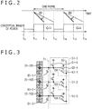
- FIG. 2 A relationship between the number of readouts and the power consumption will next be described with reference to FIG. 2 .
- the image sensor needs to read out all data within one frame, power consumption increases during a readout operation, and it is normal to exercise control to suppress the power consumption in a blank period after the readout.
- reducing the number of readouts contributes to reducing power consumption.
- pixel signal summation is performed and a collective readout is performed, thereby reducing the number of readouts.
- summation there are several variations including FD (floating diffusion) summation between the shared pixels 31, capacity summation between adjacent the VSLs (vertical signal lines), and source follower summation.
- summation is basically limited to that within the shared pixels 31 or that between the adjacent shared pixels 31. Owing to this, at a time of performing imaging with a resolution greatly reduced relative to the number of pixels of the image sensor itself, there is a limit to power reduction since reduction in the number of readouts is limited even using these pixel summation schemes.
- a pixel arrangement such that as depicted by interconnection lines indicated by dotted lines of FIG. 3 , an FD coupling interconnection line 71 connecting FDs 64 for the shared pixels 31 is provided, switches 81-1 to 81-3 for connecting the FD coupling interconnection line 71 are disposed between the rows of the shared pixels 31, and a combination of turning on/off of the switches 81 is changed in response to a necessary resolution to make it possible to reduce the number of readouts.
- the shared pixels 31-101 to 31-103 each of which is configured with eight pixels in total, that is, two sets of configurations of two pixels ⁇ two pixels in a Bayer array that are connected in the vertical direction, are connected to the same vertical signal line 32, and pixel circuits 51-1 to 51-3 are provided to correspond to the shared pixels 31-101 to 31-103, respectively.
- the pixel circuit 51-1 includes a reset (RST) transistor 61-1, an amplification transistor 62-1, a selection (SEL) transistor 63-1, and the FD 64-1.
- reference characters such as the reset (RST) transistor 61-1, the amplification transistor 62-1, the selection (SEL) transistor 63-1, and the FD 64-1, are added only in the pixel circuit 51-1 in FIG. 3 , reference characters are omitted in the other pixel circuits 51, and the reference characters will be also omitted as needed, hereinafter.
- the RST transistor 61 is a transistor that is turned on or off at a time of resetting a photodiode of each pixel or at a time of resetting the FD 64.
- the amplification transistor 62 has a gate to which the FD 64 is connected, amplifies a reference potential or a signal potential at the FD 64, and outputs the amplified reference potential or signal potential to the selection (SEL) transistor 63 as a pixel signal.
- the selection (SEL) transistor 63 is turned on or off on the basis of a selection signal SEL, outputs and transfers the pixel signal amplified by the amplification transistor 62 to the vertical signal line 32.
- the photodiode and a transfer (TRG) transistor are provided in each of the eight pixels in the shared pixels 31.
- the transfer (TRG) transistor is turned on or off in response to turning on or off of the reset (RST) transistor, and resets the photodiode or transfers a charge accumulated in the photodiode to the FD 64.
- RST reset
- each pixel circuit 51 of FIG. 3 is configured with the four transistors described above, the pixel circuit 51 may have a configuration other than that of FIG. 3 , for example, may be configured with the three transistors without the transfer (TRG) transistor.
- each of the pixel circuits 51-2 and 51-3 has a similar configuration.
- switches 81-1 to 81-3 are provided in the FD coupling interconnection line 71 to couple the FDs 64-1 to 64-3 for the shared pixels 31-101 to 31-103 to the FD coupling interconnection line 71, and the FDs 64-1 to 64-3 are coupled to the FD coupling interconnection line 71 by turning on or off the switches 81-1 to 81-3.
- the vertical transfer control section 43 generates control signals such as a transfer signal TRG, a reset signal RST, and the selection signal SEL for exercising control to turn on or off each transfer (TRG) transistor, each reset (RST) transistor 51, and each selection transistor 53, and controls each pixel circuit 51 to operate in each row on the basis of these control signals.
- control signals such as a transfer signal TRG, a reset signal RST, and the selection signal SEL for exercising control to turn on or off each transfer (TRG) transistor, each reset (RST) transistor 51, and each selection transistor 53, and controls each pixel circuit 51 to operate in each row on the basis of these control signals.
- FIG. 4 An example of a configuration of the image sensor 1 in the present disclosure will next be described with reference to FIG. 4 . It is noted that configurations identical in function to those in FIG. 3 are denoted by the same names and the same reference characters and description thereof will be omitted as appropriate. It is noted, however, that in FIG. 4 , the shared pixels 31 are shared pixels 31-121 to 31-126 and the pixel circuits 51 are pixel circuits 51-11 to 51-16. In addition, the FDs 64 in the pixel circuits 51-11 to 51-16 are FDs 64-11 to 64-16. In other words, in FIG. 4 , even the configurations identical in function to those in FIG. 3 are denoted by different reference characters after "-.”
- FIG. 4 differs from that in FIG. 3 in that floating interconnection lines 101-1 to 101-3 sharing the FDs 64 with a predetermined number of shared pixels 31 assumed as a unit and switches 121-1 to 121-6 are provided as an alternative to the common FD coupling interconnection line 71 and the switches 81 changing over the coupling.
- the floating interconnection line 101-2 couples the three FDs 64-13 to 64-15 for the shared pixels 31-123 to 31-125 by changing over the FDs 64-13 to 64-15 by turning on or off the switches 121-3 to 121-5.
- FIG. 4 illustrates an example of the floating interconnection lines 101 in a case in which the maximum number of shared (coupled) FDs 64 is three
- each floating interconnection line 101 may be configured such that the maximum number of FDs 64 coupled to the floating interconnection line 101 is other than three.
- the switches 121 are provided to correspond to the maximum number of coupled FDs 64.
- each floating interconnection line 101 is not directly connected to the FDs 64 but connected to the FDs 64 via the switches 121. Owing to this, a plurality of FDs 64 is connected to the floating interconnection line 101 by turning on or off the switches 121 in response to a necessary resolution, and FD summation by a predetermined number of FDs 64 for a predetermined number of shared pixels 31 is realized.
- a dummy RST transistor is normally provided to ensure layout symmetry of each reset (RST) transistor 61.
- This dummy RST transistor as each switch 121 changing over between connection and disconnection of each FD 64 to and from the floating interconnection line 101 makes it possible to realize a function of coupling the FD 64 to the floating interconnection line 101 without additionally providing elements in each pixel and increasing an interconnection line parasitic capacity for the FD 64.
- a region that configures the FDs 64 subjected to FD summation is configured to be minimized, compared with the conventional image sensor depicted in FIG. 3 .
- adding the floating interconnection lines 101 for the FD summation enables connection of the FD 64 for the pixels for which it is desired to shrink a resolution to the floating interconnection line 101 for FD summation, thereby making it possible to realize the FD summation in response to the resolution.
- the floating interconnection lines 101 for summation can be disconnected at brakes of the pixels after shrinkage.
- FIG. 4 An operation performed when the image sensor 1 in the present disclosure depicted in FIG. 4 captures an image at a low resolution will next be described with reference to a timing chart of FIG. 5 .
- this operation is similar to a readout operation performed in each pixel circuit 51 configured with the four basic transistors except that the switch 121 configured with the dummy RST transistor for the pixels to be subjected to summation is always turned on for realizing the FD summation.
- a waveform of a control signal that is supplied from the vertical transfer control section 43 to each switch 121, which is indicated by the dummy RST transistor (DummyRST[1:n]), and that controls the switch 121 to be turned on or off (signal controlling the switch 121 to be turned on or off) is depicted in an uppermost stage of FIG. 5 .
- a waveform of the selection signal SEL[1:n] supplied from the vertical transfer control section 43 to each selection transistor 53 is depicted in a second stage from the top.
- a waveform of the reset signal RST[1:n] supplied from the vertical transfer control section 43 to each reset (RST) transistor 52 is depicted in a third stage from the top.
- a waveform of the transfer signal TRG[1:n] supplied from the vertical transfer control section 43 to each transfer (TRG) transistor in each pixel in the shared pixel 31 is depicted in a fourth stage from the top. Furthermore, a waveform indicating timing of AD conversion is depicted in a lowermost stage.
- [1:n] indicates herein an identifier for discriminating the waveforms in rows from one another and represents herein that the rows are all the rows from the first to the n-th rows.
- each switch 121 configured with the dummy RST transistor for the pixels to be subjected to summation in response to the resolution is turned on, on the basis of the control signal from the vertical transfer control section 43 for controlling the switch 121 to be turned on or off, and the FDs 64-13 to 64-15 for the shared pixels 31-123 to 31-125 are connected together via the floating interconnection line 101-2, and the selection transistors 63 are all turned on at the same time. While an example of turning on the switches 121 in all rows is depicted in FIG. 5 , the number of the switches 121 turned on and positions of the switches 121 vary depending on the resolution.
- each reset (RST) transistor 61 is turned on to reset the FD 64 on the basis of the reset signal RST from the vertical transfer control section 43 from time t0 to t1, the reference potential is read.
- this reference potential is subjected to AD conversion at timing of time t2 to t3.
- the transfer (TRG) transistor when the transfer (TRG) transistor is turned on, on the basis of the transfer signal TRG from the vertical transfer control section 43 for controlling the transfer (TRG) transistor to be turned on or off to transfer the signal potential to the FD 64 from time t4 to t5, this signal potential is subjected to AD conversion at timing from time t6 to t7.
- the image sensor 1 in the present disclosure has been described with reference to the example of a so-called stacked image sensor configured such that the upper chip 11 on which the pixel array 21 is provided and the lower chip 12 on which the other configurations are provided are stacked
- the image sensor 1 may have another configuration, for example, a configuration such that all the configurations are disposed on the same chip or a configuration such that configured with the two chips and the two chips are not stacked.
- the deterioration in the transfer characteristics and the like due to the power supply drop may be reduced by slightly staggering timing of turning on the reset (RST) transistors and timing of turning on the transfer (TRG) transistors among the rows, as depicted in FIG. 6 .
- the vertical transfer control section 43 outputs the control signal (reset signal RST that is a pulse signal) for turning on the reset (RST) transistors 61 from time t01 to t11 for the first row, but outputs the control signal (reset signal RST that is the pulse signal) from time t02 slightly delayed behind the time t01 to time t12 for the second row.
- control is exercised to output the control signal from slightly delayed time t03 to time t13 and so on for each of the third and the following rows.
- the vertical transfer control section 43 outputs the control signal (transfer signal TRG that is a pulse signal) for turning on the transfer (TRG) transistors from time t41 to t51 for the first row, but outputs the control signal (transfer signal TRG that is the pulse signal) from time t42 slightly delayed behind the time t41 to time t52 for the second row.
- control is exercised to output the control signal from slightly delayed time t43 to time t53 and so on for each of the third and the following rows.
- the FDs 64 for the shared pixels 31 that are a combination of pixels having different exposure time based on so-called HDR (High Dynamic Range) may be connected to the common floating interconnection lines 101.
- HDR High Dynamic Range
- each set of three shared pixels such as shared pixels 31-123 to 31-125, may be changed over between a connected state and a disconnected state by turning on or off the switches 121-3 to 121-5 on the same floating interconnection line 101-2.
- a set of four shared pixels 31-122 to 31-125 may be changed over between the connected state and the disconnected state by turning on or off the switches 121-2 to 121-5 on the same floating interconnection line 101-11.
- the number of shared FDs 64 on the floating interconnection line 101 can be arbitrarily set as long as the number is made uniform.
- the number of the pixels subjected to the long exposure (L) differs from the number of the pixels subjected to the short exposure (S)
- keeping the pixels subjected to the long exposure (L) and the pixels subjected to the short exposure (S) in balance makes it possible to reduce the power consumption related to corrections or the like for an imbalance.
- the floating interconnection lines 101 may be set to straddle the columns.
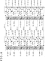
- floating interconnection lines 151 (151-1 to 151-7) connecting the adjacent columns are provided in addition to floating interconnection lines 101-1-1 to 101-3-1 and 101-1-2 to 101-3-2 in the vertical direction as in FIG. 4 .
- Such a configuration can realize shrinkage of the rows in the vertical direction and shrinkage of the columns in the horizontal direction, substantially thin out signals transferred on the vertical signal lines, and reduce the number of the column AD circuits to be used, thereby making it possible to reduce the power consumption at the time of the low resolution.
- Switches changing over between the connected state and the disconnected state to and from the FDs 64 may be provided for the floating interconnection lines 151 in FIG. 8 so that the floating interconnection lines 121 in a column direction can be changed over between the connected state and the disconnected state.
- the image sensor 1 described above can be applied to various kinds of electronic apparatuses, for example, an imaging apparatus such as a digital still camera and a digital video camera, a cellular telephone equipped with an imaging function, or other apparatuses equipped with the imaging function.
- an imaging apparatus such as a digital still camera and a digital video camera
- a cellular telephone equipped with an imaging function or other apparatuses equipped with the imaging function.
- FIG. 9 is a block diagram illustrating an example of a configuration of an imaging apparatus as an electronic apparatus to which the present technique is applied.
- An imaging apparatus 201 depicted in FIG. 9 is configured with an optical system 202, a shutter device 203, a solid-state imaging device 204, a drive circuit 205, a signal processing circuit 206, a monitor 207, and a memory 208, and can capture a still image and a moving image.
- the optical system 202 is configured with one or a plurality of lenses, guides light from a subject (incident light) to the solid-state imaging device 204, and forms an image on a light-receiving surface of the solid-state imaging device 204.
- the shutter device 203 is disposed between the optical system 202 and the solid-state imaging device 204 and controls a light irradiation period and a light shielding period for the solid-state imaging device 204 in accordance with control of the drive circuit 1005.
- the solid-state imaging device 204 is configured with a package including the solid-state imaging device described above.
- the solid-state imaging device 204 accumulates a signal charge for a certain period in response to the light imaged on the light-receiving surface via the optical system 202 and the shutter device 203.
- the signal charge accumulated in the solid-state imaging device 204 is transferred in accordance with a drive signal (timing signal) supplied from the drive circuit 205.
- the drive circuit 205 outputs drive signals for controlling a transfer operation performed by the solid-state imaging device 204 and a shutter operation performed by the shutter device 203 to drive the solid-state imaging device 204 and the shutter device 203.
- the signal processing circuit 206 performs various signal processes on the signal charge output from the solid-state imaging device 204.
- An image (image data) obtained by the signal processes performed by the signal processing circuit 206 is supplied to and displayed on the monitor 207 or supplied to and stored (recorded) in the memory 208.
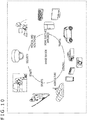
- FIG. 10 is a diagram illustrating a usage example of using the image sensor 1 in FIG. 1 described above.
- a camera module described above can be used in various cases of sensing light such as visible light, infrared light, ultraviolet light, and X-ray as illustrated, for example, below.
Landscapes
- Engineering & Computer Science (AREA)
- Multimedia (AREA)
- Signal Processing (AREA)
- Transforming Light Signals Into Electric Signals (AREA)
- Solid State Image Pick-Up Elements (AREA)
- Color Television Image Signal Generators (AREA)
Applications Claiming Priority (2)
| Application Number | Priority Date | Filing Date | Title |
|---|---|---|---|
| JP2016139999 | 2016-07-15 | ||
| PCT/JP2017/024104 WO2018012316A1 (ja) | 2016-07-15 | 2017-06-30 | 固体撮像素子および固体撮像素子の動作方法、撮像装置、並びに電子機器 |
Publications (3)
| Publication Number | Publication Date |
|---|---|
| EP3487166A4 EP3487166A4 (de) | 2019-05-22 |
| EP3487166A1 true EP3487166A1 (de) | 2019-05-22 |
| EP3487166B1 EP3487166B1 (de) | 2022-01-05 |
Family
ID=60952417
Family Applications (1)
| Application Number | Title | Priority Date | Filing Date |
|---|---|---|---|
| EP17827446.0A Active EP3487166B1 (de) | 2016-07-15 | 2017-06-30 | Festkörperbildgebungselement, verfahren zum betrieb des festkörperbildgebungselements, bildgebungsvorrichtung und elektronische vorrichtung |
Country Status (5)
| Country | Link |
|---|---|
| US (1) | US20190238764A1 (de) |
| EP (1) | EP3487166B1 (de) |
| JP (1) | JP7005493B2 (de) |
| CN (1) | CN109479104B (de) |
| WO (1) | WO2018012316A1 (de) |
Cited By (2)
| Publication number | Priority date | Publication date | Assignee | Title |
|---|---|---|---|---|
| WO2021102366A1 (en) * | 2019-11-20 | 2021-05-27 | Gigajot Technology, Inc. | Scalable-pixel-size image sensor |
| WO2021181734A1 (en) * | 2020-03-13 | 2021-09-16 | Sony Semiconductor Solutions Corporation | Solid-state image capturing element and electronic device |
Families Citing this family (2)
| Publication number | Priority date | Publication date | Assignee | Title |
|---|---|---|---|---|
| US11683609B2 (en) | 2021-07-22 | 2023-06-20 | Samsung Electronics Co., Ltd. | Amplifier circuit for enabling power efficient and faster pixel settling in image sensors |
| JP2024004796A (ja) * | 2022-06-29 | 2024-01-17 | キヤノン株式会社 | 光電変換装置、光電変換システム |
Family Cites Families (20)
| Publication number | Priority date | Publication date | Assignee | Title |
|---|---|---|---|---|
| US7705900B2 (en) * | 2005-06-01 | 2010-04-27 | Eastman Kodak Company | CMOS image sensor pixel with selectable binning and conversion gain |
| US8913166B2 (en) * | 2009-01-21 | 2014-12-16 | Canon Kabushiki Kaisha | Solid-state imaging apparatus |
| JP5267867B2 (ja) * | 2009-03-06 | 2013-08-21 | ルネサスエレクトロニクス株式会社 | 撮像装置 |
| JP5627244B2 (ja) * | 2010-02-08 | 2014-11-19 | キヤノン株式会社 | 固体撮像素子及びその駆動方法及び撮像装置 |
| TWI465716B (zh) * | 2010-06-30 | 2014-12-21 | 生命技術公司 | 用於檢測及測量化學反應及化合物之電晶體電路 |
| JP5885403B2 (ja) * | 2011-06-08 | 2016-03-15 | キヤノン株式会社 | 撮像装置 |
| JP5686765B2 (ja) * | 2011-07-21 | 2015-03-18 | キヤノン株式会社 | 撮像装置およびその制御方法 |
| JP5794686B2 (ja) * | 2011-08-10 | 2015-10-14 | キヤノン株式会社 | 撮像装置及びその駆動方法 |
| JP2013066140A (ja) * | 2011-08-31 | 2013-04-11 | Sony Corp | 撮像装置、および信号処理方法、並びにプログラム |
| JP5915031B2 (ja) * | 2011-08-31 | 2016-05-11 | ソニー株式会社 | 撮像装置および撮像方法、並びに電子機器 |
| JP2015039086A (ja) * | 2011-12-16 | 2015-02-26 | パナソニック株式会社 | 固体撮像装置、撮像装置 |
| JP5895525B2 (ja) | 2011-12-28 | 2016-03-30 | 株式会社ニコン | 撮像素子 |
| JP5958740B2 (ja) * | 2012-03-06 | 2016-08-02 | ソニー株式会社 | 固体撮像素子および駆動方法、並びに、電子機器 |
| US9420208B2 (en) * | 2012-07-13 | 2016-08-16 | Canon Kabushiki Kaisha | Driving method for image pickup apparatus and driving method for image pickup system |
| JP6639385B2 (ja) * | 2013-06-11 | 2020-02-05 | ラムバス・インコーポレーテッド | スプリットゲート条件付きリセットイメージセンサ |
| JP6239975B2 (ja) * | 2013-12-27 | 2017-11-29 | キヤノン株式会社 | 固体撮像装置及びそれを用いた撮像システム |
| US9686485B2 (en) * | 2014-05-30 | 2017-06-20 | Apple Inc. | Pixel binning in an image sensor |
| WO2016013413A1 (ja) * | 2014-07-25 | 2016-01-28 | ソニー株式会社 | 固体撮像素子、ad変換器、および電子機器 |
| JP6670451B2 (ja) * | 2014-10-01 | 2020-03-25 | ソニー株式会社 | 固体撮像装置、信号処理方法、及び、電子機器 |
| JP2016111425A (ja) * | 2014-12-03 | 2016-06-20 | ルネサスエレクトロニクス株式会社 | 撮像装置 |
-
2017
- 2017-06-30 WO PCT/JP2017/024104 patent/WO2018012316A1/ja not_active Ceased
- 2017-06-30 JP JP2018527515A patent/JP7005493B2/ja active Active
- 2017-06-30 CN CN201780042516.4A patent/CN109479104B/zh active Active
- 2017-06-30 EP EP17827446.0A patent/EP3487166B1/de active Active
- 2017-06-30 US US16/318,100 patent/US20190238764A1/en not_active Abandoned
Cited By (6)
| Publication number | Priority date | Publication date | Assignee | Title |
|---|---|---|---|---|
| WO2021102366A1 (en) * | 2019-11-20 | 2021-05-27 | Gigajot Technology, Inc. | Scalable-pixel-size image sensor |
| US11114482B2 (en) | 2019-11-20 | 2021-09-07 | Gigajot Technology, Inc. | Scalable-pixel-size image sensor |
| US11721708B2 (en) | 2019-11-20 | 2023-08-08 | Gigajot Technologies, Inc. | Scalable-pixel-size image sensor |
| US11721707B2 (en) | 2019-11-20 | 2023-08-08 | Gigajot Technologies, Inc. | Scalable-pixel-size image sensor |
| WO2021181734A1 (en) * | 2020-03-13 | 2021-09-16 | Sony Semiconductor Solutions Corporation | Solid-state image capturing element and electronic device |
| US11653122B2 (en) | 2020-03-13 | 2023-05-16 | Sony Semiconductor Solutions Corporation | Solid-state image capturing element with floating diffusion layers processing a signal undergoing pixel addition |
Also Published As
| Publication number | Publication date |
|---|---|
| US20190238764A1 (en) | 2019-08-01 |
| CN109479104B (zh) | 2022-02-18 |
| EP3487166A4 (de) | 2019-05-22 |
| EP3487166B1 (de) | 2022-01-05 |
| CN109479104A (zh) | 2019-03-15 |
| JPWO2018012316A1 (ja) | 2019-04-25 |
| JP7005493B2 (ja) | 2022-01-21 |
| WO2018012316A1 (ja) | 2018-01-18 |
Similar Documents
| Publication | Publication Date | Title |
|---|---|---|
| US10811447B2 (en) | Solid-state imaging device, driving method, and electronic equipment | |
| US10741605B2 (en) | Solid-state image sensor, imaging device, and electronic equipment | |
| US10798318B2 (en) | Solid-state imaging element, imaging device, and electronic device | |
| US11743619B2 (en) | Solid-state imaging element and electronic device including a shared structure for pixels for sharing an AD converter | |
| EP3487166B1 (de) | Festkörperbildgebungselement, verfahren zum betrieb des festkörperbildgebungselements, bildgebungsvorrichtung und elektronische vorrichtung | |
| US20090046187A1 (en) | Solid-state imaging device | |
| US10602088B2 (en) | Solid-state imaging device and imaging apparatus | |
| JP2017076872A (ja) | 撮像素子 | |
| US10848700B2 (en) | Imaging device with switch circuit | |
| US11910117B2 (en) | Solid-state imaging element and electronic apparatus | |
| US10547806B2 (en) | Solid-state imaging element, method for operating solid-state imaging element, imaging device, and electronic equipment | |
| WO2026074907A1 (ja) | 光検出装置および電子機器 |
Legal Events
| Date | Code | Title | Description |
|---|---|---|---|
| STAA | Information on the status of an ep patent application or granted ep patent |
Free format text: STATUS: THE INTERNATIONAL PUBLICATION HAS BEEN MADE |
|
| PUAI | Public reference made under article 153(3) epc to a published international application that has entered the european phase |
Free format text: ORIGINAL CODE: 0009012 |
|
| STAA | Information on the status of an ep patent application or granted ep patent |
Free format text: STATUS: REQUEST FOR EXAMINATION WAS MADE |
|
| 17P | Request for examination filed |
Effective date: 20190211 |
|
| A4 | Supplementary search report drawn up and despatched |
Effective date: 20190408 |
|
| AK | Designated contracting states |
Kind code of ref document: A1 Designated state(s): AL AT BE BG CH CY CZ DE DK EE ES FI FR GB GR HR HU IE IS IT LI LT LU LV MC MK MT NL NO PL PT RO RS SE SI SK SM TR |
|
| AX | Request for extension of the european patent |
Extension state: BA ME |
|
| DAV | Request for validation of the european patent (deleted) | ||
| DAX | Request for extension of the european patent (deleted) | ||
| STAA | Information on the status of an ep patent application or granted ep patent |
Free format text: STATUS: EXAMINATION IS IN PROGRESS |
|
| 17Q | First examination report despatched |
Effective date: 20200623 |
|
| GRAP | Despatch of communication of intention to grant a patent |
Free format text: ORIGINAL CODE: EPIDOSNIGR1 |
|
| STAA | Information on the status of an ep patent application or granted ep patent |
Free format text: STATUS: GRANT OF PATENT IS INTENDED |
|
| INTG | Intention to grant announced |
Effective date: 20210728 |
|
| GRAS | Grant fee paid |
Free format text: ORIGINAL CODE: EPIDOSNIGR3 |
|
| GRAA | (expected) grant |
Free format text: ORIGINAL CODE: 0009210 |
|
| STAA | Information on the status of an ep patent application or granted ep patent |
Free format text: STATUS: THE PATENT HAS BEEN GRANTED |
|
| AK | Designated contracting states |
Kind code of ref document: B1 Designated state(s): AL AT BE BG CH CY CZ DE DK EE ES FI FR GB GR HR HU IE IS IT LI LT LU LV MC MK MT NL NO PL PT RO RS SE SI SK SM TR |
|
| REG | Reference to a national code |
Ref country code: GB Ref legal event code: FG4D |
|
| REG | Reference to a national code |
Ref country code: CH Ref legal event code: EP |
|
| REG | Reference to a national code |
Ref country code: AT Ref legal event code: REF Ref document number: 1461625 Country of ref document: AT Kind code of ref document: T Effective date: 20220115 |
|
| REG | Reference to a national code |
Ref country code: DE Ref legal event code: R096 Ref document number: 602017051998 Country of ref document: DE |
|
| REG | Reference to a national code |
Ref country code: IE Ref legal event code: FG4D |
|
| REG | Reference to a national code |
Ref country code: LT Ref legal event code: MG9D |
|
| REG | Reference to a national code |
Ref country code: NL Ref legal event code: MP Effective date: 20220105 |
|
| REG | Reference to a national code |
Ref country code: AT Ref legal event code: MK05 Ref document number: 1461625 Country of ref document: AT Kind code of ref document: T Effective date: 20220105 |
|
| PG25 | Lapsed in a contracting state [announced via postgrant information from national office to epo] |
Ref country code: NL Free format text: LAPSE BECAUSE OF FAILURE TO SUBMIT A TRANSLATION OF THE DESCRIPTION OR TO PAY THE FEE WITHIN THE PRESCRIBED TIME-LIMIT Effective date: 20220105 |
|
| PG25 | Lapsed in a contracting state [announced via postgrant information from national office to epo] |
Ref country code: SE Free format text: LAPSE BECAUSE OF FAILURE TO SUBMIT A TRANSLATION OF THE DESCRIPTION OR TO PAY THE FEE WITHIN THE PRESCRIBED TIME-LIMIT Effective date: 20220105 Ref country code: RS Free format text: LAPSE BECAUSE OF FAILURE TO SUBMIT A TRANSLATION OF THE DESCRIPTION OR TO PAY THE FEE WITHIN THE PRESCRIBED TIME-LIMIT Effective date: 20220105 Ref country code: PT Free format text: LAPSE BECAUSE OF FAILURE TO SUBMIT A TRANSLATION OF THE DESCRIPTION OR TO PAY THE FEE WITHIN THE PRESCRIBED TIME-LIMIT Effective date: 20220505 Ref country code: NO Free format text: LAPSE BECAUSE OF FAILURE TO SUBMIT A TRANSLATION OF THE DESCRIPTION OR TO PAY THE FEE WITHIN THE PRESCRIBED TIME-LIMIT Effective date: 20220405 Ref country code: LT Free format text: LAPSE BECAUSE OF FAILURE TO SUBMIT A TRANSLATION OF THE DESCRIPTION OR TO PAY THE FEE WITHIN THE PRESCRIBED TIME-LIMIT Effective date: 20220105 Ref country code: HR Free format text: LAPSE BECAUSE OF FAILURE TO SUBMIT A TRANSLATION OF THE DESCRIPTION OR TO PAY THE FEE WITHIN THE PRESCRIBED TIME-LIMIT Effective date: 20220105 Ref country code: ES Free format text: LAPSE BECAUSE OF FAILURE TO SUBMIT A TRANSLATION OF THE DESCRIPTION OR TO PAY THE FEE WITHIN THE PRESCRIBED TIME-LIMIT Effective date: 20220105 Ref country code: BG Free format text: LAPSE BECAUSE OF FAILURE TO SUBMIT A TRANSLATION OF THE DESCRIPTION OR TO PAY THE FEE WITHIN THE PRESCRIBED TIME-LIMIT Effective date: 20220405 |
|
| PG25 | Lapsed in a contracting state [announced via postgrant information from national office to epo] |
Ref country code: PL Free format text: LAPSE BECAUSE OF FAILURE TO SUBMIT A TRANSLATION OF THE DESCRIPTION OR TO PAY THE FEE WITHIN THE PRESCRIBED TIME-LIMIT Effective date: 20220105 Ref country code: LV Free format text: LAPSE BECAUSE OF FAILURE TO SUBMIT A TRANSLATION OF THE DESCRIPTION OR TO PAY THE FEE WITHIN THE PRESCRIBED TIME-LIMIT Effective date: 20220105 Ref country code: GR Free format text: LAPSE BECAUSE OF FAILURE TO SUBMIT A TRANSLATION OF THE DESCRIPTION OR TO PAY THE FEE WITHIN THE PRESCRIBED TIME-LIMIT Effective date: 20220406 Ref country code: FI Free format text: LAPSE BECAUSE OF FAILURE TO SUBMIT A TRANSLATION OF THE DESCRIPTION OR TO PAY THE FEE WITHIN THE PRESCRIBED TIME-LIMIT Effective date: 20220105 Ref country code: AT Free format text: LAPSE BECAUSE OF FAILURE TO SUBMIT A TRANSLATION OF THE DESCRIPTION OR TO PAY THE FEE WITHIN THE PRESCRIBED TIME-LIMIT Effective date: 20220105 |
|
| PG25 | Lapsed in a contracting state [announced via postgrant information from national office to epo] |
Ref country code: IS Free format text: LAPSE BECAUSE OF FAILURE TO SUBMIT A TRANSLATION OF THE DESCRIPTION OR TO PAY THE FEE WITHIN THE PRESCRIBED TIME-LIMIT Effective date: 20220505 |
|
| REG | Reference to a national code |
Ref country code: DE Ref legal event code: R097 Ref document number: 602017051998 Country of ref document: DE |
|
| PG25 | Lapsed in a contracting state [announced via postgrant information from national office to epo] |
Ref country code: SM Free format text: LAPSE BECAUSE OF FAILURE TO SUBMIT A TRANSLATION OF THE DESCRIPTION OR TO PAY THE FEE WITHIN THE PRESCRIBED TIME-LIMIT Effective date: 20220105 Ref country code: SK Free format text: LAPSE BECAUSE OF FAILURE TO SUBMIT A TRANSLATION OF THE DESCRIPTION OR TO PAY THE FEE WITHIN THE PRESCRIBED TIME-LIMIT Effective date: 20220105 Ref country code: RO Free format text: LAPSE BECAUSE OF FAILURE TO SUBMIT A TRANSLATION OF THE DESCRIPTION OR TO PAY THE FEE WITHIN THE PRESCRIBED TIME-LIMIT Effective date: 20220105 Ref country code: EE Free format text: LAPSE BECAUSE OF FAILURE TO SUBMIT A TRANSLATION OF THE DESCRIPTION OR TO PAY THE FEE WITHIN THE PRESCRIBED TIME-LIMIT Effective date: 20220105 Ref country code: DK Free format text: LAPSE BECAUSE OF FAILURE TO SUBMIT A TRANSLATION OF THE DESCRIPTION OR TO PAY THE FEE WITHIN THE PRESCRIBED TIME-LIMIT Effective date: 20220105 Ref country code: CZ Free format text: LAPSE BECAUSE OF FAILURE TO SUBMIT A TRANSLATION OF THE DESCRIPTION OR TO PAY THE FEE WITHIN THE PRESCRIBED TIME-LIMIT Effective date: 20220105 |
|
| PLBE | No opposition filed within time limit |
Free format text: ORIGINAL CODE: 0009261 |
|
| STAA | Information on the status of an ep patent application or granted ep patent |
Free format text: STATUS: NO OPPOSITION FILED WITHIN TIME LIMIT |
|
| REG | Reference to a national code |
Ref country code: DE Ref legal event code: R079 Ref document number: 602017051998 Country of ref document: DE Free format text: PREVIOUS MAIN CLASS: H04N0005374500 Ipc: H04N0025770000 |
|
| PG25 | Lapsed in a contracting state [announced via postgrant information from national office to epo] |
Ref country code: AL Free format text: LAPSE BECAUSE OF FAILURE TO SUBMIT A TRANSLATION OF THE DESCRIPTION OR TO PAY THE FEE WITHIN THE PRESCRIBED TIME-LIMIT Effective date: 20220105 |
|
| 26N | No opposition filed |
Effective date: 20221006 |
|
| PG25 | Lapsed in a contracting state [announced via postgrant information from national office to epo] |
Ref country code: MC Free format text: LAPSE BECAUSE OF FAILURE TO SUBMIT A TRANSLATION OF THE DESCRIPTION OR TO PAY THE FEE WITHIN THE PRESCRIBED TIME-LIMIT Effective date: 20220105 |
|
| REG | Reference to a national code |
Ref country code: CH Ref legal event code: PL |
|
| REG | Reference to a national code |
Ref country code: BE Ref legal event code: MM Effective date: 20220630 |
|
| PG25 | Lapsed in a contracting state [announced via postgrant information from national office to epo] |
Ref country code: SI Free format text: LAPSE BECAUSE OF FAILURE TO SUBMIT A TRANSLATION OF THE DESCRIPTION OR TO PAY THE FEE WITHIN THE PRESCRIBED TIME-LIMIT Effective date: 20220105 |
|
| GBPC | Gb: european patent ceased through non-payment of renewal fee |
Effective date: 20220630 |
|
| PG25 | Lapsed in a contracting state [announced via postgrant information from national office to epo] |
Ref country code: LU Free format text: LAPSE BECAUSE OF NON-PAYMENT OF DUE FEES Effective date: 20220630 Ref country code: LI Free format text: LAPSE BECAUSE OF NON-PAYMENT OF DUE FEES Effective date: 20220630 Ref country code: IE Free format text: LAPSE BECAUSE OF NON-PAYMENT OF DUE FEES Effective date: 20220630 Ref country code: FR Free format text: LAPSE BECAUSE OF NON-PAYMENT OF DUE FEES Effective date: 20220630 Ref country code: CH Free format text: LAPSE BECAUSE OF NON-PAYMENT OF DUE FEES Effective date: 20220630 |
|
| PG25 | Lapsed in a contracting state [announced via postgrant information from national office to epo] |
Ref country code: GB Free format text: LAPSE BECAUSE OF NON-PAYMENT OF DUE FEES Effective date: 20220630 Ref country code: BE Free format text: LAPSE BECAUSE OF NON-PAYMENT OF DUE FEES Effective date: 20220630 |
|
| P01 | Opt-out of the competence of the unified patent court (upc) registered |
Effective date: 20230528 |
|
| PG25 | Lapsed in a contracting state [announced via postgrant information from national office to epo] |
Ref country code: IT Free format text: LAPSE BECAUSE OF FAILURE TO SUBMIT A TRANSLATION OF THE DESCRIPTION OR TO PAY THE FEE WITHIN THE PRESCRIBED TIME-LIMIT Effective date: 20220105 |
|
| PG25 | Lapsed in a contracting state [announced via postgrant information from national office to epo] |
Ref country code: HU Free format text: LAPSE BECAUSE OF FAILURE TO SUBMIT A TRANSLATION OF THE DESCRIPTION OR TO PAY THE FEE WITHIN THE PRESCRIBED TIME-LIMIT; INVALID AB INITIO Effective date: 20170630 |
|
| PG25 | Lapsed in a contracting state [announced via postgrant information from national office to epo] |
Ref country code: MK Free format text: LAPSE BECAUSE OF FAILURE TO SUBMIT A TRANSLATION OF THE DESCRIPTION OR TO PAY THE FEE WITHIN THE PRESCRIBED TIME-LIMIT Effective date: 20220105 Ref country code: CY Free format text: LAPSE BECAUSE OF FAILURE TO SUBMIT A TRANSLATION OF THE DESCRIPTION OR TO PAY THE FEE WITHIN THE PRESCRIBED TIME-LIMIT Effective date: 20220105 |
|
| PG25 | Lapsed in a contracting state [announced via postgrant information from national office to epo] |
Ref country code: TR Free format text: LAPSE BECAUSE OF FAILURE TO SUBMIT A TRANSLATION OF THE DESCRIPTION OR TO PAY THE FEE WITHIN THE PRESCRIBED TIME-LIMIT Effective date: 20220105 |
|
| PG25 | Lapsed in a contracting state [announced via postgrant information from national office to epo] |
Ref country code: MT Free format text: LAPSE BECAUSE OF FAILURE TO SUBMIT A TRANSLATION OF THE DESCRIPTION OR TO PAY THE FEE WITHIN THE PRESCRIBED TIME-LIMIT Effective date: 20220105 |
|
| PGFP | Annual fee paid to national office [announced via postgrant information from national office to epo] |
Ref country code: DE Payment date: 20250520 Year of fee payment: 9 |