EP3486940A1 - Herstellungsverfahren für halbleiterlaminierte folie sowie halbleiterlaminierte folie - Google Patents
Herstellungsverfahren für halbleiterlaminierte folie sowie halbleiterlaminierte folie Download PDFInfo
- Publication number
- EP3486940A1 EP3486940A1 EP17827672.1A EP17827672A EP3486940A1 EP 3486940 A1 EP3486940 A1 EP 3486940A1 EP 17827672 A EP17827672 A EP 17827672A EP 3486940 A1 EP3486940 A1 EP 3486940A1
- Authority
- EP
- European Patent Office
- Prior art keywords
- semiconductor layer
- semiconductor
- layer
- less
- laminate film
- Prior art date
- Legal status (The legal status is an assumption and is not a legal conclusion. Google has not performed a legal analysis and makes no representation as to the accuracy of the status listed.)
- Pending
Links
Images




Classifications
-
- H—ELECTRICITY
- H10—SEMICONDUCTOR DEVICES; ELECTRIC SOLID-STATE DEVICES NOT OTHERWISE PROVIDED FOR
- H10P—GENERIC PROCESSES OR APPARATUS FOR THE MANUFACTURE OR TREATMENT OF DEVICES COVERED BY CLASS H10
- H10P14/00—Formation of materials, e.g. in the shape of layers or pillars
- H10P14/20—Formation of materials, e.g. in the shape of layers or pillars of semiconductor materials
- H10P14/29—Formation of materials, e.g. in the shape of layers or pillars of semiconductor materials characterised by the substrates
- H10P14/2901—Materials
- H10P14/2902—Materials being Group IVA materials
- H10P14/2905—Silicon, silicon germanium or germanium
-
- C—CHEMISTRY; METALLURGY
- C23—COATING METALLIC MATERIAL; COATING MATERIAL WITH METALLIC MATERIAL; CHEMICAL SURFACE TREATMENT; DIFFUSION TREATMENT OF METALLIC MATERIAL; COATING BY VACUUM EVAPORATION, BY SPUTTERING, BY ION IMPLANTATION OR BY CHEMICAL VAPOUR DEPOSITION, IN GENERAL; INHIBITING CORROSION OF METALLIC MATERIAL OR INCRUSTATION IN GENERAL
- C23C—COATING METALLIC MATERIAL; COATING MATERIAL WITH METALLIC MATERIAL; SURFACE TREATMENT OF METALLIC MATERIAL BY DIFFUSION INTO THE SURFACE, BY CHEMICAL CONVERSION OR SUBSTITUTION; COATING BY VACUUM EVAPORATION, BY SPUTTERING, BY ION IMPLANTATION OR BY CHEMICAL VAPOUR DEPOSITION, IN GENERAL
- C23C14/00—Coating by vacuum evaporation, by sputtering or by ion implantation of the coating forming material
- C23C14/06—Coating by vacuum evaporation, by sputtering or by ion implantation of the coating forming material characterised by the coating material
-
- C—CHEMISTRY; METALLURGY
- C23—COATING METALLIC MATERIAL; COATING MATERIAL WITH METALLIC MATERIAL; CHEMICAL SURFACE TREATMENT; DIFFUSION TREATMENT OF METALLIC MATERIAL; COATING BY VACUUM EVAPORATION, BY SPUTTERING, BY ION IMPLANTATION OR BY CHEMICAL VAPOUR DEPOSITION, IN GENERAL; INHIBITING CORROSION OF METALLIC MATERIAL OR INCRUSTATION IN GENERAL
- C23C—COATING METALLIC MATERIAL; COATING MATERIAL WITH METALLIC MATERIAL; SURFACE TREATMENT OF METALLIC MATERIAL BY DIFFUSION INTO THE SURFACE, BY CHEMICAL CONVERSION OR SUBSTITUTION; COATING BY VACUUM EVAPORATION, BY SPUTTERING, BY ION IMPLANTATION OR BY CHEMICAL VAPOUR DEPOSITION, IN GENERAL
- C23C14/00—Coating by vacuum evaporation, by sputtering or by ion implantation of the coating forming material
- C23C14/06—Coating by vacuum evaporation, by sputtering or by ion implantation of the coating forming material characterised by the coating material
- C23C14/14—Metallic material, boron or silicon
-
- C—CHEMISTRY; METALLURGY
- C23—COATING METALLIC MATERIAL; COATING MATERIAL WITH METALLIC MATERIAL; CHEMICAL SURFACE TREATMENT; DIFFUSION TREATMENT OF METALLIC MATERIAL; COATING BY VACUUM EVAPORATION, BY SPUTTERING, BY ION IMPLANTATION OR BY CHEMICAL VAPOUR DEPOSITION, IN GENERAL; INHIBITING CORROSION OF METALLIC MATERIAL OR INCRUSTATION IN GENERAL
- C23C—COATING METALLIC MATERIAL; COATING MATERIAL WITH METALLIC MATERIAL; SURFACE TREATMENT OF METALLIC MATERIAL BY DIFFUSION INTO THE SURFACE, BY CHEMICAL CONVERSION OR SUBSTITUTION; COATING BY VACUUM EVAPORATION, BY SPUTTERING, BY ION IMPLANTATION OR BY CHEMICAL VAPOUR DEPOSITION, IN GENERAL
- C23C14/00—Coating by vacuum evaporation, by sputtering or by ion implantation of the coating forming material
- C23C14/06—Coating by vacuum evaporation, by sputtering or by ion implantation of the coating forming material characterised by the coating material
- C23C14/14—Metallic material, boron or silicon
- C23C14/16—Metallic material, boron or silicon on metallic substrates or on substrates of boron or silicon
- C23C14/165—Metallic material, boron or silicon on metallic substrates or on substrates of boron or silicon by cathodic sputtering
-
- C—CHEMISTRY; METALLURGY
- C23—COATING METALLIC MATERIAL; COATING MATERIAL WITH METALLIC MATERIAL; CHEMICAL SURFACE TREATMENT; DIFFUSION TREATMENT OF METALLIC MATERIAL; COATING BY VACUUM EVAPORATION, BY SPUTTERING, BY ION IMPLANTATION OR BY CHEMICAL VAPOUR DEPOSITION, IN GENERAL; INHIBITING CORROSION OF METALLIC MATERIAL OR INCRUSTATION IN GENERAL
- C23C—COATING METALLIC MATERIAL; COATING MATERIAL WITH METALLIC MATERIAL; SURFACE TREATMENT OF METALLIC MATERIAL BY DIFFUSION INTO THE SURFACE, BY CHEMICAL CONVERSION OR SUBSTITUTION; COATING BY VACUUM EVAPORATION, BY SPUTTERING, BY ION IMPLANTATION OR BY CHEMICAL VAPOUR DEPOSITION, IN GENERAL
- C23C14/00—Coating by vacuum evaporation, by sputtering or by ion implantation of the coating forming material
- C23C14/22—Coating by vacuum evaporation, by sputtering or by ion implantation of the coating forming material characterised by the process of coating
- C23C14/34—Sputtering
-
- H—ELECTRICITY
- H10—SEMICONDUCTOR DEVICES; ELECTRIC SOLID-STATE DEVICES NOT OTHERWISE PROVIDED FOR
- H10D—INORGANIC ELECTRIC SEMICONDUCTOR DEVICES
- H10D10/00—Bipolar junction transistors [BJT]
- H10D10/80—Heterojunction BJTs
-
- H—ELECTRICITY
- H10—SEMICONDUCTOR DEVICES; ELECTRIC SOLID-STATE DEVICES NOT OTHERWISE PROVIDED FOR
- H10D—INORGANIC ELECTRIC SEMICONDUCTOR DEVICES
- H10D30/00—Field-effect transistors [FET]
- H10D30/40—FETs having zero-dimensional [0D], one-dimensional [1D] or two-dimensional [2D] charge carrier gas channels
- H10D30/47—FETs having zero-dimensional [0D], one-dimensional [1D] or two-dimensional [2D] charge carrier gas channels having two-dimensional [2D] charge carrier gas channels, e.g. nanoribbon FETs or high electron mobility transistors [HEMT]
-
- H—ELECTRICITY
- H10—SEMICONDUCTOR DEVICES; ELECTRIC SOLID-STATE DEVICES NOT OTHERWISE PROVIDED FOR
- H10D—INORGANIC ELECTRIC SEMICONDUCTOR DEVICES
- H10D30/00—Field-effect transistors [FET]
- H10D30/60—Insulated-gate field-effect transistors [IGFET]
-
- H—ELECTRICITY
- H10—SEMICONDUCTOR DEVICES; ELECTRIC SOLID-STATE DEVICES NOT OTHERWISE PROVIDED FOR
- H10D—INORGANIC ELECTRIC SEMICONDUCTOR DEVICES
- H10D30/00—Field-effect transistors [FET]
- H10D30/80—FETs having rectifying junction gate electrodes
- H10D30/87—FETs having Schottky gate electrodes, e.g. metal-semiconductor FETs [MESFET]
-
- H—ELECTRICITY
- H10—SEMICONDUCTOR DEVICES; ELECTRIC SOLID-STATE DEVICES NOT OTHERWISE PROVIDED FOR
- H10D—INORGANIC ELECTRIC SEMICONDUCTOR DEVICES
- H10D62/00—Semiconductor bodies, or regions thereof, of devices having potential barriers
- H10D62/80—Semiconductor bodies, or regions thereof, of devices having potential barriers characterised by the materials
- H10D62/82—Heterojunctions
- H10D62/822—Heterojunctions comprising only Group IV materials heterojunctions, e.g. Si/Ge heterojunctions
-
- H—ELECTRICITY
- H10—SEMICONDUCTOR DEVICES; ELECTRIC SOLID-STATE DEVICES NOT OTHERWISE PROVIDED FOR
- H10D—INORGANIC ELECTRIC SEMICONDUCTOR DEVICES
- H10D62/00—Semiconductor bodies, or regions thereof, of devices having potential barriers
- H10D62/80—Semiconductor bodies, or regions thereof, of devices having potential barriers characterised by the materials
- H10D62/83—Semiconductor bodies, or regions thereof, of devices having potential barriers characterised by the materials being Group IV materials, e.g. B-doped Si or undoped Ge
- H10D62/832—Semiconductor bodies, or regions thereof, of devices having potential barriers characterised by the materials being Group IV materials, e.g. B-doped Si or undoped Ge being Group IV materials comprising two or more elements, e.g. SiGe
-
- H—ELECTRICITY
- H10—SEMICONDUCTOR DEVICES; ELECTRIC SOLID-STATE DEVICES NOT OTHERWISE PROVIDED FOR
- H10D—INORGANIC ELECTRIC SEMICONDUCTOR DEVICES
- H10D8/00—Diodes
- H10D8/70—Tunnel-effect diodes
-
- H—ELECTRICITY
- H10—SEMICONDUCTOR DEVICES; ELECTRIC SOLID-STATE DEVICES NOT OTHERWISE PROVIDED FOR
- H10P—GENERIC PROCESSES OR APPARATUS FOR THE MANUFACTURE OR TREATMENT OF DEVICES COVERED BY CLASS H10
- H10P14/00—Formation of materials, e.g. in the shape of layers or pillars
- H10P14/20—Formation of materials, e.g. in the shape of layers or pillars of semiconductor materials
-
- H—ELECTRICITY
- H10—SEMICONDUCTOR DEVICES; ELECTRIC SOLID-STATE DEVICES NOT OTHERWISE PROVIDED FOR
- H10P—GENERIC PROCESSES OR APPARATUS FOR THE MANUFACTURE OR TREATMENT OF DEVICES COVERED BY CLASS H10
- H10P14/00—Formation of materials, e.g. in the shape of layers or pillars
- H10P14/20—Formation of materials, e.g. in the shape of layers or pillars of semiconductor materials
- H10P14/22—Formation of materials, e.g. in the shape of layers or pillars of semiconductor materials using physical deposition, e.g. vacuum deposition or sputtering
-
- H—ELECTRICITY
- H10—SEMICONDUCTOR DEVICES; ELECTRIC SOLID-STATE DEVICES NOT OTHERWISE PROVIDED FOR
- H10P—GENERIC PROCESSES OR APPARATUS FOR THE MANUFACTURE OR TREATMENT OF DEVICES COVERED BY CLASS H10
- H10P14/00—Formation of materials, e.g. in the shape of layers or pillars
- H10P14/20—Formation of materials, e.g. in the shape of layers or pillars of semiconductor materials
- H10P14/34—Deposited materials, e.g. layers
- H10P14/3402—Deposited materials, e.g. layers characterised by the chemical composition
- H10P14/3404—Deposited materials, e.g. layers characterised by the chemical composition being Group IVA materials
- H10P14/3411—Silicon, silicon germanium or germanium
-
- H—ELECTRICITY
- H10—SEMICONDUCTOR DEVICES; ELECTRIC SOLID-STATE DEVICES NOT OTHERWISE PROVIDED FOR
- H10D—INORGANIC ELECTRIC SEMICONDUCTOR DEVICES
- H10D30/00—Field-effect transistors [FET]
- H10D30/40—FETs having zero-dimensional [0D], one-dimensional [1D] or two-dimensional [2D] charge carrier gas channels
- H10D30/47—FETs having zero-dimensional [0D], one-dimensional [1D] or two-dimensional [2D] charge carrier gas channels having two-dimensional [2D] charge carrier gas channels, e.g. nanoribbon FETs or high electron mobility transistors [HEMT]
- H10D30/471—High electron mobility transistors [HEMT] or high hole mobility transistors [HHMT]
Definitions
- the present invention relates to a method of producing a semiconductor laminate film, and a semiconductor laminate film.
- HEMTs high electron mobility transistors
- DCFETs doped-channel field-effect transistors
- RTDs resonant tunneling diodes
- HBTs hetero-bipolar transistors
- MOSFETs strained-channel metal-oxide-semiconductor field-effect transistors
- a HEMT using holes as carriers p-HEMT or HHMT
- a DCFET using holes as carriers p-DCFET
- p-RTD hole tunneling RTD
- HBT hetero-bipolar transistor
- MOSFET with a strained SiGe channel using holes as carriers strained-SiGe-channel p-MOSFET
- buried-channel MOSFET using holes as carriers buried-channel p-MOSFET
- the SiGe layer having compressive strain can form a potential well for a hole in a valence band through a change in a band width, to thereby realize a structure for achieving an increase in speed.
- the SiGe layer having compressive strain can increase a mobility (speed) of a hole passing therethrough. Thus, an increase in speed of the device can be achieved.
- the compressive strain of the SiGe layer is increased by increasing a composition ratio of Ge (ratio of the number of Ge atoms) in the SiGe layer, the potential well becomes deeper, and the mobility becomes higher, and thus a device having a higher speed can be achieved.
- Non Patent Literature 1 Journal of Applied Physics, vol. 95, no. 12, June 15, 2004, pp. 7681-7689
- a SiGe layer is formed on a Si substrate by a chemical vapor deposition (CVD) method.
- Patent Literature 1 JP-A-2008-21674
- a SiGe layer is formed on a Si substrate by a sputtering method using a mixed gas containing hydrogen as a sputtering gas.
- the inventors of the invention have focused attention on a sputtering method in order to form a SiGe layer having large compressive strain capable of sufficiently improving the characteristics of a semiconductor device, and have made extensive investigations on various film formation conditions.
- a substrate temperature at the time of formation of the SiGe layer film formation temperature
- the concentration of hydrogen in a sputtering gas at the time of formation of the SiGe layer and the pressure of the sputtering gas at the time of formation of the SiGe layer (film formation pressure) are particularly important.
- An objective of the invention is to provide a method of producing a semiconductor laminate film capable of growing a semiconductor layer containing silicon and germanium so as to be better lattice-matched with a silicon substrate even when the semiconductor layer has a high composition ratio of germanium, to thereby produce a semiconductor device having satisfactory characteristics.
- Another objective of the invention is to provide a semiconductor laminate film which includes a semiconductor layer containing silicon and germanium which is better lattice-matched with a silicon substrate even when the semiconductor layer has a high composition ratio of germanium, and is thus capable of producing a semiconductor device having satisfactory characteristics.
- a method of producing a semiconductor laminate film including forming a semiconductor layer containing silicon and germanium on a silicon substrate by a sputtering method, in the sputtering method, a film formation temperature of the semiconductor layer being less than 500 °C, and a film formation pressure of the semiconductor layer ranging from 1 mTorr to 11 mTorr, or, a film formation temperature of the semiconductor layer being less than 600 °C, and a film formation pressure of the semiconductor layer being equal to or more than 2 mTorr and less than 5 mTorr, the sputtering method using a sputtering gas having a volume ratio of a hydrogen gas of less than 0.1%, and the semiconductor layer satisfying a following relationship t ⁇ 0 ⁇ .881 ⁇ x ⁇ 4.79 where t represents a thickness (nm) of the semiconductor layer, and x represents a ratio of the number of germanium atoms to a sum of the number of
- the semiconductor layer having larger compressive strain i.e., a lower lattice mismatch rate f
- a semiconductor layer formed under the film formation conditions of, for example, a volume ratio of a hydrogen gas in the sputtering gas of 0.1% or more can be formed (the details are described later).
- the semiconductor layer can be grown so as to be better lattice-matched with the silicon substrate even when the semiconductor layer has a high composition ratio of germanium.
- the sputtering gas may have a volume ratio of a hydrogen gas of 0.0001% or less.
- the semiconductor layer may satisfy a relationship of t ⁇ 0.881 ⁇ x -4.79 , where t represents a thickness (nm) of the semiconductor layer, and x represents a ratio of the number of germanium atoms to a sum of the number of silicon atoms and the number of germanium atoms in the semiconductor layer.
- a film formation temperature of the semiconductor layer ranges from 350°C to 550°C.
- the semiconductor layer may contain impurities configured to impart conductivity.
- a film formation pressure of the semiconductor layer ranges from 2 mTorr to 4 mTorr.
- the semiconductor layer may be lattice-matched with the silicon substrate.
- the semiconductor layer may have a surface roughness Rms of 1 nm or less.
- the semiconductor layer may include silicon and germanium.
- a semiconductor laminate film including:
- a semiconductor layer 20 can have larger compressive strain (i.e., a lower lattice mismatch rate f) even when the semiconductor layer 20 has a high composition ratio x of germanium (see the details described later). Accordingly, in such semiconductor laminate film, the semiconductor layer is better lattice-matched with the silicon substrate even when the semiconductor layer has a high composition ratio of germanium, and a semiconductor device having excellent characteristics can be produced.
- the semiconductor layer may be lattice-matched with the silicon substrate, and the semiconductor layer may satisfy a following relationship t ⁇ 0.881 ⁇ x ⁇ 4.79 where t represents a thickness (nm) of the semiconductor layer, and x represents a ratio of the number of germanium atoms to a sum of the number of silicon atoms and the number of germanium atoms in the semiconductor layer.
- the semiconductor layer may have a surface roughness Rms of 0.5 nm or less.
- the semiconductor layer may include silicon and germanium.
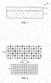
- FIG. 1 is a sectional view for schematically illustrating a semiconductor laminate film 100 according to this embodiment.
- the semiconductor laminate film 100 includes a silicon (Si) substrate 10 and a semiconductor layer 20.
- the material for the silicon substrate 10 is silicon.
- the silicon substrate 10 may be a monocrystalline substrate.
- the silicon substrate 10 may be a silicon on insulator (SOI) substrate, in which a monocrystalline silicon thin film is formed on an insulator, or a silicon on quartz (SOQ) substrate.
- SOI silicon on insulator
- SOQ silicon on quartz
- the silicon substrate 10 may be, for example, a (100) substrate.
- the silicon substrate 10 may be formed of a monocrystalline silicon substrate and a silicon layer formed on the monocrystalline silicon substrate.
- the semiconductor layer 20 is formed on the silicon substrate 10.
- the semiconductor layer 20 contains silicon (Si) and germanium (Ge).
- the semiconductor layer 20 may be a semiconductor layer containing impurities configured to impart conductivity.
- the semiconductor layer 20 is substantially lattice-matched with the silicon substrate 10 and has large compressive strain. It is preferred that the semiconductor layer 20 be lattice-matched (completely lattice-matched) with the silicon substrate 10.
- the semiconductor layer 20 may be a Si 1-x Ge x layer (where 0 ⁇ x ⁇ 1) including silicon and germanium.
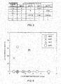
- FIG. 2 and FIG. 3 are views for illustrating a state in which a SiGe layer is lattice-matched with a Si substrate.
- a white circle represents a Si atom
- a black circle represents a Ge atom.
- the Si 1-x Ge x layer has a larger lattice constant than the Si substrate.
- Si has a lattice constant of 0.543 nm and Ge has a lattice constant of 0.565 nm, and hence the Si 1-x Ge x layer has a lattice constant of more than 0.543 nm and less than 0.565 nm.
- the semiconductor layer 20 (SiGe layer in the illustrated example) is compressed in a plane direction (in a direction perpendicular to a lamination direction) and pulled in the lamination direction, and is thus lattice-matched with the silicon substrate 10 (Si substrate in the illustrated example).
- the semiconductor layer 20 has compressive strain in the plane direction.
- the above-mentioned state in which the semiconductor layer 20 has compressive strain, and the lattice constant of the semiconductor layer 20 is matched with the lattice constant of the silicon substrate 10 is referred to as "the semiconductor layer 20 is lattice-matched with the silicon substrate 10."
- the SiGe layer when the SiGe layer is not lattice-matched with the Si substrate as illustrated in FIG. 4 , the SiGe layer includes a relaxed interfacial region 2. With this, threading dislocation caused by a mismatch defect may occur on a surface of the semiconductor laminate film. In contrast, in the semiconductor laminate film 100, the occurrence of the threading dislocation can be sufficiently reduced because the semiconductor layer 20 is substantially lattice-matched with the silicon substrate 10. Accordingly, when the semiconductor laminate film 100 is used for a semiconductor device, the occurrence of malfunction resulting from the defect is sufficiently reduced, and the reliability of the semiconductor device can be improved.
- the semiconductor layer 20 When the semiconductor layer 20 is not completely lattice-matched with the silicon substrate 10, the semiconductor layer 20 has a lattice mismatch rate f of, for example, 0.3% or less, preferably 0.1% or less. As described above, it is preferred that the semiconductor layer 20 be lattice-matched (completely lattice-matched) with the silicon substrate 10, and in this case, the semiconductor layer 20 has a lattice mismatch rate f of 0%. When the semiconductor layer 20 has a lattice mismatch rate f of 0%, the lattice spacing of the semiconductor layer 20 in the plane direction is exactly the same as the lattice spacing of the silicon substrate 10 in the plane direction, and the semiconductor layer 20 is lattice-matched with the silicon substrate 10.
- the lattice mismatch rate f (%) can be determined by the following equation (1).
- the a Si and the a SiGe may be determined by, for example, reciprocal lattice map measurement based on X-ray diffraction in a (404) crystal orientation. Even in the case where the ratio of the number of Ge atoms in the SiGe layer is increased, when the SiGe layer is substantially lattice-matched with the silicon substrate and the lattice mismatch rate f is close to 0%, a SiGe layer having large compressive strain is obtained. With this, a potential well for a hole becomes deeper, and the mobility of the hole becomes higher, and thus the characteristics of the device are significantly improved.
- f a SiGe ⁇ a Si / a Si ⁇ 100
- the semiconductor laminate film 100 satisfies the relationship represented by the following expression (2). It is preferred that the semiconductor laminate film 100 satisfy the relationship represented by the following expression (3). t ⁇ 0 ⁇ .881 ⁇ x ⁇ 4.79 t ⁇ 0.881 ⁇ x ⁇ 4.79
- the thickness t of the semiconductor layer 20 may be measured by, for example, observing a sectional transmission electron microscope (TEM) image.
- the composition ratio x of Ge may be measured by, for example, secondary ion mass spectrometry (SIMS) or X-ray diffraction (XRD) spectroscopy.
- SIMS secondary ion mass spectrometry
- XRD X-ray diffraction
- the composition ratio x of Ge is 0.30 or less.
- the composition ratio x of Ge is 0.355 or less.
- the thickness t is 50 nm or less, the composition ratio x of Ge is 0.43 or less.
- the semiconductor layer 20 has a thickness t ranging, for example, from 1 nm to 1 ⁇ m, preferably from 5 nm to 500 nm.
- the thickness t of the semiconductor layer 20 refers to a maximum value of magnitude of the semiconductor layer 20 in the lamination direction.
- the semiconductor layer 20 has a surface roughness Rms (root mean square surface roughness) of 1 nm or less, preferably 0.5 nm or less.
- SiGe has a lattice constant of 0.543 nm or more, and hence when the Rms is 0.5 nm, the semiconductor layer 20 can have a surface roughness smaller than the lattice constant of SiGe.
- the surface roughness Rms is a root mean square roughness, and may be measured with an atomic force microscope (AFM).
- the semiconductor layer 20 may contain at least one of carbon (C) or tin (Sn) as an additive.
- concentration of C and Sn to be added as an additive is 20% or less with respect to a total number of atoms in the semiconductor layer 20.
- C or Sn is added to the semiconductor layer 20
- the lattice constant of the semiconductor layer 20 can be controlled.
- C has a lattice constant of 0.356 nm, which is smaller than the lattice constant of SiGe. Therefore, when C is added, the lattice constant of the semiconductor layer 20 can be reduced.
- the semiconductor layer 20 may be a Si 1-x-y Ge x C y (0 ⁇ y ⁇ x) layer including Si, Ge, and C.
- the semiconductor layer 20 may be a Si 1-x-y Ge x Sn y (0 ⁇ y ⁇ x) layer including Si, Ge, and Sn.
- the semiconductor laminate film 100 has the following features.
- the semiconductor laminate film 100 satisfies the above-mentioned expression (2).
- the semiconductor layer 20 can have larger compressive strain (i.e., a lower lattice mismatch rate f) than a semiconductor layer formed by, for example, a CVD method (see the details described later).
- a semiconductor layer formed by, for example, a CVD method see the details described later.
- the semiconductor laminate film 100 even when the semiconductor layer 20 has a high composition ratio of Ge, the semiconductor layer 20 is better lattice-matched with the silicon substrate 10, and a semiconductor device having satisfactory characteristics can be produced.
- the semiconductor laminate film 100 is used for a semiconductor device, a deep potential well for a hole can be formed in a valence band.
- the SiGe layer is used as a channel, the mobility (speed) of a hole passing therethrough can be increased. Thus, an increase in speed of the device can be achieved.
- the semiconductor layer 20 has a surface roughness Rms of 1 nm or less. As described above, the surface roughness Rms of the semiconductor layer 20 can be reduced in the semiconductor laminate film 100, and hence when the semiconductor laminate film 100 is used for the semiconductor device, a high-density device can be produced.
- the semiconductor laminate film 100 can include the semiconductor layer 20 capable of producing the semiconductor device having satisfactory characteristics.
- the semiconductor layer 20 may have a surface roughness Rms of 0.5 nm or less. Therefore, in the semiconductor laminate film 100, the surface roughness Rms of the semiconductor layer 20 can be reduced to be smaller than the lattice constant of SiGe, and a higher-density device can be produced.
- the semiconductor laminate film 100 may satisfy the above-mentioned expression (3).
- the lattice mismatch rate f can be reduced to 0%, and the semiconductor layer 20 is lattice-matched with the silicon substrate 10.
- FIG. 5 is a flowchart for illustrating the method of producing the semiconductor laminate film 100 according to this embodiment.
- the silicon substrate 10 is prepared (Step S1).
- the semiconductor layer 20 is formed on the silicon substrate 10 by a sputtering method (Step S2).
- a sputtering gas is introduced into a chamber of a sputtering device, and a voltage is applied to a target to generate glow discharge and ionize atoms of the sputtering gas.
- the resultant gas ions are caused to collide with a surface of the target at high speed, and thus particles of a film formation material constituting the target are sputtered to deposit on a surface of the substrate, to thereby form a thin film.
- the sputtering device there is used, for example, a device in which a vacuum reaction vessel (chamber) and a sample introduction vessel (chamber) are connected to each other through a vacuum valve.
- the formation temperature of the semiconductor layer 20 is less than 600 °C, preferably 350 °C or more and 550 °C or less, more preferably 350 °C or more and 450 °C or less.
- the film formation temperature is less than 350 °C, an activation rate of a dopant may be remarkably reduced in the case where a dopant (impurities), such as phosphorus, arsenic, antimony, boron, or gallium, is injected into the semiconductor layer 20.
- a dopant such as phosphorus, arsenic, antimony, boron, or gallium
- the impurities can be activated without heating after the film formation, and the semiconductor layer 20 containing impurities configured to impart conductivity can be formed.
- the film formation temperature of the semiconductor layer 20 refers to, for example, a substrate temperature of the silicon substrate 10 at the time of formation of the semiconductor layer 20 on the silicon substrate 10.
- the semiconductor layer 20 containing impurities may be formed by, for example, using a sputtering target in which impurities are mixed.
- the semiconductor layer 20 containing impurities may be formed by performing ion implantation after the film formation by the sputtering method.
- the semiconductor layer 20 containing impurities may be formed by performing heat diffusion using a gas containing impurities after the film formation by the sputtering method.
- the semiconductor layer 20 may be formed by performing the sputtering method a plurality of times. That is, the semiconductor layer 20 may have a laminate structure of a plurality of layers. In this case, impurities may be incorporated in any one of the layers constituting the laminate structure, or may be incorporated in all the layers constituting the laminate structure.
- the silicon substrate 10 Before the formation of the semiconductor layer 20 on the silicon substrate 10, the silicon substrate 10 may be cleaned by, for example, being heated to 1,000 °C or more and 1,100 °C or less. With this, impurities contained in the silicon substrate 10 can be removed.
- the formation pressure of the semiconductor layer 20 ranges from 1 mTorr to 11 mTorr, preferably from 2 mTorr to 10 mTorr, more preferably from 2 mTorr to 5 mTorr still more preferably from 2 mTorr to 4 mTorr.
- the formation pressure of the semiconductor layer 20 is less than 1 mTorr, such instability that discharge does not start may occur.
- the formation pressure of the semiconductor layer 20 is more than 11 mTorr, the lattice mismatch rate f may be increased.
- the formation pressure of the semiconductor layer 20 refers to, for example, the pressure of a chamber (chamber of the sputtering device) in which the silicon substrate 10 is placed at the time of formation of the semiconductor layer 20 on the silicon substrate 10.
- the sputtering method for forming the semiconductor layer 20 is performed under any of first conditions and second conditions described below.
- the film formation temperature is less than 500 °C, and the film formation pressure ranges from 1 mTorr to 11 mTorr.
- the film formation temperature is less than 600 °C, and the film formation pressure is equal to or more than 2 mTorr and less than 5 mTorr.
- the sputtering gas has a volume ratio of a hydrogen gas of 0.1% or less, preferably 0.0001% or less, more preferably 0%.
- the lattice mismatch rate f may be increased, or crystallization may not occur in the first place.
- a mixed gas of an inert gas, such as argon (Ar), and a hydrogen gas, or an argon gas may be used as the sputtering gas.
- argon (Ar) argon
- argon gas a commercially available argon gas has a purity of about 99.9999%, and hydrogen is mixed therein at a ratio of 0.0001% or less. The same applies to the purities of other inert gases.
- a flow rate of the sputtering gas ranges, for example, from 0.1 cc/min to 10,000 cc/min when the sputtering gas to be supplied has a temperature of 0 °C under the atmospheric pressure.
- the flow rate of the sputtering gas is set to fall within the above-mentioned range, the semiconductor layer 20 having compressive strain can be formed more reliably.
- a high-frequency power of the sputtering device ranges, for example, from 0.1 W/cm 2 to20 W/cm 2 per unit area of the target.
- the direct-current power is, for example, 0.1 W/cm 2 or more and 10 W/cm 2 or less.
- the semiconductor laminate film 100 can be produced.
- the sputtering gas has a volume ratio of a hydrogen gas of less than 0.1%, and the sputtering method for forming the semiconductor layer 20 is performed under any of the first conditions and the second conditions described above. Further, in the method of producing the semiconductor laminate film 100, the above-mentioned expression (2) is satisfied. Therefore, in the method of producing the semiconductor laminate film 100, the semiconductor layer 20 having larger compressive strain (i.e., a lower lattice mismatch rate f) than a semiconductor layer formed under the film formation conditions of, for example, a volume ratio of a hydrogen gas of the sputtering gas of 0.1% or more can be formed (the details are described later).
- the semiconductor layer 20 can be grown so as to be lattice-matched with the silicon substrate 10.
- the semiconductor laminate film 100 capable of producing a semiconductor device having satisfactory characteristics can be produced.
- the sputtering gas may have a volume ratio of a hydrogen gas of 0.0001% or less.
- the semiconductor layer 20 having a lattice mismatch rate f of 0% can be formed (the details are described later).
- a SiGe layer was formed on a Si substrate by a sputtering method with a device in which a vacuum reaction vessel (chamber) and a sample introduction vessel (chamber) were connected to each other through a vacuum valve.
- the vacuum reaction vessel is equipped with a magnetron sputtering gun for Si and a magnetron sputtering gun for Ge.
- the vacuum reaction vessel was evacuated to vacuum. More specifically, the vacuum valve was closed, and the vacuum reaction vessel was evacuated to 1 ⁇ 10 -9 Torr or less. Moreover, while the vacuum valve was closed, the Si substrate was placed in the sample introduction vessel. Next, the sample introduction vessel was evacuated to a vacuum of 1 ⁇ 10 -7 Torr or less with a turbomolecular pump and a rotary pump each connected to the sample introduction vessel.
- the vacuum valve was opened, and the Si substrate was placed at a predetermined position of the vacuum reaction vessel.
- the vacuum valve was closed, and the vacuum reaction vessel was evacuated to a pressure of 1 ⁇ 10 -9 Torr or less in an ultra-high vacuum region.
- the Si substrate placed at the predetermined position was cleaned by being heated to 800 °C or more with a heater.
- a sputtering gas was introduced into the vacuum reaction vessel, and the flow rate of the sputtering gas was adjusted so that the sputtering gas in the vacuum reaction vessel achieved a predetermined pressure.
- the temperature of the Si substrate was adjusted to a predetermined value with the heater.
- a sputtering target was covered with a shutter, and sputtering was started by applying a high-frequency power to the sputtering gun for Si from a high-frequency power source and applying a direct-current power to a Ge target.
- Si and Ge having flown from the sputtering target adhere to a back surface of the shutter, and do not reach a surface of the Si substrate.
- the shutter was opened so that the sputtering target was viewed from the surface of the Si substrate.
- Film formation is started when Si atoms and Ge atoms having been sputtered reach the Si substrate.
- the sputtering rates of Si and Ge, and the ratio (composition ratio) x of the number of Ge atoms to the sum of the number of Si atoms and the number of Ge atoms were controlled with the high-frequency power and the direct-current power in advance.
- the SiGe layer was formed on the Si substrate.
- the supply of the power to the sputtering guns was stopped, introduction of the sputtering gas was stopped, and the heating with the heater was stopped.
- the Si substrate having formed thereon the SiGe layer was taken out to a sample introduction vessel side by a reverse procedure to the procedure of its introduction into the vacuum reaction vessel. Specifically, while the pressure of the vacuum reaction vessel was kept at 1 ⁇ 10 -7 Torr or less, the Si substrate was transferred to the sample introduction vessel, and the vacuum valve was closed. After the vacuum valve was closed, the vacuum reaction vessel was evacuated to 1 ⁇ 10 -9 Torr or less with a vacuum pump connected to the vacuum reaction vessel, and the degree of vacuum was maintained.
- a SiGe (Si 0.7 Ge 0.3 ) layer was formed on a Si substrate by the method described in the section "3.1.”
- the thickness of the SiGe layer was set to 30 nm.
- the formation pressure of the SiGe layer was set to 3 mTorr.
- the SiGe layer was formed by using, as a sputtering gas, the following three kinds of gases: an Ar gas having a purity of 99.9999% (containing 0.0001% or less of a hydrogen gas etc.); a mixed gas of 99.9% of an Ar gas and 0.1% of a hydrogen gas; and a mixed gas of 95% of an Ar gas and 5% of a hydrogen gas ("%" represents a volume ratio), and setting the film formation temperature to 370 °C, 400 °C, 450 °C, 500 °C, and 560 °C.
- an Ar gas having a purity of 99.9999% containing 0.0001% or less of a hydrogen gas etc.
- a mixed gas of 99.9% of an Ar gas and 0.1% of a hydrogen gas a mixed gas of 95% of an Ar gas and 5% of a hydrogen gas
- % represents a volume ratio
- the lattice mismatch rate f of the SiGe layer formed as described above was determined.
- the lattice constants of Si and SiGe were determined by a reciprocal lattice map based on X-ray diffraction in a (404) crystal orientation or a (224) crystal orientation, and the lattice mismatch rate f was determined by the above-mentioned equation (1).
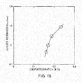
- FIG. 6 is a table for illustrating a relationship among the ratio (volume ratio) of hydrogen in the sputtering gas, the film formation temperature, and the lattice mismatch rate.
- FIG. 7 is a chart obtained by plotting the values in the table of FIG. 6 .
- FIG. 6 also the state of the SiGe layer is illustrated.
- the "crystalline” refers to a case in which a peak was observed in the X-ray diffraction
- the "amorphous” refers to a case in which a peak was not observed in the X-ray diffraction.
- FIG. 7 the boundary between the "crystalline” and the “amorphous” is represented by the broken line. The state at a temperature higher than the broken line corresponds to the "crystalline”, and the state at a temperature lower than the broken line corresponds to the "amorphous".
- the lattice mismatch rate f became lower.
- the ratio of the hydrogen gas was 5%
- the lattice mismatch rate f exceeded 0.3%
- the lattice mismatch rate f was less than 0.3%.
- the ratio of the hydrogen gas was 0.1%
- the result was obtained that, when the temperature exceeded 500 °C and approached 600 °C, the lattice mismatch rate f was drastically reduced and nearly lattice matching conditions were achieved. This is presumably because hydrogen is desorbed from the SiGe layer at high temperature, and lattice matching is easily achieved.
- the ratio of the hydrogen gas was 0.0001% or less
- the lattice mismatch rate f was 0%.
- a SiGe (Si 0.77 Ge 0.23 ) layer was formed on a Si substrate by the method described in the section "3.1.”
- the thickness of the SiGe layer was set to 273 nm.
- an Ar gas having a purity of 99.9999% (containing 99.9999% of an Ar gas and 0.0001% or less of a hydrogen gas etc.) was used.
- the film formation pressure was set to 1.2 mTorr, 2 mTorr, 3.5 mTorr, 5 mTorr, 7 mTorr, and 10 mTorr.
- the film formation temperature was set to 400 °C, 450 °C, 500 °C, and 600 °C.
- the conditions were set to the above-mentioned film formation temperature range in view of general applications of the film formation temperature because the activation rate of impurities decreased in a film formation temperature range of less than 350 °C, and the surface flatness decreased in a film formation temperature range of more than 600 °C.
- FIG. 8 is a table for illustrating a relationship among the film formation pressure, the film formation temperature, and the lattice mismatch rate f.
- FIG. 9 is a chart obtained by plotting the values in the table of FIG. 8 .
- the lattice mismatch rate f when the film formation temperature was less than 500 °C and the film formation pressure ranged from 1 mTorr to 11 mTorr, the lattice mismatch rate f was almost 0% (under the first conditions described above). In addition, when the film formation temperature was less than 600 °C and the film formation pressure ranged from 2 mTorr to 5 mTorr, the lattice mismatch rate f was almost 0% (under the second conditions described above). Further, when the film formation temperature ranged from 400 °C to 500 °C and the film formation pressure ranged from 2 mTorr to 4 mTorr, the lattice mismatch rate f was 0%.
- the film formation temperature was set to less than 500 °C
- the film formation pressure was set to range from 1 mTorr to 11 mTorr
- the volume ratio of a hydrogen gas in the sputtering gas was set to less than 0.1%
- the SiGe layer having large compressive strain as compared to a case in which the volume ratio of a hydrogen gas in the sputtering gas was set to, for example, 0.1% or more was able to be formed.
- the film formation temperature was set to less than 600 °C
- the film formation pressure was set to equal to or more than 2 mTorr and less than 5 mTorr, and the volume ratio of a hydrogen gas in the sputtering gas was set to less than 0.1%
- the SiGe layer having large compressive strain as compared to a case in which the volume ratio of a hydrogen gas in the sputtering gas was set to, for example, more than 0.1% was able to be formed.
- a Si 1-x Ge x layer was formed on a Si substrate by the method described in the section "3.1.”
- a sputtering gas an Ar gas having a purity of 99.9999% (containing 99.9999% of an Ar gas and 0.0001% or less of a hydrogen gas etc.) was used.
- the film formation temperature was set to 400 °C, and the film formation pressure was set to 3.5 mTorr.
- the thickness t of the Si 1-x Ge x layer was set to 50 nm, 125 nm, and 280 nm, the composition ratio x of Ge in the Si 1-x Ge x layer which grew so as to be lattice-matched with the Si substrate was determined.
- FIG. 10 is a table for illustrating a relationship among the composition ratio of Ge, the thickness, and the lattice mismatch rate f.
- FIG. 11 is a chart obtained by plotting the values in the table of FIG. 10 .
- FIG. 10 the results of a Si 1-x Ge x layer (74 nm) formed on a Si substrate by a CVD method were also illustrated as Comparative Example.
- FIG. 12 is a chart obtained by plotting the values in the case of a CVD method in the table of FIG. 10 .
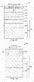
- FIG. 14 is a table for illustrating a relationship among the composition ratio of Ge, the thickness, and the surface roughness.
- FIG. 15 is a chart obtained by plotting the values in the case of a sputtering method illustrated in the table of FIG. 14 .
- FIG. 16 is a chart obtained by plotting the values in the case of a CVD method illustrated in the table of FIG. 14 .
- a semiconductor device including the semiconductor laminate film according to the invention is described.
- a semiconductor device including the above-mentioned semiconductor laminate film 100 as the semiconductor laminate film according to the invention is described below.
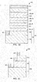
- FIG. 17 is a sectional view for schematically illustrating a first semiconductor device 210 according to an embodiment of the invention.
- the first semiconductor device 210 is a HEMT using holes as carriers (p-HEMT or a high hole mobility transistor (HHMT)).
- the first semiconductor device 210 includes: a silicon substrate 10; a semiconductor layer 20; a Si spacer layer 211; a Si supply layer 212; a Si spacer layer 213; a Si cap layer 214; a gate electrode 215; a source electrode 216; and a drain electrode 217.
- the silicon substrate 10 includes: a n-type (100) Si substrate 10a; and an i-type Si layer 10b arranged on the Si substrate 10a.
- the Si substrate 10a may be a monocrystalline substrate.
- the silicon substrate 10 may be a silicon on insulator (SOI) substrate, in which a monocrystalline silicon thin film is formed on an insulator, or a silicon on quartz (SOQ) substrate.
- SOI silicon on insulator
- SOQ silicon on quartz
- the Si layer 10b has a thickness of, for example, about 40 nm.
- the semiconductor layer 20 is arranged on the silicon substrate 10.
- the semiconductor layer 20 is of an i type.
- the semiconductor layer 20 has a thickness of, for example, about 10 nm.
- the semiconductor layer 20 is a channel layer using holes as carriers.
- the Si spacer layer 211 is arranged on the semiconductor layer 20.
- the Si spacer layer 211 is of an i type.
- the Si spacer layer 211 has a thickness of, for example, 1 nm or more and 10 nm or less.
- the Si supply layer 212 is arranged on the Si spacer layer 211.
- the Si supply layer 212 is of a p type.
- the Si supply layer 212 has a thickness of, for example, 1 nm or more and 10 nm or less.
- the Si supply layer 212 is configured to supply a carrier (hole) to the semiconductor layer 20.
- the Si spacer layer 213 is arranged on the Si supply layer 212.
- the Si spacer layer 213 is of an i type.
- the Si spacer layer 213 has a thickness of, for example, 1 nm or more and 10 nm or less.
- the gate electrode 215 is arranged on the Si spacer layer 213.
- the Si cap layer 214 is arranged on the Si spacer layer 213.
- the Si cap layer 214 is of a p type.
- the Si cap layer 214 has a thickness of, for example, 5 nm or more and 50 nm or less.
- the source electrode 216 and the drain electrode 217 are arranged on the Si cap layer 214.
- a SiO 2 layer, a SiN layer, an insulating resist layer, or the like is arranged as a protective layer 218 on the Si cap layer 214.
- the protective layer 218 may not be arranged.
- the first semiconductor device 210 includes the semiconductor layer 20.
- the semiconductor layer 20 can be reduced in lattice mismatch rate f and thus can have large compressive strain.
- the compressive strain can be increased more, and a carrier mobility can be increased more.
- an increase in carrier mobility can be achieved, and thus an increase in speed can be achieved by increasing the composition ratio x of Ge and increasing the compressive strain.
- the semiconductor layer 20 does not include a dopant atom, and a hole carrier does not suffer from impurities scattering, with the result that a reduction in carrier mobility does not occur.
- the hole carrier configured to impart electrical conductivity to the semiconductor layer 20 is supplied from the Si supply layer 212.
- FIG. 18 is a sectional view for schematically illustrating a second semiconductor device 220 according to an embodiment of the invention.
- the second semiconductor device 220 is a doped channel field effect transistor (DCFET) using holes as carriers (p-DCFET).
- DCFET doped channel field effect transistor
- p-DCFET holes as carriers
- the second semiconductor device 220 includes: a silicon substrate 10; a semiconductor layer 20; a Si cap layer 221; a gate electrode 222; a source electrode 223; and a drain electrode 224.
- the silicon substrate 10 includes: a n-type (100) Si substrate 10a; and an i-type Si layer 10b arranged on the Si substrate 10a.
- the Si substrate 10a may be a monocrystalline substrate.
- the silicon substrate 10 may be a silicon on insulator (SOI) substrate, in which a monocrystalline silicon thin film is formed on an insulator, or a silicon on quartz (SOQ) substrate.
- SOI silicon on insulator
- SOQ silicon on quartz
- the Si layer 10b has a thickness of, for example, 10 nm or more and 100 nm or less.
- the semiconductor layer 20 is arranged on the silicon substrate 10.
- the semiconductor layer 20 is of a p type.
- the semiconductor layer 20 has a thickness of, for example, 10 nm or more and 100 nm or less.
- the semiconductor layer 20 is a channel layer using holes as carriers.
- the source electrode 223 and the drain electrode 224 are arranged on the semiconductor layer 20.
- the Si cap layer 221 is arranged on the semiconductor layer 20.
- the Si cap layer 221 is of an i type.
- the Si cap layer 221 has a thickness of, for example, 10 nm or more and 100 nm or less.
- the gate electrode 222 is arranged on the Si cap layer 214.
- the second semiconductor device 220 includes the semiconductor layer 20.
- the semiconductor layer 20 can be reduced in lattice mismatch rate f and thus can have large compressive strain.
- the composition ratio x of Ge is increased more, the compressive strain is increased more, and a hole mobility is increased more. Accordingly, in the second semiconductor device 220, a further increase in speed can be achieved by increasing the composition ratio x of Ge and increasing the compressive strain.
- FIG. 19 is a sectional view for schematically illustrating a third semiconductor device 230 according to an embodiment of the invention.
- the third semiconductor device 230 is a hole tunneling resonant tunneling diode (RTD) (p-RTD).
- the third semiconductor device 230 includes: a silicon substrate 10; a semiconductor layer 20; a Si layer 231; a Si layer 232; an electrode layer 233 formed of, for example, Al; and an electrode layer 234 formed of, for example, Al.
- the third semiconductor device 230 includes four SiGe semiconductor layers 20a, 20b, 20c, and 20d.
- the silicon substrate 10 includes: a p-type (100) Si substrate 10a; and a p-type Si layer 10b arranged on the Si substrate 10a.
- the Si substrate 10a may be a monocrystalline substrate.
- the silicon substrate 10 may be a silicon on insulator (SOI) substrate, in which a monocrystalline silicon thin film is formed on an insulator, or a silicon on quartz (SOQ) substrate.
- SOI silicon on insulator
- SOQ silicon on quartz
- the Si layer 10b has a thickness of, for example, 10 nm or more and 100 nm or less.
- the electrode layer 233 is arranged on the Si substrate 10a.
- the electrode layer 233 is one of electrodes of the third semiconductor device 230.
- the semiconductor layer 20a is arranged on the silicon substrate 10.
- the SiGe semiconductor layers 20a, 20b, 20c, and 20d are laminated in the stated order, and the Si layers 231 are arranged between the semiconductor layers 20a, 20b, 20c, and 20d.
- the semiconductor layers 20a, 20b, 20c, and 20d are each formed of i-type SiGe.
- the semiconductor layers 20a and 20d each have a thickness of, for example, 10 nm or more and 100 nm or less.
- the semiconductor layers 20b and 20c each have a thickness of, for example, 1 nm or more and 6 nm or less.
- the Si layers 231 are each of an i type.
- the Si layers 231 each have a thickness of, for example, 1 nm or more and 3 nm or less.
- the semiconductor layers 20b and 20c are each a quantum well layer, and the Si layers 231 are each a barrier layer.
- the Si layer 232 is arranged on the semiconductor layer 20d.
- the Si layer 232 is of a p type.
- the Si layer 232 has a thickness of, for example, 10 nm or more and 100 nm or less.
- the electrode layer 234 formed of, for example, Al is arranged on the Si layer 232.
- the electrode layer 234 is the other one of the electrodes of the third semiconductor device 230.
- the third semiconductor device 230 includes the semiconductor layer 20.
- the semiconductor layer 20 can have large compressive strain.
- the hole tunneling RTD as the composition ratio x of Ge is increased more and the compressive strain is increased more, a deep potential well is formed more easily, and a larger resonant current is obtained, with the result that an operation speed is increased more. Accordingly, in the third semiconductor device 230, a further increase in speed can be achieved by increasing the composition ratio x of Ge and increasing the compressive strain.
- FIG. 20 is a sectional view for schematically illustrating a fourth semiconductor device 240 according to an embodiment of the invention.
- the fourth semiconductor device 240 is a npn-type hetero-bipolar transistor (HBT).
- the fourth semiconductor device 240 includes: a silicon substrate 10; a semiconductor layer 20; a Si layer 241; a collector electrode 242; a base electrode 243; and an emitter electrode 244.
- the silicon substrate 10 is a n-type (100) Si substrate.
- the silicon substrate 10 corresponds to a collector region.
- a n-type Si layer may be arranged on the silicon substrate 10.
- the collector electrode 242 is arranged on the silicon substrate 10.
- the silicon substrate 10 may be a monocrystalline substrate.
- the silicon substrate 10 may be a silicon on insulator (SOI) substrate, in which a n-type monocrystalline silicon thin film is formed on an insulator, or a silicon on quartz (SOQ) substrate.
- SOI silicon on insulator
- SOQ silicon on quartz
- the silicon substrate 10 may be a SOI substrate or a SOQ substrate having formed thereon a n-type Si layer.
- the semiconductor layer 20 is arranged on the silicon substrate 10.
- the semiconductor layer 20 corresponds to a base region.
- the composition ratio x of Ge in the semiconductor layer 20 may vary in a direction perpendicular to a surface of the substrate.
- the semiconductor layer 20 is of a p type.
- the semiconductor layer 20 has a thickness of, for example, 30 nm or more and 200 nm or less.
- the base electrode 243 is arranged on the semiconductor layer 20.
- the Si layer 241 is arranged on the semiconductor layer 20.
- the Si layer 241 is of a n type.
- the Si layer 241 corresponds to an emitter region.
- the Si layer 241 has a thickness of, for example, 20 nm or more and 100 nm or less.
- the emitter electrode 244 is arranged on the Si layer 241.
- the fourth semiconductor device 240 includes the semiconductor layer 20. As described above, even when the semiconductor layer 20 has a large composition ratio x of Ge, the semiconductor layer 20 can be lattice-matched or substantially lattice-matched with the silicon substrate 10 or the n-type silicon layer arranged on the silicon substrate. In the npn-type HBT, as the composition ratio x of Ge is increased more, a larger potential barrier is formed for a hole in a valence band at a boundary between the emitter region and the base region, and a current amplification factor can be increased more. Accordingly, in the fourth semiconductor device 240, an increase in current amplification factor can be achieved, and a further increase in speed can be achieved by increasing the composition ratio x of Ge and increasing the compressive strain.
- the semiconductor laminate film 100 may be used for a MOSFET with a strained SiGe channel using holes as carriers (strained-SiGe-channel p-MOSFET), or a MOSFET with a buried-SiGe-channel using holes as carriers (buried-channel p-MOSFET).
- the buried-channel p-MOSFET can be realized by replacing the Si cap layer 221 of the second semiconductor device 220 with the following two layers laminated on each other: an i-type Si spacer layer; and an insulating layer, such as a SiO 2 layer.
- the i-type Si spacer layer is arranged on the lower side of the two layers.
- the semiconductor laminate film including the SiGe layer which has a low lattice mismatch rate, and is substantially lattice-matched or lattice-matched with the Si substrate, and which has a large composition ratio of Ge can be produced.
- Utilization of a semiconductor device using the technology for the semiconductor laminate film according to the invention is expected to contribute to an increase in performance and a reduction in cost of an electronic device component for millimeter waveband applications.
- the semiconductor device is expected to significantly contribute to advancement of, for example, wireless communication or a radar in a millimeter waveband, object image detection, and a non-invasive and non-destructive test as an electronic device technology serving as a foundation for high-frequency electronics and measurement sensing technologies in the future in industrial technical fields related to sensor networks, artificial intelligence (AI), internet of things (IoT), and the like.
- the semiconductor laminate film according to the invention is particularly effective for an increase in performance of a p-type channel transistor, which is inferior in performance of an operation speed to a n-type channel transistor, and also enables a remarkable reduction in power consumption by achieving a high-frequency amplifier with a complementary configuration.
- the invention includes configurations that are substantially the same (for example, in function, method, and results, or in objective and effects) as the configurations described in the embodiments.
- the invention also includes configurations in which non-essential elements described in the embodiments are replaced by other elements.
- the invention also includes configurations having the same effects as those of the configurations described in the embodiments, or configurations capable of achieving the same objectives as those of the configurations described in the embodiments.
- the invention further includes configurations obtained by adding known art to the configurations described in the embodiments.
Landscapes
- Chemical & Material Sciences (AREA)
- Organic Chemistry (AREA)
- Engineering & Computer Science (AREA)
- Materials Engineering (AREA)
- Mechanical Engineering (AREA)
- Metallurgy (AREA)
- Chemical Kinetics & Catalysis (AREA)
- Physical Deposition Of Substances That Are Components Of Semiconductor Devices (AREA)
- Physical Vapour Deposition (AREA)
- Recrystallisation Techniques (AREA)
- Bipolar Transistors (AREA)
- Junction Field-Effect Transistors (AREA)
- Thin Film Transistor (AREA)
Applications Claiming Priority (2)
| Application Number | Priority Date | Filing Date | Title |
|---|---|---|---|
| JP2016140117 | 2016-07-15 | ||
| PCT/JP2017/025436 WO2018012546A1 (ja) | 2016-07-15 | 2017-07-12 | 半導体積層膜の製造方法、および半導体積層膜 |
Publications (2)
| Publication Number | Publication Date |
|---|---|
| EP3486940A1 true EP3486940A1 (de) | 2019-05-22 |
| EP3486940A4 EP3486940A4 (de) | 2020-02-19 |
Family
ID=60953052
Family Applications (1)
| Application Number | Title | Priority Date | Filing Date |
|---|---|---|---|
| EP17827672.1A Pending EP3486940A4 (de) | 2016-07-15 | 2017-07-12 | Herstellungsverfahren für halbleiterlaminierte folie sowie halbleiterlaminierte folie |
Country Status (5)
| Country | Link |
|---|---|
| US (2) | US11492696B2 (de) |
| EP (1) | EP3486940A4 (de) |
| JP (1) | JP6890802B2 (de) |
| TW (1) | TWI728151B (de) |
| WO (1) | WO2018012546A1 (de) |
Families Citing this family (1)
| Publication number | Priority date | Publication date | Assignee | Title |
|---|---|---|---|---|
| CN109972099B (zh) * | 2019-05-10 | 2020-11-27 | 福建农林大学 | 一种制备片状氧化铁的方法 |
Family Cites Families (12)
| Publication number | Priority date | Publication date | Assignee | Title |
|---|---|---|---|---|
| US3993533A (en) * | 1975-04-09 | 1976-11-23 | Carnegie-Mellon University | Method for making semiconductors for solar cells |
| US6855649B2 (en) | 2001-06-12 | 2005-02-15 | International Business Machines Corporation | Relaxed SiGe layers on Si or silicon-on-insulator substrates by ion implantation and thermal annealing |
| JP3970011B2 (ja) * | 2001-12-11 | 2007-09-05 | シャープ株式会社 | 半導体装置及びその製造方法 |
| US7187059B2 (en) * | 2004-06-24 | 2007-03-06 | International Business Machines Corporation | Compressive SiGe <110> growth and structure of MOSFET devices |
| JP2010226136A (ja) | 2004-08-31 | 2010-10-07 | Tokyo Univ Of Agriculture & Technology | 半導体薄膜製造方法 |
| JP4910124B2 (ja) | 2004-08-31 | 2012-04-04 | 国立大学法人東京農工大学 | 半導体薄膜製造装置および方法 |
| US7514726B2 (en) * | 2006-03-21 | 2009-04-07 | The United States Of America As Represented By The Aministrator Of The National Aeronautics And Space Administration | Graded index silicon geranium on lattice matched silicon geranium semiconductor alloy |
| JP2008021674A (ja) | 2006-07-10 | 2008-01-31 | Tokyo Univ Of Agriculture & Technology | 半導体積層膜、及び半導体積層膜作製用装置 |
| JP2008198656A (ja) * | 2007-02-08 | 2008-08-28 | Shin Etsu Chem Co Ltd | 半導体基板の製造方法 |
| JP5216716B2 (ja) * | 2008-08-20 | 2013-06-19 | 株式会社半導体エネルギー研究所 | 発光装置及びその作製方法 |
| CN101866834B (zh) * | 2009-12-11 | 2011-09-14 | 清华大学 | 高Ge组分SiGe材料的方法 |
| JP2015153775A (ja) * | 2014-02-10 | 2015-08-24 | 国立大学法人東京農工大学 | 高移動度トランジスタおよびその製造方法 |
-
2017
- 2017-07-12 JP JP2018527637A patent/JP6890802B2/ja active Active
- 2017-07-12 EP EP17827672.1A patent/EP3486940A4/de active Pending
- 2017-07-12 WO PCT/JP2017/025436 patent/WO2018012546A1/ja not_active Ceased
- 2017-07-12 US US16/317,751 patent/US11492696B2/en active Active
- 2017-07-14 TW TW106123693A patent/TWI728151B/zh active
-
2021
- 2021-03-10 US US17/197,137 patent/US11972947B2/en active Active
Also Published As
| Publication number | Publication date |
|---|---|
| US20210189549A1 (en) | 2021-06-24 |
| US20190242008A1 (en) | 2019-08-08 |
| TWI728151B (zh) | 2021-05-21 |
| US11972947B2 (en) | 2024-04-30 |
| JP6890802B2 (ja) | 2021-06-18 |
| WO2018012546A1 (ja) | 2018-01-18 |
| JPWO2018012546A1 (ja) | 2019-05-23 |
| EP3486940A4 (de) | 2020-02-19 |
| TW201812857A (zh) | 2018-04-01 |
| US11492696B2 (en) | 2022-11-08 |
Similar Documents
| Publication | Publication Date | Title |
|---|---|---|
| Leitz et al. | Hole mobility enhancements and alloy scattering-limited mobility in tensile strained Si/SiGe surface channel metal–oxide–semiconductor field-effect transistors | |
| US6896731B1 (en) | P-type single crystal zinc-oxide having low resistivity and method for preparation thereof | |
| CN103781947A (zh) | 外延生长用基板和晶体层叠结构体 | |
| TW201428123A (zh) | 藉由利用氮氣之鋅靶材的反應性濺鍍所產生的薄膜半導體材料 | |
| US6537369B1 (en) | SiGeC semiconductor crystal and production method thereof | |
| Dheenan et al. | β-Ga2O3 MESFETs with insulating Mg-doped buffer grown by plasma-assisted molecular beam epitaxy | |
| US10388751B2 (en) | Semiconductor device and method for forming n-type conductive channel in diamond using heterojunction | |
| Hartmann et al. | A benchmark of germane and digermane for the low temperature growth of intrinsic and heavily in-situ boron-doped SiGe | |
| US11972947B2 (en) | Manufacturing method for semiconductor laminated film, and semiconductor laminated film | |
| CN117199136A (zh) | 一种集成异质结二极管的SiC MOSFET及制备方法 | |
| EP0702413A2 (de) | Auf einer Diamantschicht gebildeter MES-Feldeffekttransistor | |
| US10804104B2 (en) | Semiconductor device and method for forming p-type conductive channel in diamond using abrupt heterojunction | |
| US20030151051A1 (en) | High performance active and passive structures based on silicon material grown epitaxially or bonded to silicon carbide substrate | |
| JP2004343133A (ja) | 炭化珪素製造方法、炭化珪素及び半導体装置 | |
| Kurishima et al. | Effect of carbon doping on threshold voltage and mobility of In-Si-O thin-film transistors | |
| Kanyandekwe et al. | Selective epitaxy of tensile, highly doped SiP for planar NMOS FD-SOI devices | |
| Kopnov et al. | High mobility conducting channel at semi-insulating GaAs–metal oxide interfaces | |
| US20250163606A1 (en) | Production method for single crystal semiconductor film, production method for multilayer film of single crystal semiconductor film, and semiconductor element | |
| CN117457749B (zh) | 一种栅极下方具有P型空间层的SiC LMOS及制备方法 | |
| SHIRAI et al. | Development of Sputtering Module" SEGul" for Forming GaN Epitaxial Thin Films | |
| JP4241174B2 (ja) | 低抵抗n型半導体ダイヤモンド | |
| Alema et al. | Nitrogen doping of metal-organic chemical vapor deposition β-Ga2O3 using nitric oxide | |
| Suda et al. | Reduced activation temperature of B impurities in Si (001) epitaxial layers grown by sputter epitaxy using B-doped Si (001) target compared with Si (111) target | |
| Lee et al. | Growth of nitrogen doped ZnO films through a nitrogen diffusion process from WN films formed by a cosputtering technique | |
| Su et al. | Strained germanium-tin pmosfet fabricated on a silicon-on-insulator substrate with relaxed ge buffer |
Legal Events
| Date | Code | Title | Description |
|---|---|---|---|
| STAA | Information on the status of an ep patent application or granted ep patent |
Free format text: STATUS: THE INTERNATIONAL PUBLICATION HAS BEEN MADE |
|
| PUAI | Public reference made under article 153(3) epc to a published international application that has entered the european phase |
Free format text: ORIGINAL CODE: 0009012 |
|
| STAA | Information on the status of an ep patent application or granted ep patent |
Free format text: STATUS: REQUEST FOR EXAMINATION WAS MADE |
|
| 17P | Request for examination filed |
Effective date: 20190215 |
|
| AK | Designated contracting states |
Kind code of ref document: A1 Designated state(s): AL AT BE BG CH CY CZ DE DK EE ES FI FR GB GR HR HU IE IS IT LI LT LU LV MC MK MT NL NO PL PT RO RS SE SI SK SM TR |
|
| AX | Request for extension of the european patent |
Extension state: BA ME |
|
| DAV | Request for validation of the european patent (deleted) | ||
| DAX | Request for extension of the european patent (deleted) | ||
| A4 | Supplementary search report drawn up and despatched |
Effective date: 20200122 |
|
| RIC1 | Information provided on ipc code assigned before grant |
Ipc: H01L 21/336 20060101ALI20200116BHEP Ipc: H01L 29/778 20060101ALI20200116BHEP Ipc: H01L 21/331 20060101ALI20200116BHEP Ipc: H01L 21/02 20060101ALI20200116BHEP Ipc: H01L 29/161 20060101ALI20200116BHEP Ipc: H01L 21/329 20060101ALI20200116BHEP Ipc: H01L 29/812 20060101ALI20200116BHEP Ipc: H01L 29/737 20060101ALI20200116BHEP Ipc: H01L 29/78 20060101ALI20200116BHEP Ipc: H01L 29/88 20060101ALI20200116BHEP Ipc: H01L 21/338 20060101ALI20200116BHEP Ipc: H01L 21/203 20060101AFI20200116BHEP Ipc: C23C 14/34 20060101ALI20200116BHEP Ipc: C23C 14/06 20060101ALI20200116BHEP |
|
| STAA | Information on the status of an ep patent application or granted ep patent |
Free format text: STATUS: EXAMINATION IS IN PROGRESS |
|
| 17Q | First examination report despatched |
Effective date: 20220120 |