EP3485303B1 - Optical stack - Google Patents
Optical stack Download PDFInfo
- Publication number
- EP3485303B1 EP3485303B1 EP17828181.2A EP17828181A EP3485303B1 EP 3485303 B1 EP3485303 B1 EP 3485303B1 EP 17828181 A EP17828181 A EP 17828181A EP 3485303 B1 EP3485303 B1 EP 3485303B1
- Authority
- EP
- European Patent Office
- Prior art keywords
- band
- optical
- blocking
- reflection
- birefringent
- Prior art date
- Legal status (The legal status is an assumption and is not a legal conclusion. Google has not performed a legal analysis and makes no representation as to the accuracy of the status listed.)
- Active
Links
Images


Classifications
-
- G—PHYSICS
- G02—OPTICS
- G02B—OPTICAL ELEMENTS, SYSTEMS OR APPARATUS
- G02B5/00—Optical elements other than lenses
- G02B5/20—Filters
- G02B5/26—Reflecting filters
-
- G—PHYSICS
- G02—OPTICS
- G02B—OPTICAL ELEMENTS, SYSTEMS OR APPARATUS
- G02B5/00—Optical elements other than lenses
- G02B5/20—Filters
- G02B5/28—Interference filters
- G02B5/285—Interference filters comprising deposited thin solid films
- G02B5/287—Interference filters comprising deposited thin solid films comprising at least one layer of organic material
-
- G—PHYSICS
- G02—OPTICS
- G02B—OPTICAL ELEMENTS, SYSTEMS OR APPARATUS
- G02B5/00—Optical elements other than lenses
- G02B5/08—Mirrors
- G02B5/0816—Multilayer mirrors, i.e. having two or more reflecting layers
- G02B5/0825—Multilayer mirrors, i.e. having two or more reflecting layers the reflecting layers comprising dielectric materials only
- G02B5/0841—Multilayer mirrors, i.e. having two or more reflecting layers the reflecting layers comprising dielectric materials only comprising organic materials, e.g. polymers
-
- G—PHYSICS
- G02—OPTICS
- G02B—OPTICAL ELEMENTS, SYSTEMS OR APPARATUS
- G02B5/00—Optical elements other than lenses
- G02B5/20—Filters
- G02B5/22—Absorbing filters
-
- G—PHYSICS
- G02—OPTICS
- G02B—OPTICAL ELEMENTS, SYSTEMS OR APPARATUS
- G02B5/00—Optical elements other than lenses
- G02B5/20—Filters
- G02B5/28—Interference filters
- G02B5/285—Interference filters comprising deposited thin solid films
-
- G—PHYSICS
- G02—OPTICS
- G02B—OPTICAL ELEMENTS, SYSTEMS OR APPARATUS
- G02B5/00—Optical elements other than lenses
- G02B5/30—Polarising elements
- G02B5/3025—Polarisers, i.e. arrangements capable of producing a definite output polarisation state from an unpolarised input state
- G02B5/3033—Polarisers, i.e. arrangements capable of producing a definite output polarisation state from an unpolarised input state in the form of a thin sheet or foil, e.g. Polaroid
- G02B5/3041—Polarisers, i.e. arrangements capable of producing a definite output polarisation state from an unpolarised input state in the form of a thin sheet or foil, e.g. Polaroid comprising multiple thin layers, e.g. multilayer stacks
- G02B5/305—Polarisers, i.e. arrangements capable of producing a definite output polarisation state from an unpolarised input state in the form of a thin sheet or foil, e.g. Polaroid comprising multiple thin layers, e.g. multilayer stacks including organic materials, e.g. polymeric layers
-
- B—PERFORMING OPERATIONS; TRANSPORTING
- B32—LAYERED PRODUCTS
- B32B—LAYERED PRODUCTS, i.e. PRODUCTS BUILT-UP OF STRATA OF FLAT OR NON-FLAT, e.g. CELLULAR OR HONEYCOMB, FORM
- B32B2255/00—Coating on the layer surface
- B32B2255/26—Polymeric coating
-
- B—PERFORMING OPERATIONS; TRANSPORTING
- B32—LAYERED PRODUCTS
- B32B—LAYERED PRODUCTS, i.e. PRODUCTS BUILT-UP OF STRATA OF FLAT OR NON-FLAT, e.g. CELLULAR OR HONEYCOMB, FORM
- B32B2307/00—Properties of the layers or laminate
- B32B2307/40—Properties of the layers or laminate having particular optical properties
- B32B2307/412—Transparent
-
- B—PERFORMING OPERATIONS; TRANSPORTING
- B32—LAYERED PRODUCTS
- B32B—LAYERED PRODUCTS, i.e. PRODUCTS BUILT-UP OF STRATA OF FLAT OR NON-FLAT, e.g. CELLULAR OR HONEYCOMB, FORM
- B32B2551/00—Optical elements
-
- B—PERFORMING OPERATIONS; TRANSPORTING
- B32—LAYERED PRODUCTS
- B32B—LAYERED PRODUCTS, i.e. PRODUCTS BUILT-UP OF STRATA OF FLAT OR NON-FLAT, e.g. CELLULAR OR HONEYCOMB, FORM
- B32B27/00—Layered products comprising a layer of synthetic resin
- B32B27/36—Layered products comprising a layer of synthetic resin comprising polyesters
-
- B—PERFORMING OPERATIONS; TRANSPORTING
- B32—LAYERED PRODUCTS
- B32B—LAYERED PRODUCTS, i.e. PRODUCTS BUILT-UP OF STRATA OF FLAT OR NON-FLAT, e.g. CELLULAR OR HONEYCOMB, FORM
- B32B7/00—Layered products characterised by the relation between layers; Layered products characterised by the relative orientation of features between layers, or by the relative values of a measurable parameter between layers, i.e. products comprising layers having different physical, chemical or physicochemical properties; Layered products characterised by the interconnection of layers
- B32B7/04—Interconnection of layers
- B32B7/12—Interconnection of layers using interposed adhesives or interposed materials with bonding properties
-
- G—PHYSICS
- G02—OPTICS
- G02B—OPTICAL ELEMENTS, SYSTEMS OR APPARATUS
- G02B26/00—Optical devices or arrangements for the control of light using movable or deformable optical elements
- G02B26/06—Optical devices or arrangements for the control of light using movable or deformable optical elements for controlling the phase of light
-
- G—PHYSICS
- G02—OPTICS
- G02B—OPTICAL ELEMENTS, SYSTEMS OR APPARATUS
- G02B5/00—Optical elements other than lenses
- G02B5/08—Mirrors
- G02B5/0816—Multilayer mirrors, i.e. having two or more reflecting layers
-
- G—PHYSICS
- G02—OPTICS
- G02B—OPTICAL ELEMENTS, SYSTEMS OR APPARATUS
- G02B5/00—Optical elements other than lenses
- G02B5/08—Mirrors
- G02B5/0816—Multilayer mirrors, i.e. having two or more reflecting layers
- G02B5/0825—Multilayer mirrors, i.e. having two or more reflecting layers the reflecting layers comprising dielectric materials only
Definitions
- Optical filters can be utilized to selectively transmit light of different wavelengths or different polarizations. Optical filters are useful in a variety of optical systems such as detector systems.
- US 6 549 254 B1 describes an optical Bragg reflection filter based on liquid crystals comprising multiple layers having a birefringence gradient to suppress side-lobes of the reflection spectrum.
- WO 99/36808 A1 describes an optical filter having multiple repetitive layer components for reflection of light in the infrared region while transmitting light in the visible region of the solar spectrum. At least one component absorbs or reflects within the reflection region of the optical filter.
- WO 2016/061 192 A1 describes an optical film comprising a stack of microlayers having overlapping harmonic reflection bands.
- an optical stack including an oriented polymeric multilayer optical film and a first non-birefringent optical filter disposed adjacent the multilayer optical film.
- the oriented polymeric multilayer optical film has a first reflection band with a first band edge having a variation across a length or a width of the multilayer optical film.
- the first band edge at normal incidence, has a design wavelength ⁇ and a characteristic deviation about the design wavelength ⁇ .
- the first non-birefringent optical filter has a first blocking band which, at normal incidence, comprises wavelengths between ⁇ - ⁇ /2 and ⁇ + ⁇ /2, such that the optical stack has a band edge variation reduced by at least 60 percent compared the variation in the first band edge.
- the first reflection band includes a wavelength range having a width of at least ⁇ that is outside of the first blocking band.
- an optical system including an oriented polymeric multilayer optical film having a first reflection band with a first band edge, and a sensor in optical communication with the oriented polymeric multilayer optical film is provided.
- Oriented polymeric multilayer optical films are useful in a wide variety of applications such as reflective polarizers or mirrors in backlight systems and optical filters in detector systems. Such films can be designed to have reflection bands in a wide variety of wavelength ranges depending on the intended application.
- Oriented polymeric multilayer optical films having a reflection band often exhibit variation in one or both band edges of the reflection band. This variation can be objectionable is some applications. According to the present description, it has been found that utilizing an optical stack that includes both an oriented (and thus birefringent) polymeric multilayer optical film and a non-birefringent optical filter can provide a substantially reduced (e.g., by at least 60 percent, or by at least 70 percent, or by at least 80 percent) band edge variation compared to the oriented polymeric multilayer optical film alone while providing a wide blocking band (e.g., a reflection band) that would not be easily obtained with a non-birefringent optical filter alone.
- a substantially reduced e.g., by at least 60 percent, or by at least 70 percent, or by at least 80 percent
- the combination of the oriented polymeric multilayer optical film and the non-birefringent optical filter results in an overall blocking band for the optical stack.
- the oriented polymeric multilayer optical film is typically a reflector for one or both of two orthogonal polarization states.
- the non-birefringent optical filter has a blocking band that can be a reflection band (e.g., utilizing alternating non-birefringent layers having different refractive indices) or an absorbing band (e.g., utilizing dyes or pigments which absorb in a desired wavelength range).
- the non-birefringent optical filter is reflective and the overall blocking band is a reflection band, and in some embodiments the non-birefringent optical filter is absorptive and the overall blocking band is absorptive in some wavelengths and reflective at other wavelengths.
- the optical stacks of the present description have an overall blocking band which has a designed shift with incidence angle.
- Such optical stacks can create an angle selective element for certain wavelengths that can be used to provide an angle limited reception zone for a sensor, to provide a limited angle of emission for a light source, or to provide a limited angle of view for a marker, for example.
- the optical stacks of the present description further provide a way to produce a customized blocking band without incurring the expense of producing a custom designed oriented polymeric multilayer optical film.
- the non-birefringent filter (or filters) can be selected to have a blocking band which overlaps a band edge (or both band edges) of a reflection band of an oriented polymeric multilayer optical film and which extends in to a desired band edge to provide a customized blocking band.
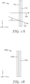
- FIG. 1A is a schematic cross-sectional view of optical stack 100 including first and second layers 110 and 114.
- One of the first and second layers 110 and 114 is an oriented polymeric multilayer optical film and the other of the first and second layers 110 and 114 is a non-birefringent optical filter.
- Light 140 is incident on the first layer 110 and the second layer 114 at normal incidence, while light 142 is incident on the first layer 110 at an oblique incidence angle of ⁇ (angle between light ray and normal vector to the first layer 110).
- the light 140 or 142 may be transmitted first through the oriented polymeric multilayer optical film and then through the non-birefringent optical filter, or the light 140 or 142 may be transmitted first through the non-birefringent optical filter and then through the oriented polymeric multilayer optical film.
- the first and second layers 110 and 114 may be disposed immediately adjacent each other as illustrated in FIG. 1A , or an air gap or an intermediate layer may be disposed between the first and second layers as illustrated in FIGS. 1B and 1C , respectively.
- the wavelength of a band edge of a reflection band or of a blocking band of interference filters typically depends on incidence angle ⁇ and typically shifts to lower wavelengths with increasing incidence angles.
- Incidence angle or angle of incidence refers to the angle between an incident light ray and a normal to the surface on which the light ray is incident (e.g., oblique incidence angle ⁇ of light 142).
- Normal incidence refers to a zero incidence angle.
- Properties of reflection bands or blocking bands, such as band edge wavelengths may be specified at normal incidence or at an oblique incidence angle.
- the oblique incidence angle used in comparing shifts of reflection or blocking bands from the corresponding bands at normal incidence can be selected to be 45 degrees or 60 degrees, for example.
- the oriented polymeric multilayer optical film may be a mirror film or a reflective polarizer film, for example.
- the oriented polymeric multilayer optical film has a first reflection band having a first band edge (e.g., left band edge) and may also have a second band edge (e.g., right band edge).
- the oriented polymeric multilayer optical film may also have a second reflection band (e.g., a higher order harmonic of the first reflection band).
- the oriented polymeric multilayer optical film is a comb filter having a plurality of reflection bands with pass bands between the reflection bands.
- the oriented polymeric multilayer optical film and the non-birefringent optical filter can be made using any of the techniques described elsewhere herein.
- the non-birefringent optical filter can be any filter in which the optically active layer(s) have isotropic refractive indices.
- Examples include interference filters having a plurality of alternating layers of differing isotropic refractive indices, as described further elsewhere herein, and include filters having an absorbing layer (e.g., dye or pigment layer) with isotropic complex refractive indices.
- Isotropic dyes or pigments may be considered a non-birefringent optical filter even if the dyes or pigments are disposed on or in an oriented substrate.
- Non-isotropic dyes or pigments such as the iodine layer in an iodine stained polyvinyl alcohol absorbing polarizer, are not non-birefringent optical filters, as used herein, since the iodine molecules are oriented and provide a birefringent complex refractive index that is different in the x- and y-directions (referring to the x-y-z coordinate system of FIG. 1A ).
- the wavelength ranges of the reflection and blocking bands can be selected based in the intended application.
- one or all of the band edges are located, at normal incidence, in a range of 300 nm, or 400 nm to 2500 nm, or 2000 nm, or 1200 nm, or 900 nm, or 700 nm.
- FIG. 1B is a schematic cross-sectional view of optical stack 100b including first and second layers 110b and 114b with an air gap therebetween.
- One of the first and second layers 110b and 114b is an oriented polymeric multilayer optical film and the other of the first and second layers 110b and 114b is a first non-birefringent optical filter.
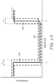
- FIG. 1C is a schematic cross-sectional view of optical stack 100c including first, second and third layers 110c, 114c and 116c.
- One of the first, second and third layers 110c, 114c and 116c is an oriented polymeric multilayer optical film and a different one of the first, second and third layers 110c, 114c and 116c is a first non-birefringent optical filter.
- the remaining layer may be an adhesive layer, for example, and/or may be a second non-birefringent optical filter (e.g., a dyed adhesive layer).
- first layer 110c is an oriented polymeric multilayer optical film
- second layer 114c is a first non-birefringent optical filter
- third layer 116c is an intermediate layer.
- the intermediate layer is an adhesive layer
- the intermediate layer includes one or more dyes or pigments which may include one or more polarizing dyes or pigments.
- the intermediate layer is an oriented polymeric layer such as oriented polyethylene terephthalate (PET).
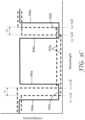
- FIG. 1D is a schematic cross-sectional view of optical stack 100d including first and second layers 110d and 114d.
- One of the first and second layers 110d and 114d is an oriented polymeric multilayer optical film and the other of the first and second layers 110d and 114d is a first non-birefringent optical filter.
- Optical stack 100d is curved about one axis (the x-axis) or about two orthogonal axes (the x-axis and the y-axis).
- Optical stack 100d can be formed using a thermoforming process or an in-mold forming process.
- first and second layers 110d and 114d are formed as separate layers which are subsequent formed (e.g., thermoformed) into the curved shape illustrated in FIG. 1D .
- an in-mold process is used where the oriented polymeric multilayer optical film is prepared and placed into a mold and a material with a wavelength selective dye or pigment is injected into the mold to form the non-birefringent optical filter. Additional layers may be formed between the oriented polymeric multilayer optical film and the non-birefringent optical filter.
- the in-mold forming results in an oriented polymeric multilayer optical film curved about at least one axis (e.g., curved about two orthogonal axes). In other embodiments, the in-mold forming results in a flat oriented polymeric multilayer optical film.
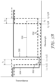
- FIG. 2 is a schematic cross-sectional view of optical stack 200 including first and second layers 210 and 214.
- One of the first and second layers 210 and 214 is an oriented polymeric multilayer optical film and the other of the first and second layers 210 and 214 is a non-birefringent optical filter.
- the first layer 210 is spatially variant and includes holes or discontinuities 218.
- first layer 210 is an oriented polymeric multilayer optical film and holes or discontinuities 218 are holes through the oriented polymeric multilayer optical film that can be formed by die cutting, for example.
- first layer 210 is a non-birefringent optical filter and holes or discontinuities 218 are discontinuities which can be formed by using a mask in depositing the non-birefringent optical filter.
- the non-birefringent optical filter can be formed by depositing an absorbing material or depositing a reflective stack of alternating layers onto a substrate or directly onto the oriented polymeric multilayer optical film. The depositing can be done through a mask resulting in a patterned non-birefringent optical filter. The depositing can include printing or spraying an absorbing material, or sputtering or vapor depositing a reflective stack of alternating layers, for example.
- first layer 210 is a non-birefringent optical filter that is discontinuous across a length or a width of the non-birefringent optical filter.
- an optical stack includes an oriented polymeric multilayer optical film having a reflection band with a first band edge having a variation across a length or a width of the multilayer optical film, and a first non-birefringent optical filter having a blocking band and being disposed adjacent the multilayer optical film.
- reflection and blocking bands are schematically illustrated in FIGS. 3A-3D .
- FIG. 3A is a plot of transmittance at normal incidence through an oriented polymeric multilayer optical film as a function of wavelength and provides a schematic illustration of a first reflection band 352 of the oriented polymeric multilayer optical film.
- First reflection band 352 exhibits a variation across a length or a width (for example, the length of the film may be the dimension along the y-direction and the width of the film may be the dimension along the x-direction, referring to the x-y-z coordinate system illustrated in FIGS. 1A-2 ) of the multilayer optical film indicated in the figure by the dashed lines.
- First reflection band 352 has first and second band edges 354 and 356 having design or nominal wavelengths of ⁇ 1 and ⁇ 2 , respectively, and characteristic deviations about the design wavelengths of ⁇ 1 and ⁇ 2 , respectively.
- the characteristic deviations ⁇ 1 and ⁇ 2 refer to the standard deviation of the first and second band edge wavelengths, respectively, about the design or nominal wavelengths ⁇ 1 and ⁇ 2 , respectively.
- FIG. 3B is a plot of transmittance at normal incidence through the oriented polymeric multilayer optical film of FIG. 3A and through a non-birefringent optical filter as a function of wavelength, and provides a schematic illustration of a first blocking band 362 of the non-birefringent optical filter.
- the first blocking band 362 which can be an absorbing band or a reflection band, has first and second band edges 364 and 366, respectively.
- the first band edge 364 is at a wavelength lower than ⁇ 1 - ⁇ 1 /2
- the second band edge 366 is at a wavelength higher than ⁇ 1 + ⁇ 1 /2.
- the first reflection band 352 includes a wavelength range 358 which has a width of at least ⁇ 1 that is outside of the first blocking band 362.
- the wavelength range 358 identified in FIG. 3B extends from the second band edge 366 to the design or nominal wavelength ⁇ 2 .
- FIG. 3C is a plot of transmittance at normal incidence through the oriented polymeric multilayer optical film of FIG. 3A and through one or two non-birefringent optical filters as a function of wavelength, and provides a schematic illustration of first and second blocking bands 362a and 362b of the one or two non-birefringent optical filters.
- two distinct non-birefringent optical filters are used with one filter providing the first blocking band 362a and the other filter used to provide the second blocking band 362b.
- more than two non-birefringent optical filters are included in the optical stack.
- a single non-birefringent optical filter having two or more blocking bands are used to provide both the first blocking band 362a and the second blocking band 362b.
- the first and second blocking bands 362a and 362b may be reflection bands which are different order harmonics provided by alternating non-birefringent first and second layers.
- the second blocking band 362b may be a primary reflection band and the first blocking band 362a may be a second order harmonic of the second blocking band 362b.
- FIG. 3D is schematic illustration of an overall blocking band 367 provided by the combination of the first reflection band 352 and the first and second blocking bands 362a and 362b illustrated in FIG. 3C .
- the optical filter includes one but not both of the first and second blocking bands 362a and 362b.
- the first non-birefringent optical filter is a non-birefringent reflector and the overall blocking band 367 is an overall reflection band.
- the overall blocking band 367 has a third band width 368 at normal incidence which is greater than the first band width ( ⁇ 2 - ⁇ 1 ) of the first reflection band 352 at normal incidence.
- the overall blocking band 367 has a third band width 368 at normal incidence which is greater than the first band width ( ⁇ 2 - ⁇ 1 ) of the first reflection band 352 at normal incidence by a factor of at least 1.3 or at least 1.5.
- the overall blocking band 367 has first and second band edges 364d and 366d established primarily by the first band edge 364a of the first blocking band 362a and the second band edge 366b of the second blocking band 362b.
- first and second band edges 364d and 366d has a shift between normal incidence and an oblique incidence angle (e.g., 45 or 60 degrees) that is equal to the corresponding shift in the first band edge 364a or the second band edge 366b.
- the shift between normal incidence normal incidence and the oblique incidence angle of one or both of first and second band edges 364d and 366d may be different from a corresponding shift in the first and second band edges 354 and 356 of the first reflection band 352.
- an optical stack includes an oriented polymeric multilayer optical film having a first reflection band (e.g., reflection band 352) with a first band edge (e.g., band edge 354 or band edge 356) having a variation across a length or a width of the multilayer optical film, and a first non-birefringent optical filter disposed adjacent the multilayer optical film.
- the first band edge at normal incidence, has a design wavelength ⁇ (e.g., wavelength ⁇ 1 or ⁇ 2 depicted in FIG. 3A ) and a characteristic deviation about the design wavelength ⁇ (e.g., wavelength ⁇ 1 or ⁇ 2 depicted in FIG. 3A ).
- the first non-birefringent optical filter has a first blocking band (e.g., blocking band 362 depicted in FIG. 3B or blocking band 362b depicted in FIG. 3C ), the first blocking band, at normal incidence, including wavelengths between ⁇ - ⁇ /2 and ⁇ + ⁇ /2.
- the first reflection band includes a wavelength range having a width (e.g., the width of the wavelength range 358 depicted in FIG. 3B ) of at least ⁇ that is outside of the first blocking band.
- FIG. 4A is a schematic illustration of a first reflection band 452 of an oriented polymeric multilayer optical film and a first blocking band 462 of a non-birefringent optical filter, both at normal incidence.
- the first reflection band 452 has first and second band edges 454 and 456 at normal incidence at wavelengths of ⁇ 1 and ⁇ 2 , respectively, and the first blocking band has first and second band edges 464 and 466 at normal incidence at wavelengths of ⁇ 3 and ⁇ 4 , respectively.
- an optical stack includes an oriented polymeric multilayer optical film (e.g., first layer 110) and a first non-birefringent optical filter (e.g., second layer 114) adjacent the multilayer optical film.
- the oriented polymeric multilayer optical film has a first reflection band 452 with a first band edge 454 at normal incidence at an undesired band edge wavelength ⁇ 1 .
- the first non-birefringent optical filter has a first blocking band 462 which, at normal incidence, includes the undesired band edge wavelength ⁇ 1 and has a second band edge 466 at a first desired band edge wavelength ⁇ 3 .
- a method of modifying a first reflection band of an oriented polymeric multilayer optical film includes the steps of: providing the oriented polymeric multilayer optical film (e.g., first layer 110) having the first reflection band 452, the first reflection band 452 having a band edge 454 at a first wavelength ⁇ 1 at normal incidence; determining a desired normal incidence band edge wavelength ⁇ 3 ; selecting a non-birefringent optical filter (e.g., second layer 114) having a first blocking band 462, the first blocking band 462 having the desired normal incidence band edge wavelength ⁇ 3 and including the first wavelength ⁇ 1 at normal incidence; and positioning the non-birefringent reflector in optical communication with the oriented polymeric multilayer optical film.
- optical communication as applied to two objects means that light can be transmitted from one to the other either directly or indirectly using optical methods (for example, reflection, diffraction, refraction).
- FIGS. 4B and 4C shows the reflection and blocking bands at an oblique angle of incidence for two different examples, not encompassed by the wording of the claims, which provide the normal incidence reflection and blocking bands illustrated in FIG. 4A .
- FIG. 4B is a schematic illustration of a first reflection band 452b (corresponding to first reflection band 452) and a first blocking band 462b (corresponding to first blocking band 462) at an oblique incidence angle.
- the first and second band edges 454b and 456b of the first reflection band 452b have shifted from wavelengths of ⁇ 1 and ⁇ 2 to wavelengths of ⁇ ' 1 and ⁇ ' 2 , respectively, and the first and second band edges 464b and 466b of the first blocking band 462b has shifted from wavelengths of ⁇ 3 and ⁇ 4 to wavelengths of ⁇ ' 3 and ⁇ ' 4 , respectively.
- the shift from ⁇ i to ⁇ ' i (i.e., the absolute value of the difference in ⁇ i and ⁇ ' i ) for any i from 1 to 4, may the same or different (e.g., the shifts may differ by a factor of at least 1.3 or at least 1.5) from any other shift.
- FIG. 4C is a schematic illustration of a first reflection band 452c (corresponding to first reflection band 452) and a first blocking band 462c (corresponding to first blocking band 462) at an oblique incidence angle in an embodiment where the optical stack has the reflection and blocking bands 452 and 462, respectively, illustrated in FIG. 4A at normal incidence, but has differing shifts from the example of FIG. 4B , which is not encompassed by the wording of the claims.
- the first and second band edges 454c and 456c of the first reflection band 452c have shifted from wavelengths of ⁇ 1 and ⁇ 2 to wavelengths of ⁇ " 1 and ⁇ " 2 , respectively, and the first and second band edges 464c and 466c of the first blocking band 462c has shifted from wavelengths of ⁇ 3 and ⁇ 4 to wavelengths of ⁇ " 3 and ⁇ " 4 , respectively.
- a passband has opened between ⁇ " 4 and ⁇ " 1 .
- the first reflection band 452b and the first blocking band 462b overlap at both normal and oblique incidence, while in the example illustrated in FIG.
- the first reflection band 452c and the first blocking band 462c overlap at normal incidence but not at the oblique angle of incidence. In other examples, the first reflection band and the first blocking band overlap at the oblique angle of incidence but not at normal incidence.
- the shift of band edge with incidence angle can be controlled by the selection of materials used in the oriented polymeric multilayer optical film and in the non-birefringent optical filter.
- the refractive indices of alternating layers in the oriented polymeric multilayer optical film can be adjusted to adjust how rapidly the band edge(s) of the reflection band of the multilayer optical film shifts with incidence angle. Higher refractive indices result in lower band edge shifts due to refraction bending the light rays closer to the normal direction which results in a shorter path length through the layer.
- the non-birefringent optical filter includes a plurality of alternating layers (e.g., of the form ...ABABABA...) as described further elsewhere herein.
- the alternating layers can be alternating inorganic layers (both A and B inorganic), alternating polymeric layers (both A and B polymeric), or a polymeric layer alternating with an inorganic layer (one of A and B inorganic and the other polymeric).
- lower refractive index materials are used for the non-birefringent optical filter than for the oriented polymeric multilayer optical film and the blocking band of the non-birefringent optical filter shifts more rapidly with incidence angle than the reflection band of the oriented polymeric multilayer optical film.
- Utilizing an inorganic material for at least one of A and B allows a higher refractive index material to be used than what is typically available for oriented polymeric layers. This allows a non-birefringent optical filter to be constructed which has a band shift smaller than that of the oriented polymeric multilayer optical film.
- an optical stack includes an oriented polymeric multilayer optical film having a first reflection band (e.g., reflection band 452 or 453b) having a first band width ( ⁇ 2 - ⁇ 1 ) at normal incidence and having a first band edge (e.g., band edge 454 or 454b) that has a first shift (e.g., ⁇ 1 - ⁇ ' 1 ) between normal incidence and an incidence angle of 60 degrees.
- a first reflection band e.g., reflection band 452 or 453b
- a first band width ⁇ 2 - ⁇ 1
- a first band edge e.g., band edge 454 or 454b
- the optical stack also includes a first non-birefringent optical filter having a first blocking band (e.g., blocking band 462 or 462b) having a second band width ( ⁇ 4 - ⁇ 3 ) at normal incidence and having a second band edge (e.g., band edge 464 or 464b) that has a second shift (e.g., ⁇ 3 - ⁇ ' 3 ) between normal incidence and an incidence angle of 60 degrees.
- the first band width is different from the second band width
- the first shift is different from the second shift.
- the first band width may be greater than the second band width and the first shift may be greater than the second shift.
- the optical stack can provide the wide bandwidth of an oriented polymeric multilayer optical film with the low shift of band edge with incidence angle provided by a non-birefringent interference filter, for example.
- the first band width is at least 1.3 or 1.5 times the second band width.
- the first shift is at least 1.3 or 1.5 times the second shift.
- the first blocking band is an absorbing band that has little or no shift with incidence angle.
- the non-birefringent blocking filter includes two blocking bands or two non-birefringent blocking filters each including a blocking band is provided.
- One or both of the blocking bands may overlap with a band edge of the oriented polymeric multilayer optical film at normal incidence.
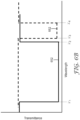
- FIG. 5 is a schematic illustration of a first reflection band 552 of an oriented polymeric multilayer optical film and first and second blocking bands 562a and 562b of one or two non-birefringent optical filters, all at normal incidence.
- the first reflection band 552 and the first and second blocking bands 562a and 562b shift with incidence angle such that both of the first and second blocking bands 562a and 562b overlap with band edges of the first reflection band 552 at an oblique incidence angle (e.g., 45 or 60 degrees).
- the first reflection band 552 and the first and second blocking bands 562a and 562b shift with incidence angle such that one or both of the first and second blocking bands 562a and 562b do not overlap with band edges of the first reflection band 552 at an oblique incidence angle (e.g., 45 or 60 degrees).
- one or both of the first and second blocking bands 562a and 562b do not overlap with a band edge of the first reflection band 552 at normal incidence, but do overlap with a band edge of the first reflection band 552 at an oblique incidence angle.
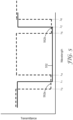
- FIGS. 6A-6B schematically illustrates first reflection band 652 and first blocking band 662 which overlap at normal incidence (shown in FIG. 6A ) and which do not overlap at an oblique incidence angle (shown in FIG. 6B ).
- the first reflection band 652 has band edges at ⁇ 1 and at normal incidence and at ⁇ ' 1 and ⁇ ' 2 , respectively, at the oblique incidence angle.
- the first blocking band 662 has band edges at ⁇ 3 and ⁇ 4 at normal incidence and at ⁇ ' 3 and ⁇ ' 4 , respectively, at the oblique incidence angle.
- a passband is present between ⁇ ' 2 and ⁇ ' 3 at the oblique incidence angle.
- the oblique incidence angle may be 45 degrees or 60 degrees, for example.
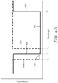
- FIGS. 7A-7B schematically illustrates first reflection band 752 and first blocking band 762 which do not overlap at normal incidence (shown in FIG. 7A ) and which do overlap at an oblique incidence angle (shown in FIG. 7B ).
- the first reflection band 752 has band edges at ⁇ 1 and ⁇ 2 at normal incidence and at ⁇ ' 1 and ⁇ ' 2 , respectively, at the oblique incidence angle.
- the first blocking band 762 has band edges at ⁇ 3 and ⁇ 4 at normal incidence and at ⁇ ' 3 and ⁇ ' 4 , respectively, at the oblique incidence angle.
- a passband is present between ⁇ 4 and ⁇ 1 at normal incidence which is not present at the oblique incidence angle.
- the oblique incidence angle may be 45 degrees or 60 degrees, for example.
- the blocking band partially overlaps the reflection band at normal incidence and extends to the right of a right band edge of the reflection band at normal incidence.
- the relative shifts of the band edges can be selected such that the band width of the resulting overall blocking band of the optical stack narrows with increasing incidence angle.
- the blocking band partially overlaps the reflection band at normal incidence and extends to the left of a left band edge of the reflection band at normal incidence.
- the relative shifts of the band edges can be selected such that the band width of the resulting overall blocking band of the optical stack widens with incidence angle and/or opens a passband (e.g., a passband between ⁇ " 4 and ⁇ " 1 is present in FIG. 4C ).
- the blocking band at least partially overlaps the reflection band at normal incidence and does not extend beyond the reflection band at normal incidence.
- the relative shifts of the band edges can be selected such that the overall blocking band expands and/or opens a passband (for example the wavelength range from ⁇ ' 2 to ⁇ ' 3 depicted in FIG. 6B is a passband where transmission is allowed; this passband is not present in FIG.
- the blocking band does not overlap the reflection band at normal incidence and is positioned to the left of the left band edge of the reflection band.
- the relative shifts of the band edges can be selected such that the overall blocking band narrows and/or a passband narrows or closes (for example the wavelength range from ⁇ 4 to ⁇ 1 depicted in FIG. 7A is a passband where transmission is allowed; this passband is closed in FIG. 7B ).
- the blocking band does not overlap the reflection band at normal incidence and is positioned to the right of the right band edge of the reflection band.
- the relative shifts of the band edges can be selected such that a passband between the reflection band and the blocking band widens with increasing incidence angle.
- the oriented polymeric multilayer optical film has a plurality of reflection bands. In some examples not encompassed by the wording of the claims, the oriented polymeric multilayer optical film is a comb filter having a plurality of passbands between adjacent reflection bands. In some examples not encompassed by the wording of the claims, at least some of the passbands shift under the blocking band or shift out from under the blocking band as the angle of incidence varies.
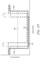
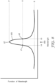
- FIG. 8 is a graph illustrating the concept of full-width at half-maximum ("FWHM").
- the curve 850 represents a function of wavelength that can correspond to a transmittance, 1 minus a transmittance, an absorbance, a reflectance, an output spectrum of a light source, or an input spectrum of a sensor, for example.
- a baseline value B of the curve 850, a peak value P of the curve 850, and an intermediate value H of the curve 850, halfway between P and B are identified in FIG. 8 .
- the curve 850 intersects with the value H at the points p1 and p2, whose wavelength values equal the short wavelength band edge ⁇ a and the long wavelength band edge ⁇ b, respectively, of the band 869.
- the short and long wavelength band edges can be used to calculate two other parameters of interest: the width (full-width at half-maximum, or "FWHM") of the band 869, which equals ⁇ b - ⁇ a; and the center wavelength of the band 869, which equals ( ⁇ a+ ⁇ b)/2.
- the center wavelength may be the same as or different from the peak wavelength (point p3) of the band 869, depending on how symmetrical or asymmetrical the curve 850 is.
- the curve 850 represents 1 minus the transmittance through a non-birefringent optical filter or through an oriented polymeric multilayer optical film. In some examples not encompassed by the wording of the claims, the curve 850 represents an output band of a light source. In some examples not encompassed by the wording of the claims, the curve 850 represents an input band for a sensor.
- the value H may be greater than 0.6 (transmittance no more than 0.4 or 40 percent), greater than 0.7 (transmittance no more than 0.3 or 30 percent), greater than 0.8 (transmittance no more than 0.2 or 20 percent), or greater than 0.9 (transmittance no more than 0.1 or 10 percent).
- the value P may be greater than 0.7 (transmittance no more than 0.3 or 30 percent), greater than 0.8 (transmittance no more than 0.2 or 20 percent), or greater than 0.9 (transmittance no more than 0.1 or 10 percent).
- the value B may be less than 0.5 (transmittance at least 0.5 or 50 percent), less than 0.4 (transmittance at least 0.6 or 60 percent), less than 0.3 (transmittance at least 0.7 or 70 percent), or less than 0.2 (transmittance at least 0.8 or 80 percent).
- FIG. 9 is a cross-sectional view of filter 913 which includes a plurality of alternating first layers 957 and second layers 959.
- Filter 913 can be an oriented polymeric multilayer optical film or a non-birefringent optical filter depending on the selection of the first and second layers 957 and 959.
- the alternating first and second layers 957 and 959 are alternating polymeric layers having different refractive indices.
- the alternating first and second layers 957 and 959 are alternating polymeric layers where at least one of the first and second layers 957 and 959 are oriented polymeric layers.
- Such polymeric filters e.g., mirrors or reflective polarizers
- a polymeric multilayer optical film can be made by coextruding a plurality of alternating polymeric layers (e.g., hundreds of layers), uniaxially or substantially uniaxially stretching the extruded film (e.g., in a linear or parabolic tenter) to orient the film in the case of a polarizer or biaxially stretching the film to orient the film in the case of a mirror.
- a non-birefringent optical filter used in an optical stack is formed by depositing an absorbing material (e.g., by one or more of printing, spraying, and laminating the absorbing material) onto a separate substrate or directly onto the oriented polymeric multilayer optical film. If a separate substrate is used, after depositing the non-birefringent optical filter onto the substrate, the substrate can optionally be laminated to the oriented polymeric multilayer optical film.
- the alternating first and second layers 957 and 959 are alternating non-birefringent layers.
- the alternating non-birefringent layers can be deposited onto a substrate and the substrate positioned adjacent to (and optionally laminated to) an oriented polymeric multilayer optical film for form an optical stack, or the alternating non-birefringent layers can be deposited directly onto an oriented polymeric multilayer optical film for form an optical stack.
- the alternating non-birefringent layers is deposited using one or more of atomic layer deposition, sputtering, chemical vapor deposition, and layer-by-layer self-assembly.
- the alternating first and second layers 957 and 959 are alternating inorganic layers.
- the filter 913 may be referred to as a dielectric mirror.
- dielectric mirrors can be made by depositing alternate low and high index layers of inorganic materials using thin-film deposition techniques known in the art. For example, alternating layers of TiO 2 and SiO 2 can be evaporated onto a substrate or onto an oriented multilayer optical film to provide a reflective non-birefringent optical filter.
- Other oxides or metal-doped oxides can also be used, including, for example, zinc oxide or metal-doped zinc oxide, and metal-doped silicon oxide.
- Al-doped ZnO or Al-doped SiO x can be used as inorganic layers.
- one of the alternating first and second layers 957 and 959 is polymeric and the other of the alternating first and second layers 957 and 959 is inorganic.
- an inorganic second layer 959 can be vapor deposited or sputtered onto a polymeric first layer 957, then another polymeric first layer 957 can be coated onto the inorganic second layer 959.
- Another inorganic second layer 959 can then be deposited onto the coated polymeric first layer 957 and the process repeated until a desired number of layers is formed.
- the polymeric first layers can be formed using a vacuum coater similar to the coater described in U.S. Pat. No. 5,440,446 (Shaw et al. ) and U.S.
- Pat. No. 7,018,713 (Padiyath et al ). to deposit a monomer layer and curing the monomer layer by exposure to actinic radiation (e.g., ultra-violet radiation).
- actinic radiation e.g., ultra-violet radiation
- a stack of alternating layers of cured acrylate polymer (e.g., having a refractive index in a range of 1.4 to 1.6) and an oxide (e.g., a metal oxide having a refractive index in a range of 1.8 to 3.0) can be used to provide a reflective non-birefringent optical filter.
- the oxide can be a metal-doped oxide such as Al-doped ZnO.
- Refractive index can refer to the refractive index determined at a wavelength of a center of a desired reflection band or at a standard fixed wavelength such as 550 nm, for example.
- a filter 913 having alternating inorganic layers and a different filter 913 having alternating oriented polymeric layers are placed adjacent each other to form an optical stack of the present description.
- the two filters can be laminated together through an adhesive layer or the inorganic filter can be deposited layer by layer onto the polymeric filter using the layer-by-layer self-assembly methods of U.S. Pat. Pub. No. 2015/0285956 (Schmidt et al. ).
- reflection is provided when a pair of adjacent layers (optical repeat unit) has a total optical thickness (physical thickness of a layer times the refractive index of the layer) of half of a wavelength.
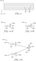
- FIG. 10A is a schematic illustration of optical system 1001a including light source 1022 and optical filter 1000a.
- a light ray 1040a is emitted by the light source 1022 and transmitted through optical filter 1000a.
- Optical filter 1000a may be any of the optical stacks of the present description or may be an oriented polymeric multilayer optical film having a first reflection band with a first band edge.
- FIG. 10B is a schematic illustration of optical system 1001b including sensor 1024 and optical filter 1000b.
- a light ray 1040b is transmitted through optical filter 1000b and is received by the sensor 1024.
- Optical filter 1000b may be any of the optical stacks of the present description or may be an oriented polymeric multilayer optical film having a first reflection band with a first band edge.
- Optical filter 1000b may be configured to limit light transmitted into the sensor 1024 to a desired input band for the sensor 1024.
- an optical system includes both a light source and a sensor.
- a light source may be included in optical system 1001b disposed to provide the light ray 1040b which may reflect off of a marker (e.g., a white tee shirt, reflective tape, markers in a sign, license plates such as retroreflective license plates, etc.) before passing through optical filter 1000b or a sensor may be included in optical system 1000a to receive the light ray 1040a directly or after the light ray 1040a has reflected off of a marker, for example.
- a marker e.g., a white tee shirt, reflective tape, markers in a sign, license plates such as retroreflective license plates, etc.
- the optical stacks of the present description are used to provide angular limitations of light passing through the filter.
- an optical stack can block light emitted by a light source at normal incidence and transmit light of the same wavelength at an oblique incidence angle.
- an optical stack can transmit light emitted by a light source at normal incidence and block light of the same wavelength at an oblique incidence angle.
- FIG. 10C is a schematic illustration of optical system 1001c which includes the optical systems 1001a and 1001b described in reference to FIGS. 10A-B and which further includes marker 1030 which is in optical communication with light source 1022 and sensor 1024.
- Marker 1030 includes reflector 1032 and layer 1034.
- Reflector 1032 may be or may include one or more of a specular reflector, a diffuse reflector, a semi-specular reflector, and a retroreflector.
- Layer 1034 can be an optical filter suitable for a given application, for example.
- layer 1034 is an optical stack of the present description, which can be used, for example, as an angle limiting filter for the marker 1030. In other embodiments, layer 1034 is omitted.
- an optical system which includes an optical filter and further includes one or both of a light source and a sensor in optical communication with the optical filter.
- the optical filter may be any of the optical stacks of the present description or may be an oriented polymeric multilayer optical film having a first reflection band with a first band edge.
- the optical system includes the light source which may be configured to produce light in an output band.
- the output band is a narrow band (e.g., a band having a full-width at half-maximum of no more than 40 nm).
- the light source is a light emitting diode (LED), a laser, or a laser diode, for example.
- the optical system includes the sensor which may be configured to receive light in an input band.
- the input band is a narrow band (e.g., a band having a full-width at half-maximum of no more than 40 nm) which may be established by an optical bandpass filter disposed at an entrance to the sensor.
- the first reflection band of the optical stack overlaps the output band and/or the input band at normal incidence, but not at an oblique incidence angle (e.g., 45 or 60 degrees).
- the first reflection band may correspond to reflection band 652 and the output band and/or the input band may be in a wavelength range of ⁇ 3 to ⁇ 4 depicted in FIG. 6A .
- the range of ⁇ 3 to ⁇ 4 overlaps the range of ⁇ 1 to ⁇ 2 and at an oblique incidence angle, the range of ⁇ 3 to ⁇ 4 does not overlap the range of ⁇ ' 1 to ⁇ ' 2 .
- the first reflection band overlaps the output band and/or the input band an oblique incidence angle (e.g., 45 or 60 degrees), but not at normal incidence.
- the first reflection band may correspond to reflection band 752 and the output band and/or input band may be in a wavelength range of ⁇ 3 to ⁇ 4 depicted in FIG. 7A .
- the optical system includes both the light source and the sensor where the sensor, the light source and the optical stack are in optical communication with each other as described further elsewhere herein.
- Optical spectra for were measured using a Perkin Elmer Lambda 900 UV/VIS spectrophotometer.
- An oriented polymeric multilayer optical film was prepared as generally described in U.S. Pat. Nos. 5,882,774 (Jonza et al. ).
- the film included a single multilayer optical packet comprised of 550 alternating layers of high index layers of polyethylene naphthalate (PEN) and low index layers of polymethylmethacrylate (PMMA), and included a protective skin layer of PEN on each side, for a total of 552 layers.
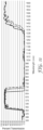
- the film was extruded and biaxially stretched to produce an oriented polymeric multilayer optical film having the optical spectra shown in FIG. 11 at normal incidence.
- the optical spectra shown in FIG. 11 includes data taken from multiple sections of the film overlaid to demonstrate the result of process variations.
- the optical band edge was at ⁇ 700 nm and cross-web variation was on the order of 50 nm.
- An oriented polymeric multilayer optical film was prepared as described generally for Preparatory Example 1.
- the film was extruded and biaxially stretched to produce an oriented polymeric multilayer optical film having the optical spectra shown in FIG. 12 .
- the optical spectra shown in FIG. 12 includes film data taken at multiple locations which are overlaid to demonstrate the result of process variations.
- the curves labeled C1, C3, C8, C11, C17 and C24 correspond to crossweb positions across the film a 2.8 inches, 4.7, inches, 13.8 inches, 19.3 inches, 30.3 inches and 43.2 inches from an end of the film.
- the optical band edge was at ⁇ 800 nm and cross-web variation was on the order of 50 nm.
- a non-birefringent band edge correction filter in the form of a hybrid organic/inorganic interference filter was deposited using the vacuum deposition procedures generally described in U.S. Pat. No. 7,018,713 (Padiyath et al. ).
- the hybrid filter was deposited onto a PET film substrate and subsequently laminated onto the multilayer optical film stack described as Preparatory Example 1 to produce an optical stack.
- the hybrid filter could have been directly coated onto the multilayer optical film stack of Preparatory Example 1.
- the optical spectra of this hybrid non-birefringent correction filter are shown in FIG. 13 .
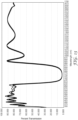
- the same hybrid filter formed on PET that was used for Example 1 was laminated onto the oriented polymeric multilayer optical film of Preparatory Example 2 to produce an optical stack.
- the resulting optical spectra was measured with results displayed in FIG. 15 .
- the curves labeled L1, L3, L8, L11, L17 and L24 correspond to C1, C3, C8, C11, C17 and C24, respectively, of FIG. 12 .
- the resulting measurements showed the band edge wavelength to shift to that of the hybrid filter at ⁇ 660nm with cross-web variation reduced from ⁇ 50 nm to less than 5 nm.
- This Example demonstrates the use of an absorptive dye layer to provide correction to band edge of a multilayer optical film.
- An oriented polymeric multilayer optical film was produce as in Preparatory Example 1 and had the spectra shown in FIG. 16 (and also shown as curve 1882 in FIG. 18 ).
- a sample of 1/8" thick Acrylite 257-0 GP Red (Cyro Corporation) was used as a non-birefringent optical filter.
- This material contained a spectrally sharp absorbing dye in an acrylic host as shown in the transmission spectrum of FIG. 17 (also shown as curve 1884 in FIG. 18 ). It absorbs heavily below about 610 nm, and has a sharp transition to high transmission at higher wavelengths.
- the Acrylite 257-0 GP Red layer was placed adjacent the oriented polymeric multilayer optical film to produce an optical stack which was a notch filter at normal incidence with a passband 1860 having peak transmission at about 640 nm with a full-width half-maximum of about 55 nm as shown in FIG. 18 . Since the absorber band edge does not shift with incidence angle and the oriented polymeric multilayer optical film interference filter shifts to lower wavelengths with increasing incidence angle, the transmission notch closes quickly as a function of angle. Transmission through the optical stack was observed to shift from red to black as the angle of incidence changed from normal to about 30 degrees.
Landscapes
- Physics & Mathematics (AREA)
- General Physics & Mathematics (AREA)
- Optics & Photonics (AREA)
- Optical Filters (AREA)
- Polarising Elements (AREA)
Applications Claiming Priority (2)
| Application Number | Priority Date | Filing Date | Title |
|---|---|---|---|
| US201662361246P | 2016-07-12 | 2016-07-12 | |
| PCT/US2017/040290 WO2018013363A1 (en) | 2016-07-12 | 2017-06-30 | Optical stack |
Publications (3)
| Publication Number | Publication Date |
|---|---|
| EP3485303A1 EP3485303A1 (en) | 2019-05-22 |
| EP3485303A4 EP3485303A4 (en) | 2020-05-06 |
| EP3485303B1 true EP3485303B1 (en) | 2024-02-14 |
Family
ID=60953293
Family Applications (1)
| Application Number | Title | Priority Date | Filing Date |
|---|---|---|---|
| EP17828181.2A Active EP3485303B1 (en) | 2016-07-12 | 2017-06-30 | Optical stack |
Country Status (7)
| Country | Link |
|---|---|
| US (2) | US11009637B2 (enExample) |
| EP (1) | EP3485303B1 (enExample) |
| JP (1) | JP7099786B2 (enExample) |
| KR (1) | KR20190018550A (enExample) |
| CN (1) | CN109477920B (enExample) |
| TW (1) | TW201821260A (enExample) |
| WO (1) | WO2018013363A1 (enExample) |
Families Citing this family (9)
| Publication number | Priority date | Publication date | Assignee | Title |
|---|---|---|---|---|
| CN111684337B (zh) * | 2018-02-09 | 2022-04-26 | 三菱电机株式会社 | 光合分波器的制造方法 |
| KR20210042929A (ko) * | 2018-08-15 | 2021-04-20 | 쓰리엠 이노베이티브 프로퍼티즈 컴파니 | 마이크로렌즈 어레이를 포함하는 광학 요소 |
| TWI705269B (zh) * | 2019-03-27 | 2020-09-21 | 群光電子股份有限公司 | 影像擷取裝置、濾光膜及濾光膜的製作方法 |
| CN114041074B (zh) * | 2019-07-02 | 2024-08-20 | 3M创新有限公司 | 包括具有降频转换器的波长选择性光学滤光器的光学装置 |
| KR20220113707A (ko) * | 2019-12-09 | 2022-08-16 | 쓰리엠 이노베이티브 프로퍼티즈 컴파니 | 광학 필터 및 광학 시스템 |
| WO2022027589A1 (en) * | 2020-08-07 | 2022-02-10 | 3M Innovative Properties Company | Optical stack and housing for electronic device |
| WO2022058812A1 (en) * | 2020-09-15 | 2022-03-24 | 3M Innovative Properties Company | Display and optical film |
| CN117597605A (zh) * | 2021-06-29 | 2024-02-23 | 3M创新有限公司 | 包括角度控制膜的光学系统 |
| WO2023218633A1 (ja) * | 2022-05-13 | 2023-11-16 | オリンパスメディカルシステムズ株式会社 | 撮像ユニット、内視鏡、および、撮像ユニットの製造方法 |
Family Cites Families (35)
| Publication number | Priority date | Publication date | Assignee | Title |
|---|---|---|---|---|
| DE69325283T2 (de) * | 1992-10-29 | 1999-11-04 | Minnesota Mining & Mfg | Formbarer reflektierender multischichtenkörper |
| US5510173A (en) * | 1993-08-20 | 1996-04-23 | Southwall Technologies Inc. | Multiple layer thin films with improved corrosion resistance |
| US5440446A (en) | 1993-10-04 | 1995-08-08 | Catalina Coatings, Inc. | Acrylate coating material |
| US5882774A (en) | 1993-12-21 | 1999-03-16 | Minnesota Mining And Manufacturing Company | Optical film |
| ES2173153T3 (es) * | 1994-04-12 | 2002-10-16 | Jax Holdings Inc | Dispositivo de filtro optico. |
| DE69709053T2 (de) * | 1997-04-17 | 2002-07-18 | Asulab S.A., Biel/Bienne | Flüssigkristallanzeige-Vorrichtung für einen farbigen Bildschirm |
| US6049419A (en) | 1998-01-13 | 2000-04-11 | 3M Innovative Properties Co | Multilayer infrared reflecting optical body |
| US6531230B1 (en) | 1998-01-13 | 2003-03-11 | 3M Innovative Properties Company | Color shifting film |
| US6157486A (en) | 1998-01-13 | 2000-12-05 | 3M Innovative Properties Company | Retroreflective dichroic reflector |
| EP1074863B1 (fr) | 1999-08-04 | 2015-03-04 | Asulab S.A. | Dispositif optique à réflexion de Bragg et procédés pour sa fabrication |
| US6506480B2 (en) * | 2001-02-16 | 2003-01-14 | 3M Innovative Properties Company | Color shifting film with a plurality of fluorescent colorants |
| US6916440B2 (en) | 2001-05-31 | 2005-07-12 | 3M Innovative Properties Company | Processes and apparatus for making transversely drawn films with substantially uniaxial character |
| US7095009B2 (en) | 2002-05-21 | 2006-08-22 | 3M Innovative Properties Company | Photopic detector system and filter therefor |
| MXPA05003106A (es) * | 2002-09-20 | 2005-06-22 | Honeywell Int Inc | Pantalla de visualizacion de alta eficiencia. |
| US6936209B2 (en) | 2002-11-27 | 2005-08-30 | 3M Innovative Properties Company | Methods and devices for processing polymer films |
| US6949212B2 (en) | 2002-11-27 | 2005-09-27 | 3M Innovative Properties Company | Methods and devices for stretching polymer films |
| US7064897B2 (en) * | 2002-12-31 | 2006-06-20 | 3M Innovative Properties Company | Optical polarizing films with designed color shifts |
| US7018713B2 (en) | 2003-04-02 | 2006-03-28 | 3M Innovative Properties Company | Flexible high-temperature ultrabarrier |
| JP2006523955A (ja) | 2003-04-08 | 2006-10-19 | スリーエム イノベイティブ プロパティズ カンパニー | 可視波長検出器システムおよびそのためのフィルタ |
| US20070097509A1 (en) * | 2005-10-31 | 2007-05-03 | Nevitt Timothy J | Optical elements for high contrast applications |
| BRPI0721299B1 (pt) | 2006-12-28 | 2018-07-24 | 3M Innovative Properties Company. | Método para formação de um filme condutivo em um suporte de polímero flexível, filme condutivo e método para a fabricação de um artigo de vitrificação |
| CN101909873B (zh) | 2007-12-28 | 2016-10-19 | 3M创新有限公司 | 用于阳光控制及其它用途的红外线反射膜 |
| US8350451B2 (en) | 2008-06-05 | 2013-01-08 | 3M Innovative Properties Company | Ultrathin transparent EMI shielding film comprising a polymer basecoat and crosslinked polymer transparent dielectric layer |
| US8314991B2 (en) * | 2008-10-31 | 2012-11-20 | Cpfilms Inc. | Variable transmission composite interference filter |
| US9097858B2 (en) * | 2010-06-30 | 2015-08-04 | 3M Innovative Properties Company | Retarder film combinations with spatially selective birefringence reduction |
| JP5796432B2 (ja) | 2010-09-22 | 2015-10-21 | 東レ株式会社 | 成型体及び電子機器 |
| JP2015531883A (ja) * | 2012-06-28 | 2015-11-05 | コーロン インダストリーズ インク | 輝度増強フィルム及びこれを含むバックライトユニット |
| US9829604B2 (en) | 2012-12-20 | 2017-11-28 | 3M Innovative Properties Company | Method of making multilayer optical film comprising layer-by-layer self-assembled layers and articles |
| US10054803B2 (en) * | 2013-01-14 | 2018-08-21 | 3M Innovative Properties Company | Filters to enhance color discrimination for color vision deficient individuals |
| EP3042226A1 (en) * | 2013-09-06 | 2016-07-13 | 3M Innovative Properties Company | Multilayer reflective polarizer |
| EP3072000B1 (en) * | 2013-11-19 | 2024-05-22 | 3M Innovative Properties Company | Multilayer polymeric reflector |
| US9885885B2 (en) | 2013-11-27 | 2018-02-06 | 3M Innovative Properties Company | Blue edge filter optical lens |
| EP3114521A1 (en) * | 2014-03-07 | 2017-01-11 | 3M Innovative Properties Company | Light source incorporating multilayer optical film |
| US9823395B2 (en) * | 2014-10-17 | 2017-11-21 | 3M Innovative Properties Company | Multilayer optical film having overlapping harmonics |
| KR20190007442A (ko) | 2016-06-09 | 2019-01-22 | 쓰리엠 이노베이티브 프로퍼티즈 컴파니 | 광학 필터 |
-
2017
- 2017-06-30 US US16/309,187 patent/US11009637B2/en active Active
- 2017-06-30 KR KR1020197003956A patent/KR20190018550A/ko not_active Withdrawn
- 2017-06-30 EP EP17828181.2A patent/EP3485303B1/en active Active
- 2017-06-30 JP JP2019501561A patent/JP7099786B2/ja active Active
- 2017-06-30 WO PCT/US2017/040290 patent/WO2018013363A1/en not_active Ceased
- 2017-06-30 CN CN201780043208.3A patent/CN109477920B/zh active Active
- 2017-07-11 TW TW106123133A patent/TW201821260A/zh unknown
-
2021
- 2021-04-09 US US17/226,265 patent/US20210231851A1/en not_active Abandoned
Also Published As
| Publication number | Publication date |
|---|---|
| WO2018013363A1 (en) | 2018-01-18 |
| JP7099786B2 (ja) | 2022-07-12 |
| US20210231851A1 (en) | 2021-07-29 |
| KR20190018550A (ko) | 2019-02-22 |
| JP2019523444A (ja) | 2019-08-22 |
| TW201821260A (zh) | 2018-06-16 |
| US11009637B2 (en) | 2021-05-18 |
| US20190331837A1 (en) | 2019-10-31 |
| EP3485303A1 (en) | 2019-05-22 |
| EP3485303A4 (en) | 2020-05-06 |
| CN109477920A (zh) | 2019-03-15 |
| CN109477920B (zh) | 2022-02-08 |
Similar Documents
| Publication | Publication Date | Title |
|---|---|---|
| EP3485303B1 (en) | Optical stack | |
| CN113608292B (zh) | 光学膜 | |
| US11016229B2 (en) | Optical filter | |
| US9678252B2 (en) | Multilayer stack with overlapping harmonics for wide visible-infrared coverage | |
| KR101971754B1 (ko) | 상이한 광학 패킷들을 갖는 아포다이징된 광대역 부분 반사기 | |
| CN114280717B (zh) | 用于校正色移的部分反射器、圆形偏振片及显示器 | |
| JP6576913B2 (ja) | 多層光学フィルム | |
| RU2512089C2 (ru) | Составной интерференционный фильтр с изменяемым пропусканием | |
| US20210215865A1 (en) | Optical system and optical film | |
| US11947138B2 (en) | Broadband visible reflector | |
| JP7676399B2 (ja) | 光学フィルタ及び光学システム | |
| JP2020521166A (ja) | 可撓性の超薄型ハイブリッド吸収性‐反射性薄膜フィルタおよびその作製方法 |
Legal Events
| Date | Code | Title | Description |
|---|---|---|---|
| STAA | Information on the status of an ep patent application or granted ep patent |
Free format text: STATUS: THE INTERNATIONAL PUBLICATION HAS BEEN MADE |
|
| PUAI | Public reference made under article 153(3) epc to a published international application that has entered the european phase |
Free format text: ORIGINAL CODE: 0009012 |
|
| STAA | Information on the status of an ep patent application or granted ep patent |
Free format text: STATUS: REQUEST FOR EXAMINATION WAS MADE |
|
| 17P | Request for examination filed |
Effective date: 20190122 |
|
| AK | Designated contracting states |
Kind code of ref document: A1 Designated state(s): AL AT BE BG CH CY CZ DE DK EE ES FI FR GB GR HR HU IE IS IT LI LT LU LV MC MK MT NL NO PL PT RO RS SE SI SK SM TR |
|
| AX | Request for extension of the european patent |
Extension state: BA ME |
|
| DAV | Request for validation of the european patent (deleted) | ||
| DAX | Request for extension of the european patent (deleted) | ||
| A4 | Supplementary search report drawn up and despatched |
Effective date: 20200403 |
|
| RIC1 | Information provided on ipc code assigned before grant |
Ipc: G02B 5/22 20060101ALI20200330BHEP Ipc: G02B 5/28 20060101ALI20200330BHEP Ipc: G02B 5/26 20060101AFI20200330BHEP |
|
| STAA | Information on the status of an ep patent application or granted ep patent |
Free format text: STATUS: EXAMINATION IS IN PROGRESS |
|
| 17Q | First examination report despatched |
Effective date: 20220802 |
|
| GRAP | Despatch of communication of intention to grant a patent |
Free format text: ORIGINAL CODE: EPIDOSNIGR1 |
|
| STAA | Information on the status of an ep patent application or granted ep patent |
Free format text: STATUS: GRANT OF PATENT IS INTENDED |
|
| INTG | Intention to grant announced |
Effective date: 20230929 |
|
| GRAS | Grant fee paid |
Free format text: ORIGINAL CODE: EPIDOSNIGR3 |
|
| GRAA | (expected) grant |
Free format text: ORIGINAL CODE: 0009210 |
|
| STAA | Information on the status of an ep patent application or granted ep patent |
Free format text: STATUS: THE PATENT HAS BEEN GRANTED |
|
| AK | Designated contracting states |
Kind code of ref document: B1 Designated state(s): AL AT BE BG CH CY CZ DE DK EE ES FI FR GB GR HR HU IE IS IT LI LT LU LV MC MK MT NL NO PL PT RO RS SE SI SK SM TR |
|
| REG | Reference to a national code |
Ref country code: GB Ref legal event code: FG4D |
|
| REG | Reference to a national code |
Ref country code: CH Ref legal event code: EP |
|
| REG | Reference to a national code |
Ref country code: DE Ref legal event code: R096 Ref document number: 602017079201 Country of ref document: DE |
|
| REG | Reference to a national code |
Ref country code: IE Ref legal event code: FG4D |
|
| P01 | Opt-out of the competence of the unified patent court (upc) registered |
Effective date: 20240226 |
|
| REG | Reference to a national code |
Ref country code: LT Ref legal event code: MG9D |
|
| REG | Reference to a national code |
Ref country code: NL Ref legal event code: MP Effective date: 20240214 |
|
| PG25 | Lapsed in a contracting state [announced via postgrant information from national office to epo] |
Ref country code: IS Free format text: LAPSE BECAUSE OF FAILURE TO SUBMIT A TRANSLATION OF THE DESCRIPTION OR TO PAY THE FEE WITHIN THE PRESCRIBED TIME-LIMIT Effective date: 20240614 |
|
| PG25 | Lapsed in a contracting state [announced via postgrant information from national office to epo] |
Ref country code: LT Free format text: LAPSE BECAUSE OF FAILURE TO SUBMIT A TRANSLATION OF THE DESCRIPTION OR TO PAY THE FEE WITHIN THE PRESCRIBED TIME-LIMIT Effective date: 20240214 |
|
| PG25 | Lapsed in a contracting state [announced via postgrant information from national office to epo] |
Ref country code: GR Free format text: LAPSE BECAUSE OF FAILURE TO SUBMIT A TRANSLATION OF THE DESCRIPTION OR TO PAY THE FEE WITHIN THE PRESCRIBED TIME-LIMIT Effective date: 20240515 |
|
| REG | Reference to a national code |
Ref country code: AT Ref legal event code: MK05 Ref document number: 1657502 Country of ref document: AT Kind code of ref document: T Effective date: 20240214 |
|
| PG25 | Lapsed in a contracting state [announced via postgrant information from national office to epo] |
Ref country code: RS Free format text: LAPSE BECAUSE OF FAILURE TO SUBMIT A TRANSLATION OF THE DESCRIPTION OR TO PAY THE FEE WITHIN THE PRESCRIBED TIME-LIMIT Effective date: 20240514 Ref country code: NL Free format text: LAPSE BECAUSE OF FAILURE TO SUBMIT A TRANSLATION OF THE DESCRIPTION OR TO PAY THE FEE WITHIN THE PRESCRIBED TIME-LIMIT Effective date: 20240214 Ref country code: HR Free format text: LAPSE BECAUSE OF FAILURE TO SUBMIT A TRANSLATION OF THE DESCRIPTION OR TO PAY THE FEE WITHIN THE PRESCRIBED TIME-LIMIT Effective date: 20240214 |
|
| PG25 | Lapsed in a contracting state [announced via postgrant information from national office to epo] |
Ref country code: ES Free format text: LAPSE BECAUSE OF FAILURE TO SUBMIT A TRANSLATION OF THE DESCRIPTION OR TO PAY THE FEE WITHIN THE PRESCRIBED TIME-LIMIT Effective date: 20240214 |
|
| PG25 | Lapsed in a contracting state [announced via postgrant information from national office to epo] |
Ref country code: AT Free format text: LAPSE BECAUSE OF FAILURE TO SUBMIT A TRANSLATION OF THE DESCRIPTION OR TO PAY THE FEE WITHIN THE PRESCRIBED TIME-LIMIT Effective date: 20240214 |
|
| PG25 | Lapsed in a contracting state [announced via postgrant information from national office to epo] |
Ref country code: RS Free format text: LAPSE BECAUSE OF FAILURE TO SUBMIT A TRANSLATION OF THE DESCRIPTION OR TO PAY THE FEE WITHIN THE PRESCRIBED TIME-LIMIT Effective date: 20240514 Ref country code: NO Free format text: LAPSE BECAUSE OF FAILURE TO SUBMIT A TRANSLATION OF THE DESCRIPTION OR TO PAY THE FEE WITHIN THE PRESCRIBED TIME-LIMIT Effective date: 20240514 Ref country code: NL Free format text: LAPSE BECAUSE OF FAILURE TO SUBMIT A TRANSLATION OF THE DESCRIPTION OR TO PAY THE FEE WITHIN THE PRESCRIBED TIME-LIMIT Effective date: 20240214 Ref country code: LT Free format text: LAPSE BECAUSE OF FAILURE TO SUBMIT A TRANSLATION OF THE DESCRIPTION OR TO PAY THE FEE WITHIN THE PRESCRIBED TIME-LIMIT Effective date: 20240214 Ref country code: IS Free format text: LAPSE BECAUSE OF FAILURE TO SUBMIT A TRANSLATION OF THE DESCRIPTION OR TO PAY THE FEE WITHIN THE PRESCRIBED TIME-LIMIT Effective date: 20240614 Ref country code: HR Free format text: LAPSE BECAUSE OF FAILURE TO SUBMIT A TRANSLATION OF THE DESCRIPTION OR TO PAY THE FEE WITHIN THE PRESCRIBED TIME-LIMIT Effective date: 20240214 Ref country code: GR Free format text: LAPSE BECAUSE OF FAILURE TO SUBMIT A TRANSLATION OF THE DESCRIPTION OR TO PAY THE FEE WITHIN THE PRESCRIBED TIME-LIMIT Effective date: 20240515 Ref country code: FI Free format text: LAPSE BECAUSE OF FAILURE TO SUBMIT A TRANSLATION OF THE DESCRIPTION OR TO PAY THE FEE WITHIN THE PRESCRIBED TIME-LIMIT Effective date: 20240214 Ref country code: ES Free format text: LAPSE BECAUSE OF FAILURE TO SUBMIT A TRANSLATION OF THE DESCRIPTION OR TO PAY THE FEE WITHIN THE PRESCRIBED TIME-LIMIT Effective date: 20240214 Ref country code: BG Free format text: LAPSE BECAUSE OF FAILURE TO SUBMIT A TRANSLATION OF THE DESCRIPTION OR TO PAY THE FEE WITHIN THE PRESCRIBED TIME-LIMIT Effective date: 20240214 Ref country code: AT Free format text: LAPSE BECAUSE OF FAILURE TO SUBMIT A TRANSLATION OF THE DESCRIPTION OR TO PAY THE FEE WITHIN THE PRESCRIBED TIME-LIMIT Effective date: 20240214 |
|
| PG25 | Lapsed in a contracting state [announced via postgrant information from national office to epo] |
Ref country code: PT Free format text: LAPSE BECAUSE OF FAILURE TO SUBMIT A TRANSLATION OF THE DESCRIPTION OR TO PAY THE FEE WITHIN THE PRESCRIBED TIME-LIMIT Effective date: 20240614 Ref country code: PL Free format text: LAPSE BECAUSE OF FAILURE TO SUBMIT A TRANSLATION OF THE DESCRIPTION OR TO PAY THE FEE WITHIN THE PRESCRIBED TIME-LIMIT Effective date: 20240214 |
|
| PG25 | Lapsed in a contracting state [announced via postgrant information from national office to epo] |
Ref country code: SE Free format text: LAPSE BECAUSE OF FAILURE TO SUBMIT A TRANSLATION OF THE DESCRIPTION OR TO PAY THE FEE WITHIN THE PRESCRIBED TIME-LIMIT Effective date: 20240214 Ref country code: PT Free format text: LAPSE BECAUSE OF FAILURE TO SUBMIT A TRANSLATION OF THE DESCRIPTION OR TO PAY THE FEE WITHIN THE PRESCRIBED TIME-LIMIT Effective date: 20240614 Ref country code: PL Free format text: LAPSE BECAUSE OF FAILURE TO SUBMIT A TRANSLATION OF THE DESCRIPTION OR TO PAY THE FEE WITHIN THE PRESCRIBED TIME-LIMIT Effective date: 20240214 Ref country code: LV Free format text: LAPSE BECAUSE OF FAILURE TO SUBMIT A TRANSLATION OF THE DESCRIPTION OR TO PAY THE FEE WITHIN THE PRESCRIBED TIME-LIMIT Effective date: 20240214 |
|
| PG25 | Lapsed in a contracting state [announced via postgrant information from national office to epo] |
Ref country code: DK Free format text: LAPSE BECAUSE OF FAILURE TO SUBMIT A TRANSLATION OF THE DESCRIPTION OR TO PAY THE FEE WITHIN THE PRESCRIBED TIME-LIMIT Effective date: 20240214 |
|
| PG25 | Lapsed in a contracting state [announced via postgrant information from national office to epo] |
Ref country code: SM Free format text: LAPSE BECAUSE OF FAILURE TO SUBMIT A TRANSLATION OF THE DESCRIPTION OR TO PAY THE FEE WITHIN THE PRESCRIBED TIME-LIMIT Effective date: 20240214 |
|
| PG25 | Lapsed in a contracting state [announced via postgrant information from national office to epo] |
Ref country code: CZ Free format text: LAPSE BECAUSE OF FAILURE TO SUBMIT A TRANSLATION OF THE DESCRIPTION OR TO PAY THE FEE WITHIN THE PRESCRIBED TIME-LIMIT Effective date: 20240214 Ref country code: EE Free format text: LAPSE BECAUSE OF FAILURE TO SUBMIT A TRANSLATION OF THE DESCRIPTION OR TO PAY THE FEE WITHIN THE PRESCRIBED TIME-LIMIT Effective date: 20240214 |
|
| PG25 | Lapsed in a contracting state [announced via postgrant information from national office to epo] |
Ref country code: SK Free format text: LAPSE BECAUSE OF FAILURE TO SUBMIT A TRANSLATION OF THE DESCRIPTION OR TO PAY THE FEE WITHIN THE PRESCRIBED TIME-LIMIT Effective date: 20240214 |
|
| PG25 | Lapsed in a contracting state [announced via postgrant information from national office to epo] |
Ref country code: SM Free format text: LAPSE BECAUSE OF FAILURE TO SUBMIT A TRANSLATION OF THE DESCRIPTION OR TO PAY THE FEE WITHIN THE PRESCRIBED TIME-LIMIT Effective date: 20240214 Ref country code: SK Free format text: LAPSE BECAUSE OF FAILURE TO SUBMIT A TRANSLATION OF THE DESCRIPTION OR TO PAY THE FEE WITHIN THE PRESCRIBED TIME-LIMIT Effective date: 20240214 Ref country code: RO Free format text: LAPSE BECAUSE OF FAILURE TO SUBMIT A TRANSLATION OF THE DESCRIPTION OR TO PAY THE FEE WITHIN THE PRESCRIBED TIME-LIMIT Effective date: 20240214 Ref country code: EE Free format text: LAPSE BECAUSE OF FAILURE TO SUBMIT A TRANSLATION OF THE DESCRIPTION OR TO PAY THE FEE WITHIN THE PRESCRIBED TIME-LIMIT Effective date: 20240214 Ref country code: DK Free format text: LAPSE BECAUSE OF FAILURE TO SUBMIT A TRANSLATION OF THE DESCRIPTION OR TO PAY THE FEE WITHIN THE PRESCRIBED TIME-LIMIT Effective date: 20240214 Ref country code: CZ Free format text: LAPSE BECAUSE OF FAILURE TO SUBMIT A TRANSLATION OF THE DESCRIPTION OR TO PAY THE FEE WITHIN THE PRESCRIBED TIME-LIMIT Effective date: 20240214 |
|
| REG | Reference to a national code |
Ref country code: DE Ref legal event code: R097 Ref document number: 602017079201 Country of ref document: DE |
|
| PG25 | Lapsed in a contracting state [announced via postgrant information from national office to epo] |
Ref country code: IT Free format text: LAPSE BECAUSE OF FAILURE TO SUBMIT A TRANSLATION OF THE DESCRIPTION OR TO PAY THE FEE WITHIN THE PRESCRIBED TIME-LIMIT Effective date: 20240214 |
|
| PLBE | No opposition filed within time limit |
Free format text: ORIGINAL CODE: 0009261 |
|
| STAA | Information on the status of an ep patent application or granted ep patent |
Free format text: STATUS: NO OPPOSITION FILED WITHIN TIME LIMIT |
|
| PG25 | Lapsed in a contracting state [announced via postgrant information from national office to epo] |
Ref country code: IT Free format text: LAPSE BECAUSE OF FAILURE TO SUBMIT A TRANSLATION OF THE DESCRIPTION OR TO PAY THE FEE WITHIN THE PRESCRIBED TIME-LIMIT Effective date: 20240214 |
|
| 26N | No opposition filed |
Effective date: 20241115 |
|
| PG25 | Lapsed in a contracting state [announced via postgrant information from national office to epo] |
Ref country code: MC Free format text: LAPSE BECAUSE OF FAILURE TO SUBMIT A TRANSLATION OF THE DESCRIPTION OR TO PAY THE FEE WITHIN THE PRESCRIBED TIME-LIMIT Effective date: 20240214 |
|
| REG | Reference to a national code |
Ref country code: CH Ref legal event code: PL |
|
| PG25 | Lapsed in a contracting state [announced via postgrant information from national office to epo] |
Ref country code: LU Free format text: LAPSE BECAUSE OF NON-PAYMENT OF DUE FEES Effective date: 20240630 |
|
| GBPC | Gb: european patent ceased through non-payment of renewal fee |
Effective date: 20240630 |
|
| PG25 | Lapsed in a contracting state [announced via postgrant information from national office to epo] |
Ref country code: IE Free format text: LAPSE BECAUSE OF NON-PAYMENT OF DUE FEES Effective date: 20240630 |
|
| PG25 | Lapsed in a contracting state [announced via postgrant information from national office to epo] |
Ref country code: SI Free format text: LAPSE BECAUSE OF FAILURE TO SUBMIT A TRANSLATION OF THE DESCRIPTION OR TO PAY THE FEE WITHIN THE PRESCRIBED TIME-LIMIT Effective date: 20240214 Ref country code: CH Free format text: LAPSE BECAUSE OF NON-PAYMENT OF DUE FEES Effective date: 20240630 Ref country code: BE Free format text: LAPSE BECAUSE OF NON-PAYMENT OF DUE FEES Effective date: 20240630 |
|
| PG25 | Lapsed in a contracting state [announced via postgrant information from national office to epo] |
Ref country code: FR Free format text: LAPSE BECAUSE OF NON-PAYMENT OF DUE FEES Effective date: 20240630 |
|
| PG25 | Lapsed in a contracting state [announced via postgrant information from national office to epo] |
Ref country code: GB Free format text: LAPSE BECAUSE OF NON-PAYMENT OF DUE FEES Effective date: 20240630 |
|
| REG | Reference to a national code |
Ref country code: BE Ref legal event code: MM Effective date: 20240630 |
|
| PGFP | Annual fee paid to national office [announced via postgrant information from national office to epo] |
Ref country code: DE Payment date: 20250520 Year of fee payment: 9 |
|
| PG25 | Lapsed in a contracting state [announced via postgrant information from national office to epo] |
Ref country code: CY Free format text: LAPSE BECAUSE OF FAILURE TO SUBMIT A TRANSLATION OF THE DESCRIPTION OR TO PAY THE FEE WITHIN THE PRESCRIBED TIME-LIMIT; INVALID AB INITIO Effective date: 20170630 |