EP3484087B1 - Vorrichtung zur messung der phase einer übertragungsleitung, die zwischen hochfrequenzchips geschaltet ist - Google Patents
Vorrichtung zur messung der phase einer übertragungsleitung, die zwischen hochfrequenzchips geschaltet ist Download PDFInfo
- Publication number
- EP3484087B1 EP3484087B1 EP18203446.2A EP18203446A EP3484087B1 EP 3484087 B1 EP3484087 B1 EP 3484087B1 EP 18203446 A EP18203446 A EP 18203446A EP 3484087 B1 EP3484087 B1 EP 3484087B1
- Authority
- EP
- European Patent Office
- Prior art keywords
- chip
- clock signal
- transmission line
- phase
- electronic device
- Prior art date
- Legal status (The legal status is an assumption and is not a legal conclusion. Google has not performed a legal analysis and makes no representation as to the accuracy of the status listed.)
- Active
Links
Images


Classifications
-
- H—ELECTRICITY
- H01—ELECTRIC ELEMENTS
- H01Q—ANTENNAS, i.e. RADIO AERIALS
- H01Q3/00—Arrangements for changing or varying the orientation or the shape of the directional pattern of the waves radiated from an antenna or antenna system
- H01Q3/26—Arrangements for changing or varying the orientation or the shape of the directional pattern of the waves radiated from an antenna or antenna system varying the relative phase or relative amplitude of energisation between two or more active radiating elements; varying the distribution of energy across a radiating aperture
- H01Q3/267—Phased-array testing or checking devices
-
- H—ELECTRICITY
- H04—ELECTRIC COMMUNICATION TECHNIQUE
- H04B—TRANSMISSION
- H04B17/00—Monitoring; Testing
- H04B17/10—Monitoring; Testing of transmitters
- H04B17/101—Monitoring; Testing of transmitters for measurement of specific parameters of the transmitter or components thereof
-
- H—ELECTRICITY
- H01—ELECTRIC ELEMENTS
- H01Q—ANTENNAS, i.e. RADIO AERIALS
- H01Q3/00—Arrangements for changing or varying the orientation or the shape of the directional pattern of the waves radiated from an antenna or antenna system
- H01Q3/26—Arrangements for changing or varying the orientation or the shape of the directional pattern of the waves radiated from an antenna or antenna system varying the relative phase or relative amplitude of energisation between two or more active radiating elements; varying the distribution of energy across a radiating aperture
- H01Q3/30—Arrangements for changing or varying the orientation or the shape of the directional pattern of the waves radiated from an antenna or antenna system varying the relative phase or relative amplitude of energisation between two or more active radiating elements; varying the distribution of energy across a radiating aperture varying the relative phase between the radiating elements of an array
- H01Q3/34—Arrangements for changing or varying the orientation or the shape of the directional pattern of the waves radiated from an antenna or antenna system varying the relative phase or relative amplitude of energisation between two or more active radiating elements; varying the distribution of energy across a radiating aperture varying the relative phase between the radiating elements of an array by electrical means
-
- H—ELECTRICITY
- H04—ELECTRIC COMMUNICATION TECHNIQUE
- H04B—TRANSMISSION
- H04B1/00—Details of transmission systems, not covered by a single one of groups H04B3/00 - H04B13/00; Details of transmission systems not characterised by the medium used for transmission
- H04B1/005—Details of transmission systems, not covered by a single one of groups H04B3/00 - H04B13/00; Details of transmission systems not characterised by the medium used for transmission adapting radio receivers, transmitters andtransceivers for operation on two or more bands, i.e. frequency ranges
-
- H—ELECTRICITY
- H04—ELECTRIC COMMUNICATION TECHNIQUE
- H04B—TRANSMISSION
- H04B1/00—Details of transmission systems, not covered by a single one of groups H04B3/00 - H04B13/00; Details of transmission systems not characterised by the medium used for transmission
- H04B1/38—Transceivers, i.e. devices in which transmitter and receiver form a structural unit and in which at least one part is used for functions of transmitting and receiving
- H04B1/40—Circuits
- H04B1/401—Circuits for selecting or indicating operating mode
-
- H—ELECTRICITY
- H04—ELECTRIC COMMUNICATION TECHNIQUE
- H04B—TRANSMISSION
- H04B17/00—Monitoring; Testing
- H04B17/10—Monitoring; Testing of transmitters
- H04B17/11—Monitoring; Testing of transmitters for calibration
- H04B17/14—Monitoring; Testing of transmitters for calibration of the whole transmission and reception path, e.g. self-test loop-back
-
- H—ELECTRICITY
- H04—ELECTRIC COMMUNICATION TECHNIQUE
- H04B—TRANSMISSION
- H04B7/00—Radio transmission systems, i.e. using radiation field
-
- H—ELECTRICITY
- H03—ELECTRONIC CIRCUITRY
- H03K—PULSE TECHNIQUE
- H03K21/00—Details of pulse counters or frequency dividers
- H03K21/38—Starting, stopping or resetting the counter
-
- H—ELECTRICITY
- H04—ELECTRIC COMMUNICATION TECHNIQUE
- H04B—TRANSMISSION
- H04B7/00—Radio transmission systems, i.e. using radiation field
- H04B7/02—Diversity systems; Multi-antenna system, i.e. transmission or reception using multiple antennas
- H04B7/04—Diversity systems; Multi-antenna system, i.e. transmission or reception using multiple antennas using two or more spaced independent antennas
- H04B7/06—Diversity systems; Multi-antenna system, i.e. transmission or reception using multiple antennas using two or more spaced independent antennas at the transmitting station
- H04B7/0613—Diversity systems; Multi-antenna system, i.e. transmission or reception using multiple antennas using two or more spaced independent antennas at the transmitting station using simultaneous transmission
- H04B7/0615—Diversity systems; Multi-antenna system, i.e. transmission or reception using multiple antennas using two or more spaced independent antennas at the transmitting station using simultaneous transmission of weighted versions of same signal
- H04B7/0617—Diversity systems; Multi-antenna system, i.e. transmission or reception using multiple antennas using two or more spaced independent antennas at the transmitting station using simultaneous transmission of weighted versions of same signal for beam forming
-
- H—ELECTRICITY
- H04—ELECTRIC COMMUNICATION TECHNIQUE
- H04L—TRANSMISSION OF DIGITAL INFORMATION, e.g. TELEGRAPHIC COMMUNICATION
- H04L5/00—Arrangements affording multiple use of the transmission path
-
- H—ELECTRICITY
- H04—ELECTRIC COMMUNICATION TECHNIQUE
- H04L—TRANSMISSION OF DIGITAL INFORMATION, e.g. TELEGRAPHIC COMMUNICATION
- H04L7/00—Arrangements for synchronising receiver with transmitter
Definitions
- the present disclosure relates generally to an electronic device for measuring a phase of a transmission line connecting between radio frequency (RF) chips.
- RF radio frequency
- the 5G or pre-5G communication system is also referred to as a 'beyond 4G network' or a 'post long term evolution (LTE) system'.
- the 5G communication system is considered to be implemented in higher frequency (mmWave) bands (e.g., 60GHz bands) so as to accomplish higher data rates.
- mmWave e.g., 60GHz bands
- MIMO massive multiple-input multiple-output
- FD-MIMO full dimensional MIMO
- array antenna an analog beam forming, large scale antenna techniques are discussed in 5G communication systems.
- RANs cloud radio access networks
- D2D device-to-device
- SWSC sliding window superposition coding
- ACM advanced coding modulation
- FBMC filter bank multi carrier
- NOMA non-orthogonal multiple access
- SCMA sparse code multiple access
- the Internet is now evolving into the Internet of things (loT), where distributed entities exchange and process information without human intervention.
- the Internet of everything (loE) which is a combination of loT technology and big data processing technology through connection with a cloud server.
- technologies such as sensing technology, wired/wireless communication and network infrastructure, service interface technology, and security technology have been demanded for loT implementation, a sensor network, a machine-to-machine (M2M) communication, machine type communication (MTC), and so forth have been recently researched.
- M2M machine-to-machine
- MTC machine type communication
- Such an loT environment may provide intelligent internet technology services that create a new value to human life by collecting and analyzing data generated among connected things.
- IoT may be applied to a variety of fields including smart home, smart building, smart city, smart car or connected cars, smart grid, health care, smart appliances and advanced medical services through convergence and combination between existing information technology (IT) and various industrial applications.
- 5G communication systems to loT networks.
- technologies such as a sensor network, MTC, and M2M communication may be implemented by beamforming, MIMO, and array antennas.
- Application of a cloud RAN as the above-described big data processing technology may also be considered as an example of convergence between 5G technology and loT technology.
- the band in the range of 5 GHz or less which is the cellular band
- the band in the range of 5 GHz or less is saturated, and in order to support broadband communication over Gbps, it is necessary to use a mm-Wave band that has not yet been used for the cellular communication.
- the mm-Wave band should be implemented in a different manner from that of the existing legacy cellular communication method due to the high-frequency characteristics thereof, a new method that is different from the existing method is required even from the viewpoint of optimization of the whole system.
- a system structure using a plurality of RF chips may be applied to improve mountability.
- US 6 717 478 discloses an electronic device comprising a phase frequency detector and a circuit which receives a reference clock signal and generates N clock signals using a frequency divider (N delay cells).
- the phase frequency detector receives one of the N clock signals from the circuit and compares the frequency of said received clock signal with the frequency of the reference clock signal.
- US 2015/358149 discloses a multi-phase voltage controlled oscillator (VCO) including two RF units, an oscillator circuit, two detector circuits, and two controller circuits.
- the oscillator circuit generate a clock signal.
- the detector circuit detects respective phase differences of received wireless signals of a plurality of frequency bands from respective reference phases (i.e. comparing the frequencies of the reference clock signal and of the received wireless signals).
- the controller circuit controls, for each of the plurality of frequency bands, at least one of a receiving process and a transmitting process on the wireless signal on the basis of the clock signal such that the phase difference is compensated.
- US 7 733 975 discloses a method for estimating a phase error existing in a receiver of a MIMO OFDM communications system.
- the receiver includes a phase lock loop (PLL) circuit which estimates a phase error ⁇ of a received signal, and accordingly adjusts its phase to output a clock signal with the adjusted phase.
- PLL phase lock loop
- an electronic device including a first RF chip and a second RF chip.
- the electronic device includes a modem configured to transmit a first clock signal to the second RF chip, and transmit a second clock signal to the first RF chip, wherein the second clock signal has a frequency different from the first clock signal; the first RF chip connected to the modem and configured to receive the second clock signal from the modem; and the second RF chip electrically connected to the first RF chip through a transmission line and configured to: receive the second clock signal from the first RF chip, and measure a phase of the transmission line between the first RF chip and the second RF chip based on the first clock signal and the second clock signal to compensate a phase difference caused by the transmission line.
- an electronic device including a first RF chip and a second RF chip.
- the electronic device includes a modem configured to transmit a first clock signal and a second clock signal to the first RF chip, wherein the first clock signal and the second clock signal have different frequencies from each other; the first RF chip electrically connected to the second RF chip through a transmission line and configured to transmit the second clock signal to the second RF chip,receive from the second RF chip a third clock signal fed back corresponding to the second clock signal, and measure a phase of the transmission line between the first RF chip and the second RF chip based on the first clock signal and the third clock signal to compensate a phase difference caused by the transmission line; and the second RF chip formed to radiate beams to an outside of the electronic device.
- a or B at least one of A or/and B
- one or more of A or/and B as used herein include all possible combinations of items enumerated with them.
- “A or B,” “at least one of A and B,” or “at least one of A or B” means (1) including at least one A, (2) including at least one B, or (3) including both at least one A and at least one B.
- first and second may use corresponding components regardless of importance or an order and are used to distinguish a component from another without limiting the components. These terms may be used for the purpose of distinguishing one element from another element.
- a first user device and a second user device indicates different user devices regardless of the order or importance.
- a first element may be referred to as a second element without departing from the scope the disclosure, and similarly, a second element may be referred to as a first element.
- a processor configured to (set to) perform A, B, and C may mean a dedicated processor (e.g., an embedded processor) for performing a corresponding operation, or a generic-purpose processor (e.g., a central processing unit (CPU) or an application processor (AP)) capable of performing a corresponding operation by executing one or more software programs stored in a memory device.
- a dedicated processor e.g., an embedded processor
- a generic-purpose processor e.g., a central processing unit (CPU) or an application processor (AP) capable of performing a corresponding operation by executing one or more software programs stored in a memory device.
- module as used herein may, for example, mean a unit including one of hardware, software, and firmware or a combination of two or more of them.
- the “module” may be interchangeably used with, for example, the term “unit”, “logic”, “logical block”, “component”, or “circuit”.
- the “module” may be a minimum unit of an integrated component element or a part thereof.
- the “module” may be a minimum unit for performing one or more functions or a part thereof.
- the “module” may be mechanically or electronically implemented.
- the "module” may include at least one of an application-specific integrated circuit (ASIC) chip, a field-programmable gate array (FPGA), and a programmable-logic device for performing operations which has been known or are to be developed hereinafter.
- ASIC application-specific integrated circuit
- FPGA field-programmable gate array
- programmable-logic device for performing operations which has been known or are to be developed hereinafter.
- An electronic device may include at least one of, for example, a smart phone, a tablet personal computer (PC), a mobile phone, a video phone, an electronic book reader (e-book reader), a desktop PC, a laptop PC, a netbook computer, a workstation, a server, a personal digital assistant (PDA), a portable multimedia player (PMP), a MPEG-1 audio layer-3 (MP3) player, a mobile medical device, a camera, and a wearable device.
- a smart phone a tablet personal computer (PC), a mobile phone, a video phone, an electronic book reader (e-book reader), a desktop PC, a laptop PC, a netbook computer, a workstation, a server, a personal digital assistant (PDA), a portable multimedia player (PMP), a MPEG-1 audio layer-3 (MP3) player, a mobile medical device, a camera, and a wearable device.
- PC personal computer
- PMP portable multimedia player
- MP3 MPEG-1 audio layer-3
- the wearable device may include at least one of an accessory type (e.g., a watch, a ring, a bracelet, an anklet, a necklace, a glasses, a contact lens, or a head-mounted device (HMD)), a fabric or clothing integrated type (e.g., an electronic clothing), a body-mounted type (e.g., a skin pad, or tattoo), and a bio-implantable type (e.g., an implantable circuit).
- an accessory type e.g., a watch, a ring, a bracelet, an anklet, a necklace, a glasses, a contact lens, or a head-mounted device (HMD)
- a fabric or clothing integrated type e.g., an electronic clothing
- a body-mounted type e.g., a skin pad, or tattoo
- a bio-implantable type e.g., an implantable circuit
- the electronic device may be a home appliance.
- the home appliance may include at least one of, for example, a television, a digital video disk (DVD) player, an audio, a refrigerator, an air conditioner, a vacuum cleaner, an oven, a microwave oven, a washing machine, an air cleaner, a set-top box, a home automation control panel, a security control panel, a TV box (e.g., Samsung HomeSync TM , Apple TV TM , or Google TV TM ), a game console (e.g., Xbox TM and PlayStation TM ), an electronic dictionary, an electronic key, a camcorder, and an electronic photo frame.
- a TV box e.g., Samsung HomeSync TM , Apple TV TM , or Google TV TM
- a game console e.g., Xbox TM and PlayStation TM
- an electronic dictionary e.g., an electronic key, a camcorder, and an electronic photo frame.
- the electronic device may include at least one of various medical devices (e.g., various portable medical measuring devices (a blood glucose monitoring device, a heart rate monitoring device, a blood pressure measuring device, a body temperature measuring device, etc.), a magnetic resonance angiography (MRA), a magnetic resonance imaging (MRI), a computed tomography (CT) machine, and an ultrasonic machine), a navigation device, a global positioning system (GPS) receiver, an event data recorder (EDR), a flight data recorder (FDR), a vehicle infotainment device, an electronic device for a ship (e.g., a navigation device for a ship, and a gyro-compass), avionics, security devices, an automotive head unit, a robot for home or industry, an automatic teller machine (ATM) in banks, point of sales (POS) devices in a shop, or an loT device (e.g., a light bulb, various sensors, electric or gas meter, a sprinkler device, a fire alarm,
- the electronic device may include at least one of a part of furniture or a building/structure, an electronic board, an electronic signature receiving device, a projector, and various kinds of measuring instruments (e.g., a water meter, an electric meter, a gas meter, and a radio wave meter).
- the electronic device may be a combination of one or more of the aforementioned various devices.
- the electronic device may also be a flexible device. Further, the electronic device is not limited to the aforementioned devices, and may include an electronic device according to the development of new technology.
- the term "user” indicates a person using an electronic device or a device (e.g., an artificial intelligence electronic device) using an electronic device.
- FIG. 1 is a diagram of a beam sweeping through RF chips.
- a new method should be considered.
- a gain loss of beams radiated through RF chips may be heightened.
- a multi-chain structure may be used.
- one RF chip 100 may have four multi-chains, and may perform beam sweeping by forming the beams through the multi-chains (as used herein, the multi-chain may refer to a plurality of RF chains).
- up to 32 chains can be implemented in one RF chip, but in the mm-Wave communication system, according to specifications, 256 chains or 1024 or more chains may be required in one electronic device.
- a method for configuring a multi-chain using a plurality of RF chips may be considered.
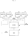
- FIG. 2 is a diagram of a structure of an electronic device having a plurality of RF chips.
- an electronic device includes one first RF chip 200 and four second RF chips 211, 212, 213, and 214.
- the first RF chip 200 and the plurality of second RF chips 211, 212, 213, and 214 are RF chips capable of performing beamforming in the mm-Wave band.
- an RF chip for implementing high frequency may be divided into the first RF chip 200 and the plurality of second RF chips 211, 212, 213, and 214.
- the plurality of second RF chips 211, 212, 213, and 214 are deployed at ends of the electronic device and radiate beams to the outside of the electronic device, they may be referred to front-end chips. Further, as described above with reference to FIG. 1 , the plurality of second RF chips 211, 212, 213, and 214 may have a plurality of RF chains.
- FIG. 2 shows an implementation capable of increasing the number of RF chains through the four second RF chips 211, 212, 213, and 214.
- the first RF chip 200 and the second RF chips 211, 212, 213, and 214 are connected to each other through different transmission lines.
- the transmission lines connecting between the first RF chip 200 and the second RF chips 211, 212, 213, and 214 may have different phases.
- the first RF chip 200 and the second RF chip 211 may be connected to each other through the transmission line having a phase of 5° ( ⁇ 1 ), and the first RF chip 200 and the second RF chip 212 may be connected to each other through the transmission line having a phase of 3° ( ⁇ 2 ). Further, the first RF chip 200 and the second RF chip 213 may be connected to each other through the transmission line having a phase of 4° ( ⁇ 3 ), and the first RF chip 200 and the second RF chip 214 may be connected to each other through the transmission line having a phase of 7° ( ⁇ 4 ).
- the respective second chips may generate beams having different phases due to the phase difference of the transmission line, and thus the beams may not be radiated at a desired angle or the gain value of the beams may be considerably reduced.
- the transmission line may refer to an RF signal line connecting between the first RF chip and the second RF chip.
- a physical cable, a PCB, and a waveguide may be included in the transmission line.
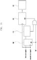
- FIG. 3 is a diagram of a structure of an electronic device having a plurality of RF chips, according to an embodiment.
- one first RF chip 200 may be connected to four second RF chips 211, 212, 213, and 214, and may be connected to a modem 400.
- the modem 400 may be a digital modem, and may modulate and demodulate signals transmitted and received through the first RF chip 200 and the second RF chip 211.
- the modem 400 may transmit a second clock signal to the first RF chip 200, and may transmit a first clock signal to the second RF chip 211. Frequencies of the first clock signal and the second clock signal should be different from each other.
- Phase measurement circuits 221, 222, 223, and 224 measuring the phase of the transmission line may be deployed on the second RF chips 211, 212, 213, and 214, respectively.
- the first RF chip 200 may transmit the second clock signal received from the modem 400 to the second RF chips 211, 212, 213, and 214, respectively.
- the phase measurement circuits 221, 222, 223, and 224 deployed on the respective second RF chips may measure phases ⁇ 1 , ⁇ 2 , ⁇ 3 , and ⁇ 4 of the transmission lines connecting between the first RF chip 200 and the second RF chips 211, 212, 213, and 214 based on the first clock signal and the second clock signal.
- FIG. 3 illustrates a case where one first RF chip 200 and four second RF chips 211, 212, 213, and 214 are deployed inside the electronic device, the scope of the present disclosure should not be limited to the number of RF chips as described above.
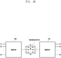
- FIG. 4A is a diagram of an internal structure of an RF chip, according to an embodiment.
- FIG. 4A a structure in which the first RF chip 200 and the second RF chip 211 are connected to each other is shown.
- the internal structure between the first RF chip and the second RF chips 212, 213, and 214 may be similar to the internal structure illustrated in FIG. 4A .
- the electronic device may include the modem 400 transmitting the first clock signal to the second RF chip 211, the first RF chip 200 connected to the modem 400 to receive the second clock signal from the modem 400, and the second RF chip 211 electrically connected to the first RF chip 200 through the transmission line to receive the second clock signal from the first RF chip 200 and to measure the phase of the transmission line based on the first clock signal and the second clock signal.
- the first RF chip 200 may control a signal that is transmitted and received through the first RF chip 200 through a black box 260. Since the detailed configuration of the black box 260 is not related to the technical feature to be described in the present disclosure, and thus may have a different structure depending on a wireless communication processor design type, explanation of the configuration of the black box 260 will be omitted in the description.
- the first RF chip 200 having received the second clock signal from the modem 400 may transmit the second clock signal to the second RF chip 211 through the transmission line.
- the first RF chip 200 and the second RF chip 211 may include frequency selectors 231 and 232, respectively, and a plurality of frequency band signals may be simultaneously transmitted and received through the transmission line.
- a frequency division transmission method through the frequency selectors 231 and 232 will be described in detail with reference to FIG. 4B .
- the second RF chip 211 may receive the second clock signal from the first RF chip 200 through the frequency selector 232, and the second clock signal may be transferred to a measurement circuit 211 deployed inside the second RF chip 211.
- a phase measurement circuit 221 may measure the phase of the transmission line based on the first clock signal received through the modem 400 and the second clock signal received through the first RF chip 200.
- the first clock signal and the second clock signal may have different frequencies. The operation of the phase measurement circuit 221 will be described in more detail with reference to FIGS. 7A , 7B , and 8 .
- the second RF chip 211 may also include a black box 270 for controlling a signal transmitted and received through the second RF chip 211 in the same manner as the first RF chip 200, and the second RF chip 211 may be connected to a plurality of antenna arrays 241 and 242 so as to radiate beams to an outside of the electronic device.
- the second RF chip 211 may further include a temperature sensor.
- the phase of the transmission line may be changed in accordance with the temperature thereof.
- the second RF chip may sense or measure a temperature change through the temperature sensor, and if the temperature change amount is greater than or equal to a predetermined temperature threshold value, the second RF chip may measure the phase of the transmission line based on the first clock signal and the second clock signal.
- the phase measurement circuit 221 may use the temperature as a trigger condition for measuring the phase of the transmission line.
- the second RF chip 211 may further include an output sensor, and the second RF chip 211 may sense and measure an output change through the output sensor, and if the output change amount is greater than or equal to a predetermined output threshold value, the second RF chip may measure the phase of the transmission line based on the first clock signal and the second clock signal.
- the second RF chip may measure the phase of the transmission line based on the first clock signal and the second clock signal.
- phase measurement circuit 221 may measure the phase of the transmission line at predetermined intervals in addition to measurement of the phase of the transmission line based on the specific trigger condition (temperature or output) as described above.
- FIG. 4B is a diagram of frequency division transmission, according to an embodiment.
- the first RF chip and the second RF chip may include the frequency selectors 231 and 232, respectively.
- the frequency selectors 231 and 232 may include duplexers or triplexers.
- frequency selectors 231 and 232 are composed of duplexers, two kinds of frequency band signals may be simultaneously transmitted and received through the transmission line (if the frequency selectors are composed of triplexers, three kinds of frequency band signals may be simultaneously transmitted and received).
- a frequency division multiple access (FDMA) communication method may be used through the frequency selectors.
- FDMA frequency division multiple access
- the electronic device may radiate beams to outside through the first RF chip and the second RF chip, and may measure the phase of the transmission line at the same time.
- a signal for forming the beams may be transmitted and received through the transmission line, and a signal for measuring the phase of the transmission line may be transmitted and received through the transmission line at the same time. Accordingly, the phase difference caused by the transmission line may be compensated for through real-time measurement of the phase of the transmission line simultaneously with the beam radiation.
- n kinds of frequency band signals may be simultaneously transmitted and received through the transmission line by the frequency selectors 231 and 232.
- FIG. 5 is a diagram of a structure of an electronic device having a plurality of RF chips, according to an embodiment.
- one first RF chip 200 may be connected to four second RF chips 211, 212, 213, and 214, and may be connected to a modem 400.
- the modem 400 may be a digital modem, and may modulate and demodulate signals transmitted and received through the first RF chip 200 and the second RF chip 211.
- Phase measurement circuits 221, 222, 223, and 224 measuring the phase of the transmission line may be deployed on the first RF chip 200.
- the first RF chip 200 may transmit the second clock signal to the respective second RF chips 211, 212, 213, and 214, and the respective second RF chips 211, 212, 213, and 214 may transmit a third clock signal obtained by converting the frequency of the second clock signal to the first RF chip 200.
- Respective phase measurement circuits 221, 222, 223, and 224 may measure phases ⁇ 1 , ⁇ 2 , ⁇ 3 , and ⁇ 4 of the transmission lines connecting between the first RF chip 200 and the respective second RF chips 211, 212, 213, and 214 based on the third clock signal and the first clock signal received from the modem 400.
- FIG. 5 illustrates a case where one first RF chip 200 and four second RF chips 211, 212, 213, and 214 are deployed inside the electronic device, the scope of the disclosure should not be limited to the number of RF chips as described above.
- FIG. 6 is a diagram of an internal structure of an RF chip, according to an embodiment.
- the phase measurement circuit 221 for measuring the phase of the transmission line connecting between the first RF chip 200 and the second RF chip 211 are deployed within the first RF chip 200.
- the first RF chip 200 having received the second clock signal from the modem 400 to measure the phase of the transmission line transmits this to the second RF chip 211, and the second RF chip 211 converts the second clock signal into the third clock signal through a frequency converter 250.
- the third clock signal converted through the frequency converter 250 is transferred to the phase measurement circuit 221 of the first RF chip 200, and the phase measurement circuit 221 may measure the phase of the transmission line based on the first clock signal and the third clock signal received from the modem 400.
- the clock signal reciprocates between the first RF chip 200 and the second RF chip 211 through the transmission line.
- the respective RF chips include the frequency selectors 231 and 232, and the second clock signal and the third clock signal can be simultaneously transmitted and received through the transmission line.
- the frequency selectors 231 and 232 are composed of triplexers capable of simultaneously transmitting and receiving three or more frequency band signals, not only the signal for the beam radiation but also the second clock signal and the third clock signal for the transmission line measurement can be simultaneously transmitted and received through the transmission line as described above, and thus it becomes possible to perform real-time phase measurement of the transmission line.
- the frequency converter 250 of the second RF chip 211 may generate the third clock signal through conversion of the frequency of the second clock signal into another frequency.
- the frequency converter 250 may convert the frequency of the second clock signal into the frequency of the third clock signal so that the frequency of the third clock signal becomes lower than the frequency of the second clock signal. Accordingly, it is possible to simultaneously send and receive a plurality of signals in a frequency division method through one transmission line.
- the frequency of the third clock signal may be 200 MHz, and the phase measurement circuit 221 may measure the phase of the transmission line connecting between the first RF chip and the second RF chip based on the frequency of the third clock signal and the frequency f 1 of the first clock signal having 200.1 MHz.
- FIGS. 7A and 7B are diagrams of a configuration of a phase measurement circuit, according to an embodiment.
- phase measurement circuit illustrated in FIGS. 7A and 7B is a phase measurement circuit operating based on the first clock signal and the second clock signal, it may correspond a phase measurement circuit in the electronic device structure as illustrated in FIGS. 3 and 4A .
- the phase measurement circuit may include a flip-flop 700 receiving an input of the first clock signal and the second clock signal.
- the flip-flop is a circuit that is called a trigger circuit, and can preserve either of two stable states. If an initial state is "1", the flip-flop continuously maintains the state of "1” so far as there is no input of an opposite state, whereas it is changed to a state of "0" if there is an input of an opposite signal.
- Various types of flip-flops such as R-S flip-flop, J-K flip-flop, D flip-flop, and T flip-flop, may be configured.
- a reset trigger (RST) flip-flop is illustrated as a flip-flop.
- the RST flip-flop is a kind of RS flip-flop in which an input terminal that is in synchronization with a clock pulse is deployed, and its output may be changed based on a predetermined truth table.
- the phase measurement circuit may further include a negative edge detector 710, a counter 720, and a memory 730, in addition to the flip-flop.
- the phase measurement circuit may record in the memory 730 a time in which the phase difference between the first clock signal and the second clock signal becomes a half period through the negative edge detector 710 and the counter 720. Through this, high-resolution time measurement may become possible.
- the phase measurement circuit illustrated in FIG. 7A is a circuit for converting the phase difference of the transmission line into a digital value with the resolution as much as the period difference between the first clock signal and the second clock signal, and a method for measuring the phase of the transmission line through the circuit will be described with reference to FIG. 8 .
- FIG. 7B is a diagram of a phase measurement circuit including a phase detector receiving an input of the first clock signal and the second clock signal.
- the phase detector may measure the phase difference between two input frequencies through comparison, and may output a clock signal corresponding to the difference.
- phase measurement circuit of FIG. 7B is similar to the operation of the phase measurement circuit of FIG. 7A , and thus the detailed explanation of the phase measurement circuit illustrated in FIG. 7B is replaced by the explanation with reference to FIGS. 7A and 8 .
- a third clock signal and a fourth clock signal may be additionally considered.
- the first to fourth clock signals should have different frequencies from each other, and the phase measurement circuit may measure the phase of the transmission line based on the third clock signal and the fourth clock signal.
- the number of times of phase measurement of the transmission line becomes greater than that when using the two clock signals, and thus the resolution of the phase measurement of the transmission line may be improved.
- time and a load may become greater in measuring the phase of the transmission line, it is required to design the phase measurement circuit in consideration of the two merits and demerits as described above.
- phase measurement circuit as illustrated in FIGS. 7A and 7B can be implemented using other logic circuits capable of performing the same operation, the scope of the present disclosure should not be limited to only the circuit structure illustrated in FIGS. 7A and 7B .
- FIG. 8 is a diagram of measuring a phase of a transmission line through a phase measurement circuit, according to an embodiment.
- the first clock signal input through the flip-flop may have the frequency f 1
- the second clock signal may have the frequency f 2 .
- a half period of the first clock signal may be 1/(2f 1 )
- a half period of the second clock signal may be 1/(2f 2 ).
- the second clock signal may maintain the original state in a moment that the first clock signal is changed from “1" to "0", and in this instance, the output of the flip-flop may continuously maintain the value of "1".
- the counter circuit may perform counting for measuring the phase of the transmission line with the resolution as much as the period difference between the first clock signal and the second clock signal, and at a time when the output of the flip-flop is changed from "1" to "0", the counter circuit may store the counted value in the memory, and measure the phase of the transmission line using the counted value.
- the period difference between the first clock signal and the second clock signal becomes 2.12 ps.
- phase measurement circuit should be reset, and thereafter, in the same manner as described above, the phase of the transmission line may be measured based on the value counted by the counter circuit at a time when the output of the flip-flop is changed from "1" to "0".
- the minimum unit in which the phase of the transmission line is measured may be determined by the half-period difference between the first clock signal and the second clock signal, and high-resolution phase measurement may become possible even if the first clock signal and the second clock signal having low frequencies are used.
- FIG. 9 is a diagram of measuring a phase of a transmission line connecting between a first RF chip and a second RF chip, according to an embodiment.
- the second RF chip may receive the first clock signal from the modem. Further, at step S920, the second RF chip may receive the second clock signal transmitted from the modem through the first RF chip, and, at step S930, the second RF chip may input the first clock signal and the second clock signal to the phase detector.
- phase detector may be changed to another type of circuit (flip-flop circuit).
- the phase of the transmission line may be measured based on the output value of the phase detector and the frequency difference between the first clock signal and the second clock signal.
- the method for measuring the phase of the transmission line through step S940 is described with reference to FIG. 8 .
- FIGS. 10A and 10B are diagrams of measuring a phase, according to an embodiment not covered by the claims.
- FIG. 10A illustrates a method for measuring the phase of the transmission line based on the temperature change of the RF chips
- FIG. 10B illustrates a method for measuring the phase of the transmission line based on the output change of the RF chips.
- the temperature change of the second RF chip may be sensed. More specifically, as described above, the second RF chip itself may include a temperature change sensing sensor, and using the sensor, the temperature change can be sensed.
- the second RF chip may determine whether the sensed temperature change is greater than or equal to the temperature threshold value. More specifically, if the sensed temperature change is 30°C, and the temperature threshold value is 20°C, it may be determined that the sensed temperature change through step S1020 is greater than or equal to the temperature threshold value.
- the second RF chip does not measure the phase of the transmission line.
- the second RF chip may measure the phase of the transmission line at step S1030.
- the output change of the second RF chip may be sensed. More specifically, as described above, the second RF chip itself may include an output change sensing sensor, and using the sensor, the output change can be sensed.
- the second RF chip may determine whether the sensed output change is greater than or equal to the output threshold value, and if the output change is less than the output threshold value at step S1050, there is a low possibility that there is a big difference between the current phase of the transmission line and the previously measured phase of the transmission line, and the second RF chip does not measure the phase of the transmission line.
- FIGS. 10A and 10B illustrate only the method for measuring the phase of the transmission line based on the temperature change and the output change of the second RF chip, it is also possible to determine whether to measure the phase of the transmission line based on the temperature change and the output change of the first RF chip in case where the phase measurement circuit is included in the first RF chip. Accordingly, the scope of the present disclosure should not be limited to only the technical feature illustrated in FIGS. 10A and 10B .
- the present disclosure provides a method capable of accurately measuring the phase of beams created through a plurality of RF chips in a system structure using the respective RF chips. More specifically, the present disclosure provides a method capable of accurately measuring the phase of a transmission line connecting between a first RF chip and a second RF chip in case where a wireless communication system is composed of the first and second RF chips.
- the number of times of phase measurement of the transmission line connecting a plurality of RF chips at low power can be improved, and through this, the phase of the transmission line can be accurately measured.
- accuracy of the phase measurement can be improved through performing of the phase measurement with two or more frequencies.
- phase compensation of the transmission line based on this becomes possible, and thus real-time transmission-line phase measurement and the phase compensation based on this become possible even while beams are radiated to the outside of an electronic device through the RF chips.
- the invention may be implemented by software including an instruction stored in a machine-readable storage media readable by a machine (e.g., a computer).
- the machine may be a device that calls the instruction from the machine-readable storage media and operates depending on the called instruction and may include the electronic device.
- the processor may perform a function corresponding to the instruction directly or using other components under the control of the processor.
- the instruction may include a code generated or executed by a compiler or an interpreter.
- the machine-readable storage media may be provided in the form of non-transitory storage media.
- non-transitory is a limitation of the medium itself (i.e., tangible, not a signal) as opposed to a limitation on data storage persistency.
- the method according to various embodiments disclosed in the present disclosure may be provided as a part of a computer program product.
- the computer program product may be traded between a seller and a buyer as a product.
- the computer program product may be distributed in the form of machine-readable storage medium (e.g., a compact disc read only memory (CD-ROM)) or may be distributed only through an application store (e.g., a Play Store TM ).
- an application store e.g., a Play Store TM
- at least a portion of the computer program product may be temporarily stored or generated in a storage medium such as a memory of a manufacturer's server, an application store's server, or a relay server.
- Each component may include at least one of the above components, and a portion of the above sub-components may be omitted, or additional other sub-components may be further included.
- some components may be integrated in one component and may perform the same or similar functions performed by each corresponding components prior to the integration. Operations performed by a module, a programming, or other components according to various embodiments of the present disclosure may be executed sequentially, in parallel, repeatedly, or in a heuristic method. Also, at least some operations may be executed in different sequences, omitted, or other operations may be added.
Landscapes
- Engineering & Computer Science (AREA)
- Signal Processing (AREA)
- Computer Networks & Wireless Communication (AREA)
- Physics & Mathematics (AREA)
- Electromagnetism (AREA)
- Transceivers (AREA)
- Mobile Radio Communication Systems (AREA)
- Arrangements For Transmission Of Measured Signals (AREA)
- Measuring Phase Differences (AREA)
Claims (15)
- Elektronische Vorrichtung, aufweisend einen ersten Hochfrequenzchip, radio frequency - RF, RF-Chip, (200) und einen zweiten RF-Chip (211, 212, 213, 214), umfassend:ein Modem (400), das für Folgendes konfiguriert ist:Übertragen eines ersten Taktsignals an den zweiten RF-Chip (211, 212, 213, 214) undÜbertragen eines zweiten Taktsignals an den ersten RF-Chip (200), wobei das zweite Taktsignal eine andere Frequenz als das erste Taktsignal aufweist;wobei der erste RF-Chip (200) mit dem Modem (400) verbunden und dazu konfiguriert ist, das zweite Taktsignal von dem Modem (400) zu empfangen; undder zweite RF-Chip (211, 212, 213, 214) über eine Übertragungsleitung elektrisch mit dem ersten RF-Chip (200) verbunden und für Folgendes konfiguriert ist:
Empfangen des zweiten Taktsignals von dem ersten RF-Chip (200) und Messen einer Phase der Übertragungsleitung zwischen dem ersten RF-Chip (200) und dem zweiten RF-Chip (211, 212, 213, 214) auf der Grundlage des ersten Taktsignals und des zweiten Taktsignals, um eine durch die Übertragungsleitung verursachte Phasendifferenz zu kompensieren. - Elektronische Vorrichtung nach Anspruch 1, wobei der zweite RF-Chip (211, 212, 213, 214) einen Phasendetektor umfasst, der dazu konfiguriert ist, eine Eingabe des ersten Taktsignals und des zweiten Taktsignals zu empfangen, und
wobei der zweite RF-Chip (211, 212, 213, 214) dazu konfiguriert ist, die Phase der Übertragungsleitung auf der Grundlage einer Ausgabeänderung des Phasendetektors zu messen. - Elektronische Vorrichtung nach Anspruch 1, wobei der zweite RF-Chip (211, 212, 213, 214) ein Flipflop umfasst, das dazu konfiguriert ist, eine Eingabe des ersten Taktsignals und des zweiten Taktsignals zu empfangen,wobei der zweite RF-Chip (211, 212, 213, 214) dazu konfiguriert ist, die Phase der Übertragungsleitung auf der Grundlage einer Ausgabeänderung des Flipflops zu messen,wobei der zweite RF-Chip (211, 212, 213, 214) ferner einen Zähler umfasst, der dazu konfiguriert ist, die Eingabe des ersten Taktsignals und des zweiten Taktsignals zu empfangen, undwobei der zweite RF-Chip (211, 212, 213, 214) dazu konfiguriert ist, die Phase der Übertragungsleitung auf der Grundlage eines Ausgabewertes des Zählers und einer Frequenzdifferenz zwischen dem ersten Taktsignal und dem zweiten Taktsignal zu messen, falls ein Ausgabewert des Flipflops geändert wird.
- Elektronische Vorrichtung nach Anspruch 1, wobei der erste RF-Chip (200) und der zweite RF-Chip (211, 212, 213, 214) einen Frequenzselektor umfassen, der dazu konfiguriert ist zu ermöglichen, dass eine Mehrzahl von Frequenzbandsignalen über die Übertragungsleitung übertragen und empfangen wird.
- Elektronische Vorrichtung nach Anspruch 1, wobei das Modem (400) dazu konfiguriert ist, ein drittes Taktsignal an den zweiten RF-Chip (211, 212, 213, 214) zu übertragen,der erste RF-Chip (200) dazu konfiguriert ist, ein viertes Taktsignal von dem Modem (400) zu empfangen,der zweite RF-Chip (211, 212, 213, 214) dazu konfiguriert ist, das vierte Taktsignal von dem ersten RF-Chip (200) zu empfangen, und dazu konfiguriert ist, die Phase der Übertragungsleitung auf der Grundlage des dritten Taktsignals und des vierten Taktsignals zu messen, unddas erste bis vierte Taktsignal Frequenzen aufweisen, die sich voneinander unterscheiden.
- Elektronische Vorrichtung nach Anspruch 1, wobei der zweite RF-Chip (211, 212, 213, 214) einen Temperatursensor umfasst, der dazu konfiguriert ist, eine Temperatur des zweiten RF-Chips (211, 212, 213, 214) zu erfassen, und
wobei der zweite RF-Chip (211, 212, 213, 214) dazu konfiguriert ist, die Phase der Übertragungsleitung auf der Grundlage des ersten Taktsignals und des zweiten Taktsignals zu messen, falls eine durch den Temperatursensor erfasste Temperaturänderung des zweiten RF-Chips (211, 212, 213, 214) größer als ein oder gleich einem vorgegebener/n Temperaturschwellenwert ist. - Elektronische Vorrichtung nach Anspruch 1, wobei der zweite RF-Chip (211, 212, 213, 214) einen Ausgabesensor umfasst, der dazu konfiguriert ist, eine Ausgabe des zweiten RF-Chips (211, 212, 213, 214) zu erfassen, und
wobei der zweite RF-Chip (211, 212, 213, 214) dazu konfiguriert ist, die Phase der Übertragungsleitung auf der Grundlage des ersten Taktsignals und des zweiten Taktsignals zu messen, falls eine durch den Ausgabesensor erfasste Ausgabeänderung des zweiten RF-Chips (211, 212, 213, 214) größer als ein oder gleich einem vorgegebener/n Ausgabeschwellenwert ist. - Elektronische Vorrichtung, aufweisend einen ersten Hochfrequenzchip, radio frequency - RF, RF-Chip, und einen zweiten RF-Chip (211, 212, 213, 214), umfassend:ein Modem (400), das dazu konfiguriert ist, ein erstes Taktsignal und ein zweites Taktsignal an den ersten RF-Chip (200) zu übertragen, wobei das erste Taktsignal und das zweite Taktsignal Frequenzen aufweisen, die sich voneinander unterscheiden;wobei der erste RF-Chip (200) über eine Übertragungsleitung elektrisch mit dem zweiten RF-Chip (211, 212, 213, 214) verbunden und für Folgendes konfiguriert ist:Übertragen des zweiten Taktsignals an den zweiten RF-Chip (211, 212, 213, 214),Empfangen, von dem zweiten RF-Chip (211, 212, 213, 214), eines dritten Taktsignals, rückgekoppelt entsprechend dem zweiten Taktsignal, undMessen einer Phase der Übertragungsleitung zwischen dem ersten RF-Chip (200) und dem zweiten RF-Chip (211, 212, 213, 214) auf der Grundlage des ersten Taktsignals und des dritten Taktsignals, um eine durch die Übertragungsleitung verursachte Phasendifferenz zu kompensieren; undwobei der zweite RF-Chip (211, 212, 213, 214) dazu ausgebildet ist, Strahlen in die Umgebung der elektronischen Vorrichtung abzustrahlen.
- Elektronische Vorrichtung nach Anspruch 8, wobei der erste RF-Chip (200) einen Phasendetektor umfasst, der dazu konfiguriert ist, eine Eingabe des ersten Taktsignals und des dritten Taktsignals zu empfangen, und
wobei der erste RF-Chip (200) dazu konfiguriert ist, die Phase der Übertragungsleitung auf der Grundlage einer Ausgabeänderung des Phasendetektors zu messen. - Elektronische Vorrichtung nach Anspruch 8, wobei der erste RF-Chip (200) ein Flipflop umfasst, das dazu konfiguriert ist, eine Eingabe des ersten Taktsignals und des dritten Taktsignals zu empfangen,wobei der erste RF-Chip (200) dazu konfiguriert ist, die Phase der Übertragungsleitung auf der Grundlage einer Ausgabeänderung des Flipflops zu messen,wobei der erste RF-Chip (200) ferner einen Zähler umfasst, der dazu konfiguriert ist, die Eingabe des ersten Taktsignals und des dritten Taktsignals zu empfangen, undwobei der erste RF-Chip (200) dazu konfiguriert ist, die Phase der Übertragungsleitung auf der Grundlage eines Ausgabewertes des Zählers und einer Frequenzdifferenz zwischen dem ersten Taktsignal und dem dritten Taktsignal zu messen, falls ein Ausgabewert des Flipflops geändert wird.
- Elektronische Vorrichtung nach Anspruch 8, wobei der erste RF-Chip (200) und der zweite RF-Chip (211, 212, 213, 214) einen Frequenzselektor umfassen, der dazu konfiguriert ist zu ermöglichen, dass eine Mehrzahl von Frequenzbandsignalen über die Übertragungsleitung übertragen und empfangen wird.
- Elektronische Vorrichtung nach Anspruch 8, wobei der zweite RF-Chip (211, 212, 213, 214) einen Frequenzumsetzer umfasst und
wobei durch den Frequenzumsetzer die Frequenz des ersten Taktsignals in die Frequenz des zweiten Taktsignals umgesetzt wird. - Elektronische Vorrichtung nach Anspruch 12, wobei die Frequenz des ersten Taktsignals höher als die Frequenz des zweiten Taktsignals ist.
- Elektronische Vorrichtung nach Anspruch 8, wobei der erste RF-Chip (200) einen Temperatursensor umfasst, der dazu konfiguriert ist, eine Temperatur des ersten RF-Chips (200) zu erfassen, und
wobei der erste RF-Chip (200) dazu konfiguriert ist, die Phase der Übertragungsleitung auf der Grundlage des ersten Taktsignals und des dritten Taktsignals zu messen, falls eine durch den Temperatursensor erfasste Temperaturänderung des ersten RF-Chips (200) größer als ein oder gleich einem vorgegebener/n Temperaturschwellenwert ist. - Elektronische Vorrichtung nach Anspruch 8, wobei der erste RF-Chip (200) einen Ausgabesensor umfasst, der dazu konfiguriert ist, eine Ausgabe des ersten RF-Chips (200) zu erfassen, und
wobei der erste RF-Chip (200) dazu konfiguriert ist, die Phase der Übertragungsleitung auf der Grundlage des ersten Taktsignals und des dritten Taktsignals zu messen, falls eine durch den Ausgabesensor erfasste Ausgabeänderung des ersten RF-Chips (200) größer als ein oder gleich einem vorgegebener/n Ausgabeschwellenwert ist.
Applications Claiming Priority (1)
| Application Number | Priority Date | Filing Date | Title |
|---|---|---|---|
| KR1020170147853A KR102376725B1 (ko) | 2017-11-08 | 2017-11-08 | Rf 칩을 연결하는 전송선로의 위상 측정 방법 및 이를 위한 장치 |
Publications (2)
| Publication Number | Publication Date |
|---|---|
| EP3484087A1 EP3484087A1 (de) | 2019-05-15 |
| EP3484087B1 true EP3484087B1 (de) | 2021-12-01 |
Family
ID=64048798
Family Applications (1)
| Application Number | Title | Priority Date | Filing Date |
|---|---|---|---|
| EP18203446.2A Active EP3484087B1 (de) | 2017-11-08 | 2018-10-30 | Vorrichtung zur messung der phase einer übertragungsleitung, die zwischen hochfrequenzchips geschaltet ist |
Country Status (4)
| Country | Link |
|---|---|
| US (1) | US11171415B2 (de) |
| EP (1) | EP3484087B1 (de) |
| KR (1) | KR102376725B1 (de) |
| CN (1) | CN109756281B (de) |
Families Citing this family (4)
| Publication number | Priority date | Publication date | Assignee | Title |
|---|---|---|---|---|
| CN110417442B (zh) * | 2019-06-21 | 2021-12-10 | 成都天锐星通科技有限公司 | 一种集成波束控制算法的射频芯片及芯片处理方法 |
| WO2021025545A1 (ko) * | 2019-08-08 | 2021-02-11 | 포항공과대학교 산학협력단 | Rf 체인의 특성을 측정하기 위한 방법 및 장치 |
| EP3936882A1 (de) * | 2020-07-07 | 2022-01-12 | Koninklijke Philips N.V. | Magnetresonanzbildgebungssystem und verfahren mit frequenzkalibrierung mittels eines signals eines geosatelliten-positionierungssystems |
| WO2023043295A1 (ko) * | 2021-09-17 | 2023-03-23 | 주식회사 포인투테크놀로지 | Pi-기반 코스타스 루프를 이용한 캐리어 동기화를 갖는 50 gb/s pam4 양-방향 플라스틱 웨이브가이드 링크 |
Family Cites Families (15)
| Publication number | Priority date | Publication date | Assignee | Title |
|---|---|---|---|---|
| FR2682841B1 (fr) * | 1991-10-21 | 1993-11-19 | Alcatel Telspace | Procede de detection de faux accrochages d'un signal de reference sur un signal initialement module en modulation numerique plurivalente decalee, procede de demodulation numerique coherente l'utilisant. |
| US6717478B1 (en) * | 2001-04-09 | 2004-04-06 | Silicon Image | Multi-phase voltage controlled oscillator (VCO) with common mode control |
| US6865135B2 (en) * | 2003-03-12 | 2005-03-08 | Micron Technology, Inc. | Multi-frequency synchronizing clock signal generator |
| JP3841077B2 (ja) * | 2003-10-17 | 2006-11-01 | ソニー株式会社 | デジタル変調回路およびデジタル変調方法、デジタル復調回路およびデジタル復調方法、復調用キャリアの生成回路および生成方法、並びに復調用ビットクロックの生成回路および生成方法 |
| KR100990484B1 (ko) * | 2004-03-29 | 2010-10-29 | 삼성전자주식회사 | 직렬 버스 통신을 위한 송신 클럭 신호 발생기 |
| US8102665B2 (en) * | 2006-06-21 | 2012-01-24 | Broadcom Corporation | Integrated circuit with intra-chip clock interface and methods for use therewith |
| US8756557B2 (en) * | 2007-05-09 | 2014-06-17 | Synopsys, Inc. | Techniques for use with automated circuit design and simulations |
| US7733975B1 (en) * | 2008-12-31 | 2010-06-08 | Mediatek Inc. | Method for estimating phase error in MIMO OFDM communications system |
| US9621330B2 (en) | 2011-11-30 | 2017-04-11 | Maxlinear Asia Singapore Private Limited | Split microwave backhaul transceiver architecture with coaxial interconnect |
| US8693601B2 (en) * | 2012-01-03 | 2014-04-08 | Intel Corporation | Self-correcting multirate filter |
| KR102076326B1 (ko) * | 2013-05-09 | 2020-02-12 | 삼성전자주식회사 | 위상 로테이팅 위상동기회로 및 그것의 동작 제어방법 |
| EP2871494B1 (de) * | 2013-11-08 | 2018-03-21 | u-blox AG | Phasenausrichtung zwischen Taktsignalen |
| JP2015233192A (ja) * | 2014-06-09 | 2015-12-24 | 富士通株式会社 | 無線装置、及び、無線装置の制御方法 |
| KR102595903B1 (ko) * | 2016-08-26 | 2023-10-30 | 삼성전자주식회사 | 모뎀 칩, 이를 포함하는 어플리케이션 프로세서 및 모뎀 칩의 동작방법 |
| US11153067B2 (en) * | 2019-05-14 | 2021-10-19 | Space Exploration Technologies Corp. | Chip to chip time synchronization |
-
2017
- 2017-11-08 KR KR1020170147853A patent/KR102376725B1/ko active Active
-
2018
- 2018-10-30 EP EP18203446.2A patent/EP3484087B1/de active Active
- 2018-10-31 CN CN201811283791.8A patent/CN109756281B/zh not_active Expired - Fee Related
- 2018-11-01 US US16/177,767 patent/US11171415B2/en active Active
Also Published As
| Publication number | Publication date |
|---|---|
| CN109756281A (zh) | 2019-05-14 |
| EP3484087A1 (de) | 2019-05-15 |
| US11171415B2 (en) | 2021-11-09 |
| US20190140721A1 (en) | 2019-05-09 |
| KR20190052294A (ko) | 2019-05-16 |
| KR102376725B1 (ko) | 2022-03-21 |
| CN109756281B (zh) | 2022-11-04 |
Similar Documents
| Publication | Publication Date | Title |
|---|---|---|
| US11114771B2 (en) | Antenna device and electronic device including the same | |
| US11218902B2 (en) | Method and apparatus for configuring QoS flow in wireless communication system | |
| EP3484087B1 (de) | Vorrichtung zur messung der phase einer übertragungsleitung, die zwischen hochfrequenzchips geschaltet ist | |
| US10560958B2 (en) | Interface device and method in wireless communication network | |
| KR102272844B1 (ko) | 타이밍 어드밴스 제어 방법 및 장치 | |
| US10841052B2 (en) | Multi-numerology based data transmitting and receiving method and apparatus capable of frequency hopping in OFDM system | |
| WO2023230951A1 (en) | Techniques for baseband frequency shifting | |
| CN111492613B (zh) | 用于在无线蜂窝通信系统中配置解调参考信号信息的方法和装置 | |
| WO2023240429A1 (en) | Radio frequency energy harvesting configuration | |
| US20190327120A1 (en) | Device and method for reducing peak-to-average power ratio in wireless communication system | |
| KR102388027B1 (ko) | 무선통신 모듈의 시험 방법 및 상기 무선통신 모듈을 포함하는 전자 장치 | |
| US12184357B2 (en) | Methods for selection of antenna arrays and beamforming feedback | |
| US12531693B2 (en) | Sounding reference signal port enhancements for uplink transmissions | |
| CN120457643A (zh) | 无线通信系统中确定ris关联的方法和装置 | |
| US12136971B2 (en) | Methods for communicating training data to a machine learning server for blockage modeling and blockage mitigation | |
| WO2024254821A1 (en) | Methods for handling backscatter link failure | |
| WO2025081295A1 (en) | Frequency shifting techniques for backscatter communications | |
| WO2025076846A1 (en) | Techniques for beam management | |
| WO2025050233A1 (en) | Ambient internet-of-things tag information indication |
Legal Events
| Date | Code | Title | Description |
|---|---|---|---|
| PUAI | Public reference made under article 153(3) epc to a published international application that has entered the european phase |
Free format text: ORIGINAL CODE: 0009012 |
|
| STAA | Information on the status of an ep patent application or granted ep patent |
Free format text: STATUS: THE APPLICATION HAS BEEN PUBLISHED |
|
| AK | Designated contracting states |
Kind code of ref document: A1 Designated state(s): AL AT BE BG CH CY CZ DE DK EE ES FI FR GB GR HR HU IE IS IT LI LT LU LV MC MK MT NL NO PL PT RO RS SE SI SK SM TR |
|
| AX | Request for extension of the european patent |
Extension state: BA ME |
|
| STAA | Information on the status of an ep patent application or granted ep patent |
Free format text: STATUS: REQUEST FOR EXAMINATION WAS MADE |
|
| 17P | Request for examination filed |
Effective date: 20190821 |
|
| RBV | Designated contracting states (corrected) |
Designated state(s): AL AT BE BG CH CY CZ DE DK EE ES FI FR GB GR HR HU IE IS IT LI LT LU LV MC MK MT NL NO PL PT RO RS SE SI SK SM TR |
|
| RIC1 | Information provided on ipc code assigned before grant |
Ipc: H04L 5/00 20060101AFI20210506BHEP Ipc: H04B 7/00 20060101ALI20210506BHEP Ipc: H04B 17/14 20150101ALI20210506BHEP Ipc: H04L 7/00 20060101ALI20210506BHEP |
|
| GRAP | Despatch of communication of intention to grant a patent |
Free format text: ORIGINAL CODE: EPIDOSNIGR1 |
|
| STAA | Information on the status of an ep patent application or granted ep patent |
Free format text: STATUS: GRANT OF PATENT IS INTENDED |
|
| INTG | Intention to grant announced |
Effective date: 20210624 |
|
| RIN1 | Information on inventor provided before grant (corrected) |
Inventor name: LEE, JEONGHO Inventor name: LEE, DAEYOUNG Inventor name: YANG, SUNGGI |
|
| GRAS | Grant fee paid |
Free format text: ORIGINAL CODE: EPIDOSNIGR3 |
|
| GRAA | (expected) grant |
Free format text: ORIGINAL CODE: 0009210 |
|
| STAA | Information on the status of an ep patent application or granted ep patent |
Free format text: STATUS: THE PATENT HAS BEEN GRANTED |
|
| AK | Designated contracting states |
Kind code of ref document: B1 Designated state(s): AL AT BE BG CH CY CZ DE DK EE ES FI FR GB GR HR HU IE IS IT LI LT LU LV MC MK MT NL NO PL PT RO RS SE SI SK SM TR |
|
| REG | Reference to a national code |
Ref country code: GB Ref legal event code: FG4D |
|
| REG | Reference to a national code |
Ref country code: AT Ref legal event code: REF Ref document number: 1452807 Country of ref document: AT Kind code of ref document: T Effective date: 20211215 Ref country code: CH Ref legal event code: EP |
|
| REG | Reference to a national code |
Ref country code: IE Ref legal event code: FG4D |
|
| REG | Reference to a national code |
Ref country code: DE Ref legal event code: R096 Ref document number: 602018027427 Country of ref document: DE |
|
| REG | Reference to a national code |
Ref country code: LT Ref legal event code: MG9D |
|
| REG | Reference to a national code |
Ref country code: NL Ref legal event code: MP Effective date: 20211201 |
|
| REG | Reference to a national code |
Ref country code: AT Ref legal event code: MK05 Ref document number: 1452807 Country of ref document: AT Kind code of ref document: T Effective date: 20211201 |
|
| PG25 | Lapsed in a contracting state [announced via postgrant information from national office to epo] |
Ref country code: RS Free format text: LAPSE BECAUSE OF FAILURE TO SUBMIT A TRANSLATION OF THE DESCRIPTION OR TO PAY THE FEE WITHIN THE PRESCRIBED TIME-LIMIT Effective date: 20211201 Ref country code: LT Free format text: LAPSE BECAUSE OF FAILURE TO SUBMIT A TRANSLATION OF THE DESCRIPTION OR TO PAY THE FEE WITHIN THE PRESCRIBED TIME-LIMIT Effective date: 20211201 Ref country code: FI Free format text: LAPSE BECAUSE OF FAILURE TO SUBMIT A TRANSLATION OF THE DESCRIPTION OR TO PAY THE FEE WITHIN THE PRESCRIBED TIME-LIMIT Effective date: 20211201 Ref country code: BG Free format text: LAPSE BECAUSE OF FAILURE TO SUBMIT A TRANSLATION OF THE DESCRIPTION OR TO PAY THE FEE WITHIN THE PRESCRIBED TIME-LIMIT Effective date: 20220301 Ref country code: AT Free format text: LAPSE BECAUSE OF FAILURE TO SUBMIT A TRANSLATION OF THE DESCRIPTION OR TO PAY THE FEE WITHIN THE PRESCRIBED TIME-LIMIT Effective date: 20211201 |
|
| PG25 | Lapsed in a contracting state [announced via postgrant information from national office to epo] |
Ref country code: SE Free format text: LAPSE BECAUSE OF FAILURE TO SUBMIT A TRANSLATION OF THE DESCRIPTION OR TO PAY THE FEE WITHIN THE PRESCRIBED TIME-LIMIT Effective date: 20211201 Ref country code: PL Free format text: LAPSE BECAUSE OF FAILURE TO SUBMIT A TRANSLATION OF THE DESCRIPTION OR TO PAY THE FEE WITHIN THE PRESCRIBED TIME-LIMIT Effective date: 20211201 Ref country code: NO Free format text: LAPSE BECAUSE OF FAILURE TO SUBMIT A TRANSLATION OF THE DESCRIPTION OR TO PAY THE FEE WITHIN THE PRESCRIBED TIME-LIMIT Effective date: 20220301 Ref country code: LV Free format text: LAPSE BECAUSE OF FAILURE TO SUBMIT A TRANSLATION OF THE DESCRIPTION OR TO PAY THE FEE WITHIN THE PRESCRIBED TIME-LIMIT Effective date: 20211201 Ref country code: HR Free format text: LAPSE BECAUSE OF FAILURE TO SUBMIT A TRANSLATION OF THE DESCRIPTION OR TO PAY THE FEE WITHIN THE PRESCRIBED TIME-LIMIT Effective date: 20211201 Ref country code: GR Free format text: LAPSE BECAUSE OF FAILURE TO SUBMIT A TRANSLATION OF THE DESCRIPTION OR TO PAY THE FEE WITHIN THE PRESCRIBED TIME-LIMIT Effective date: 20220302 Ref country code: ES Free format text: LAPSE BECAUSE OF FAILURE TO SUBMIT A TRANSLATION OF THE DESCRIPTION OR TO PAY THE FEE WITHIN THE PRESCRIBED TIME-LIMIT Effective date: 20211201 |
|
| PG25 | Lapsed in a contracting state [announced via postgrant information from national office to epo] |
Ref country code: NL Free format text: LAPSE BECAUSE OF FAILURE TO SUBMIT A TRANSLATION OF THE DESCRIPTION OR TO PAY THE FEE WITHIN THE PRESCRIBED TIME-LIMIT Effective date: 20211201 |
|
| PG25 | Lapsed in a contracting state [announced via postgrant information from national office to epo] |
Ref country code: SM Free format text: LAPSE BECAUSE OF FAILURE TO SUBMIT A TRANSLATION OF THE DESCRIPTION OR TO PAY THE FEE WITHIN THE PRESCRIBED TIME-LIMIT Effective date: 20211201 Ref country code: SK Free format text: LAPSE BECAUSE OF FAILURE TO SUBMIT A TRANSLATION OF THE DESCRIPTION OR TO PAY THE FEE WITHIN THE PRESCRIBED TIME-LIMIT Effective date: 20211201 Ref country code: RO Free format text: LAPSE BECAUSE OF FAILURE TO SUBMIT A TRANSLATION OF THE DESCRIPTION OR TO PAY THE FEE WITHIN THE PRESCRIBED TIME-LIMIT Effective date: 20211201 Ref country code: PT Free format text: LAPSE BECAUSE OF FAILURE TO SUBMIT A TRANSLATION OF THE DESCRIPTION OR TO PAY THE FEE WITHIN THE PRESCRIBED TIME-LIMIT Effective date: 20220401 Ref country code: EE Free format text: LAPSE BECAUSE OF FAILURE TO SUBMIT A TRANSLATION OF THE DESCRIPTION OR TO PAY THE FEE WITHIN THE PRESCRIBED TIME-LIMIT Effective date: 20211201 Ref country code: CZ Free format text: LAPSE BECAUSE OF FAILURE TO SUBMIT A TRANSLATION OF THE DESCRIPTION OR TO PAY THE FEE WITHIN THE PRESCRIBED TIME-LIMIT Effective date: 20211201 |
|
| REG | Reference to a national code |
Ref country code: DE Ref legal event code: R097 Ref document number: 602018027427 Country of ref document: DE |
|
| PG25 | Lapsed in a contracting state [announced via postgrant information from national office to epo] |
Ref country code: IS Free format text: LAPSE BECAUSE OF FAILURE TO SUBMIT A TRANSLATION OF THE DESCRIPTION OR TO PAY THE FEE WITHIN THE PRESCRIBED TIME-LIMIT Effective date: 20220401 |
|
| PLBE | No opposition filed within time limit |
Free format text: ORIGINAL CODE: 0009261 |
|
| STAA | Information on the status of an ep patent application or granted ep patent |
Free format text: STATUS: NO OPPOSITION FILED WITHIN TIME LIMIT |
|
| PG25 | Lapsed in a contracting state [announced via postgrant information from national office to epo] |
Ref country code: DK Free format text: LAPSE BECAUSE OF FAILURE TO SUBMIT A TRANSLATION OF THE DESCRIPTION OR TO PAY THE FEE WITHIN THE PRESCRIBED TIME-LIMIT Effective date: 20211201 Ref country code: AL Free format text: LAPSE BECAUSE OF FAILURE TO SUBMIT A TRANSLATION OF THE DESCRIPTION OR TO PAY THE FEE WITHIN THE PRESCRIBED TIME-LIMIT Effective date: 20211201 |
|
| PGFP | Annual fee paid to national office [announced via postgrant information from national office to epo] |
Ref country code: GB Payment date: 20220920 Year of fee payment: 5 |
|
| 26N | No opposition filed |
Effective date: 20220902 |
|
| PG25 | Lapsed in a contracting state [announced via postgrant information from national office to epo] |
Ref country code: SI Free format text: LAPSE BECAUSE OF FAILURE TO SUBMIT A TRANSLATION OF THE DESCRIPTION OR TO PAY THE FEE WITHIN THE PRESCRIBED TIME-LIMIT Effective date: 20211201 |
|
| PG25 | Lapsed in a contracting state [announced via postgrant information from national office to epo] |
Ref country code: MC Free format text: LAPSE BECAUSE OF FAILURE TO SUBMIT A TRANSLATION OF THE DESCRIPTION OR TO PAY THE FEE WITHIN THE PRESCRIBED TIME-LIMIT Effective date: 20211201 Ref country code: IT Free format text: LAPSE BECAUSE OF FAILURE TO SUBMIT A TRANSLATION OF THE DESCRIPTION OR TO PAY THE FEE WITHIN THE PRESCRIBED TIME-LIMIT Effective date: 20211201 |
|
| REG | Reference to a national code |
Ref country code: CH Ref legal event code: PL |
|
| REG | Reference to a national code |
Ref country code: BE Ref legal event code: MM Effective date: 20221031 |
|
| PG25 | Lapsed in a contracting state [announced via postgrant information from national office to epo] |
Ref country code: LU Free format text: LAPSE BECAUSE OF NON-PAYMENT OF DUE FEES Effective date: 20221030 |
|
| PG25 | Lapsed in a contracting state [announced via postgrant information from national office to epo] |
Ref country code: LI Free format text: LAPSE BECAUSE OF NON-PAYMENT OF DUE FEES Effective date: 20221031 Ref country code: FR Free format text: LAPSE BECAUSE OF NON-PAYMENT OF DUE FEES Effective date: 20221031 Ref country code: CH Free format text: LAPSE BECAUSE OF NON-PAYMENT OF DUE FEES Effective date: 20221031 |
|
| PG25 | Lapsed in a contracting state [announced via postgrant information from national office to epo] |
Ref country code: BE Free format text: LAPSE BECAUSE OF NON-PAYMENT OF DUE FEES Effective date: 20221031 |
|
| PG25 | Lapsed in a contracting state [announced via postgrant information from national office to epo] |
Ref country code: IE Free format text: LAPSE BECAUSE OF NON-PAYMENT OF DUE FEES Effective date: 20221030 |
|
| PG25 | Lapsed in a contracting state [announced via postgrant information from national office to epo] |
Ref country code: HU Free format text: LAPSE BECAUSE OF FAILURE TO SUBMIT A TRANSLATION OF THE DESCRIPTION OR TO PAY THE FEE WITHIN THE PRESCRIBED TIME-LIMIT; INVALID AB INITIO Effective date: 20181030 |
|
| PG25 | Lapsed in a contracting state [announced via postgrant information from national office to epo] |
Ref country code: CY Free format text: LAPSE BECAUSE OF FAILURE TO SUBMIT A TRANSLATION OF THE DESCRIPTION OR TO PAY THE FEE WITHIN THE PRESCRIBED TIME-LIMIT Effective date: 20211201 |
|
| PG25 | Lapsed in a contracting state [announced via postgrant information from national office to epo] |
Ref country code: MK Free format text: LAPSE BECAUSE OF FAILURE TO SUBMIT A TRANSLATION OF THE DESCRIPTION OR TO PAY THE FEE WITHIN THE PRESCRIBED TIME-LIMIT Effective date: 20211201 |
|
| GBPC | Gb: european patent ceased through non-payment of renewal fee |
Effective date: 20231030 |
|
| PG25 | Lapsed in a contracting state [announced via postgrant information from national office to epo] |
Ref country code: GB Free format text: LAPSE BECAUSE OF NON-PAYMENT OF DUE FEES Effective date: 20231030 |
|
| PG25 | Lapsed in a contracting state [announced via postgrant information from national office to epo] |
Ref country code: GB Free format text: LAPSE BECAUSE OF NON-PAYMENT OF DUE FEES Effective date: 20231030 |
|
| PG25 | Lapsed in a contracting state [announced via postgrant information from national office to epo] |
Ref country code: MT Free format text: LAPSE BECAUSE OF FAILURE TO SUBMIT A TRANSLATION OF THE DESCRIPTION OR TO PAY THE FEE WITHIN THE PRESCRIBED TIME-LIMIT Effective date: 20211201 |
|
| PG25 | Lapsed in a contracting state [announced via postgrant information from national office to epo] |
Ref country code: TR Free format text: LAPSE BECAUSE OF FAILURE TO SUBMIT A TRANSLATION OF THE DESCRIPTION OR TO PAY THE FEE WITHIN THE PRESCRIBED TIME-LIMIT Effective date: 20211201 |
|
| PGFP | Annual fee paid to national office [announced via postgrant information from national office to epo] |
Ref country code: DE Payment date: 20250922 Year of fee payment: 8 |