EP3480944B1 - Übertragungsvorrichtung für das stromsignal eines solarstrangs - Google Patents
Übertragungsvorrichtung für das stromsignal eines solarstrangs Download PDFInfo
- Publication number
- EP3480944B1 EP3480944B1 EP17820179.4A EP17820179A EP3480944B1 EP 3480944 B1 EP3480944 B1 EP 3480944B1 EP 17820179 A EP17820179 A EP 17820179A EP 3480944 B1 EP3480944 B1 EP 3480944B1
- Authority
- EP
- European Patent Office
- Prior art keywords
- current
- photovoltaic
- current source
- power line
- signal
- Prior art date
- Legal status (The legal status is an assumption and is not a legal conclusion. Google has not performed a legal analysis and makes no representation as to the accuracy of the status listed.)
- Active
Links
Images




Classifications
-
- H—ELECTRICITY
- H04—ELECTRIC COMMUNICATION TECHNIQUE
- H04B—TRANSMISSION
- H04B3/00—Line transmission systems
- H04B3/54—Systems for transmission via power distribution lines
- H04B3/546—Combination of signalling, telemetering, protection
-
- H—ELECTRICITY
- H02—GENERATION; CONVERSION OR DISTRIBUTION OF ELECTRIC POWER
- H02S—GENERATION OF ELECTRIC POWER BY CONVERSION OF INFRARED RADIATION, VISIBLE LIGHT OR ULTRAVIOLET LIGHT, e.g. USING PHOTOVOLTAIC [PV] MODULES
- H02S50/00—Monitoring or testing of PV systems, e.g. load balancing or fault identification
-
- H—ELECTRICITY
- H02—GENERATION; CONVERSION OR DISTRIBUTION OF ELECTRIC POWER
- H02J—ELECTRIC POWER NETWORKS; CIRCUIT ARRANGEMENTS OR SYSTEMS FOR SUPPLYING OR DISTRIBUTING ELECTRIC POWER; SYSTEMS FOR STORING ELECTRIC ENERGY
- H02J13/00—Circuit arrangements for providing remote monitoring or remote control of equipment in a power distribution network
-
- H—ELECTRICITY
- H02—GENERATION; CONVERSION OR DISTRIBUTION OF ELECTRIC POWER
- H02J—ELECTRIC POWER NETWORKS; CIRCUIT ARRANGEMENTS OR SYSTEMS FOR SUPPLYING OR DISTRIBUTING ELECTRIC POWER; SYSTEMS FOR STORING ELECTRIC ENERGY
- H02J13/00—Circuit arrangements for providing remote monitoring or remote control of equipment in a power distribution network
- H02J13/10—Circuit arrangements for providing remote monitoring or remote control of equipment in a power distribution network characterised by displaying of information or by user interaction, e.g. supervisory control and data acquisition [SCADA] systems
-
- H—ELECTRICITY
- H04—ELECTRIC COMMUNICATION TECHNIQUE
- H04B—TRANSMISSION
- H04B3/00—Line transmission systems
- H04B3/54—Systems for transmission via power distribution lines
- H04B3/548—Systems for transmission via power distribution lines the power on the line being DC
-
- Y—GENERAL TAGGING OF NEW TECHNOLOGICAL DEVELOPMENTS; GENERAL TAGGING OF CROSS-SECTIONAL TECHNOLOGIES SPANNING OVER SEVERAL SECTIONS OF THE IPC; TECHNICAL SUBJECTS COVERED BY FORMER USPC CROSS-REFERENCE ART COLLECTIONS [XRACs] AND DIGESTS
- Y02—TECHNOLOGIES OR APPLICATIONS FOR MITIGATION OR ADAPTATION AGAINST CLIMATE CHANGE
- Y02E—REDUCTION OF GREENHOUSE GAS [GHG] EMISSIONS, RELATED TO ENERGY GENERATION, TRANSMISSION OR DISTRIBUTION
- Y02E10/00—Energy generation through renewable energy sources
- Y02E10/50—Photovoltaic [PV] energy
-
- Y—GENERAL TAGGING OF NEW TECHNOLOGICAL DEVELOPMENTS; GENERAL TAGGING OF CROSS-SECTIONAL TECHNOLOGIES SPANNING OVER SEVERAL SECTIONS OF THE IPC; TECHNICAL SUBJECTS COVERED BY FORMER USPC CROSS-REFERENCE ART COLLECTIONS [XRACs] AND DIGESTS
- Y02—TECHNOLOGIES OR APPLICATIONS FOR MITIGATION OR ADAPTATION AGAINST CLIMATE CHANGE
- Y02E—REDUCTION OF GREENHOUSE GAS [GHG] EMISSIONS, RELATED TO ENERGY GENERATION, TRANSMISSION OR DISTRIBUTION
- Y02E60/00—Enabling technologies; Technologies with a potential or indirect contribution to GHG emissions mitigation
-
- Y—GENERAL TAGGING OF NEW TECHNOLOGICAL DEVELOPMENTS; GENERAL TAGGING OF CROSS-SECTIONAL TECHNOLOGIES SPANNING OVER SEVERAL SECTIONS OF THE IPC; TECHNICAL SUBJECTS COVERED BY FORMER USPC CROSS-REFERENCE ART COLLECTIONS [XRACs] AND DIGESTS
- Y04—INFORMATION OR COMMUNICATION TECHNOLOGIES HAVING AN IMPACT ON OTHER TECHNOLOGY AREAS
- Y04S—SYSTEMS INTEGRATING TECHNOLOGIES RELATED TO POWER NETWORK OPERATION, COMMUNICATION OR INFORMATION TECHNOLOGIES FOR IMPROVING THE ELECTRICAL POWER GENERATION, TRANSMISSION, DISTRIBUTION, MANAGEMENT OR USAGE, i.e. SMART GRIDS
- Y04S40/00—Systems for electrical power generation, transmission, distribution or end-user application management characterised by the use of communication or information technologies, or communication or information technology specific aspects supporting them
- Y04S40/12—Systems for electrical power generation, transmission, distribution or end-user application management characterised by the use of communication or information technologies, or communication or information technology specific aspects supporting them characterised by data transport means between the monitoring, controlling or managing units and monitored, controlled or operated electrical equipment
- Y04S40/121—Systems for electrical power generation, transmission, distribution or end-user application management characterised by the use of communication or information technologies, or communication or information technology specific aspects supporting them characterised by data transport means between the monitoring, controlling or managing units and monitored, controlled or operated electrical equipment using the power network as support for the transmission
Definitions
- the present disclosure relates to a technique of transmitting a current signal in a photovoltaic string.
- a photovoltaic string is a series circuit which is configured such that a plurality of photovoltaic modules each including a photovoltaic element are connected in series via a power line and extracts electric power.
- a configuration in which photovoltaic strings are arranged in parallel is also referred to as a photovoltaic array. It is possible to extract electric power generated from sun light efficiently by using photovoltaic strings (including the photovoltaic array).
- a photovoltaic element used for a typical photovoltaic module operates as a current source (that is, resistance infinity).
- a current value flowing from that photovoltaic element decreases (for example, from 1 A to 0.1 A)
- the power generation efficiency deteriorates remarkably since the current value flowing through the entire string decreases (for example, becomes 0.1 A) due to continuity of current .
- a configuration in which individual photovoltaic modules are connected in parallel, and monitoring information is individually transmitted on the power line is considered.
- a large electric current flows at a low voltage, and electric power transmission efficiency via the power line is lowered, and thus it is not common, and it is common that an apparatus (inverter) on a side in which electric power is received does not support such a configuration.
- an apparatus inverter
- there is a technique of arranging wirings for transmitting the monitoring information (or wireless equipment in the case of wireless transmission) in each photovoltaic module separately from the power line but there is a problem in that an apparatus configuration becomes complicated.
- the present disclosure was made in light of the foregoing. It is a main object of the present disclosure to provide a technique capable of improving an SN ratio of a current signal which is superimposed on a power line in a photovoltaic string and transmitted and efficiently specifying a failure location.
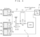
- a photovoltaic power generation system of the present embodiment includes a photovoltaic string 1, a power extractor 2, and a receiver 3 (see Figs. 1 and 2 ).
- the photovoltaic string 1 includes a plurality of photovoltaic modules 10 and a power line 11.
- a suffix is added to a reference numeral like a photovoltaic module 10N.
- a photovoltaic module 10 is simply referred to, it indicates any one photovoltaic module.
- a plurality of photovoltaic modules 10 are connected in series via the power line 11, and thus electric power obtained by photovoltaic cells is transmitted via the power line 11.
- each photovoltaic module 10 basically have the same configuration, the following description will proceed using one photovoltaic module 10 as an example.
- the configuration of each photovoltaic module may be changed if necessary.
- the photovoltaic module 10 includes a photovoltaic element 14 and a transmitter 15.
- the transmitter 15 corresponds to one specific example of the transmitting apparatus according to the present disclosure.
- the photovoltaic element 14 is understood as one power source as illustrated in Fig. 2 .
- the transmitter 15 includes a current source 151, a controller 152, and a bypass capacitor 153 (see Fig. 2 ). Further, the transmitter 15 of the present example additionally includes a transmitting diode 154 and a bypass diode 155.
- the current source 151 is connected to the power line 11 in parallel with the photovoltaic element 14. A specific configuration example of the current source will be described later.
- the current source 151 in this example is connected to the power line 11 to have the same current polarity as the photovoltaic element 14 connected in parallel to the current source 151.
- the controller 152 controls the current value in the current source 151 such that the current signal is generated.
- a microprocessor a micro-controller unit (MCU)
- MCU micro-controller unit
- the controller is not limited to this example as long as current value control (for example, on/off control) of the current source 151 is performed at a desired timing so that an appropriate current signal is generated.
- the bypass capacitor 153 is connected to the power line 11 in parallel with the photovoltaic element 14 and the current source 151.
- the current signal transmitted through the bypass capacitor 153 from a negative electrode side in the photovoltaic string 1 is transmitted to a positive electrode side (in a direction of an electric current I in Fig. 2 ).
- the transmitting diode 154 is connected between the current source 151 and the bypass capacitor 153.
- the electric current is prevented from being sent from the current source 151 to the bypass capacitor 153, and the electric current flows into the power line 11 accordingly.
- the bypass diode 155 is inserted in series between a (k-1)-th photovoltaic module and a (k+1)-th photovoltaic module.
- k is a number of a photovoltaic module of interest, and 1 ⁇ k ⁇ N in the present example.
- the bypass diode 155 allows the electric current to flow through the bypass diode 155 even when a certain failure occurs in a k-th photovoltaic module. Since the bypass diode 155 is constructed similarly to that used in the photovoltaic module of the related art further detailed description is omitted.
- the power extractor 2 is configured to extract electric power from the power line 11 using an inverter (specifically, a DC/AC inverter or a DC/DC converter). Any device can be used as the power extractor 2 as long as the electric power transmitted from the photovoltaic module 10 can be extracted from the power line 11. Since an existing device can be used as the power extractor of the present embodiment, further description is omitted.
- an inverter specifically, a DC/AC inverter or a DC/DC converter
- the receiver 3 is configured to receive the current signal transmitted from the transmitter 15 via the power line 11.
- the receiver 3 of the present example has a configuration capable of extracting a change in the current value as a signal using a current transformer CT. Detailed configuration of the receiver will be described later.
- the current signal it is possible to cause the current signal to be generated by switching the current source 151 (on/off switching).
- the current signal generated by the current source 151 is superimposed on the electric current flowing through the power line 11 and transmitted to the receiver 3.
- the transmitting diode 154 since the transmitting diode 154 is installed, the current signal from the current source 151 does not flow in the direction of the bypass capacitor 153. If a part of the current signal flows in the direction of the bypass capacitor 153, since a signal component passes through the capacitor, a noise rides on the power line 11 and the SN ratio of the current signal deteriorates. In the present embodiment, it is possible to improve the SN ratio of the current signal by suppressing the occurrence of such a noise.
- the current signal generated on an upstream side (for example, the (k-1)-th photovoltaic module) in an electric current direction is transmitted to the k-th photovoltaic module via the power line 11.
- This current signal passes through the bypass capacitor 153 and the transmitting diode 154 in the k-th photovoltaic module and is transmitted to a downstream side (for example, the (k+1)-th photovoltaic module).
- the photovoltaic element 14 is the current source
- the bypass capacitor 153 since the bypass capacitor 153 is not installed, the current signal is stopped by the current source and not transmitted to the downstream side.
- the bypass capacitor 153 since the bypass capacitor 153 is installed, it is possible to transmit the current signal to the downstream side.
- the current signal is transferred by the capacitor 153 without depending on the parasitic capacitance of the photovoltaic module, the SN ratio of the current signal is improved.
- the technology of the present embodiment can be applied even in a case in which the photovoltaic string 1 is connected in parallel and has an array configuration.
- the photovoltaic string 1 since a diode for backflow prevention is inserted, it is possible to prevent the current signal flowing through a certain string from flowing into another string. Therefore, even in the case of the array configuration, it is possible to detect by causing the current signal to flow in the direction of the receiver 3.
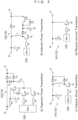
- FIG. 3(a) to 3(d) A further specific example of the current source 151 (including the controller 152) used in the transmitter 15 in the above embodiment will be described below with reference to Figs. 3(a) to 3(d) .
- common reference numerals such as a resistor R1 and a capacitor C1 are used, but an appropriate characteristic is employed in accordance with each circuit configuration.
- terminals a and b in Fig. 3 correspond to terminals a and b in Fig. 2 .
- a transmitter 15 (see Fig. 3(a) ) of a first example is of a capacitor pump type. This transmitter is configured to generate an electric current by using electric charges accumulated in a capacitor C2.
- the controller 152 (specifically, the microprocessor) turns on a transistor Q3 and turns off Q2 (that is, turns off Q1 eventually). Accordingly, the capacitor C2 is in a state in which electric charges are accumulated.
- the transistor Q3 is turned off, and Q2 is turned on (that is, Q1 is turned on accordingly).
- a potential of the capacitor C2 on a diode (D3 or D2) side rises to be nearly twice (because the potential of the capacitor C2 is added to the potential of the capacitor C1).
- the capacitor C2 transmits the electric current via the diode D3.
- the magnitude of the electric current is controlled in accordance with the electric current flowing through the transistor Q1.
- a current limiting diode D4 is connected to the transistor Q1 and controls the magnitude of the electric current flowing through the transistor Q1.
- the potential of the capacitor C1 decreases during pulse transmission (that is, during transmission of an ON waveform in the current signal), but since it is connected to the power source line via the resistor R1, the magnitude of the electric current drawn from the power source line is smaller than the magnitude of the electric current transmitted by the capacitor C2.
- the first example corresponds to one specific example of a "configuration in which the current source includes the pump capacitor that accumulates electric charges when the current signal is turned off and transmits the electric current to the power line when the current signal is turned on in accordance with a signal from the controller.”
- a transmitter 15 (see Fig. 3(b) ) of a second example can be called an inductor pump type.
- This transmitter 15 uses a capacitor C2 for pushing an electric current into a circuit.
- the controller 152 causes a transistor Q1 to be kept off.
- the controller 152 first turns on the transistor Q1 for a predetermined period time and then turns the transistor Q1 off.
- a coil L1 gradually draws an electric current from a capacitor C1.
- the transistor Q1 is turned off, the electric current from the coil L1 flows to the capacitor C2 via a diode D2 and increases a voltage thereof.
- a diode D3 is an electric current control diode which limits a maximum electric current generated by a transistor Q2.
- the transistor Q2 is turned off, and the current source 151 is turned off accordingly.
- a transmitter 15 (see Fig. 3(c) ) of a third example can be call a coil direct coupling type.
- This transmitter 15 is configured to generate an electric current using magnetic flux accumulated in a coil L1 (cause it to function as a current source).
- a transistor Q1 When the current source 151 is turned off, a transistor Q1 is turned off.
- the controller 152 first turns on the transistor Q1 for a certain period of time. Thereafter, the transistor Q1 is turned off. While the transistor Q1 is in the ON state, the coil L1 gradually draws an electric current from the capacitor C1 and functions as the current source.
- the transistor Q1 is turned OFF, the electric current is transmitted from the coil L1 via a diode D2. The electric current to be transmitted is stopped in due course (the current source 151 is regarded as being turned off accordingly).
- This third example corresponds to one specific example of a "configuration in which the current source includes a discharging coil, magnetic flux is accumulated by drawing the electric current in response to an ON signal from the controller, and the current signal is turned off after the electric current is transmitted to the power line for a period of time according to a time constant in response to an OFF signal from the controller.”
- a transmitter 15 (see Fig. 3(d) ) of a fourth example can be called a reverse electric current type.
- This transmitter 15 uses a transistor Q1 for drawing the electric current from the circuit, that is, for feeding an electric current of a opposite polarity to the circuit.
- the controller 152 switches to turn off the transistor Q1.
- the controller turns on the transistor Q1 via a resistor R 1.
- the resistor R1 by setting the resistor R1 to a large value appropriately, it is possible to limit the maximum electric current flowing through the transistor Q1. Note that, in this example, since a positive electrical current does not flow a direction from the current source 151 to the transmitting diode 154, installation of the transmitting diode 154 is omitted.
- the receiver 3 extracts a change in the electric current I (see Fig. 2 ) flowing through the circuit without contacting the power line 11 using the current transformer CT and extract a signal transmitted from the transmitter 15 by observing it through an AD converter ADC.
- a resistor R3 is attached between both contact points of the current transformer CT.
- a high frequency noise flowing through the power line 11 is cut by inserting a capacitor C2 between both ends of the current transformer CT. Further, since a low frequency noise is often in a band of about 50 Hz/60 Hz, it is removed by signal processing (differential processing) after AD conversion.
- an input voltage range of the AD converter ADC is 1.5 V to 3.5 V (that is, 1.5 V ⁇ VADC ⁇ 3.5 V).
- a smoothing step is necessary. This is because a pulse shape is not an exact rectangle, and the signal intensity varies depending on a configuration of the photovoltaic module. For this reason, the receiver of the present example calculates a smoothed value as follows.
- V t ⁇ 1 S t + 1 ⁇ ⁇ 1 V t ⁇ 1
- V avg t ⁇ 2 V t + 1 ⁇ ⁇ 2 V avg t ⁇ 1
- V max t max ⁇ V t , V avg t + MINDIFF , ⁇ 3 V max t ⁇ 1 ⁇ V avg t ⁇ 1 + V avg t ⁇ 1 ⁇ 0 ⁇ ⁇ 2 ⁇ ⁇ 1 ⁇ ⁇ 3 ⁇ 1
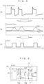
- S(t) indicates a sample value obtained by the AD converter ( Fig. 5(a) ), V(t) is a primary smoothed value, and Vmax(t) and Vavg(t) are smoothed values and given strength and an offset of a pulse signal ( Fig. 5(b) ).
- ⁇ 1, ⁇ 2, and ⁇ 3 in Formula are time constants.
- MINDIFF > 0 is a constant parameter, which gives the smallest difference between Vmax(t) and Vavg(t).
- a stage after smoothing is a pulse detection stage.
- a function active(t) is introduced. This is a function which becomes 1 when the pulse signal is active and becomes 0 in a case in which the pulse signal is not active. This function is implemented, for example, as follows.
- ⁇ (0 ⁇ ⁇ ⁇ 1) is a threshold value for pulse detection.
- a transmitter 15 used in a photovoltaic power generation system according to a second embodiment of the present disclosure will be described with reference to Fig. 6 .
- the same reference numerals are used for components which are basically common to components of the first embodiment to avoid complication of the description.
- the transmitting diode 154 is connected in series with the bypass capacitor 153. Further, the transmitter 15 includes a resistor R which is inserted in series with respect to the bypass capacitor 153 and in parallel with respect to the transmitting diode 154.
- a resistance value of the resistor R is set to a value necessary for causing the bypass capacitor to function.
- a model of a used photovoltaic element is SY-M12W-12 (available from SUNYOOO solar limited).
- An open circuit voltage is 21.8 V, and a short circuit current is 0.73 A.
- Maximum power is 12 W (at 17.4 V and 0.69 A).
- a load resistor in this experiment includes an input capacitance of 190 ⁇ F and a variable resistor whose resistance value is variable between 100 ⁇ and 600 ⁇ .
- the transmitter 15 was attached to a first (#1) photovoltaic module 10, and the current transformer CT of the receiver 3 was attached to a load portion. Further, in the experiments, the current sources 151 of different types (the respective types illustrated in Figs. 3(a) to 3(d) ) were used. Table 1 below shows values of parameters in the transmitter 15 and the receiver 3 used in this experiment example. In Table 1, the examples correspond to the examples of Figs. 3(a) to 3(d) in order from the top. Of course, these values are just an example, and the present disclosure is not limited by these values.
- ATmega 328 P-PU having a clock frequency of 16 MHz was used as the controller 152.
- An electrical characteristic of the photovoltaic module 10 depend on a situation of an I-V curve. For example, it is assumed that ⁇ , ⁇ , and ⁇ ( ⁇ ⁇ ⁇ ⁇ ⁇ ) indicate operating voltages of the photovoltaic module 10, and the voltage ⁇ corresponds to a maximum power point. At the voltage ⁇ , the photovoltaic module 10 operates as a constant current source, but at a voltage ⁇ , the photovoltaic module 10 operates as a constant voltage source.
- the change in the pulse waveform in the example using ten photovoltaic modules 10 connected in series was reviewed.
- Table 2 shows an operating voltage (V) in this experiment example. Of course, these are just an example, and the present disclosure is not limited thereto.
- Fig. 7 shows a result.
- a capacitor pump type illustrated in Fig. 7(a) a definite positive pulse with a magnitude of + 0.35 V and a negative pulse subsequent thereto were obtained.
- an inductor pump type illustrated in Fig. 7(b) initially, a negative voltage of -0.1 V was generated. This is probably because the electric current was charged to the coil. Thereafter, a slightly indefinite pulse of +0.3 V was generated for 200 ⁇ sec.
- a direct coil type illustrated in Fig. 7(c) a negative voltage of -1.0 V was similarly generated, but thereafter a definite large pulse of +7 V was generated for 200 ⁇ sec. Thereafter, a negative voltage pulse of -6 V was generated.
- a reverse voltage type illustrated in Fig. 7(d) a characteristic which is inverted upside down from that Fig. 7(a) was shown.
- FIGs. 8(a) to 8(c) illustrate three array configuration patterns.
- 20 ⁇ 1 is an array in which 20 panels are connected in series (that is, one as the photovoltaic string)
- 10 ⁇ 2 is an array in which two strings each including ten panels are arranged in parallel
- 5 ⁇ 4 is an array in which four strings each including five panels are arranged in parallel.
- a voltage giving the maximum power was used as the operating voltage. In other words, 348 V was used in the case of 20 ⁇ 1, 174 V was used in the case of 10 ⁇ 2, and 87 V was used in the case of 5 ⁇ 4.
- Figs. 9(a) to 9(d) The results are illustrated in Figs. 9(a) to 9(d) .
- a relation between the graphs and the type of the current source is similar to that in the case of Fig. 7 .
- the magnitude of the obtained pulse signal strength has a relation of 10 ⁇ 2 array > 20 ⁇ 1 array > 5 ⁇ 4 array.
- the signal strength exceeded a detection level. Therefore, it can be understood that the technology of the present disclosure can also be used for photovoltaic arrays constructed by arranging the photovoltaic strings in parallel.
- a data frame in this experiment example was set as follows. In other words, the data frame starts with an 8-bit signal 11111111. Subsequently, four bytes (for example, one byte is assigned to each for a panel ID, a voltage, an electric current, and a temperature) are continued. Finally, a checksum such as CRC 8 for error detection was inserted. A total length of the data frame is 48 bits. In this example, values of 1 and 0 are transmitted by inserting an interval of 1000 msec, and the transmitter 15 has generated a pulse of 500 ⁇ sec when the value was 1 and has not generated a pulse when the value was 0.
- the pulse is easily detected by the receiver 3.
- time synchronization is likely to be lost.
- the pulse modulation scheme described above is merely an example, and an appropriate modulation scheme such as pulse width modulation, pulse position modulation, or the like can be used.
- an appropriate modulation scheme such as pulse width modulation, pulse position modulation, or the like can be used.
- a scheme capable of distinguishing the signals as in a spreading coding scheme can be used.
- a combination of the transmitter and the receiver corresponds to a specific example of a monitoring apparatus in the present disclosure.
- a combination of the monitoring apparatus and the power extractor 2 that extracts the electric power transmitted via the power line corresponds to one specific example of the photovoltaic power generation system according to the present disclosure.
Landscapes
- Engineering & Computer Science (AREA)
- Power Engineering (AREA)
- Computer Networks & Wireless Communication (AREA)
- Signal Processing (AREA)
- Remote Monitoring And Control Of Power-Distribution Networks (AREA)
- Photovoltaic Devices (AREA)
- Cable Transmission Systems, Equalization Of Radio And Reduction Of Echo (AREA)
Claims (8)
- Übertragungsvorrichtung (15) zum Übertragen von Überwachungsinformation als ein Stromsignal in einem Photovoltaik-String (1), der eine Vielzahl von Photovoltaikelementen (14) enthält, die über eine Stromleitung (11) in Reihe miteinander geschaltet sind, wobei die Übertragungsvorrichtung (15) aufweist:eine Stromquelle (151);eine Steuereinheit (152); undeinen Bypass-Kondensator (153),wobei die Stromquelle (151) mit der Stromleitung (11) parallel geschaltet zu jedem der Photovoltaikelemente (14) verbunden ist,die Steuereinheit (152) dafür konfiguriert ist, einen Stromwert der Stromquelle (151) so zu steuern, dass das Stromsignal erzeugt wird, undder Bypass-Kondensator (153) parallel geschaltet zu jedem der Photovoltaikelemente (14) und zur Stromquelle (151) mit der Stromleitung (11) verbunden ist, so dass ein Stromsignal, das durch den Bypass-Kondensator (153) von einer negativen Elektrodenseite im Photovoltaik-String (1) übertragen wird, zu einer positiven Elektrodenseite übertragen wird.
- Übertragungsvorrichtung (15) nach Anspruch 1, wobei eine Strompolarität der mit der Stromleitung (11) verbundenen Stromquelle (151) die gleiche ist wie diejenige des Photovoltaikelements (14), zu dem die Stromquelle (151) parallel geschaltet ist.
- Übertragungsvorrichtung (15) nach Anspruch 1 oder 2, ferner mit einer Übertragungsdiode (154), die zwischen der Stromquelle (151) und dem Bypass-Kondensator (153) geschaltet ist, um zu verhindern, dass ein elektrischer Strom von der Stromquelle (151) zum Bypass-Kondensator (153) übertragen wird, und zum Einspeisen des elektrischen Stroms in die Stromleitung (11).
- Übertragungsvorrichtung (15) nach Anspruch 3, ferner mit einem Widerstand (R), der in Reihe mit dem Bypass-Kondensator (153) und parallel zur Übertragungsdiode (154) geschaltet ist.
- Übertragungsvorrichtung (15) nach einem der Ansprüche 1 bis 4, wobei die Stromquelle (151) einen Pumpkondensator (C1, C2) aufweist, der elektrische Ladungen akkumuliert, wenn das Stromsignal in Antwort auf ein Signal von der Steuereinheit (152) ausgeschaltet wird, und einen elektrischen Strom an die Stromleitung (11) überträgt, wenn das Stromsignal eingeschaltet ist.
- Übertragungsvorrichtung (15) nach einem der Ansprüche 1 bis 4, wobei die Stromquelle (151) eine Entladungsspule (L1) aufweist, die dafür konfiguriert ist, einen magnetischen Fluss durch Ziehen eines elektrischen Stroms in Antwort auf ein EIN-Signal von der Steuereinheit (152) zu akkumulieren, und das Stromsignal in Antwort auf ein AUS-Signal auszuschalten, nachdem der elektrische Strom von der Steuereinheit (152) für eine Zeitdauer, die einer Zeitkonstante der Entladungsspule (L1) entspricht, an die Stromleitung (11) übertragen wurde.
- Überwachungsvorrichtung, mit:der Übertragungsvorrichtung (15) nach einem der Ansprüche 1 bis 6; undeinem Empfänger (3), der dafür konfiguriert ist, das über die Stromleitung (11) übertragene Stromsignal zu empfangen.
- Photovoltaisches Stromerzeugungssystem, mit:der Überwachungsvorrichtung nach Anspruch 7; undeinem Stromextraktor (2), der über die Stromleitung (11) übertragenen elektrischen Strom extrahiert.
Applications Claiming Priority (2)
| Application Number | Priority Date | Filing Date | Title |
|---|---|---|---|
| JP2016130122A JP6710868B2 (ja) | 2016-06-30 | 2016-06-30 | 送信装置、受信装置、監視装置および太陽光発電システム |
| PCT/JP2017/023661 WO2018003825A1 (ja) | 2016-06-30 | 2017-06-28 | 太陽光ストリングにおける電流信号の送信装置 |
Publications (3)
| Publication Number | Publication Date |
|---|---|
| EP3480944A1 EP3480944A1 (de) | 2019-05-08 |
| EP3480944A4 EP3480944A4 (de) | 2019-11-13 |
| EP3480944B1 true EP3480944B1 (de) | 2023-10-18 |
Family
ID=60786710
Family Applications (1)
| Application Number | Title | Priority Date | Filing Date |
|---|---|---|---|
| EP17820179.4A Active EP3480944B1 (de) | 2016-06-30 | 2017-06-28 | Übertragungsvorrichtung für das stromsignal eines solarstrangs |
Country Status (5)
| Country | Link |
|---|---|
| US (1) | US10868493B2 (de) |
| EP (1) | EP3480944B1 (de) |
| JP (1) | JP6710868B2 (de) |
| CN (1) | CN109417361B (de) |
| WO (1) | WO2018003825A1 (de) |
Families Citing this family (3)
| Publication number | Priority date | Publication date | Assignee | Title |
|---|---|---|---|---|
| US11398749B2 (en) | 2017-05-22 | 2022-07-26 | Solaredge Technologies Ltd. | Method and apparatus to enable communication and control in a power system |
| CN110798246B (zh) * | 2019-09-29 | 2022-02-25 | 华为数字能源技术有限公司 | 一种应用于电力线通信的接口电路、组串及系统 |
| KR102396454B1 (ko) * | 2020-07-15 | 2022-05-09 | 충북대학교 산학협력단 | 진폭 및 주파수 변조를 통한 pv 팜에서의 개별 태양광 발전기 전력 측정 시스템 |
Family Cites Families (16)
| Publication number | Priority date | Publication date | Assignee | Title |
|---|---|---|---|---|
| JPH11251615A (ja) * | 1998-03-03 | 1999-09-17 | Canon Inc | 融雪機能付き太陽光発電システム |
| JP2007058843A (ja) * | 2005-07-27 | 2007-03-08 | Gunma Prefecture | 太陽光発電装置 |
| EP2249457A1 (de) | 2009-05-08 | 2010-11-10 | Nxp B.V. | PV-Solarzelle |
| WO2011133928A2 (en) * | 2010-04-22 | 2011-10-27 | Tigo Energy, Inc. | System and method for enhanced watch dog in solar panel installations |
| JP5419018B2 (ja) * | 2010-06-14 | 2014-02-19 | 独立行政法人産業技術総合研究所 | スペクトル拡散通信システム |
| CN202424315U (zh) * | 2011-12-27 | 2012-09-05 | 中电普瑞科技有限公司 | 一种灵活交流输电装置的控制保护系统 |
| JP5547311B1 (ja) | 2013-02-06 | 2014-07-09 | 株式会社日立アドバンストデジタル | 太陽光発電設備のための監視システム |
| DE102013101314A1 (de) * | 2013-02-11 | 2014-08-14 | Phoenix Contact Gmbh & Co. Kg | Sichere Photovoltaik-Anlage |
| KR20140123854A (ko) * | 2013-04-15 | 2014-10-23 | 한국전자통신연구원 | 직렬 연결된 전력선 통신 장치 및 방법 |
| JP6209412B2 (ja) * | 2013-09-27 | 2017-10-04 | 株式会社日立製作所 | 太陽光発電システムの故障診断システム及び故障診断方法 |
| US9947807B2 (en) * | 2014-02-06 | 2018-04-17 | Taiwan Semiconductor Manufacturing Co., Ltd. | Solar module with wireless power transfer |
| JP2015219675A (ja) * | 2014-05-16 | 2015-12-07 | 国立研究開発法人産業技術総合研究所 | 太陽電池の電力配分回路 |
| MA40029A (fr) * | 2014-05-27 | 2015-12-03 | Sunpower Corp | Protection de système photovoltaïque |
| US10218307B2 (en) * | 2014-12-02 | 2019-02-26 | Tigo Energy, Inc. | Solar panel junction boxes having integrated function modules |
| DE102016115295A1 (de) * | 2016-08-17 | 2018-02-22 | Sma Solar Technology Ag | Trennvorrichtung für einen photovoltaischen String |
| US20180102733A1 (en) * | 2016-10-06 | 2018-04-12 | Sohrab Peshoton Kakalia | Dynamic reconfiguration of solar panels based on light condition |
-
2016
- 2016-06-30 JP JP2016130122A patent/JP6710868B2/ja active Active
-
2017
- 2017-06-28 WO PCT/JP2017/023661 patent/WO2018003825A1/ja not_active Ceased
- 2017-06-28 US US16/313,949 patent/US10868493B2/en active Active
- 2017-06-28 EP EP17820179.4A patent/EP3480944B1/de active Active
- 2017-06-28 CN CN201780040175.7A patent/CN109417361B/zh active Active
Also Published As
| Publication number | Publication date |
|---|---|
| EP3480944A4 (de) | 2019-11-13 |
| JP2018007382A (ja) | 2018-01-11 |
| WO2018003825A1 (ja) | 2018-01-04 |
| US20190199282A1 (en) | 2019-06-27 |
| CN109417361B (zh) | 2021-06-29 |
| US10868493B2 (en) | 2020-12-15 |
| JP6710868B2 (ja) | 2020-06-17 |
| EP3480944A1 (de) | 2019-05-08 |
| CN109417361A (zh) | 2019-03-01 |
Similar Documents
| Publication | Publication Date | Title |
|---|---|---|
| US12348182B2 (en) | Safety switch for photovoltaic systems | |
| US10230310B2 (en) | Safety switch for photovoltaic systems | |
| CN102313873B (zh) | 电池节数检测电路及方法和监测系统 | |
| US9472961B2 (en) | Method of forming a balancing circuit for a plurality of battery cells and structure therefor | |
| US10197608B2 (en) | Apparatus for determining insulation resistance at a PV generator, and photovoltaic installation | |
| DE112009001793T5 (de) | Leistungsumwandlungsvorrichtung | |
| CN102156504A (zh) | 一种太阳能电池板最大功率跟踪装置、跟踪方法以及应用其的太阳能供电装置 | |
| CN106169925A (zh) | 具有输出均流的单片集成电路开关器件 | |
| DE102014103450A1 (de) | Leistungswandlerschaltung, die wenigstens eine Batterie aufweist | |
| CN105896980A (zh) | 恒定导通时间控制的直流-直流变换器以及多相电源 | |
| EP3480944A1 (de) | Übertragungsvorrichtung für das stromsignal eines solarstrangs | |
| CN114189132B (zh) | 用于功率因数校正的控制方法和电路 | |
| WO2012155325A1 (en) | Dc/dc power converter with wide input voltage range | |
| CN110958743B (zh) | 一种开路和对地短路保护的电路和方法 | |
| CN105939148A (zh) | 一种光伏电池监测装置 | |
| CN110086143A (zh) | 输入电压分压电路和过压保护开关 | |
| DE102005033477B4 (de) | Schaltungsanordnung und Verfahren zum Konvertieren einer Wechselspannung in eine gleichgerichtete Spannung | |
| CN106655823B (zh) | 一种抗磁干扰的开关电源及其控制电路和控制方法 | |
| CN208608900U (zh) | 电力转换器控制电路 | |
| WO2020242786A1 (en) | Techniques for controlling a single-inductor multiple-output (simo) switched-mode power supply (smps) | |
| CN218473026U (zh) | 一种宽范围输入的芯片启动电路 | |
| CN115615273B (zh) | 电子雷管充电电流自适应调节方法和系统 | |
| CN114660337A (zh) | 高压脉冲电源和功率半导体测试装置 | |
| CN217739419U (zh) | 动力电池的高压采样电路和系统 | |
| CN115483813B (zh) | 一种交直流自适应输入采样电路和开关电源 |
Legal Events
| Date | Code | Title | Description |
|---|---|---|---|
| STAA | Information on the status of an ep patent application or granted ep patent |
Free format text: STATUS: THE INTERNATIONAL PUBLICATION HAS BEEN MADE |
|
| PUAI | Public reference made under article 153(3) epc to a published international application that has entered the european phase |
Free format text: ORIGINAL CODE: 0009012 |
|
| STAA | Information on the status of an ep patent application or granted ep patent |
Free format text: STATUS: REQUEST FOR EXAMINATION WAS MADE |
|
| 17P | Request for examination filed |
Effective date: 20190128 |
|
| AK | Designated contracting states |
Kind code of ref document: A1 Designated state(s): AL AT BE BG CH CY CZ DE DK EE ES FI FR GB GR HR HU IE IS IT LI LT LU LV MC MK MT NL NO PL PT RO RS SE SI SK SM TR |
|
| AX | Request for extension of the european patent |
Extension state: BA ME |
|
| DAV | Request for validation of the european patent (deleted) | ||
| DAX | Request for extension of the european patent (deleted) | ||
| A4 | Supplementary search report drawn up and despatched |
Effective date: 20191010 |
|
| RIC1 | Information provided on ipc code assigned before grant |
Ipc: H02J 13/00 20060101ALI20191004BHEP Ipc: H02S 50/00 20140101AFI20191004BHEP |
|
| STAA | Information on the status of an ep patent application or granted ep patent |
Free format text: STATUS: EXAMINATION IS IN PROGRESS |
|
| 17Q | First examination report despatched |
Effective date: 20210827 |
|
| GRAP | Despatch of communication of intention to grant a patent |
Free format text: ORIGINAL CODE: EPIDOSNIGR1 |
|
| STAA | Information on the status of an ep patent application or granted ep patent |
Free format text: STATUS: GRANT OF PATENT IS INTENDED |
|
| INTG | Intention to grant announced |
Effective date: 20230510 |
|
| GRAS | Grant fee paid |
Free format text: ORIGINAL CODE: EPIDOSNIGR3 |
|
| P01 | Opt-out of the competence of the unified patent court (upc) registered |
Effective date: 20230807 |
|
| GRAA | (expected) grant |
Free format text: ORIGINAL CODE: 0009210 |
|
| STAA | Information on the status of an ep patent application or granted ep patent |
Free format text: STATUS: THE PATENT HAS BEEN GRANTED |
|
| AK | Designated contracting states |
Kind code of ref document: B1 Designated state(s): AL AT BE BG CH CY CZ DE DK EE ES FI FR GB GR HR HU IE IS IT LI LT LU LV MC MK MT NL NO PL PT RO RS SE SI SK SM TR |
|
| REG | Reference to a national code |
Ref country code: GB Ref legal event code: FG4D |
|
| REG | Reference to a national code |
Ref country code: CH Ref legal event code: EP |
|
| REG | Reference to a national code |
Ref country code: IE Ref legal event code: FG4D |
|
| REG | Reference to a national code |
Ref country code: DE Ref legal event code: R096 Ref document number: 602017075506 Country of ref document: DE |
|
| REG | Reference to a national code |
Ref country code: LT Ref legal event code: MG9D |
|
| REG | Reference to a national code |
Ref country code: NL Ref legal event code: MP Effective date: 20231018 |
|
| REG | Reference to a national code |
Ref country code: AT Ref legal event code: MK05 Ref document number: 1623368 Country of ref document: AT Kind code of ref document: T Effective date: 20231018 |
|
| PG25 | Lapsed in a contracting state [announced via postgrant information from national office to epo] |
Ref country code: NL Free format text: LAPSE BECAUSE OF FAILURE TO SUBMIT A TRANSLATION OF THE DESCRIPTION OR TO PAY THE FEE WITHIN THE PRESCRIBED TIME-LIMIT Effective date: 20231018 |
|
| PG25 | Lapsed in a contracting state [announced via postgrant information from national office to epo] |
Ref country code: GR Free format text: LAPSE BECAUSE OF FAILURE TO SUBMIT A TRANSLATION OF THE DESCRIPTION OR TO PAY THE FEE WITHIN THE PRESCRIBED TIME-LIMIT Effective date: 20240119 |
|
| PG25 | Lapsed in a contracting state [announced via postgrant information from national office to epo] |
Ref country code: IS Free format text: LAPSE BECAUSE OF FAILURE TO SUBMIT A TRANSLATION OF THE DESCRIPTION OR TO PAY THE FEE WITHIN THE PRESCRIBED TIME-LIMIT Effective date: 20240218 |
|
| PG25 | Lapsed in a contracting state [announced via postgrant information from national office to epo] |
Ref country code: LT Free format text: LAPSE BECAUSE OF FAILURE TO SUBMIT A TRANSLATION OF THE DESCRIPTION OR TO PAY THE FEE WITHIN THE PRESCRIBED TIME-LIMIT Effective date: 20231018 |
|
| PG25 | Lapsed in a contracting state [announced via postgrant information from national office to epo] |
Ref country code: AT Free format text: LAPSE BECAUSE OF FAILURE TO SUBMIT A TRANSLATION OF THE DESCRIPTION OR TO PAY THE FEE WITHIN THE PRESCRIBED TIME-LIMIT Effective date: 20231018 |
|
| PG25 | Lapsed in a contracting state [announced via postgrant information from national office to epo] |
Ref country code: ES Free format text: LAPSE BECAUSE OF FAILURE TO SUBMIT A TRANSLATION OF THE DESCRIPTION OR TO PAY THE FEE WITHIN THE PRESCRIBED TIME-LIMIT Effective date: 20231018 |
|
| PG25 | Lapsed in a contracting state [announced via postgrant information from national office to epo] |
Ref country code: LT Free format text: LAPSE BECAUSE OF FAILURE TO SUBMIT A TRANSLATION OF THE DESCRIPTION OR TO PAY THE FEE WITHIN THE PRESCRIBED TIME-LIMIT Effective date: 20231018 Ref country code: IS Free format text: LAPSE BECAUSE OF FAILURE TO SUBMIT A TRANSLATION OF THE DESCRIPTION OR TO PAY THE FEE WITHIN THE PRESCRIBED TIME-LIMIT Effective date: 20240218 Ref country code: GR Free format text: LAPSE BECAUSE OF FAILURE TO SUBMIT A TRANSLATION OF THE DESCRIPTION OR TO PAY THE FEE WITHIN THE PRESCRIBED TIME-LIMIT Effective date: 20240119 Ref country code: ES Free format text: LAPSE BECAUSE OF FAILURE TO SUBMIT A TRANSLATION OF THE DESCRIPTION OR TO PAY THE FEE WITHIN THE PRESCRIBED TIME-LIMIT Effective date: 20231018 Ref country code: BG Free format text: LAPSE BECAUSE OF FAILURE TO SUBMIT A TRANSLATION OF THE DESCRIPTION OR TO PAY THE FEE WITHIN THE PRESCRIBED TIME-LIMIT Effective date: 20240118 Ref country code: AT Free format text: LAPSE BECAUSE OF FAILURE TO SUBMIT A TRANSLATION OF THE DESCRIPTION OR TO PAY THE FEE WITHIN THE PRESCRIBED TIME-LIMIT Effective date: 20231018 Ref country code: PT Free format text: LAPSE BECAUSE OF FAILURE TO SUBMIT A TRANSLATION OF THE DESCRIPTION OR TO PAY THE FEE WITHIN THE PRESCRIBED TIME-LIMIT Effective date: 20240219 |
|
| PG25 | Lapsed in a contracting state [announced via postgrant information from national office to epo] |
Ref country code: SE Free format text: LAPSE BECAUSE OF FAILURE TO SUBMIT A TRANSLATION OF THE DESCRIPTION OR TO PAY THE FEE WITHIN THE PRESCRIBED TIME-LIMIT Effective date: 20231018 Ref country code: RS Free format text: LAPSE BECAUSE OF FAILURE TO SUBMIT A TRANSLATION OF THE DESCRIPTION OR TO PAY THE FEE WITHIN THE PRESCRIBED TIME-LIMIT Effective date: 20231018 Ref country code: PL Free format text: LAPSE BECAUSE OF FAILURE TO SUBMIT A TRANSLATION OF THE DESCRIPTION OR TO PAY THE FEE WITHIN THE PRESCRIBED TIME-LIMIT Effective date: 20231018 Ref country code: NO Free format text: LAPSE BECAUSE OF FAILURE TO SUBMIT A TRANSLATION OF THE DESCRIPTION OR TO PAY THE FEE WITHIN THE PRESCRIBED TIME-LIMIT Effective date: 20240118 Ref country code: LV Free format text: LAPSE BECAUSE OF FAILURE TO SUBMIT A TRANSLATION OF THE DESCRIPTION OR TO PAY THE FEE WITHIN THE PRESCRIBED TIME-LIMIT Effective date: 20231018 Ref country code: HR Free format text: LAPSE BECAUSE OF FAILURE TO SUBMIT A TRANSLATION OF THE DESCRIPTION OR TO PAY THE FEE WITHIN THE PRESCRIBED TIME-LIMIT Effective date: 20231018 |
|
| PG25 | Lapsed in a contracting state [announced via postgrant information from national office to epo] |
Ref country code: DK Free format text: LAPSE BECAUSE OF FAILURE TO SUBMIT A TRANSLATION OF THE DESCRIPTION OR TO PAY THE FEE WITHIN THE PRESCRIBED TIME-LIMIT Effective date: 20231018 |
|
| REG | Reference to a national code |
Ref country code: DE Ref legal event code: R097 Ref document number: 602017075506 Country of ref document: DE |
|
| PG25 | Lapsed in a contracting state [announced via postgrant information from national office to epo] |
Ref country code: CZ Free format text: LAPSE BECAUSE OF FAILURE TO SUBMIT A TRANSLATION OF THE DESCRIPTION OR TO PAY THE FEE WITHIN THE PRESCRIBED TIME-LIMIT Effective date: 20231018 |
|
| PG25 | Lapsed in a contracting state [announced via postgrant information from national office to epo] |
Ref country code: SK Free format text: LAPSE BECAUSE OF FAILURE TO SUBMIT A TRANSLATION OF THE DESCRIPTION OR TO PAY THE FEE WITHIN THE PRESCRIBED TIME-LIMIT Effective date: 20231018 |
|
| PG25 | Lapsed in a contracting state [announced via postgrant information from national office to epo] |
Ref country code: SM Free format text: LAPSE BECAUSE OF FAILURE TO SUBMIT A TRANSLATION OF THE DESCRIPTION OR TO PAY THE FEE WITHIN THE PRESCRIBED TIME-LIMIT Effective date: 20231018 Ref country code: SK Free format text: LAPSE BECAUSE OF FAILURE TO SUBMIT A TRANSLATION OF THE DESCRIPTION OR TO PAY THE FEE WITHIN THE PRESCRIBED TIME-LIMIT Effective date: 20231018 Ref country code: RO Free format text: LAPSE BECAUSE OF FAILURE TO SUBMIT A TRANSLATION OF THE DESCRIPTION OR TO PAY THE FEE WITHIN THE PRESCRIBED TIME-LIMIT Effective date: 20231018 Ref country code: IT Free format text: LAPSE BECAUSE OF FAILURE TO SUBMIT A TRANSLATION OF THE DESCRIPTION OR TO PAY THE FEE WITHIN THE PRESCRIBED TIME-LIMIT Effective date: 20231018 Ref country code: EE Free format text: LAPSE BECAUSE OF FAILURE TO SUBMIT A TRANSLATION OF THE DESCRIPTION OR TO PAY THE FEE WITHIN THE PRESCRIBED TIME-LIMIT Effective date: 20231018 Ref country code: DK Free format text: LAPSE BECAUSE OF FAILURE TO SUBMIT A TRANSLATION OF THE DESCRIPTION OR TO PAY THE FEE WITHIN THE PRESCRIBED TIME-LIMIT Effective date: 20231018 Ref country code: CZ Free format text: LAPSE BECAUSE OF FAILURE TO SUBMIT A TRANSLATION OF THE DESCRIPTION OR TO PAY THE FEE WITHIN THE PRESCRIBED TIME-LIMIT Effective date: 20231018 |
|
| PLBE | No opposition filed within time limit |
Free format text: ORIGINAL CODE: 0009261 |
|
| STAA | Information on the status of an ep patent application or granted ep patent |
Free format text: STATUS: NO OPPOSITION FILED WITHIN TIME LIMIT |
|
| 26N | No opposition filed |
Effective date: 20240719 |
|
| PG25 | Lapsed in a contracting state [announced via postgrant information from national office to epo] |
Ref country code: SI Free format text: LAPSE BECAUSE OF FAILURE TO SUBMIT A TRANSLATION OF THE DESCRIPTION OR TO PAY THE FEE WITHIN THE PRESCRIBED TIME-LIMIT Effective date: 20231018 |
|
| PG25 | Lapsed in a contracting state [announced via postgrant information from national office to epo] |
Ref country code: SI Free format text: LAPSE BECAUSE OF FAILURE TO SUBMIT A TRANSLATION OF THE DESCRIPTION OR TO PAY THE FEE WITHIN THE PRESCRIBED TIME-LIMIT Effective date: 20231018 |
|
| PG25 | Lapsed in a contracting state [announced via postgrant information from national office to epo] |
Ref country code: MC Free format text: LAPSE BECAUSE OF FAILURE TO SUBMIT A TRANSLATION OF THE DESCRIPTION OR TO PAY THE FEE WITHIN THE PRESCRIBED TIME-LIMIT Effective date: 20231018 |
|
| REG | Reference to a national code |
Ref country code: CH Ref legal event code: PL |
|
| PG25 | Lapsed in a contracting state [announced via postgrant information from national office to epo] |
Ref country code: LU Free format text: LAPSE BECAUSE OF NON-PAYMENT OF DUE FEES Effective date: 20240628 |
|
| GBPC | Gb: european patent ceased through non-payment of renewal fee |
Effective date: 20240628 |
|
| PG25 | Lapsed in a contracting state [announced via postgrant information from national office to epo] |
Ref country code: IE Free format text: LAPSE BECAUSE OF NON-PAYMENT OF DUE FEES Effective date: 20240628 |
|
| PG25 | Lapsed in a contracting state [announced via postgrant information from national office to epo] |
Ref country code: BE Free format text: LAPSE BECAUSE OF NON-PAYMENT OF DUE FEES Effective date: 20240630 Ref country code: CH Free format text: LAPSE BECAUSE OF NON-PAYMENT OF DUE FEES Effective date: 20240630 |
|
| PG25 | Lapsed in a contracting state [announced via postgrant information from national office to epo] |
Ref country code: FR Free format text: LAPSE BECAUSE OF NON-PAYMENT OF DUE FEES Effective date: 20240630 |
|
| PG25 | Lapsed in a contracting state [announced via postgrant information from national office to epo] |
Ref country code: GB Free format text: LAPSE BECAUSE OF NON-PAYMENT OF DUE FEES Effective date: 20240628 |
|
| REG | Reference to a national code |
Ref country code: BE Ref legal event code: MM Effective date: 20240630 |
|
| PGFP | Annual fee paid to national office [announced via postgrant information from national office to epo] |
Ref country code: DE Payment date: 20250625 Year of fee payment: 9 |
|
| PG25 | Lapsed in a contracting state [announced via postgrant information from national office to epo] |
Ref country code: FI Free format text: LAPSE BECAUSE OF FAILURE TO SUBMIT A TRANSLATION OF THE DESCRIPTION OR TO PAY THE FEE WITHIN THE PRESCRIBED TIME-LIMIT Effective date: 20231019 |
|
| PG25 | Lapsed in a contracting state [announced via postgrant information from national office to epo] |
Ref country code: CY Free format text: LAPSE BECAUSE OF FAILURE TO SUBMIT A TRANSLATION OF THE DESCRIPTION OR TO PAY THE FEE WITHIN THE PRESCRIBED TIME-LIMIT; INVALID AB INITIO Effective date: 20170628 |
|
| PG25 | Lapsed in a contracting state [announced via postgrant information from national office to epo] |
Ref country code: HU Free format text: LAPSE BECAUSE OF FAILURE TO SUBMIT A TRANSLATION OF THE DESCRIPTION OR TO PAY THE FEE WITHIN THE PRESCRIBED TIME-LIMIT; INVALID AB INITIO Effective date: 20170628 |