EP3480833A1 - Schmallückige koplanare abstimmbare kondensatoren und verfahren zur herstellung davon - Google Patents
Schmallückige koplanare abstimmbare kondensatoren und verfahren zur herstellung davon Download PDFInfo
- Publication number
- EP3480833A1 EP3480833A1 EP18202148.5A EP18202148A EP3480833A1 EP 3480833 A1 EP3480833 A1 EP 3480833A1 EP 18202148 A EP18202148 A EP 18202148A EP 3480833 A1 EP3480833 A1 EP 3480833A1
- Authority
- EP
- European Patent Office
- Prior art keywords
- layer
- dielectric layer
- voltage
- inter
- tunable
- Prior art date
- Legal status (The legal status is an assumption and is not a legal conclusion. Google has not performed a legal analysis and makes no representation as to the accuracy of the status listed.)
- Granted
Links
- 239000003990 capacitor Substances 0.000 title claims abstract description 106
- 238000000034 method Methods 0.000 title claims description 47
- 238000004519 manufacturing process Methods 0.000 title description 25
- 125000006850 spacer group Chemical group 0.000 claims abstract description 98
- 239000000758 substrate Substances 0.000 claims abstract description 36
- BASFCYQUMIYNBI-UHFFFAOYSA-N platinum Chemical compound [Pt] BASFCYQUMIYNBI-UHFFFAOYSA-N 0.000 claims description 96
- 238000000151 deposition Methods 0.000 claims description 60
- 229910052751 metal Inorganic materials 0.000 claims description 53
- 239000002184 metal Substances 0.000 claims description 53
- VYPSYNLAJGMNEJ-UHFFFAOYSA-N Silicium dioxide Chemical compound O=[Si]=O VYPSYNLAJGMNEJ-UHFFFAOYSA-N 0.000 claims description 48
- 229910052697 platinum Inorganic materials 0.000 claims description 42
- 229910052454 barium strontium titanate Inorganic materials 0.000 claims description 38
- 239000000463 material Substances 0.000 claims description 38
- 238000005530 etching Methods 0.000 claims description 35
- 238000001465 metallisation Methods 0.000 claims description 27
- 239000000377 silicon dioxide Substances 0.000 claims description 24
- 235000012239 silicon dioxide Nutrition 0.000 claims description 24
- RTAQQCXQSZGOHL-UHFFFAOYSA-N Titanium Chemical compound [Ti] RTAQQCXQSZGOHL-UHFFFAOYSA-N 0.000 claims description 9
- VNSWULZVUKFJHK-UHFFFAOYSA-N [Sr].[Bi] Chemical compound [Sr].[Bi] VNSWULZVUKFJHK-UHFFFAOYSA-N 0.000 claims description 6
- 239000000956 alloy Substances 0.000 claims description 6
- 229910045601 alloy Inorganic materials 0.000 claims description 6
- 229910052741 iridium Inorganic materials 0.000 claims description 6
- 229910052746 lanthanum Inorganic materials 0.000 claims description 6
- FZLIPJUXYLNCLC-UHFFFAOYSA-N lanthanum atom Chemical compound [La] FZLIPJUXYLNCLC-UHFFFAOYSA-N 0.000 claims description 6
- 239000000203 mixture Substances 0.000 claims description 6
- IQONKZQQCCPWMS-UHFFFAOYSA-N barium lanthanum Chemical compound [Ba].[La] IQONKZQQCCPWMS-UHFFFAOYSA-N 0.000 claims description 5
- 230000004888 barrier function Effects 0.000 claims description 5
- NKZSPGSOXYXWQA-UHFFFAOYSA-N dioxido(oxo)titanium;lead(2+) Chemical compound [Pb+2].[O-][Ti]([O-])=O NKZSPGSOXYXWQA-UHFFFAOYSA-N 0.000 claims description 5
- KJTLSVCANCCWHF-UHFFFAOYSA-N Ruthenium Chemical compound [Ru] KJTLSVCANCCWHF-UHFFFAOYSA-N 0.000 claims description 4
- GKOZUEZYRPOHIO-UHFFFAOYSA-N iridium atom Chemical compound [Ir] GKOZUEZYRPOHIO-UHFFFAOYSA-N 0.000 claims description 4
- 229910052762 osmium Inorganic materials 0.000 claims description 4
- SYQBFIAQOQZEGI-UHFFFAOYSA-N osmium atom Chemical compound [Os] SYQBFIAQOQZEGI-UHFFFAOYSA-N 0.000 claims description 4
- 229910052707 ruthenium Inorganic materials 0.000 claims description 4
- PNEYBMLMFCGWSK-UHFFFAOYSA-N Alumina Chemical compound [O-2].[O-2].[O-2].[Al+3].[Al+3] PNEYBMLMFCGWSK-UHFFFAOYSA-N 0.000 claims description 2
- XUIMIQQOPSSXEZ-UHFFFAOYSA-N Silicon Chemical compound [Si] XUIMIQQOPSSXEZ-UHFFFAOYSA-N 0.000 claims description 2
- 239000000919 ceramic Substances 0.000 claims description 2
- 239000011521 glass Substances 0.000 claims description 2
- 239000000395 magnesium oxide Substances 0.000 claims description 2
- CPLXHLVBOLITMK-UHFFFAOYSA-N magnesium oxide Inorganic materials [Mg]=O CPLXHLVBOLITMK-UHFFFAOYSA-N 0.000 claims description 2
- AXZKOIWUVFPNLO-UHFFFAOYSA-N magnesium;oxygen(2-) Chemical compound [O-2].[Mg+2] AXZKOIWUVFPNLO-UHFFFAOYSA-N 0.000 claims description 2
- 229910052594 sapphire Inorganic materials 0.000 claims description 2
- 239000010980 sapphire Substances 0.000 claims description 2
- 239000010703 silicon Substances 0.000 claims description 2
- 229910052710 silicon Inorganic materials 0.000 claims description 2
- 230000008021 deposition Effects 0.000 description 35
- 230000008569 process Effects 0.000 description 14
- 239000003989 dielectric material Substances 0.000 description 8
- 238000000059 patterning Methods 0.000 description 8
- 230000010354 integration Effects 0.000 description 6
- NRTOMJZYCJJWKI-UHFFFAOYSA-N Titanium nitride Chemical compound [Ti]#N NRTOMJZYCJJWKI-UHFFFAOYSA-N 0.000 description 4
- 230000000694 effects Effects 0.000 description 4
- 238000005516 engineering process Methods 0.000 description 4
- 238000002360 preparation method Methods 0.000 description 3
- 239000010409 thin film Substances 0.000 description 3
- 229910000838 Al alloy Inorganic materials 0.000 description 2
- 229910052782 aluminium Inorganic materials 0.000 description 2
- 230000015572 biosynthetic process Effects 0.000 description 2
- 238000010586 diagram Methods 0.000 description 2
- PCHJSUWPFVWCPO-UHFFFAOYSA-N gold Chemical compound [Au] PCHJSUWPFVWCPO-UHFFFAOYSA-N 0.000 description 2
- 229910052737 gold Inorganic materials 0.000 description 2
- 239000010931 gold Substances 0.000 description 2
- 238000002955 isolation Methods 0.000 description 2
- 229910052451 lead zirconate titanate Inorganic materials 0.000 description 2
- GQYHUHYESMUTHG-UHFFFAOYSA-N lithium niobate Chemical compound [Li+].[O-][Nb](=O)=O GQYHUHYESMUTHG-UHFFFAOYSA-N 0.000 description 2
- 238000001459 lithography Methods 0.000 description 2
- 150000002739 metals Chemical class 0.000 description 2
- 150000004767 nitrides Chemical class 0.000 description 2
- 238000000206 photolithography Methods 0.000 description 2
- 230000008439 repair process Effects 0.000 description 2
- 229910052581 Si3N4 Inorganic materials 0.000 description 1
- 229910002353 SrRuO3 Inorganic materials 0.000 description 1
- 230000006978 adaptation Effects 0.000 description 1
- XAGFODPZIPBFFR-UHFFFAOYSA-N aluminium Chemical compound [Al] XAGFODPZIPBFFR-UHFFFAOYSA-N 0.000 description 1
- 238000005452 bending Methods 0.000 description 1
- RZEADQZDBXGRSM-UHFFFAOYSA-N bismuth lanthanum Chemical compound [La].[Bi] RZEADQZDBXGRSM-UHFFFAOYSA-N 0.000 description 1
- 230000015556 catabolic process Effects 0.000 description 1
- 230000001413 cellular effect Effects 0.000 description 1
- 239000011248 coating agent Substances 0.000 description 1
- 238000000576 coating method Methods 0.000 description 1
- 238000004891 communication Methods 0.000 description 1
- 229910052802 copper Inorganic materials 0.000 description 1
- 238000005137 deposition process Methods 0.000 description 1
- AMGQUBHHOARCQH-UHFFFAOYSA-N indium;oxotin Chemical compound [In].[Sn]=O AMGQUBHHOARCQH-UHFFFAOYSA-N 0.000 description 1
- ODNHQUQWHMGWGT-UHFFFAOYSA-N iridium;oxotin Chemical compound [Ir].[Sn]=O ODNHQUQWHMGWGT-UHFFFAOYSA-N 0.000 description 1
- HFGPZNIAWCZYJU-UHFFFAOYSA-N lead zirconate titanate Chemical compound [O-2].[O-2].[O-2].[O-2].[O-2].[Ti+4].[Zr+4].[Pb+2] HFGPZNIAWCZYJU-UHFFFAOYSA-N 0.000 description 1
- 238000002161 passivation Methods 0.000 description 1
- 229910021420 polycrystalline silicon Inorganic materials 0.000 description 1
- 229920001690 polydopamine Polymers 0.000 description 1
- 229920005591 polysilicon Polymers 0.000 description 1
- 229910052706 scandium Inorganic materials 0.000 description 1
- SIXSYDAISGFNSX-UHFFFAOYSA-N scandium atom Chemical compound [Sc] SIXSYDAISGFNSX-UHFFFAOYSA-N 0.000 description 1
- HQVNEWCFYHHQES-UHFFFAOYSA-N silicon nitride Chemical compound N12[Si]34N5[Si]62N3[Si]51N64 HQVNEWCFYHHQES-UHFFFAOYSA-N 0.000 description 1
- 239000006104 solid solution Substances 0.000 description 1
- 238000005477 sputtering target Methods 0.000 description 1
- 238000006467 substitution reaction Methods 0.000 description 1
- 229910052719 titanium Inorganic materials 0.000 description 1
- 239000010936 titanium Substances 0.000 description 1
Images


Classifications
-
- H—ELECTRICITY
- H01—ELECTRIC ELEMENTS
- H01L—SEMICONDUCTOR DEVICES NOT COVERED BY CLASS H10
- H01L28/00—Passive two-terminal components without a potential-jump or surface barrier for integrated circuits; Details thereof; Multistep manufacturing processes therefor
- H01L28/40—Capacitors
- H01L28/60—Electrodes
-
- H—ELECTRICITY
- H01—ELECTRIC ELEMENTS
- H01G—CAPACITORS; CAPACITORS, RECTIFIERS, DETECTORS, SWITCHING DEVICES, LIGHT-SENSITIVE OR TEMPERATURE-SENSITIVE DEVICES OF THE ELECTROLYTIC TYPE
- H01G4/00—Fixed capacitors; Processes of their manufacture
- H01G4/002—Details
- H01G4/018—Dielectrics
- H01G4/06—Solid dielectrics
- H01G4/08—Inorganic dielectrics
- H01G4/12—Ceramic dielectrics
- H01G4/1209—Ceramic dielectrics characterised by the ceramic dielectric material
- H01G4/1218—Ceramic dielectrics characterised by the ceramic dielectric material based on titanium oxides or titanates
- H01G4/1227—Ceramic dielectrics characterised by the ceramic dielectric material based on titanium oxides or titanates based on alkaline earth titanates
-
- H—ELECTRICITY
- H01—ELECTRIC ELEMENTS
- H01G—CAPACITORS; CAPACITORS, RECTIFIERS, DETECTORS, SWITCHING DEVICES, LIGHT-SENSITIVE OR TEMPERATURE-SENSITIVE DEVICES OF THE ELECTROLYTIC TYPE
- H01G4/00—Fixed capacitors; Processes of their manufacture
- H01G4/33—Thin- or thick-film capacitors
-
- H—ELECTRICITY
- H01—ELECTRIC ELEMENTS
- H01G—CAPACITORS; CAPACITORS, RECTIFIERS, DETECTORS, SWITCHING DEVICES, LIGHT-SENSITIVE OR TEMPERATURE-SENSITIVE DEVICES OF THE ELECTROLYTIC TYPE
- H01G7/00—Capacitors in which the capacitance is varied by non-mechanical means; Processes of their manufacture
- H01G7/06—Capacitors in which the capacitance is varied by non-mechanical means; Processes of their manufacture having a dielectric selected for the variation of its permittivity with applied voltage, i.e. ferroelectric capacitors
-
- H—ELECTRICITY
- H01—ELECTRIC ELEMENTS
- H01L—SEMICONDUCTOR DEVICES NOT COVERED BY CLASS H10
- H01L21/00—Processes or apparatus adapted for the manufacture or treatment of semiconductor or solid state devices or of parts thereof
- H01L21/02—Manufacture or treatment of semiconductor devices or of parts thereof
- H01L21/04—Manufacture or treatment of semiconductor devices or of parts thereof the devices having potential barriers, e.g. a PN junction, depletion layer or carrier concentration layer
- H01L21/18—Manufacture or treatment of semiconductor devices or of parts thereof the devices having potential barriers, e.g. a PN junction, depletion layer or carrier concentration layer the devices having semiconductor bodies comprising elements of Group IV of the Periodic Table or AIIIBV compounds with or without impurities, e.g. doping materials
- H01L21/28—Manufacture of electrodes on semiconductor bodies using processes or apparatus not provided for in groups H01L21/20 - H01L21/268
- H01L21/283—Deposition of conductive or insulating materials for electrodes conducting electric current
-
- H—ELECTRICITY
- H01—ELECTRIC ELEMENTS
- H01L—SEMICONDUCTOR DEVICES NOT COVERED BY CLASS H10
- H01L21/00—Processes or apparatus adapted for the manufacture or treatment of semiconductor or solid state devices or of parts thereof
- H01L21/02—Manufacture or treatment of semiconductor devices or of parts thereof
- H01L21/04—Manufacture or treatment of semiconductor devices or of parts thereof the devices having potential barriers, e.g. a PN junction, depletion layer or carrier concentration layer
- H01L21/18—Manufacture or treatment of semiconductor devices or of parts thereof the devices having potential barriers, e.g. a PN junction, depletion layer or carrier concentration layer the devices having semiconductor bodies comprising elements of Group IV of the Periodic Table or AIIIBV compounds with or without impurities, e.g. doping materials
- H01L21/30—Treatment of semiconductor bodies using processes or apparatus not provided for in groups H01L21/20 - H01L21/26
- H01L21/31—Treatment of semiconductor bodies using processes or apparatus not provided for in groups H01L21/20 - H01L21/26 to form insulating layers thereon, e.g. for masking or by using photolithographic techniques; After treatment of these layers; Selection of materials for these layers
- H01L21/3105—After-treatment
- H01L21/311—Etching the insulating layers by chemical or physical means
- H01L21/31105—Etching inorganic layers
- H01L21/31111—Etching inorganic layers by chemical means
-
- H—ELECTRICITY
- H01—ELECTRIC ELEMENTS
- H01L—SEMICONDUCTOR DEVICES NOT COVERED BY CLASS H10
- H01L21/00—Processes or apparatus adapted for the manufacture or treatment of semiconductor or solid state devices or of parts thereof
- H01L21/02—Manufacture or treatment of semiconductor devices or of parts thereof
- H01L21/04—Manufacture or treatment of semiconductor devices or of parts thereof the devices having potential barriers, e.g. a PN junction, depletion layer or carrier concentration layer
- H01L21/18—Manufacture or treatment of semiconductor devices or of parts thereof the devices having potential barriers, e.g. a PN junction, depletion layer or carrier concentration layer the devices having semiconductor bodies comprising elements of Group IV of the Periodic Table or AIIIBV compounds with or without impurities, e.g. doping materials
- H01L21/30—Treatment of semiconductor bodies using processes or apparatus not provided for in groups H01L21/20 - H01L21/26
- H01L21/31—Treatment of semiconductor bodies using processes or apparatus not provided for in groups H01L21/20 - H01L21/26 to form insulating layers thereon, e.g. for masking or by using photolithographic techniques; After treatment of these layers; Selection of materials for these layers
- H01L21/3205—Deposition of non-insulating-, e.g. conductive- or resistive-, layers on insulating layers; After-treatment of these layers
- H01L21/321—After treatment
- H01L21/3213—Physical or chemical etching of the layers, e.g. to produce a patterned layer from a pre-deposited extensive layer
- H01L21/32133—Physical or chemical etching of the layers, e.g. to produce a patterned layer from a pre-deposited extensive layer by chemical means only
-
- H—ELECTRICITY
- H01—ELECTRIC ELEMENTS
- H01L—SEMICONDUCTOR DEVICES NOT COVERED BY CLASS H10
- H01L23/00—Details of semiconductor or other solid state devices
- H01L23/52—Arrangements for conducting electric current within the device in operation from one component to another, i.e. interconnections, e.g. wires, lead frames
- H01L23/522—Arrangements for conducting electric current within the device in operation from one component to another, i.e. interconnections, e.g. wires, lead frames including external interconnections consisting of a multilayer structure of conductive and insulating layers inseparably formed on the semiconductor body
- H01L23/5222—Capacitive arrangements or effects of, or between wiring layers
- H01L23/5223—Capacitor integral with wiring layers
-
- H—ELECTRICITY
- H01—ELECTRIC ELEMENTS
- H01L—SEMICONDUCTOR DEVICES NOT COVERED BY CLASS H10
- H01L23/00—Details of semiconductor or other solid state devices
- H01L23/52—Arrangements for conducting electric current within the device in operation from one component to another, i.e. interconnections, e.g. wires, lead frames
- H01L23/522—Arrangements for conducting electric current within the device in operation from one component to another, i.e. interconnections, e.g. wires, lead frames including external interconnections consisting of a multilayer structure of conductive and insulating layers inseparably formed on the semiconductor body
- H01L23/528—Geometry or layout of the interconnection structure
-
- H—ELECTRICITY
- H01—ELECTRIC ELEMENTS
- H01L—SEMICONDUCTOR DEVICES NOT COVERED BY CLASS H10
- H01L28/00—Passive two-terminal components without a potential-jump or surface barrier for integrated circuits; Details thereof; Multistep manufacturing processes therefor
- H01L28/40—Capacitors
- H01L28/55—Capacitors with a dielectric comprising a perovskite structure material
- H01L28/56—Capacitors with a dielectric comprising a perovskite structure material the dielectric comprising two or more layers, e.g. comprising buffer layers, seed layers, gradient layers
-
- H—ELECTRICITY
- H01—ELECTRIC ELEMENTS
- H01L—SEMICONDUCTOR DEVICES NOT COVERED BY CLASS H10
- H01L28/00—Passive two-terminal components without a potential-jump or surface barrier for integrated circuits; Details thereof; Multistep manufacturing processes therefor
- H01L28/40—Capacitors
- H01L28/60—Electrodes
- H01L28/75—Electrodes comprising two or more layers, e.g. comprising a barrier layer and a metal layer
-
- H—ELECTRICITY
- H01—ELECTRIC ELEMENTS
- H01L—SEMICONDUCTOR DEVICES NOT COVERED BY CLASS H10
- H01L28/00—Passive two-terminal components without a potential-jump or surface barrier for integrated circuits; Details thereof; Multistep manufacturing processes therefor
- H01L28/40—Capacitors
- H01L28/60—Electrodes
- H01L28/82—Electrodes with an enlarged surface, e.g. formed by texturisation
- H01L28/90—Electrodes with an enlarged surface, e.g. formed by texturisation having vertical extensions
- H01L28/92—Electrodes with an enlarged surface, e.g. formed by texturisation having vertical extensions made by patterning layers, e.g. by etching conductive layers
-
- H—ELECTRICITY
- H01—ELECTRIC ELEMENTS
- H01G—CAPACITORS; CAPACITORS, RECTIFIERS, DETECTORS, SWITCHING DEVICES, LIGHT-SENSITIVE OR TEMPERATURE-SENSITIVE DEVICES OF THE ELECTROLYTIC TYPE
- H01G4/00—Fixed capacitors; Processes of their manufacture
- H01G4/002—Details
- H01G4/018—Dielectrics
- H01G4/06—Solid dielectrics
- H01G4/08—Inorganic dielectrics
- H01G4/12—Ceramic dielectrics
- H01G4/1209—Ceramic dielectrics characterised by the ceramic dielectric material
- H01G4/1236—Ceramic dielectrics characterised by the ceramic dielectric material based on zirconium oxides or zirconates
-
- H—ELECTRICITY
- H01—ELECTRIC ELEMENTS
- H01G—CAPACITORS; CAPACITORS, RECTIFIERS, DETECTORS, SWITCHING DEVICES, LIGHT-SENSITIVE OR TEMPERATURE-SENSITIVE DEVICES OF THE ELECTROLYTIC TYPE
- H01G4/00—Fixed capacitors; Processes of their manufacture
- H01G4/002—Details
- H01G4/018—Dielectrics
- H01G4/06—Solid dielectrics
- H01G4/08—Inorganic dielectrics
- H01G4/12—Ceramic dielectrics
- H01G4/1209—Ceramic dielectrics characterised by the ceramic dielectric material
- H01G4/1254—Ceramic dielectrics characterised by the ceramic dielectric material based on niobium or tungsteen, tantalum oxides or niobates, tantalates
Definitions
- the subject disclosure relates to U.S. Patent Application entitled TUNABLE COPLANAR CAPACITOR WITH VERTICAL TUNING AND LATERAL RF PATH AND METHODS FOR MANUFACTURING THEREOF, in the name of Marina Zelner, et al., filed on the same date as the present application, having attorney docket number 50409-ID_10209-0156, the disclosure of which is hereby incorporated by reference.
- the subject disclosure relates, in general, to coplanar tunable capacitors and, more particularly, to small-gap coplanar tunable capacitors and methods for manufacturing thereof.
- Tunable capacitors have various uses in RF systems including as voltage-tunable devices. Some benefits of tunable capacitors are integration of different values and functions of capacitance. Applications for tunable capacitors can include tunable filters, voltage controlled oscillators, tunable phase shifters, tunable matching networks, low-impedance power supplies, decoupling high-frequency signals at an IC bonding pad, or others.
- Integrated circuits including tunable capacitors can, for example, be used in portable electronics for low-power wireless communication (e.g., cellular phones, pagers, PDAs, and so forth), directional antenna systems, high clock-rate microphones, miniature DC to DC converters, or other devices.
- low-power wireless communication e.g., cellular phones, pagers, PDAs, and so forth
- directional antenna systems e.g., cellular phones, pagers, PDAs, and so forth
- high clock-rate microphones e.g., high clock-rate microphones, miniature DC to DC converters, or other devices.
- the subject disclosure describes, among other things, illustrative embodiments of coplanar tunable capacitors and methods for manufacturing thereof. Other embodiments are described by the subject disclosure.
- One embodiment of the subject disclosure includes a coplanar capacitor, comprising: a substrate; a voltage-tunable dielectric layer over the substrate; a plurality of bias lines over the voltage-tunable dielectric layer, wherein each of the plurality of bias lines includes vertical sidewalls, and wherein the plurality of bias lines are covered by an inter-level dielectric; a plurality of sidewall spacers, each of the plurality of sidewall spacers being located adjacent to and in intimate contact with a respective vertical sidewall of one of the plurality of bias lines and the inter-level dielectric; and a metal electrode over the inter-level dielectric, and over portions of the voltage-tunable dielectric layer that are not covered by the plurality of bias lines and that are not covered by the sidewall spacers, wherein a plurality of gaps are etched in the metal electrode to insulate and separate portions of metal electrode over the voltage-tunable dielectric layer from each other but still completely cover the exposed portions of the voltage-tunable dielectric layer.
- a coplanar capacitor comprising: a first dielectric layer, wherein the first dielectric layer is disposed on a substrate, wherein the substrate includes a silicon dioxide layer upon which the first dielectric layer is disposed, and wherein the first dielectric layer comprises a voltage-tunable dielectric; a plurality of bias lines, wherein each of the plurality of bias lines includes vertical sidewalls, and wherein the plurality of bias lines are disposed on the voltage-tunable dielectric layer, and wherein the plurality of bias lines comprise metal; an inter-level dielectric, wherein the inter-level dielectric is disposed on the plurality of bias lines; a plurality of sidewall spacers, wherein each of the plurality of sidewall spacers is located adjacent to and in intimate contact with a respective vertical sidewall of one of the plurality of bias lines; and a metal electrode layer, wherein the electrode layer is disposed on portions of the voltage-tunable dielectric layer that are not covered by the plurality of bias lines and that are not covered by the
- Another embodiment of the subject disclosure includes a method for fabricating a coplanar capacitor, the method comprising: depositing a voltage-tunable dielectric layer on a substrate; depositing a metal layer on the voltage-tunable dielectric layer; depositing an inter-level dielectric layer on the metal layer; etching material from the inter-level dielectric layer and from the metal layer to form a plurality of bias lines covered at least partially by respective portions of the inter-level dielectric layer, wherein each of the plurality of bias lines includes vertical sidewalls; depositing an oxide layer on exposed surface portions of the inter-level dielectric layer and on exposed surface portions of the voltage-tunable dielectric layer, wherein the oxide layer that is deposited includes upright portions between the inter-level dielectric layer and the voltage-tunable dielectric layer; etching material from the oxide layer to expose portions of the inter-level dielectric layer, to expose portions of the voltage-tunable dielectric layer and to form, from the upright portions, a plurality of sidewall spacers, wherein each of the plurality of sidewall space
- Another embodiment of the subject disclosure includes a method for fabricating a coplanar capacitor, the method comprising: depositing a first dielectric layer, wherein the first dielectric layer is deposited on a substrate including a silicon dioxide layer; depositing a first metal layer, wherein the first metal layer is deposited on the first dielectric layer; depositing a second dielectric layer, wherein the second dielectric layer is deposited on the first metal layer; forming a plurality of bias lines by etching material from the second dielectric layer and from the first metal layer, wherein the plurality of bias lines are covered at least partially by respective portions of the second dielectric layer, and wherein each of the plurality of bias lines includes vertical sidewalls, and; depositing an oxide layer, wherein some of the oxide layer is deposited on exposed surface portions of the second dielectric layer, wherein some the oxide layer is deposited on exposed surface portions of the first dielectric layer, and wherein some of the oxide layer forms upright portions between the second dielectric layer and the first dielectric layer; exposing, via etching of material from
- FIG. 1 a coplanar tunable capacitor device 101 according to an embodiment is shown (this FIG. 1 shows the device 101 in cross section).
- Device 101 comprises substrate 103 (including thin silicon dioxide layer 105).
- a voltage-tunable dielectric layer 107 is disposed over the substrate, on the thin silicon dioxide layer (in another embodiment, the voltage-tunable dielectric layer can be disposed directly on the substrate (without the thin silicon dioxide layer being disposed between the two)).
- the voltage-tunable material can have a dielectric constant that can be varied by application of a voltage.
- a plurality of bias lines 109A, 109B are disposed over the voltage-tunable dielectric layer (while two bias lines are shown in this view, it is to be understood that any desired number of bias lines may be utilized). Further, the plurality of bias lines are covered by respective portions 111A, 111B of an inter-level dielectric.
- the voltage-tunable material can comprise one or more of a high-K ferroelectric material, such as (but not limited to) barium strontium titanate (BST), lead zirconate titanate (PZT), lead lanthanum zirconate titanate (PLZT), strontium bismuth tantalate (SBT), lithium niobate (LN), bismuth lanthanum titanate (BLT), and lead scandium titanate including doped compositions or solid solutions thereof.
- a high-K ferroelectric material such as (but not limited to) barium strontium titanate (BST), lead zirconate titanate (PZT), lead lanthanum zirconate titanate (PLZT), strontium bismuth tantalate (SBT), lithium niobate (LN), bismuth lanthanum titanate (BLT), and lead scandium titanate including doped compositions or solid solutions thereof.
- BST barium strontium titanate
- PZT lead zirconate
- a plurality of sidewall spacers 113A, 113B, 113C and 113D are provided.
- Each of the plurality of sidewall spacers is located adjacent one of the plurality of bias lines and each of the plurality of sidewall spacers spans between a respective portion of the voltage-tunable dielectric layer and a respective portion of the inter-level dielectric.
- an electrode 115 e.g., an RF electrode
- ILD inter-level dielectric
- electrode 115 can include layer 112 (e.g. a thin platinum layer).
- a plurality of gaps 117A, 117B are disposed in the electrode, wherein each of the plurality of gaps is located at a location above a respective one of the plurality of bias lines.
- a left-right dimension (see, e.g., the horizontal distance between points 1A and 1B in this view) of a sidewall spacer can be about 2,000-3,000 angstroms (inclusive). It is these sidewall spacer lateral dimensions that are sub-micron and that define the dielectric thickness of the capacitor. A left-right dimension in this range can be provided as described herein without use of submicron lithography.
- a signal e.g., an RF signal
- a signal can be injected at the left side of device 101 and propagate to the right side of the device 101 and/or a signal (e.g., an RF signal) can be injected at the right side of device 101 and propagate to the left side of the device 101.
- a width of the gap 117A can impact the Q factor for device 101.
- a positive voltage can be applied at bias line 109A (and/or at bias line 109B) and the electrode 115 can be biased to DC ground.
- a sidewall configuration disclosed herein can reduce electrostrictive resonance (for example, electrostrictive resonance effects can be reduced because such waves would move laterally without encountering interfaces that can reflect and cause losses in the device at specific frequency).
- a sidewall configuration disclosed herein can be used to define a tunable capacitor on top of a barium strontium titanate (BST) layer (in this regard, see “A", "B” C” and “D” of FIG. 1 showing tunable lateral capacitor areas (coplanar) under sidewall spacers).
- the sidewalls can reduce the tuning voltage of the coplanar capacitor (e.g., reducing the tuning voltage from approximately 200V to approximately 24V, depending on the width of the sidewall spacers).
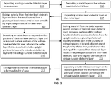
- step 203 comprises depositing a voltage-tunable dielectric layer on a substrate.
- step 205 comprises depositing a metal layer on the voltage-tunable dielectric layer.
- step 207 comprises depositing an inter-level dielectric layer on the metal layer.
- step 209 comprises etching material from the inter-level dielectric layer and from the metal layer to form a plurality of bias lines covered at least partially by respective portions of the inter-level dielectric layer (in one specific example, the etch gives vertical or near-vertical sidewalls on the inter-level dielectric and the metal bias lines).
- step 211 comprises depositing a conformal oxide layer on the whole surface.
- This conformal oxide layer has a lateral thickness (of the deposited oxide layer) on the vertical sidewalls of the etched inter-level dielectric and the etched metal bias line substantially the same as the vertical thickness (of the deposited oxide layer) on the horizontal surfaces of the inter-level dielectric and the voltage-tunable dielectric.
- step 213 comprises etching (anisotropically etching) material from the oxide layer to expose portions of the inter-level dielectric layer, to expose portions of the voltage-tunable dielectric layer and to form, from the upright portions, a plurality of sidewall spacers, wherein each of the plurality of sidewall spacers is located adjacent one of the plurality of bias lines, and wherein the etching of the material from the oxide layer results in exposed portions of the inter-level dielectric layer and exposed portions of the voltage-tunable dielectric layer.
- the etching of this step forms an insulating layer (e.g., the sidewall spacers) of well-defined thickness from the deposited oxide on each vertical sidewall of the inter-level dielectric layer and metal layer.
- step 215 comprises depositing a metal interconnect layer on the exposed portions of the inter-level dielectric layer and on the exposed the portions of the voltage-tunable dielectric layer.
- step 217 comprises etching material from the interconnect layer to form a plurality of gaps.
- the interconnect layer (see step 215) can be deposited over the portions of the inter-level dielectric layer by being deposited on portions of the oxide layer that remain above the inter-level dielectric layer.
- the etching the material from the oxide layer can comprise performing anisotropic etching.
- the anisotropic etching can be in a direction perpendicular to the substrate.
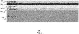
- FIG. 3 depicts the results of: (a) substrate preparation (see substrate 303 (which can include thereon a field oxide layer 305); (b) voltage-tunable dielectric deposition (see dielectric 307); (c) platinum (Pt) deposition (see metal 309); (d) ILD oxide deposition (see ILD oxide 311).
- the voltage-tunable dielectric can also be patterned.
- the voltage-tunable dielectric can be doped BST.
- the voltage-tunable dielectric can be sputtered.
- the voltage-tunable dielectric can be annealed.
- FIG. 4 depicts the results of: (a) bias line platinum pattern (see 309 formed by etching out sections of platinum); followed by (b) a high-temperature anneal to repair the voltage-tunable dielectric.
- the bias line "width" (as shown left-right in this view) should be minimized (i.e., made as small as possible).
- the bias line "width” can impact the capacitance.
- the bias line "length" that is, into the page in this view
- the number of bias lines can impact the capacitance.
- FIG. 5 depicts the results of: (a) resistor oxide deposition (see 313); (b) SiCr process; and (c) spacer oxide deposition (see 313).
- conformal deposition of the resistor oxide and the spacer oxide to the outer surfaces of the platinum (309) facilitates the production of sidewall spacers (see 314A, 314B, 314C and 314D of FIG. 6 ) that are conformal.
- the term conformal can include "mirroring" a surface.
- each sidewall can have the same longitudinal thickness at a given height.
- the resistor oxide deposition and the spacer oxide deposition could be the same process but the SiCr processing sequence could go as follows: (1) resistor oxide deposition (conformal); (2) SiCr deposition; (3) SiCr patterning/etch; (4) SiCr anneal (for final resistance); (5) spacer oxide deposition (conformal).
- the resistors are patterned to leave the resistor patterns separated from the active area of the device.
- FIG. 6 depicts the results of: (a) resistor/via contact, sidewall spacer (see 314A, 314B, 314C and 314D) etch and (b) via anneal.
- the etch is anisotropic (e.g., vertical (or substantially vertical) as shown up-down in this view).
- the via anneal is a high temperature anneal that is performed after the sidewall etch to repair the dielectric 307 and to remove any residue.
- FIG. 7 depicts production of an RF electrode resulting from: (a) deposition of platinum layer 312; and (b) deposition of M1 (metal) layer 315.
- the platinum layer can be a thin layer.
- the RF electrode can comprise the M1 metal layer (without the platinum layer 312).
- the M1 layer stack can comprise titanium-nitride (TiN), titanium, aluminum, TiN, gold, or any combination thereof.
- TiN titanium-nitride
- M1 can refer to "Metal 1," which is generally known as the first metal interconnect layer on an integrated circuit. In other examples, other M1 materials such as different alloys and layers may be used.
- the TiN functions as a barrier between the BST and the Al.
- Pt can be the metal of choice for the first layer of M1 for BST because of its high work function that gives the lowest leakage of all metals, though other elements such as Ir can be used as well.
- FIG. 8 (related to M1/platinum (RF electrode) pattern/etch) depicts production of gaps 317A, 317B in the RF electrode by patterning/etching the M1 layer 315 and the platinum layer 312. In one specific example, the patterning/etching produces minimum Al lines/spaces.
- FIGs. 9A-9G , 10A-10G and 11A-11G depict an illustrative embodiment of various steps in the manufacturing of a coplanar capacitor (the views of FIGs. 9A-9G provide lateral cross-sections and these views include a resistor; the views of FIGs. 10A-10G provide cross-sections through a bias line; the views of FIGs. 11A-11G provide cross-sections through the RF electrode).
- each call out number refers to the same respective component (as modified throughout the process).
- each call out number refers to the same respective component of FIGs. 9A-9G (as modified throughout the process).
- FIGs. 11A-11G each call out number refers to the same respective component of FIGs. 9A-9G (as modified throughout the process).
- substrate 903 includes a thin silicon dioxide layer 905.
- a voltage-tunable dielectric layer 907 is disposed over the substrate, on the thin silicon dioxide layer.
- a plurality of bias lines are disposed over the voltage-tunable dielectric layer. Further, the plurality of bias lines are covered by respective portions of an inter-level dielectric 911.
- a plurality of sidewall spacers are provided. Each of the plurality of sidewall spacers is formed from an oxide layer 913 and is located adjacent one of the plurality of bias lines. Each of the plurality of sidewall spacers spans between a respective portion of the voltage-tunable dielectric layer and a respective portion of the inter-level dielectric such that the bias lines are fully enclosed in oxide.
- an electrode 915 e.g., an RF electrode
- ILD inter-level dielectric
- electrode 915 can include layer 912 (e.g. a thin platinum layer).
- a plurality of gaps are disposed in the electrode, wherein each of the plurality of gaps is located at a location above a respective one of the plurality of bias lines.
- FIG. 9A relates to voltage-tunable dielectric/Pt bias line material/inter-level dielectric deposition
- FIG. 9B relates to pattern/etch of the above stack (optional but useful).
- FIG. 9C relates to bias line pattern/etch: vertical sidewalls
- FIG. 9D relates to resistor oxide deposition, SiCr dep/pattern/etch/anneal (see resistor 950 - any desired number of which may be provided)
- FIG. 9E relates to spacer oxide deposition, spacer pattern/etch, Via pattern/etch
- FIG. 9F relates to M1 stack deposition
- FIG. 9G relates to M1 pattern/etch.
- FIG. 10A relates to substrate preparation and BST/platinum/ILD deposition
- FIG. 10B relates to BST patterning
- FIG. 10C relates to bias line patterning and high-temperature anneal
- FIG. 10D relates to resistor oxide deposition and SiCr deposition/anneal etch
- FIG. 10E relates to spacer oxide deposition, SiCr contact etch, spacer/via etch (anisotropic) and via anneal
- FIG. 10F relates to platinum/M1 deposition
- FIG. 10G relates to M1/platinum etch.
- FIGs. 10D-10G do not show the right-most portions of the device, with such deleted portions indicated in these FIGs. by three ellipses defined.
- FIG. 11A relates to substrate preparation and BST/platinum/ILD deposition
- FIG. 11B relates to BST patterning
- FIG. 11C relates to bias line patterning and high-temperature anneal
- FIG. 11D relates to resistor oxide deposition and SiCr deposition/anneal etch
- FIG. 11E relates to spacer oxide deposition, SiCr contact etch, spacer/via etch (anisotropic) and via anneal
- FIG. 11F relates to platinum/M1 deposition
- FIG. 11G relates to M1/platinum etch.
- FIGs. 11D-11G do not show the right-most portions of the device, with such deleted portions indicated in these FIGs. by three ellipses defined.
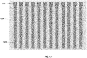
- FIG. 12 this depicts an illustrative embodiment related to manufacture of a coplanar capacitor at the stage of the process shown in FIG. 4 (this FIG. 12 is a top-down view). This view is after a platinum/BST etch and after an ILD/platinum bias line etch. Shown in this FIG. 12 is voltage-tunable dielectric 1207, a plurality of bias lines (only one of which - 1209 has a call out number), and a plurality of via pads (only one of which - 1210 has a call out number).
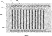
- FIG. 13 this depicts an illustrative embodiment related to manufacture of a coplanar capacitor (this FIG. 13 is a top-down view). This view is after resistor oxide deposition, SiCr processing, spacer oxide deposition, spacer etch and via processing. Shown in this FIG. 13 is the voltage-tunable dielectric 1307, a plurality of bias lines (only one of which - 1309 has a call out number), spacer oxide 1310, SiCr resistors 1313, SiCr resistor contacts 1315, and bias line contacts 1317.
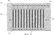
- FIG. 14 this depicts an illustrative embodiment related to manufacture of a coplanar capacitor (this FIG. 14 is a top-down view). This view is after M1 deposition/etch. Shown in this FIG. 14 is a location for RF input 1407, a location for RF output 1409, and a location for providing DC bias 1410. Also shown in this FIG. 14
- M1/SiCr see, e.g., 1413
- M1/bias line contacts see, e.g., 1415
- RF electrode/SiCr resistor contacts see, e.g., 1417
- active capacitor areas under the spacers see, e.g., active capacitor areas 1419 under M1 on the side of the bias lines.
- FIG. 15 this depicts an illustrative embodiment related to manufacture of a coplanar capacitor (this FIG. 15 is a top-down view). This view is with SiCr directly contacting the platinum bias lines. Shown in this FIG. 15 is a location for RF input 1507, a location for RF output 1509, and a location for providing bias 1510. Also shown in this FIG. 15 are direct SiCr/Pt bias line contacts (see, e.g., 1513).
- various embodiments provide: (a) isolation of the RF electrode from the bias lines (using sidewall spacers); (b) definition of the active capacitor dielectric thickness (using sidewall spacers) and (c) passivation of the active (e.g., PARASCAN) capacitor dielectric (an unpassivated device may not be reliable and may fail in the field).
- active e.g., PARASCAN
- SGCC small-gap coplanar capacitors
- platinum Pt
- M1 RF electrode and Pt bias line can be interchanged with the bias line having the thin Pt/TiN/A1 and the RF electrode having the thick Pt and M1 on top.
- SiCr resistors can integrate easily into the technology. Such resistors may be needed to isolate the DC bias supply from the RF signal (as in a conventional Paratek Tunable Integrated Capacitors.
- the initial ILD (which can comprise, for example, silicon dioxide) can be necessary to isolate the bias line from the Pt/M1 RF electrode (or vice-versa). Without this isolation the spacer etch would, in certain manufacturing embodiments, expose the bias line Pt and short out the capacitor.
- sidewall spacers can be formed from structures with vertical edges covered with a conformal coating and etched using an anisotropic selective etch.
- a relatively thicker platinum layer can be used for the bias lines and a relatively thinner platinum and/or /M1 layer can be used only for the RF electrodes.
- the converse relative thicknesses can be provided.
- the bias line width can be an influence on Q-factor by introducing extra series resistance.
- the design must guarantee that no voltage-tunable dielectric is exposed after the M1 patterning.
- the bias line width is determined by the minimum M1 space and the M1/bias line alignment tolerance minus the spacer width. With good lithography and etch this could be, for example, less than 6um (in this example, the length of the bias line could still be very high so there should be minimal impact on Q).
- resistor integration can include one or more of the following: (a) resistor oxide and spacer oxide are conformal; (b) etch the resistor and bias line vias (BLV's) together down to SiCr; BLV's will be only partially etched; (c) spacer etch will be patterned: leave oxide covering the edge of the BST and open the BLV's to platinum; leave resist on the SiCr contacts to protect against the spacer etch; the capacitor width is defined by the spacer oxide opening.
- M1 can be used to seal all open BST after spacer etch.
- standard barrier/nitride/M2 or bump finish can be applied after M1 (as used in certain conventional processes).
- M2 can refer to the second layer of metal in a multi-layer interconnect technology.
- both low and high voltage capacitors can be provided in the same technology.
- the platinum makes a workable contact for the SiCr then the following simplifications can be provided: do the bias line via pattern/etch, SiCr deposition/anneal pattern, spacer oxide deposition, resistor contact pattern/etch, spacer pattern/etch (protecting the SiCr contacts), Pt/M1 deposition /etch.
- the process can use 7 masks: BST, Bias line, Resistor, Resistor/Bias line Via, Spacer, M1, Overcoat.
- the process can use 8 masks with M2, 9 masks with a pre-patterned lower electrode/BST mask for parallel-plate tunable capacitor integration.
- the lower electrode could also be used as another interconnect.
- the BST mask could be unnecessary (but its use could add a lot of flexibility in the device design - e.g., the chip could have co-planar waveguide (CPW) structures, nitride caps, etc.).
- CPW co-planar waveguide
- a patterned lower electrode could be done with another mask.
- the BST mask would then cut off the damaged BST at the edges of the electrode, allowing a parallel plate BST capacitor to be fabricated alongside the coplanar capacitor(s) with additional layers of BST (and masks) if required.
- the use of a sidewall spacer together with BST to define (without deep-submicron photolithography) a lateral capacitor width in the BST layer is provided.
- the BST can be PARASCAN and/or one or more other ferroelectric/polar/paraelectric tunable dielectrics.
- a sidewall spacer to separate a bias electrode from an RF electrode.
- the bias and RF electrodes can be formed from one or more of Pt, Al alloys, Al alloys combined with conductive barrier metals or alloys, gold, Ir, Ir oxides, SrRuO3, other conductive, resistive or semiconductive materials.
- bias line width and RF electrode width to optimize the RF performance of the lateral capacitor (e.g., specifically optimize for electrostrictive resonance and third harmonic effects).
- integration of parallel-plate and coplanar BST capacitors in the same chip can be provided.
- the other dielectrics can include one or more of silicon nitride, silicon dioxide.
- microwave RF structures such as coplanar waveguides, phase shifters, power splitters/combiners, mixers, etc.
- coplanar BST capacitors and/or parallel-plate capacitors can be provided.
- non-linear behavior of the capacitor can be minimized and/or harmonics that potentially limit the applications of the capacitor can be minimized.
- capacitors can be provided that are useable at very high frequencies.
- capacitors can be provided to cancel out effects such as electrostrictive resonance and third-order harmonics.
- a coplanar capacitor (with reasonable tuning voltage and usable capacitance) can be produced without requiring sophisticated and expensive photolithography.
- sidewall spacer technology can be used to create a narrow gap of tunable material (e.g. PARASCAN) in a coplanar structure. This can provide a low and controlled tuning voltage and higher capacitance (e.g., relative to other coplanar capacitor structures).
- various capacitor components are disposed laterally on a surface.
- capacitors that are coplanar structures and that include sidewall spacers.
- capacitors and methods of making capacitors where sidewall spacers are formed to create a narrow gap of tunable dielectric material in a coplanar structure.
- the sidewall spacers can separate a bias electrode from an RF electrode.
- Configurations according to various embodiments can give a low and controlled tuning voltage and higher capacitance relative to certain other coplanar capacitor structures.
- deposition of the resistor oxide and/or the spacer oxide can result in a conformal configuration.
- the device/method can require only one tunable dielectric and the capacitor dielectric can be electrically stacked to allow multiple capacitors in series (e.g., for cancellation of resonances and/or odd harmonics).
- the coplanar structure can allow different configurations of capacitors which can help reduce electrostrictive resonance and higher-level harmonic effects.
- the structure can also be integrated with coplanar waveguides and/or other thin-film microwave structures (e.g., to form compact integrated microwave circuits with good high frequency performance).
- a resistor can be comprised of any thin film resistor material.
- a resistor can be comprised of polysilicon.
- a resistor can be comprised of indium-tin-oxide (ITO).
- ITO indium-tin-oxide
- the ILD can isolate the M1 (e.g., metal, Al, Cu) from the bias lines.
- M1 e.g., metal, Al, Cu
- a sufficiently thick ILD may permit a relatively thin bias line platinum layer.
- use of platinum for the bias lines can keep the capacitor leakage low.
- a resistor may connect to each bias line.
- a resistive material e.g., iridium tin oxide
- platinum can replace the platinum as the bias line material.
- a coplanar capacitor can be provided with components rigidly in a common plane (e.g., rigidly connected to a planar substrate).
- a coplanar capacitor can be provided such that there is essentially no flexing or bending provided or allowed between the components thereof.
- any desired voltage-tunable dielectrics may be utilized (e.g., not just PARASCAN or its derivatives (such derivatives being, for example, PARASCAN-like voltage tunable dielectrics)).
- undoped BST may be utilized for the voltage-tunable dielectric.
- the electrodes can comprise any desired and appropriate material or materials.
- the Pt/M1 is etched to give the RF electrodes and the interconnect lines for the device.
- the gaps will define the width of the bias line because the bias line has to be slightly wider than the M1-M1 spacing to allow for mis-alignment.
- the M1 connects the bias resistors to the bias lines and the RF electrodes connect to other resistors.
- conformity e.g., of the resistor and spacer oxides
- conformity can mean that they are laterally as thick on the vertical sidewalls as they are on the associated horizontal surfaces.
- the gaps in the RF electrode are not just over the bias lines, but the gaps can define the RF electrode shape and M1 lines.
- the M1/RF electrode layer is the interconnect for the device.
- metallization can be provided over the inter-level dielectric, field oxide and the exposed voltage-tunable dielectric layer, wherein the metallization forms: (a) RF electrodes; (b) interconnects between a resistive layer and the bias lines; and/or (c) DC bias/input/output pads for the device.
- the RF electrode must cover all the exposed voltage-tunable dielectric. In another specific example, the RF electrode will overlap each bias line to a small extent.
- various devices can operate at a relatively high frequency (e.g., 2-6GHz range).
- the sidewall spacers can contribute to and/or define the active capacitor dielectric thickness.
- an electrode can be provided over the inter-level dielectric, and over portions of the voltage-tunable dielectric layer that are not covered by the plurality of bias lines and that are not covered by the sidewall spacers (wherein a plurality of gaps are disposed in the electrode, and wherein each of the plurality of gaps is located at a location at least partially above a respective one of the plurality of bias lines).
- the voltage tunable material can be any voltage tunable dielectric.
- it could be (but not limited to) Barium Strontium Titanate (BST), Barium Lanthanum Tantalate (BLT), Lead Titanate (PT), Lead Lanthanum Zirconate Titanate (PLZT), Strontium Bismuth Niobate (SBN), including the doped compositions or multi-layer structures thereof.
- the capacitors described herein can be applied in the context of tunable matching networks for cell phone handset antennas. In one specific example, the capacitors described herein can be applied to antenna impedance matching.
- equipment for carrying out processes described herein can be computer controlled in a series of steps to produce the structures described herein.
- a sputtering target can be selected or fabricated (and utilized in one or more of the exemplary embodiments) according to one or more of the features or process steps of U.S. Patent Publication No. 20140216921 , the disclosure of which is hereby incorporated by reference.
Landscapes
- Engineering & Computer Science (AREA)
- Power Engineering (AREA)
- Microelectronics & Electronic Packaging (AREA)
- Computer Hardware Design (AREA)
- Chemical & Material Sciences (AREA)
- Manufacturing & Machinery (AREA)
- Physics & Mathematics (AREA)
- Condensed Matter Physics & Semiconductors (AREA)
- General Physics & Mathematics (AREA)
- Materials Engineering (AREA)
- Ceramic Engineering (AREA)
- Inorganic Chemistry (AREA)
- General Chemical & Material Sciences (AREA)
- Chemical Kinetics & Catalysis (AREA)
- Geometry (AREA)
- Semiconductor Integrated Circuits (AREA)
Applications Claiming Priority (1)
| Application Number | Priority Date | Filing Date | Title |
|---|---|---|---|
| US15/791,177 US10497774B2 (en) | 2017-10-23 | 2017-10-23 | Small-gap coplanar tunable capacitors and methods for manufacturing thereof |
Publications (2)
| Publication Number | Publication Date |
|---|---|
| EP3480833A1 true EP3480833A1 (de) | 2019-05-08 |
| EP3480833B1 EP3480833B1 (de) | 2022-02-23 |
Family
ID=64017298
Family Applications (1)
| Application Number | Title | Priority Date | Filing Date |
|---|---|---|---|
| EP18202148.5A Active EP3480833B1 (de) | 2017-10-23 | 2018-10-23 | Schmallückige koplanare abstimmbare kondensatoren und verfahren zur herstellung davon |
Country Status (3)
| Country | Link |
|---|---|
| US (2) | US10497774B2 (de) |
| EP (1) | EP3480833B1 (de) |
| CA (1) | CA3021501A1 (de) |
Families Citing this family (5)
| Publication number | Priority date | Publication date | Assignee | Title |
|---|---|---|---|---|
| US10896950B2 (en) | 2017-02-27 | 2021-01-19 | Nxp Usa, Inc. | Method and apparatus for a thin film dielectric stack |
| US10497774B2 (en) | 2017-10-23 | 2019-12-03 | Blackberry Limited | Small-gap coplanar tunable capacitors and methods for manufacturing thereof |
| US10332687B2 (en) | 2017-10-23 | 2019-06-25 | Blackberry Limited | Tunable coplanar capacitor with vertical tuning and lateral RF path and methods for manufacturing thereof |
| US10923286B2 (en) | 2018-02-21 | 2021-02-16 | Nxp Usa, Inc. | Method and apparatus for compensating for high thermal expansion coefficient mismatch of a stacked device |
| US20220392855A1 (en) * | 2021-06-08 | 2022-12-08 | Intel Corporation | Microelectronic assemblies having integrated thin film capacitors |
Citations (11)
| Publication number | Priority date | Publication date | Assignee | Title |
|---|---|---|---|---|
| EP0837504A2 (de) * | 1996-08-20 | 1998-04-22 | Ramtron International Corporation | Teilweise oder ganz eingekapselte ferroelektrische Anordnung |
| US5745335A (en) | 1996-06-27 | 1998-04-28 | Gennum Corporation | Multi-layer film capacitor structures and method |
| WO2001084660A1 (en) * | 2000-05-02 | 2001-11-08 | Paratek Microwave, Inc. | Voltage tuned dielectric varactors with bottom electrodes |
| WO2002084684A2 (en) * | 2001-04-11 | 2002-10-24 | Kyocera Wireless Corporation | Tunable planar capacitor |
| US6573587B1 (en) * | 2002-05-28 | 2003-06-03 | Oki Electric Industry Co., Ltd. | Metal oxide capacitor with hydrogen diffusion blocking covering |
| US20050117439A1 (en) * | 2003-10-15 | 2005-06-02 | Seiko Epson Corporation | Ferroelectric film, method of manufacturing ferroelectric film, ferroelectric capacitor, and ferroelectric memory |
| WO2008050271A2 (en) * | 2006-10-25 | 2008-05-02 | Nxp B.V. | Ferroelectric varactor with improved tuning range |
| US8154850B2 (en) | 2007-05-11 | 2012-04-10 | Paratek Microwave, Inc. | Systems and methods for a thin film capacitor having a composite high-k thin film stack |
| US8664704B2 (en) | 2006-06-28 | 2014-03-04 | Blackberry Limited | Electronic component with reactive barrier and hermetic passivation layer |
| US8693162B2 (en) | 2009-03-20 | 2014-04-08 | Blackberry Limited | Electrostrictive resonance suppression for tunable capacitors |
| US20140216921A1 (en) | 2013-02-04 | 2014-08-07 | Research In Motion Rf, Inc. | Method of forming a target for deposition of doped dielectric films by sputtering |
Family Cites Families (61)
| Publication number | Priority date | Publication date | Assignee | Title |
|---|---|---|---|---|
| US5696662A (en) | 1995-08-21 | 1997-12-09 | Honeywell Inc. | Electrostatically operated micromechanical capacitor |
| US5959516A (en) | 1998-01-08 | 1999-09-28 | Rockwell Science Center, Llc | Tunable-trimmable micro electro mechanical system (MEMS) capacitor |
| US6034414A (en) | 1997-11-18 | 2000-03-07 | Industrial Technology Research Institute | Variable capacitor using resistor generated heat to control dielectric thickness |
| US6207522B1 (en) | 1998-11-23 | 2001-03-27 | Microcoating Technologies | Formation of thin film capacitors |
| US6347237B1 (en) | 1999-03-16 | 2002-02-12 | Superconductor Technologies, Inc. | High temperature superconductor tunable filter |
| KR100580162B1 (ko) | 1999-10-15 | 2006-05-16 | 삼성전자주식회사 | 박막형 대역 통과 필터 및 그 제조방법 |
| US6229684B1 (en) | 1999-12-15 | 2001-05-08 | Jds Uniphase Inc. | Variable capacitor and associated fabrication method |
| FI20000339A (fi) | 2000-02-16 | 2001-08-16 | Nokia Mobile Phones Ltd | Mikromekaaninen säädettävä kondensaattori ja integroitu säädettävä resonaattori |
| US6396677B1 (en) | 2000-05-17 | 2002-05-28 | Xerox Corporation | Photolithographically-patterned variable capacitor structures and method of making |
| US6483419B1 (en) | 2000-09-12 | 2002-11-19 | 3M Innovative Properties Company | Combination horizontal and vertical thermal actuator |
| US6531947B1 (en) | 2000-09-12 | 2003-03-11 | 3M Innovative Properties Company | Direct acting vertical thermal actuator with controlled bending |
| US6708491B1 (en) | 2000-09-12 | 2004-03-23 | 3M Innovative Properties Company | Direct acting vertical thermal actuator |
| US6490147B2 (en) | 2001-01-24 | 2002-12-03 | The Regents Of The University Of Michigan | High-Q micromechanical device and method of tuning same |
| US6690251B2 (en) | 2001-04-11 | 2004-02-10 | Kyocera Wireless Corporation | Tunable ferro-electric filter |
| ATE360896T1 (de) | 2001-04-19 | 2007-05-15 | Imec Inter Uni Micro Electr | Herstellung von integrierten abstimmbaren/umschaltbaren passiven mikro- und millimeterwellenmodulen |
| US6800912B2 (en) | 2001-05-18 | 2004-10-05 | Corporation For National Research Initiatives | Integrated electromechanical switch and tunable capacitor and method of making the same |
| US6815739B2 (en) | 2001-05-18 | 2004-11-09 | Corporation For National Research Initiatives | Radio frequency microelectromechanical systems (MEMS) devices on low-temperature co-fired ceramic (LTCC) substrates |
| US6657201B2 (en) * | 2001-06-29 | 2003-12-02 | General Electric Company | Cover plate having spacer lip with hermetic barrier for radiation imager and method of manufacturing same |
| JP2003031684A (ja) * | 2001-07-11 | 2003-01-31 | Hitachi Ltd | 半導体集積回路装置およびその製造方法 |
| US20030104649A1 (en) | 2001-08-15 | 2003-06-05 | Mehmet Ozgur | Method for making CMOS-based monolithic micro electromechanical system (MEMS) integrated circuits and integrated circuits made thereby |
| US6633260B2 (en) | 2001-10-05 | 2003-10-14 | Ball Aerospace & Technologies Corp. | Electromechanical switching for circuits constructed with flexible materials |
| AU2002322966A1 (en) | 2002-03-20 | 2003-09-29 | Ecole Polytechnique Federale De Lausanne (Epfl) | Process for manufacturing mems |
| JP3712123B2 (ja) | 2002-03-25 | 2005-11-02 | 富士通メディアデバイス株式会社 | 可変キャパシタ及びその製造方法 |
| US6556415B1 (en) | 2002-06-28 | 2003-04-29 | Industrial Technologies Research Institute | Tunable/variable passive microelectronic components |
| US6600644B1 (en) | 2002-09-03 | 2003-07-29 | Industrial Technology Research Institute | Microelectronic tunable capacitor and method for fabrication |
| US7085122B2 (en) | 2003-05-21 | 2006-08-01 | The Regents Of The University Of California | MEMS tunable capacitor based on angular vertical comb drives |
| WO2005001863A1 (en) | 2003-06-02 | 2005-01-06 | Carnegie Mellon University | Self-assembling mems devices having thermal actuation |
| US7030463B1 (en) | 2003-10-01 | 2006-04-18 | University Of Dayton | Tuneable electromagnetic bandgap structures based on high resistivity silicon substrates |
| KR101140688B1 (ko) | 2003-10-31 | 2012-05-03 | 에프코스 아게 | 전자 장치 및 그 제조 방법 |
| US6954348B1 (en) | 2003-11-21 | 2005-10-11 | Memx, Inc. | Tunable MEMS capacitor |
| US8569142B2 (en) | 2003-11-28 | 2013-10-29 | Blackberry Limited | Multi-level thin film capacitor on a ceramic substrate and method of manufacturing the same |
| US7224040B2 (en) | 2003-11-28 | 2007-05-29 | Gennum Corporation | Multi-level thin film capacitor on a ceramic substrate |
| US7749792B2 (en) | 2004-06-02 | 2010-07-06 | Carnegie Mellon University | Self-assembling MEMS devices having thermal actuation |
| US6906905B1 (en) | 2004-06-30 | 2005-06-14 | International Business Machines Corporation | Micro electro-mechanical variable capacitor |
| US7265019B2 (en) | 2004-06-30 | 2007-09-04 | International Business Machines Corporation | Elastomeric CMOS based micro electromechanical varactor |
| EP1622009A1 (de) * | 2004-07-27 | 2006-02-01 | Texas Instruments Incorporated | JSM-Architektur und Systeme |
| US7098576B2 (en) | 2005-01-10 | 2006-08-29 | Raytheon Company | Micro-electrical-mechanical device and method of making same |
| FR2884960B1 (fr) | 2005-04-25 | 2007-07-06 | Commissariat Energie Atomique | Micro-condensateur electromecanique a capacite variable et procede de fabrication d'un tel micro-condensateur |
| US20060263974A1 (en) * | 2005-05-18 | 2006-11-23 | Micron Technology, Inc. | Methods of electrically interconnecting different elevation conductive structures, methods of forming capacitors, methods of forming an interconnect between a substrate bit line contact and a bit line in DRAM, and methods of forming DRAM memory cell |
| US20070007853A1 (en) | 2005-07-09 | 2007-01-11 | Toit Nicolaas D | Apparatus and method capable of a high fundamental acoustic resonance frequency and a wide resonance-free frequency range |
| US20070132065A1 (en) | 2005-12-08 | 2007-06-14 | Su Jae Lee | Paraelectric thin film structure for high frequency tunable device and high frequency tunable device with the same |
| US8194386B2 (en) | 2005-12-22 | 2012-06-05 | Epcos Ag | Arrangement of MEMS devices having series coupled capacitors |
| KR100845642B1 (ko) | 2006-08-23 | 2008-07-10 | 한국정보통신대학교 산학협력단 | 가변형 인터디지털 캐패시터 및 그 제조방법 |
| JP4910679B2 (ja) | 2006-12-21 | 2012-04-04 | 株式会社ニコン | 可変キャパシタ、可変キャパシタ装置、高周波回路用フィルタ及び高周波回路 |
| US8467169B2 (en) | 2007-03-22 | 2013-06-18 | Research In Motion Rf, Inc. | Capacitors adapted for acoustic resonance cancellation |
| CN101682315B (zh) | 2007-06-13 | 2012-08-29 | Nxp股份有限公司 | 用于可调mems电容器的控制器 |
| US8063976B2 (en) * | 2007-07-24 | 2011-11-22 | Casio Computer Co., Ltd. | Image pick-up apparatus and method of controlling the image pick-up apparatus |
| US7869187B2 (en) | 2007-09-04 | 2011-01-11 | Paratek Microwave, Inc. | Acoustic bandgap structures adapted to suppress parasitic resonances in tunable ferroelectric capacitors and method of operation and fabrication therefore |
| US7696056B2 (en) * | 2008-05-02 | 2010-04-13 | Micron Technology, Inc. | Methods of forming capacitors |
| US7858423B2 (en) | 2008-06-02 | 2010-12-28 | Fouladi Azarnaminy Siamak | MEMS based RF components with vertical motion and parallel-plate structure and manufacture thereof using standard CMOS technologies |
| TWI475581B (zh) | 2008-11-25 | 2015-03-01 | Thin Film Electronics Asa | 電容器、形成電容器的方法、具有電容器的裝置及製造與使用該等裝置的方法 |
| US8072272B2 (en) | 2009-08-19 | 2011-12-06 | Qualcomm, Incorporated | Digital tunable inter-stage matching circuit |
| WO2012114931A1 (ja) | 2011-02-25 | 2012-08-30 | 株式会社村田製作所 | 可変容量素子及びチューナブルフィルタ |
| EP2768072A1 (de) | 2013-02-15 | 2014-08-20 | Technische Universität Darmstadt | Phasenschieber |
| US9438196B2 (en) | 2014-02-14 | 2016-09-06 | Peregrine Semiconductor Corporation | Integrated tunable filter architecture |
| US10115527B2 (en) | 2015-03-09 | 2018-10-30 | Blackberry Limited | Thin film dielectric stack |
| WO2017099737A1 (en) | 2015-12-09 | 2017-06-15 | Intel Corporation | Tunable capacitors including iii-n multi-2deg and 3deg structures for tunable rf filters |
| US9773781B1 (en) * | 2016-11-03 | 2017-09-26 | Globalfoundries Inc. | Resistor and capacitor disposed directly upon a SAC cap of a gate structure of a semiconductor structure |
| JP2020533794A (ja) | 2017-09-08 | 2020-11-19 | エイブイエックス コーポレイション | 高電圧同調可能積層コンデンサ |
| US10497774B2 (en) | 2017-10-23 | 2019-12-03 | Blackberry Limited | Small-gap coplanar tunable capacitors and methods for manufacturing thereof |
| US10332687B2 (en) | 2017-10-23 | 2019-06-25 | Blackberry Limited | Tunable coplanar capacitor with vertical tuning and lateral RF path and methods for manufacturing thereof |
-
2017
- 2017-10-23 US US15/791,177 patent/US10497774B2/en active Active
-
2018
- 2018-10-19 CA CA3021501A patent/CA3021501A1/en active Pending
- 2018-10-23 EP EP18202148.5A patent/EP3480833B1/de active Active
-
2019
- 2019-11-01 US US16/672,151 patent/US10770540B2/en active Active
Patent Citations (11)
| Publication number | Priority date | Publication date | Assignee | Title |
|---|---|---|---|---|
| US5745335A (en) | 1996-06-27 | 1998-04-28 | Gennum Corporation | Multi-layer film capacitor structures and method |
| EP0837504A2 (de) * | 1996-08-20 | 1998-04-22 | Ramtron International Corporation | Teilweise oder ganz eingekapselte ferroelektrische Anordnung |
| WO2001084660A1 (en) * | 2000-05-02 | 2001-11-08 | Paratek Microwave, Inc. | Voltage tuned dielectric varactors with bottom electrodes |
| WO2002084684A2 (en) * | 2001-04-11 | 2002-10-24 | Kyocera Wireless Corporation | Tunable planar capacitor |
| US6573587B1 (en) * | 2002-05-28 | 2003-06-03 | Oki Electric Industry Co., Ltd. | Metal oxide capacitor with hydrogen diffusion blocking covering |
| US20050117439A1 (en) * | 2003-10-15 | 2005-06-02 | Seiko Epson Corporation | Ferroelectric film, method of manufacturing ferroelectric film, ferroelectric capacitor, and ferroelectric memory |
| US8664704B2 (en) | 2006-06-28 | 2014-03-04 | Blackberry Limited | Electronic component with reactive barrier and hermetic passivation layer |
| WO2008050271A2 (en) * | 2006-10-25 | 2008-05-02 | Nxp B.V. | Ferroelectric varactor with improved tuning range |
| US8154850B2 (en) | 2007-05-11 | 2012-04-10 | Paratek Microwave, Inc. | Systems and methods for a thin film capacitor having a composite high-k thin film stack |
| US8693162B2 (en) | 2009-03-20 | 2014-04-08 | Blackberry Limited | Electrostrictive resonance suppression for tunable capacitors |
| US20140216921A1 (en) | 2013-02-04 | 2014-08-07 | Research In Motion Rf, Inc. | Method of forming a target for deposition of doped dielectric films by sputtering |
Also Published As
| Publication number | Publication date |
|---|---|
| US10497774B2 (en) | 2019-12-03 |
| EP3480833B1 (de) | 2022-02-23 |
| US20200066836A1 (en) | 2020-02-27 |
| CA3021501A1 (en) | 2019-04-23 |
| US10770540B2 (en) | 2020-09-08 |
| US20190123131A1 (en) | 2019-04-25 |
Similar Documents
| Publication | Publication Date | Title |
|---|---|---|
| EP3480833B1 (de) | Schmallückige koplanare abstimmbare kondensatoren und verfahren zur herstellung davon | |
| CA2922956C (en) | A thin film dielectric stack | |
| EP2166549B1 (de) | Kondensator, resonator, filteranordnung, kommunikationsanordnung und elektrische schaltung | |
| US10825612B2 (en) | Tunable coplanar capacitor with vertical tuning and lateral RF path and methods for manufacturing thereof | |
| JP2007142109A (ja) | 電子部品 | |
| US20210104596A1 (en) | Method and apparatus for a thin film dielectric stack | |
| JP4518013B2 (ja) | 電子部品 | |
| KR20010113788A (ko) | 전자 디바이스 | |
| US20060125052A1 (en) | Lateral tunable capacitor and high frequency tunable device having the same | |
| US8242575B2 (en) | Thin-film device including a terminal electrode connected to respective end faces of conductor layers | |
| JP2005108887A (ja) | 可変コンデンサ | |
| US7489036B2 (en) | Thin-film device | |
| KR100270962B1 (ko) | 반도체 집적회로의 커패시터 제조방법 | |
| JP2004023593A (ja) | 弾性表面波装置及びその製造方法 | |
| JP6416102B2 (ja) | 可変容量デバイスおよび通信装置 | |
| US7649251B2 (en) | Thin-film device | |
| US10388719B2 (en) | Lateral voltage variable capacitor fabrication | |
| CN116131806A (zh) | 一种具有信号传输组件的器件及其制备方法 | |
| JP2007294736A (ja) | 可変容量素子 | |
| JP2003318321A (ja) | 高周波モジュール | |
| JP2003318272A (ja) | 高周波モジュール | |
| JP2006302942A (ja) | 可変容量素子 |
Legal Events
| Date | Code | Title | Description |
|---|---|---|---|
| PUAI | Public reference made under article 153(3) epc to a published international application that has entered the european phase |
Free format text: ORIGINAL CODE: 0009012 |
|
| STAA | Information on the status of an ep patent application or granted ep patent |
Free format text: STATUS: THE APPLICATION HAS BEEN PUBLISHED |
|
| AK | Designated contracting states |
Kind code of ref document: A1 Designated state(s): AL AT BE BG CH CY CZ DE DK EE ES FI FR GB GR HR HU IE IS IT LI LT LU LV MC MK MT NL NO PL PT RO RS SE SI SK SM TR |
|
| AX | Request for extension of the european patent |
Extension state: BA ME |
|
| STAA | Information on the status of an ep patent application or granted ep patent |
Free format text: STATUS: REQUEST FOR EXAMINATION WAS MADE |
|
| 17P | Request for examination filed |
Effective date: 20191105 |
|
| RBV | Designated contracting states (corrected) |
Designated state(s): AL AT BE BG CH CY CZ DE DK EE ES FI FR GB GR HR HU IE IS IT LI LT LU LV MC MK MT NL NO PL PT RO RS SE SI SK SM TR |
|
| RAP1 | Party data changed (applicant data changed or rights of an application transferred) |
Owner name: NXP USA, INC. |
|
| GRAP | Despatch of communication of intention to grant a patent |
Free format text: ORIGINAL CODE: EPIDOSNIGR1 |
|
| STAA | Information on the status of an ep patent application or granted ep patent |
Free format text: STATUS: GRANT OF PATENT IS INTENDED |
|
| INTG | Intention to grant announced |
Effective date: 20211111 |
|
| GRAS | Grant fee paid |
Free format text: ORIGINAL CODE: EPIDOSNIGR3 |
|
| GRAA | (expected) grant |
Free format text: ORIGINAL CODE: 0009210 |
|
| STAA | Information on the status of an ep patent application or granted ep patent |
Free format text: STATUS: THE PATENT HAS BEEN GRANTED |
|
| AK | Designated contracting states |
Kind code of ref document: B1 Designated state(s): AL AT BE BG CH CY CZ DE DK EE ES FI FR GB GR HR HU IE IS IT LI LT LU LV MC MK MT NL NO PL PT RO RS SE SI SK SM TR |
|
| REG | Reference to a national code |
Ref country code: GB Ref legal event code: FG4D |
|
| REG | Reference to a national code |
Ref country code: CH Ref legal event code: EP |
|
| REG | Reference to a national code |
Ref country code: AT Ref legal event code: REF Ref document number: 1471082 Country of ref document: AT Kind code of ref document: T Effective date: 20220315 |
|
| REG | Reference to a national code |
Ref country code: IE Ref legal event code: FG4D |
|
| REG | Reference to a national code |
Ref country code: DE Ref legal event code: R096 Ref document number: 602018031150 Country of ref document: DE |
|
| REG | Reference to a national code |
Ref country code: LT Ref legal event code: MG9D |
|
| REG | Reference to a national code |
Ref country code: NL Ref legal event code: MP Effective date: 20220223 |
|
| REG | Reference to a national code |
Ref country code: AT Ref legal event code: MK05 Ref document number: 1471082 Country of ref document: AT Kind code of ref document: T Effective date: 20220223 |
|
| PG25 | Lapsed in a contracting state [announced via postgrant information from national office to epo] |
Ref country code: SE Free format text: LAPSE BECAUSE OF FAILURE TO SUBMIT A TRANSLATION OF THE DESCRIPTION OR TO PAY THE FEE WITHIN THE PRESCRIBED TIME-LIMIT Effective date: 20220223 Ref country code: RS Free format text: LAPSE BECAUSE OF FAILURE TO SUBMIT A TRANSLATION OF THE DESCRIPTION OR TO PAY THE FEE WITHIN THE PRESCRIBED TIME-LIMIT Effective date: 20220223 Ref country code: PT Free format text: LAPSE BECAUSE OF FAILURE TO SUBMIT A TRANSLATION OF THE DESCRIPTION OR TO PAY THE FEE WITHIN THE PRESCRIBED TIME-LIMIT Effective date: 20220623 Ref country code: NO Free format text: LAPSE BECAUSE OF FAILURE TO SUBMIT A TRANSLATION OF THE DESCRIPTION OR TO PAY THE FEE WITHIN THE PRESCRIBED TIME-LIMIT Effective date: 20220523 Ref country code: NL Free format text: LAPSE BECAUSE OF FAILURE TO SUBMIT A TRANSLATION OF THE DESCRIPTION OR TO PAY THE FEE WITHIN THE PRESCRIBED TIME-LIMIT Effective date: 20220223 Ref country code: LT Free format text: LAPSE BECAUSE OF FAILURE TO SUBMIT A TRANSLATION OF THE DESCRIPTION OR TO PAY THE FEE WITHIN THE PRESCRIBED TIME-LIMIT Effective date: 20220223 Ref country code: HR Free format text: LAPSE BECAUSE OF FAILURE TO SUBMIT A TRANSLATION OF THE DESCRIPTION OR TO PAY THE FEE WITHIN THE PRESCRIBED TIME-LIMIT Effective date: 20220223 Ref country code: ES Free format text: LAPSE BECAUSE OF FAILURE TO SUBMIT A TRANSLATION OF THE DESCRIPTION OR TO PAY THE FEE WITHIN THE PRESCRIBED TIME-LIMIT Effective date: 20220223 Ref country code: BG Free format text: LAPSE BECAUSE OF FAILURE TO SUBMIT A TRANSLATION OF THE DESCRIPTION OR TO PAY THE FEE WITHIN THE PRESCRIBED TIME-LIMIT Effective date: 20220523 |
|
| PG25 | Lapsed in a contracting state [announced via postgrant information from national office to epo] |
Ref country code: PL Free format text: LAPSE BECAUSE OF FAILURE TO SUBMIT A TRANSLATION OF THE DESCRIPTION OR TO PAY THE FEE WITHIN THE PRESCRIBED TIME-LIMIT Effective date: 20220223 Ref country code: LV Free format text: LAPSE BECAUSE OF FAILURE TO SUBMIT A TRANSLATION OF THE DESCRIPTION OR TO PAY THE FEE WITHIN THE PRESCRIBED TIME-LIMIT Effective date: 20220223 Ref country code: GR Free format text: LAPSE BECAUSE OF FAILURE TO SUBMIT A TRANSLATION OF THE DESCRIPTION OR TO PAY THE FEE WITHIN THE PRESCRIBED TIME-LIMIT Effective date: 20220524 Ref country code: FI Free format text: LAPSE BECAUSE OF FAILURE TO SUBMIT A TRANSLATION OF THE DESCRIPTION OR TO PAY THE FEE WITHIN THE PRESCRIBED TIME-LIMIT Effective date: 20220223 Ref country code: AT Free format text: LAPSE BECAUSE OF FAILURE TO SUBMIT A TRANSLATION OF THE DESCRIPTION OR TO PAY THE FEE WITHIN THE PRESCRIBED TIME-LIMIT Effective date: 20220223 |
|
| PG25 | Lapsed in a contracting state [announced via postgrant information from national office to epo] |
Ref country code: IS Free format text: LAPSE BECAUSE OF FAILURE TO SUBMIT A TRANSLATION OF THE DESCRIPTION OR TO PAY THE FEE WITHIN THE PRESCRIBED TIME-LIMIT Effective date: 20220623 |
|
| PG25 | Lapsed in a contracting state [announced via postgrant information from national office to epo] |
Ref country code: SM Free format text: LAPSE BECAUSE OF FAILURE TO SUBMIT A TRANSLATION OF THE DESCRIPTION OR TO PAY THE FEE WITHIN THE PRESCRIBED TIME-LIMIT Effective date: 20220223 Ref country code: SK Free format text: LAPSE BECAUSE OF FAILURE TO SUBMIT A TRANSLATION OF THE DESCRIPTION OR TO PAY THE FEE WITHIN THE PRESCRIBED TIME-LIMIT Effective date: 20220223 Ref country code: RO Free format text: LAPSE BECAUSE OF FAILURE TO SUBMIT A TRANSLATION OF THE DESCRIPTION OR TO PAY THE FEE WITHIN THE PRESCRIBED TIME-LIMIT Effective date: 20220223 Ref country code: EE Free format text: LAPSE BECAUSE OF FAILURE TO SUBMIT A TRANSLATION OF THE DESCRIPTION OR TO PAY THE FEE WITHIN THE PRESCRIBED TIME-LIMIT Effective date: 20220223 Ref country code: DK Free format text: LAPSE BECAUSE OF FAILURE TO SUBMIT A TRANSLATION OF THE DESCRIPTION OR TO PAY THE FEE WITHIN THE PRESCRIBED TIME-LIMIT Effective date: 20220223 Ref country code: CZ Free format text: LAPSE BECAUSE OF FAILURE TO SUBMIT A TRANSLATION OF THE DESCRIPTION OR TO PAY THE FEE WITHIN THE PRESCRIBED TIME-LIMIT Effective date: 20220223 |
|
| REG | Reference to a national code |
Ref country code: DE Ref legal event code: R097 Ref document number: 602018031150 Country of ref document: DE |
|
| PG25 | Lapsed in a contracting state [announced via postgrant information from national office to epo] |
Ref country code: AL Free format text: LAPSE BECAUSE OF FAILURE TO SUBMIT A TRANSLATION OF THE DESCRIPTION OR TO PAY THE FEE WITHIN THE PRESCRIBED TIME-LIMIT Effective date: 20220223 |
|
| PLBE | No opposition filed within time limit |
Free format text: ORIGINAL CODE: 0009261 |
|
| STAA | Information on the status of an ep patent application or granted ep patent |
Free format text: STATUS: NO OPPOSITION FILED WITHIN TIME LIMIT |
|
| 26N | No opposition filed |
Effective date: 20221124 |
|
| PG25 | Lapsed in a contracting state [announced via postgrant information from national office to epo] |
Ref country code: SI Free format text: LAPSE BECAUSE OF FAILURE TO SUBMIT A TRANSLATION OF THE DESCRIPTION OR TO PAY THE FEE WITHIN THE PRESCRIBED TIME-LIMIT Effective date: 20220223 |
|
| PG25 | Lapsed in a contracting state [announced via postgrant information from national office to epo] |
Ref country code: MC Free format text: LAPSE BECAUSE OF FAILURE TO SUBMIT A TRANSLATION OF THE DESCRIPTION OR TO PAY THE FEE WITHIN THE PRESCRIBED TIME-LIMIT Effective date: 20220223 |
|
| REG | Reference to a national code |
Ref country code: CH Ref legal event code: PL |
|
| REG | Reference to a national code |
Ref country code: BE Ref legal event code: MM Effective date: 20221031 |
|
| GBPC | Gb: european patent ceased through non-payment of renewal fee |
Effective date: 20221023 |
|
| PG25 | Lapsed in a contracting state [announced via postgrant information from national office to epo] |
Ref country code: LU Free format text: LAPSE BECAUSE OF NON-PAYMENT OF DUE FEES Effective date: 20221023 |
|
| PG25 | Lapsed in a contracting state [announced via postgrant information from national office to epo] |
Ref country code: LI Free format text: LAPSE BECAUSE OF NON-PAYMENT OF DUE FEES Effective date: 20221031 Ref country code: IT Free format text: LAPSE BECAUSE OF FAILURE TO SUBMIT A TRANSLATION OF THE DESCRIPTION OR TO PAY THE FEE WITHIN THE PRESCRIBED TIME-LIMIT Effective date: 20220223 Ref country code: CH Free format text: LAPSE BECAUSE OF NON-PAYMENT OF DUE FEES Effective date: 20221031 |
|
| P01 | Opt-out of the competence of the unified patent court (upc) registered |
Effective date: 20230725 |
|
| PG25 | Lapsed in a contracting state [announced via postgrant information from national office to epo] |
Ref country code: BE Free format text: LAPSE BECAUSE OF NON-PAYMENT OF DUE FEES Effective date: 20221031 |
|
| PG25 | Lapsed in a contracting state [announced via postgrant information from national office to epo] |
Ref country code: IE Free format text: LAPSE BECAUSE OF NON-PAYMENT OF DUE FEES Effective date: 20221023 Ref country code: GB Free format text: LAPSE BECAUSE OF NON-PAYMENT OF DUE FEES Effective date: 20221023 |
|
| PGFP | Annual fee paid to national office [announced via postgrant information from national office to epo] |
Ref country code: FR Payment date: 20230920 Year of fee payment: 6 |
|
| PGFP | Annual fee paid to national office [announced via postgrant information from national office to epo] |
Ref country code: DE Payment date: 20230920 Year of fee payment: 6 |
|
| PG25 | Lapsed in a contracting state [announced via postgrant information from national office to epo] |
Ref country code: HU Free format text: LAPSE BECAUSE OF FAILURE TO SUBMIT A TRANSLATION OF THE DESCRIPTION OR TO PAY THE FEE WITHIN THE PRESCRIBED TIME-LIMIT; INVALID AB INITIO Effective date: 20181023 |
|
| PG25 | Lapsed in a contracting state [announced via postgrant information from national office to epo] |
Ref country code: CY Free format text: LAPSE BECAUSE OF FAILURE TO SUBMIT A TRANSLATION OF THE DESCRIPTION OR TO PAY THE FEE WITHIN THE PRESCRIBED TIME-LIMIT Effective date: 20220223 |
|
| PG25 | Lapsed in a contracting state [announced via postgrant information from national office to epo] |
Ref country code: MK Free format text: LAPSE BECAUSE OF FAILURE TO SUBMIT A TRANSLATION OF THE DESCRIPTION OR TO PAY THE FEE WITHIN THE PRESCRIBED TIME-LIMIT Effective date: 20220223 |