EP3478634B1 - Method for preparation of high-quality graphene on the surface of silicon carbide - Google Patents
Method for preparation of high-quality graphene on the surface of silicon carbide Download PDFInfo
- Publication number
- EP3478634B1 EP3478634B1 EP17761570.5A EP17761570A EP3478634B1 EP 3478634 B1 EP3478634 B1 EP 3478634B1 EP 17761570 A EP17761570 A EP 17761570A EP 3478634 B1 EP3478634 B1 EP 3478634B1
- Authority
- EP
- European Patent Office
- Prior art keywords
- graphene
- annealing
- silicon
- temperature
- preparation
- Prior art date
- Legal status (The legal status is an assumption and is not a legal conclusion. Google has not performed a legal analysis and makes no representation as to the accuracy of the status listed.)
- Active
Links
Images


Classifications
-
- C—CHEMISTRY; METALLURGY
- C01—INORGANIC CHEMISTRY
- C01B—NON-METALLIC ELEMENTS; COMPOUNDS THEREOF; METALLOIDS OR COMPOUNDS THEREOF NOT COVERED BY SUBCLASS C01C
- C01B32/00—Carbon; Compounds thereof
- C01B32/15—Nano-sized carbon materials
- C01B32/182—Graphene
- C01B32/184—Preparation
-
- C—CHEMISTRY; METALLURGY
- C30—CRYSTAL GROWTH
- C30B—SINGLE-CRYSTAL GROWTH; UNIDIRECTIONAL SOLIDIFICATION OF EUTECTIC MATERIAL OR UNIDIRECTIONAL DEMIXING OF EUTECTOID MATERIAL; REFINING BY ZONE-MELTING OF MATERIAL; PRODUCTION OF A HOMOGENEOUS POLYCRYSTALLINE MATERIAL WITH DEFINED STRUCTURE; SINGLE CRYSTALS OR HOMOGENEOUS POLYCRYSTALLINE MATERIAL WITH DEFINED STRUCTURE; AFTER-TREATMENT OF SINGLE CRYSTALS OR A HOMOGENEOUS POLYCRYSTALLINE MATERIAL WITH DEFINED STRUCTURE; APPARATUS THEREFOR
- C30B1/00—Single-crystal growth directly from the solid state
- C30B1/02—Single-crystal growth directly from the solid state by thermal treatment, e.g. strain annealing
-
- C—CHEMISTRY; METALLURGY
- C01—INORGANIC CHEMISTRY
- C01B—NON-METALLIC ELEMENTS; COMPOUNDS THEREOF; METALLOIDS OR COMPOUNDS THEREOF NOT COVERED BY SUBCLASS C01C
- C01B32/00—Carbon; Compounds thereof
- C01B32/15—Nano-sized carbon materials
- C01B32/182—Graphene
- C01B32/184—Preparation
- C01B32/188—Preparation by epitaxial growth
-
- C—CHEMISTRY; METALLURGY
- C30—CRYSTAL GROWTH
- C30B—SINGLE-CRYSTAL GROWTH; UNIDIRECTIONAL SOLIDIFICATION OF EUTECTIC MATERIAL OR UNIDIRECTIONAL DEMIXING OF EUTECTOID MATERIAL; REFINING BY ZONE-MELTING OF MATERIAL; PRODUCTION OF A HOMOGENEOUS POLYCRYSTALLINE MATERIAL WITH DEFINED STRUCTURE; SINGLE CRYSTALS OR HOMOGENEOUS POLYCRYSTALLINE MATERIAL WITH DEFINED STRUCTURE; AFTER-TREATMENT OF SINGLE CRYSTALS OR A HOMOGENEOUS POLYCRYSTALLINE MATERIAL WITH DEFINED STRUCTURE; APPARATUS THEREFOR
- C30B1/00—Single-crystal growth directly from the solid state
- C30B1/10—Single-crystal growth directly from the solid state by solid state reactions or multi-phase diffusion
-
- C—CHEMISTRY; METALLURGY
- C30—CRYSTAL GROWTH
- C30B—SINGLE-CRYSTAL GROWTH; UNIDIRECTIONAL SOLIDIFICATION OF EUTECTIC MATERIAL OR UNIDIRECTIONAL DEMIXING OF EUTECTOID MATERIAL; REFINING BY ZONE-MELTING OF MATERIAL; PRODUCTION OF A HOMOGENEOUS POLYCRYSTALLINE MATERIAL WITH DEFINED STRUCTURE; SINGLE CRYSTALS OR HOMOGENEOUS POLYCRYSTALLINE MATERIAL WITH DEFINED STRUCTURE; AFTER-TREATMENT OF SINGLE CRYSTALS OR A HOMOGENEOUS POLYCRYSTALLINE MATERIAL WITH DEFINED STRUCTURE; APPARATUS THEREFOR
- C30B25/00—Single-crystal growth by chemical reaction of reactive gases, e.g. chemical vapour-deposition growth
- C30B25/02—Epitaxial-layer growth
- C30B25/18—Epitaxial-layer growth characterised by the substrate
-
- C—CHEMISTRY; METALLURGY
- C30—CRYSTAL GROWTH
- C30B—SINGLE-CRYSTAL GROWTH; UNIDIRECTIONAL SOLIDIFICATION OF EUTECTIC MATERIAL OR UNIDIRECTIONAL DEMIXING OF EUTECTOID MATERIAL; REFINING BY ZONE-MELTING OF MATERIAL; PRODUCTION OF A HOMOGENEOUS POLYCRYSTALLINE MATERIAL WITH DEFINED STRUCTURE; SINGLE CRYSTALS OR HOMOGENEOUS POLYCRYSTALLINE MATERIAL WITH DEFINED STRUCTURE; AFTER-TREATMENT OF SINGLE CRYSTALS OR A HOMOGENEOUS POLYCRYSTALLINE MATERIAL WITH DEFINED STRUCTURE; APPARATUS THEREFOR
- C30B29/00—Single crystals or homogeneous polycrystalline material with defined structure characterised by the material or by their shape
- C30B29/02—Elements
-
- C—CHEMISTRY; METALLURGY
- C30—CRYSTAL GROWTH
- C30B—SINGLE-CRYSTAL GROWTH; UNIDIRECTIONAL SOLIDIFICATION OF EUTECTIC MATERIAL OR UNIDIRECTIONAL DEMIXING OF EUTECTOID MATERIAL; REFINING BY ZONE-MELTING OF MATERIAL; PRODUCTION OF A HOMOGENEOUS POLYCRYSTALLINE MATERIAL WITH DEFINED STRUCTURE; SINGLE CRYSTALS OR HOMOGENEOUS POLYCRYSTALLINE MATERIAL WITH DEFINED STRUCTURE; AFTER-TREATMENT OF SINGLE CRYSTALS OR A HOMOGENEOUS POLYCRYSTALLINE MATERIAL WITH DEFINED STRUCTURE; APPARATUS THEREFOR
- C30B33/00—After-treatment of single crystals or homogeneous polycrystalline material with defined structure
- C30B33/02—Heat treatment
-
- H—ELECTRICITY
- H10—SEMICONDUCTOR DEVICES; ELECTRIC SOLID-STATE DEVICES NOT OTHERWISE PROVIDED FOR
- H10D—INORGANIC ELECTRIC SEMICONDUCTOR DEVICES
- H10D62/00—Semiconductor bodies, or regions thereof, of devices having potential barriers
- H10D62/80—Semiconductor bodies, or regions thereof, of devices having potential barriers characterised by the materials
- H10D62/881—Semiconductor bodies, or regions thereof, of devices having potential barriers characterised by the materials being a two-dimensional material
- H10D62/882—Graphene
-
- B—PERFORMING OPERATIONS; TRANSPORTING
- B82—NANOTECHNOLOGY
- B82Y—SPECIFIC USES OR APPLICATIONS OF NANOSTRUCTURES; MEASUREMENT OR ANALYSIS OF NANOSTRUCTURES; MANUFACTURE OR TREATMENT OF NANOSTRUCTURES
- B82Y30/00—Nanotechnology for materials or surface science, e.g. nanocomposites
-
- B—PERFORMING OPERATIONS; TRANSPORTING
- B82—NANOTECHNOLOGY
- B82Y—SPECIFIC USES OR APPLICATIONS OF NANOSTRUCTURES; MEASUREMENT OR ANALYSIS OF NANOSTRUCTURES; MANUFACTURE OR TREATMENT OF NANOSTRUCTURES
- B82Y40/00—Manufacture or treatment of nanostructures
-
- C—CHEMISTRY; METALLURGY
- C01—INORGANIC CHEMISTRY
- C01B—NON-METALLIC ELEMENTS; COMPOUNDS THEREOF; METALLOIDS OR COMPOUNDS THEREOF NOT COVERED BY SUBCLASS C01C
- C01B2204/00—Structure or properties of graphene
- C01B2204/20—Graphene characterized by its properties
- C01B2204/22—Electronic properties
-
- C—CHEMISTRY; METALLURGY
- C01—INORGANIC CHEMISTRY
- C01B—NON-METALLIC ELEMENTS; COMPOUNDS THEREOF; METALLOIDS OR COMPOUNDS THEREOF NOT COVERED BY SUBCLASS C01C
- C01B2204/00—Structure or properties of graphene
- C01B2204/20—Graphene characterized by its properties
- C01B2204/24—Thermal properties
-
- C—CHEMISTRY; METALLURGY
- C01—INORGANIC CHEMISTRY
- C01B—NON-METALLIC ELEMENTS; COMPOUNDS THEREOF; METALLOIDS OR COMPOUNDS THEREOF NOT COVERED BY SUBCLASS C01C
- C01B2204/00—Structure or properties of graphene
- C01B2204/20—Graphene characterized by its properties
- C01B2204/26—Mechanical properties
-
- C—CHEMISTRY; METALLURGY
- C01—INORGANIC CHEMISTRY
- C01P—INDEXING SCHEME RELATING TO STRUCTURAL AND PHYSICAL ASPECTS OF SOLID INORGANIC COMPOUNDS
- C01P2002/00—Crystal-structural characteristics
- C01P2002/70—Crystal-structural characteristics defined by measured X-ray, neutron or electron diffraction data
- C01P2002/74—Crystal-structural characteristics defined by measured X-ray, neutron or electron diffraction data by peak-intensities or a ratio thereof only
-
- C—CHEMISTRY; METALLURGY
- C01—INORGANIC CHEMISTRY
- C01P—INDEXING SCHEME RELATING TO STRUCTURAL AND PHYSICAL ASPECTS OF SOLID INORGANIC COMPOUNDS
- C01P2006/00—Physical properties of inorganic compounds
- C01P2006/32—Thermal properties
-
- C—CHEMISTRY; METALLURGY
- C01—INORGANIC CHEMISTRY
- C01P—INDEXING SCHEME RELATING TO STRUCTURAL AND PHYSICAL ASPECTS OF SOLID INORGANIC COMPOUNDS
- C01P2006/00—Physical properties of inorganic compounds
- C01P2006/40—Electric properties
-
- H—ELECTRICITY
- H10—SEMICONDUCTOR DEVICES; ELECTRIC SOLID-STATE DEVICES NOT OTHERWISE PROVIDED FOR
- H10P—GENERIC PROCESSES OR APPARATUS FOR THE MANUFACTURE OR TREATMENT OF DEVICES COVERED BY CLASS H10
- H10P14/00—Formation of materials, e.g. in the shape of layers or pillars
- H10P14/20—Formation of materials, e.g. in the shape of layers or pillars of semiconductor materials
- H10P14/29—Formation of materials, e.g. in the shape of layers or pillars of semiconductor materials characterised by the substrates
- H10P14/2901—Materials
- H10P14/2902—Materials being Group IVA materials
- H10P14/2904—Silicon carbide
-
- H—ELECTRICITY
- H10—SEMICONDUCTOR DEVICES; ELECTRIC SOLID-STATE DEVICES NOT OTHERWISE PROVIDED FOR
- H10P—GENERIC PROCESSES OR APPARATUS FOR THE MANUFACTURE OR TREATMENT OF DEVICES COVERED BY CLASS H10
- H10P14/00—Formation of materials, e.g. in the shape of layers or pillars
- H10P14/20—Formation of materials, e.g. in the shape of layers or pillars of semiconductor materials
- H10P14/29—Formation of materials, e.g. in the shape of layers or pillars of semiconductor materials characterised by the substrates
- H10P14/2926—Crystal orientations
-
- H—ELECTRICITY
- H10—SEMICONDUCTOR DEVICES; ELECTRIC SOLID-STATE DEVICES NOT OTHERWISE PROVIDED FOR
- H10P—GENERIC PROCESSES OR APPARATUS FOR THE MANUFACTURE OR TREATMENT OF DEVICES COVERED BY CLASS H10
- H10P14/00—Formation of materials, e.g. in the shape of layers or pillars
- H10P14/20—Formation of materials, e.g. in the shape of layers or pillars of semiconductor materials
- H10P14/34—Deposited materials, e.g. layers
- H10P14/3402—Deposited materials, e.g. layers characterised by the chemical composition
- H10P14/3404—Deposited materials, e.g. layers characterised by the chemical composition being Group IVA materials
- H10P14/3406—Carbon, e.g. diamond-like carbon
Definitions
- the invention relates to an improved method for preparation of high-quality graphene on the surface (0001) of silicon carbide by superficial graphitisation of the compound in a stream of silicon atoms from an external sublimation source.
- Formation of graphene starts on the first superficial layer of the SiC substrate at the step edges, and advances on the surface and deeper into the material.
- a so-called buffer layer forms, in which the carbon atoms are ordered similarly as in the higher graphene layer, but they still form covalent bonds with silicon atoms inside the SiC.
- This layer is a reconstructed surface of silicon carbide and is non-conducting. It is also responsible for the n-type doping of the overlying graphene.
- Patent No. US 9150417 B2 discloses an invention relating to an improvement of the quality of graphene obtained by superficial graphitisation of silicon carbide. It consists in carrying out the graphitisation in a buffer gas atmosphere (e.g. argon), under a pressure of approx. 6 ⁇ 10 4 Pa. Under these conditions, the sublimation rate of silicon atoms is significantly reduced, because after desorption, they have a finite probability of return onto the surface in the result of collisions with argon atoms; alternatively, it may be understood in thermodynamic terms as a slowdown of the evaporation process after increasing enthalpy of this transition by a pressure-volume factor.
- a buffer gas atmosphere e.g. argon
- the graphene quality strongly depends on the quality of the substrate's surface.
- the buffer gases used in the process being described may be characterised by a purity of at most 6N (10 -6 impurities). Under a gas pressure in the reaction chamber of approx. 100 kPa, the partial pressure of the dopants amounts to approx. 10 -1 Pa, corresponding to an exposure of the surface to a stream of unknown particles of impurities having a gigantic volume of the order of 1000 L/s (1000 layers of impurities per second).
- Patent Application No. US 20110223094 A1 describes an invention consisting in graphene synthesis on the surface of silicon carbide by placing two crystals: silicon and silicon carbide, in parallel, in some distance, in a vacuum chamber, then pumping off the air from the vacuum chamber to a pressure of the order of 1 ⁇ 10 -4 Pa, annealing the silicon crystal to a temperature of approx. 1200oC with a simultaneous annealing of the silicon carbide crystal to temperatures of 1500oC, 1600oC and 1700oC.
- the goal of the invention is to provide high-quality graphene with a low level of impurities and a basically defectless structure of the graphene crystalline lattice, i.e. a honeycomb structure, as well as a method for obtaining such high-quality graphene.
- the invention relates to a method for preparation of graphene on the surface of silicon carbide, characterised in that an SiC crystal with a crystallographic orientation of the surface (0001), is subjected to, consecutively:
- the SiC crystal is subjected to a step of degassing by annealing at a temperature from 100°C to 850°C under a pressure not higher than 1 ⁇ 10 -7 Pa, performed between the steps a) and b).
- the SiC crystal is subjected to annealing at a temperature from 900°C to 1050°C in a stream of silicon atoms from an external sublimation source corresponding to a nominal silicon growth rate from 0.5 ⁇ 10 -10 m/min to 2.5 ⁇ 10 -10 m/min, performed between the steps a) and b).
- the SiC crystal is subjected to annealing at a temperature from 900°C to 1050°C in a stream of silicon atoms from an external sublimation source corresponding to a nominal silicon growth rate from 0.5 ⁇ 10 -10 m/min to 2.5 ⁇ 10 -10 m/min, performed between the step of degassing and the step b).
- the layer of graphene obtained by the method of the invention is basically devoid of crystal defects, and it may comprise from one to four, particularly from one to two, atomic layers forming a crystal lattice with a honeycomb structure, its diffraction spectrum obtained by low-energy electron diffraction having a diffraction pattern typical for the graphene on the SiC surface (0001), and the ratio of the maximum signal intensity to the minimum signal intensity (SNR), measured at room temperature, in the section between the two consecutive diffraction maxima connected with graphene is higher than 9.
- said graphene has SNR value higher than 9.8 for the annealing temperature higher than 1501oC in step d).
- the SNR value is higher than 11 for the annealing temperature lower than 1501oC in step d).
- the SNR value is higher than 13 for the annealing temperature lower than 1501oC in step d), the preparation method including step b) of the method according to the invention defined above.
- the SNR value is higher than 17 for the annealing temperature lower than 1501oC in step d), the preparation method including steps b) and c) of the method according to the invention defined above.
- the method for preparation of graphene according to the invention is based on a replacement of buffer gases during graphitisation with a stream of silicon atoms originating from an external sublimation source of a high purity, to slow down the superficial sublimation of silicon atoms from the surface of silicon carbide.
- the exposure of the surface to impurities was reduced significantly.
- BEP beam equivalent pressure
- the BEP value for the impurities will amount to approx. 10 -5 Pa at worst, i.e. even 4 orders of magnitude less than in case of application of buffer gases.
- the density of the silicon atoms stream may be set basically to any value and thus the graphitisation temperature may be increased significantly.
- the graphene formed on the surface of silicon carbide In order for the graphene formed on the surface of silicon carbide to be characterised by desired properties, its perfect crystallographic ordering is necessary (the atoms must form a lattice with a honeycomb structure with a low concentration of defects, such as vacancies, dislocations or intergranular boundaries), high purity (a low concentration of impurities), and in consequence - an electron structure corresponding to theoretical predictions (a linear relation of electron dispersion near the K point of the reciprocal lattice), connected with a lack of incoherent dispersions.
- the density of the silicon atoms stream was defined so as to achieve almost equilibrium conditions of the process. Under such conditions, loss of silicon from the surface occurs very slow. Due to this fact, while using sufficiently high temperatures, the superficial carbon atoms have a sufficient thermal energy and time for the superficial system to be reorganised to an almost model graphene/SiC state.
- the method according to the invention leads to obtaining a very high-quality graphene devoid of crystalline defects directly on the insulating substrate of silicon carbide.
- An additional adjustments of the annealing time value and the stream of silicon atoms from an external sublimation source allow for obtaining synthesis of a single layer up to four atomic layers of graphene.
- Low energy electron diffraction was used for evaluation of quality of the prepared graphene.
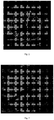
- a suitable diffraction pattern shown in Fig. 1 (an image for electron energy of 156 eV), constitutes a parameter indicating the presence on the surface of graphene. In accordance with the invention, it is a diffraction pattern typical for the graphene on the SiC surface (0001).
- the gray vector is a vector connected with the substrate's surface (silicon carbide), while the white vector is a vector connected with the graphene being synthesised.
- Diffraction maxima connected with silicon carbide are located in the corners of the gray hexagon, while the maxima connected with graphene are located in the corners of the white hexagon.
- the most intense diffraction maxima originating from silicon carbide are surrounded by six maxima of a lower intensity (the hexagon around the most bright peaks), while the most intense diffraction maxima originating from graphene are surrounded by two strongest maxima located towards the centre of the diffraction image (the maximum connected with graphene and two secondary maxima form a triangle). Additional maxima, also forming a hexagon but not always visible, may be located around the maximum connected with graphene.
- a parameter which allows for evaluating the quality and the crystallographic order is constituted by a ratio of intensities of the diffraction maxima to the background level.
- a signal analysis should be carried out between the two consecutive diffraction maxima connected with graphene, as shown for example in Fig. 2 .
- the signal intensity profile along this line is shown in Fig. 3 .
- the starting surface of silicon carbide (which is subjected to the graphitisation process thereafter) by annealing under ultra-high vacuum at temperatures from 100oC to 850oC, and annealing under a vacuum higher then 5 ⁇ 10 -5 Pa at a temperature from 900oC to 1050oC, combined with directing a stream of silicon atoms onto the sample, resulting in a nominal silicon growth rate of 0.5-2.5 ⁇ 10 -10 m/min.
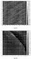
- the starting surface should be cooled to room temperature and its quality should be checked by diffraction methods (LEED). After the preparation, the surface is characterised by a (3 ⁇ 3) surface reconstruction, which is shown in the examples (A) below.
- the starting surface prepared by annealing in a stream of silicon atoms is characterised by a surface reconstruction of (3 ⁇ 3) type. Also, this surface is characterised by an almost perfect crystallographic ordering, which is proved by a very high number of observable diffraction maxima, their small transverse size, their high brightness and a low brightness of the background (a high ratio of the signal intensity to the background intensity, which proves a low number of crystallographic defects and amorphous areas of the surface).
- the surface prepared under vacuum is characterised by a reconstruction of (1 ⁇ 1) type and a low degree of crystallographic ordering, which is proved by a very high intensity of the background, a relatively low intensity of the diffraction maxima and a diffused transverse shape of the maxima.
- the starting surface prepared in a way described above was subjected to the graphitisation process at temperatures from 1300 to 1800oC in a stream of silicon atoms from an external sublimation source, corresponding to a nominal growth rate of silicon layers of 0.5-10 ⁇ 10 -10 m/min. under a pressure in the vacuum chamber not exceeding 5 ⁇ 10 -5 Pa.
- high-quality graphene (described in detail above) forms on the surface, which is shown in the examples (B) below:
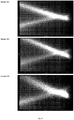
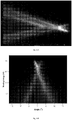
- Fig. 6 show the electron distribution in graphene in the vicinity of point K.
- the dispersion relation (dependence of energy on electron quasi-momentum, linearly proportional to the emission angle of the electron from the sample - vertical axis) should be linear around this point, which is evident for all samples, thus graphene has been formed on the surface of all samples.
- a parameter which allows for determining the impact of the surface ordering on the photoemission spectra is constituted by the background intensity.
- the lowest background intensity (formally the ratio of the signal intensity to the background intensity) was observed for sample B4 (the signal intensity between two branches of the linear dispersion relation is noteworthy).
- High-quality graphene may be obtained by the method according to the invention for relatively broad range of values of the critical parameters, particularly the graphitisation temperature and the stream of silicon atoms. It was illustrated in the preferred embodiments described below, which should not be however identified with the full scope of the invention being claimed.
- high quality graphene was formed on the surface of the sample, which was confirmed by diffraction and spectroscopic tests.
- the exact structure of the surface varies, but all of them are characterised by a very high crystallographic ordering and electron structures of high quality.
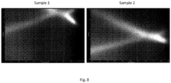
- the sample 4 is characterised by a very high quality of the surface, which is evidenced by sharp bands in the dispersion relation and a very low background level. Additionally, two graphene layers occur on the sample, which is evident in the ARPES spectrum as a splitting of linear branches of the dispersion relation. This fact confirms that the method according to the invention allows for controlling the number of the graphene layers formed on the surface.
- the graphene sample obtained in Example 4 was analysed by scanning tunnelling microscopy at room temperature under vacuum (an Omicron RT-STM/AFM microscope, the microscope tip made of etched tungsten, polarisation voltage of 15 mV, tunnelling current of 100 pA). The results in the form of a microscopic image are shown in Fig. 10A and B
- the perfect crystallographic structure of graphene is evident: the honeycomb structure.
- the unit cell of graphene is a single small hexagon; the change in the background intensity results from the effect of the subsurface layer (a buffer layer with a (6 ⁇ 3 ⁇ 6 ⁇ 3)R30o symmetry).
- the structure is characterised by a very low amount of any impurities or defects, confirming the high quality and crystallographic ordering on the surface of sample.
- the graphitisation process of the silicon carbide surface is carried out in a vacuum chamber ensuring a baseline pressure of the order of 1.3 ⁇ 10 -4 Pa (see Fig. 1A in the cited document).
- the described method suffers from the same significant purity limitation as the method described in the Patent No. US 9150417 B2 , in which the sublimation rate of silicon atoms is reduced by an application of buffer gases.
- the baseline pressure of the order of 1.3 ⁇ 10 -3 -1.3 ⁇ 10 -4 Pa corresponds to an exposure of the surface to unknown impurities of the order of 1 -10 L/s even before the beginning of annealing.
- the method according to the invention yields results different from the point of view of quality, thanks to application of a baseline pressure on the level of ultra-high vacuum, or approx. 1 ⁇ 10 -8 Pa (an exposure of the order of 0.0001 L/s), as well as maintaining the pressure in the chamber during the annealing at a level better than 5 ⁇ 10 -5 Pa (an exposure of the order of 0.5 L/s, or two orders of magnitude lower than in the method known from US 20110223094 A1 ).
- the method according to the invention allows for precise controlling of the value of the stream of silicon atoms and its change depending on the annealing temperature and time for the silicon carbide crystal. Thanks to precise control over the process parameters, the obtained results are significantly different than those obtained by the methods known earlier.
- the state of art does not provide the preliminary preparation of the silicon carbide surface.
- a preparation of the starting surface of silicon carbide subjected to graphitisation is carried out by annealing it at temperatures of 100oC-850oC under ultra-high vacuum, followed by annealing it at a temperature of 900-1100oC in a stream of silicon atoms, corresponding to a nominal rate of silicon growth of 0.5-2.5 ⁇ 10 -10 m/min, under ultra-high vacuum, and then cooling the crystal to room temperature.
- the preliminary preparation results in removal of impurities from the surface of silicon carbide before commencing graphitisation, during which the impurities could diffuse to the interior of the crystal, as well as form structural defects in the graphene layer and also, it results in formation of a high crystallographic order ((3 ⁇ 3) reconstruction of the surface) and smoothing of step edges.
- the presented results confirm that the preliminary preparation of the surface affects the quality and the structure of the graphene obtained in the graphitisation process advantageously.
- the known method excludes a direct control over temperature of the silicon carbide surface.
- the method according to the invention executes such a control using an optical pyrometer directed onto the sample.
- a precise temperature control is very important for obtaining optimal and repeatable results.
Landscapes
- Chemical & Material Sciences (AREA)
- Organic Chemistry (AREA)
- Engineering & Computer Science (AREA)
- Materials Engineering (AREA)
- Crystallography & Structural Chemistry (AREA)
- Metallurgy (AREA)
- Inorganic Chemistry (AREA)
- Nanotechnology (AREA)
- Chemical Kinetics & Catalysis (AREA)
- Physics & Mathematics (AREA)
- Thermal Sciences (AREA)
- General Chemical & Material Sciences (AREA)
- Carbon And Carbon Compounds (AREA)
- Crystals, And After-Treatments Of Crystals (AREA)
Priority Applications (1)
| Application Number | Priority Date | Filing Date | Title |
|---|---|---|---|
| PL17761570T PL3478634T3 (pl) | 2016-07-02 | 2017-06-30 | Sposób syntezy wysokiej jakości grafenu na powierzchni węglika krzemu |
Applications Claiming Priority (2)
| Application Number | Priority Date | Filing Date | Title |
|---|---|---|---|
| PL417804A PL417804A1 (pl) | 2016-07-02 | 2016-07-02 | Metoda syntezy wysokiej jakości grafenu na powierzchni węglika krzemu |
| PCT/IB2017/053969 WO2018007918A1 (en) | 2016-07-02 | 2017-06-30 | Method for preparation of high-quality graphene on the surface of silicon carbide |
Publications (2)
| Publication Number | Publication Date |
|---|---|
| EP3478634A1 EP3478634A1 (en) | 2019-05-08 |
| EP3478634B1 true EP3478634B1 (en) | 2021-10-27 |
Family
ID=59772660
Family Applications (1)
| Application Number | Title | Priority Date | Filing Date |
|---|---|---|---|
| EP17761570.5A Active EP3478634B1 (en) | 2016-07-02 | 2017-06-30 | Method for preparation of high-quality graphene on the surface of silicon carbide |
Country Status (7)
| Country | Link |
|---|---|
| US (1) | US20190226115A1 (enExample) |
| EP (1) | EP3478634B1 (enExample) |
| JP (1) | JP2019524620A (enExample) |
| KR (1) | KR20190024909A (enExample) |
| ES (1) | ES2901235T3 (enExample) |
| PL (2) | PL417804A1 (enExample) |
| WO (1) | WO2018007918A1 (enExample) |
Families Citing this family (6)
| Publication number | Priority date | Publication date | Assignee | Title |
|---|---|---|---|---|
| PL241895B1 (pl) * | 2019-09-23 | 2022-12-19 | Univ Jagiellonski | Sposób otrzymywania powierzchniowego kompozytu węglikowo- grafenowego o kontrolowanej morfologii powierzchni |
| CN112919456B (zh) * | 2021-02-23 | 2023-09-22 | 南京大学 | 一种具有均一层厚的平整石墨烯生长方法及单层或双层石墨烯薄膜 |
| CN115206462B (zh) * | 2022-06-30 | 2026-03-13 | 哈尔滨工业大学 | 基于流动气体法模拟单晶碳化硅干氧热氧化工艺的方法 |
| CN115849352B (zh) * | 2023-02-27 | 2023-05-16 | 太原理工大学 | 一种高效制备叠层石墨烯的方法 |
| CN117303355B (zh) * | 2023-10-16 | 2026-01-13 | 浙江大学杭州国际科创中心 | 一种利用循环加热制备石墨烯的方法 |
| CN120174461B (zh) * | 2025-04-07 | 2025-11-18 | 山东大学 | 一种在碳化硅衬底上外延均匀石墨烯的方法 |
Family Cites Families (4)
| Publication number | Priority date | Publication date | Assignee | Title |
|---|---|---|---|---|
| US8142754B2 (en) * | 2010-03-12 | 2012-03-27 | The Regents Of The University Of California | Method for synthesis of high quality graphene |
| JP5644175B2 (ja) * | 2010-04-27 | 2014-12-24 | 和人 山内 | SiC基板へのグラフェン成膜方法 |
| CN103097283B (zh) | 2010-09-16 | 2014-12-10 | 格拉芬斯克公司 | 石墨烯生长工艺 |
| KR101984697B1 (ko) | 2012-12-21 | 2019-05-31 | 삼성전자주식회사 | 그래핀 구조체, 이를 포함한 그래핀 소자 및 그 제조 방법 |
-
2016
- 2016-07-02 PL PL417804A patent/PL417804A1/pl unknown
-
2017
- 2017-06-30 US US16/314,313 patent/US20190226115A1/en not_active Abandoned
- 2017-06-30 KR KR1020187037935A patent/KR20190024909A/ko not_active Ceased
- 2017-06-30 ES ES17761570T patent/ES2901235T3/es active Active
- 2017-06-30 EP EP17761570.5A patent/EP3478634B1/en active Active
- 2017-06-30 PL PL17761570T patent/PL3478634T3/pl unknown
- 2017-06-30 WO PCT/IB2017/053969 patent/WO2018007918A1/en not_active Ceased
- 2017-06-30 JP JP2018569161A patent/JP2019524620A/ja active Pending
Non-Patent Citations (1)
| Title |
|---|
| None * |
Also Published As
| Publication number | Publication date |
|---|---|
| JP2019524620A (ja) | 2019-09-05 |
| PL417804A1 (pl) | 2018-01-15 |
| US20190226115A1 (en) | 2019-07-25 |
| ES2901235T3 (es) | 2022-03-21 |
| WO2018007918A1 (en) | 2018-01-11 |
| PL3478634T3 (pl) | 2022-04-11 |
| EP3478634A1 (en) | 2019-05-08 |
| KR20190024909A (ko) | 2019-03-08 |
Similar Documents
| Publication | Publication Date | Title |
|---|---|---|
| EP3478634B1 (en) | Method for preparation of high-quality graphene on the surface of silicon carbide | |
| Page et al. | Rotationally aligned hexagonal boron nitride on sapphire by high-temperature molecular beam epitaxy | |
| EP2738139B1 (en) | Polycrystalline diamond and manufacturing method therefor | |
| US10072355B2 (en) | Methods of forming graphene single crystal domains on a low nucleation site density substrate | |
| Chikvaidze et al. | Investigation of silicon carbide polytypes by Raman spectroscopy | |
| Gutierrez et al. | Multi-layer graphene obtained by high temperature carbon implantation into nickel films | |
| Delachat et al. | Properties of silicon nanoparticles embedded in SiN x deposited by microwave-PECVD | |
| Prevost et al. | Heteroepitaxial growth of sp2-hybridized boron nitride multilayer on nickel substrates by CVD: the key role of the substrate orientation | |
| Shestopalov et al. | Annealing, design and long-term operation of graphite crucibles for the growth of epitaxial graphene on SiC | |
| Hu et al. | Wafer‐Scale Synthesis of Monolayer Transition Metal Dichalcogenides Single Crystals via Designed “Trojan” Metal Precursor Supply Route | |
| Chen et al. | Microstructural and optical properties of high-quality ZnO epitaxially grown on a LiGaO 2 substrate | |
| Reidy et al. | Kinetic control for planar oxidation of MoS $ _2$ | |
| Baribeau et al. | Low-temperature Si growth on Si (001): Impurity incorporation and limiting thickness for epitaxy | |
| Kwon et al. | Synthesis of vertical arrays of ultra long ZnO nanowires on noncrystalline substrates | |
| Hwang et al. | Electron-beam assisted growth of hexagonal boron-nitride layer | |
| US9994971B2 (en) | Method for fabricating carbon-based composite material | |
| Kakanakova-Georgieva et al. | Sublimation epitaxy of AlN on SiC: growth morphology and structural features | |
| Vasin et al. | Study of the processes of carbonization and oxidation of porous silicon by Raman and IR spectroscopy | |
| Zhu et al. | Zinc oxide nanorods grown by arc discharge | |
| Khare et al. | Ion beam sputter deposition of epitaxial Ag films on native oxide covered Si (1 0 0) substrates | |
| Feria et al. | Few-layer large area graphene samples grown by CVD aiming application in electrochemical sensing devices | |
| Loginov et al. | Formation and properties of mesoporous MoS2 films | |
| Hilbrunner | Epitaxy of 2D Materials on Gallium Nitride | |
| Vodopyanov et al. | Indium Nitride Film Growth by Metal Organic Chemical Vapor Deposition with Nitrogen Activation in Electron Cyclotron Resonance Discharge Sustained by 24 GHz Gyrotron Radiation | |
| Byun et al. | Reduction of defects in GaN on reactive ion beam treated sapphire by annealing |
Legal Events
| Date | Code | Title | Description |
|---|---|---|---|
| STAA | Information on the status of an ep patent application or granted ep patent |
Free format text: STATUS: UNKNOWN |
|
| STAA | Information on the status of an ep patent application or granted ep patent |
Free format text: STATUS: THE INTERNATIONAL PUBLICATION HAS BEEN MADE |
|
| PUAI | Public reference made under article 153(3) epc to a published international application that has entered the european phase |
Free format text: ORIGINAL CODE: 0009012 |
|
| STAA | Information on the status of an ep patent application or granted ep patent |
Free format text: STATUS: REQUEST FOR EXAMINATION WAS MADE |
|
| 17P | Request for examination filed |
Effective date: 20190201 |
|
| AK | Designated contracting states |
Kind code of ref document: A1 Designated state(s): AL AT BE BG CH CY CZ DE DK EE ES FI FR GB GR HR HU IE IS IT LI LT LU LV MC MK MT NL NO PL PT RO RS SE SI SK SM TR |
|
| AX | Request for extension of the european patent |
Extension state: BA ME |
|
| DAV | Request for validation of the european patent (deleted) | ||
| DAX | Request for extension of the european patent (deleted) | ||
| STAA | Information on the status of an ep patent application or granted ep patent |
Free format text: STATUS: EXAMINATION IS IN PROGRESS |
|
| 17Q | First examination report despatched |
Effective date: 20191015 |
|
| RIC1 | Information provided on ipc code assigned before grant |
Ipc: B82Y 40/00 20110101ALI20210408BHEP Ipc: B82Y 30/00 20110101ALI20210408BHEP Ipc: C30B 33/02 20060101ALI20210408BHEP Ipc: C30B 29/02 20060101ALI20210408BHEP Ipc: C01B 32/188 20170101ALI20210408BHEP Ipc: C01B 32/184 20170101AFI20210408BHEP |
|
| GRAP | Despatch of communication of intention to grant a patent |
Free format text: ORIGINAL CODE: EPIDOSNIGR1 |
|
| STAA | Information on the status of an ep patent application or granted ep patent |
Free format text: STATUS: GRANT OF PATENT IS INTENDED |
|
| INTG | Intention to grant announced |
Effective date: 20210521 |
|
| GRAS | Grant fee paid |
Free format text: ORIGINAL CODE: EPIDOSNIGR3 |
|
| GRAA | (expected) grant |
Free format text: ORIGINAL CODE: 0009210 |
|
| STAA | Information on the status of an ep patent application or granted ep patent |
Free format text: STATUS: THE PATENT HAS BEEN GRANTED |
|
| AK | Designated contracting states |
Kind code of ref document: B1 Designated state(s): AL AT BE BG CH CY CZ DE DK EE ES FI FR GB GR HR HU IE IS IT LI LT LU LV MC MK MT NL NO PL PT RO RS SE SI SK SM TR |
|
| REG | Reference to a national code |
Ref country code: GB Ref legal event code: FG4D |
|
| REG | Reference to a national code |
Ref country code: CH Ref legal event code: EP |
|
| REG | Reference to a national code |
Ref country code: DE Ref legal event code: R096 Ref document number: 602017048303 Country of ref document: DE |
|
| REG | Reference to a national code |
Ref country code: AT Ref legal event code: REF Ref document number: 1441640 Country of ref document: AT Kind code of ref document: T Effective date: 20211115 |
|
| REG | Reference to a national code |
Ref country code: IE Ref legal event code: FG4D |
|
| REG | Reference to a national code |
Ref country code: SE Ref legal event code: TRGR |
|
| REG | Reference to a national code |
Ref country code: NL Ref legal event code: FP |
|
| PGFP | Annual fee paid to national office [announced via postgrant information from national office to epo] |
Ref country code: LU Payment date: 20211214 Year of fee payment: 6 |
|
| REG | Reference to a national code |
Ref country code: LT Ref legal event code: MG9D |
|
| REG | Reference to a national code |
Ref country code: AT Ref legal event code: MK05 Ref document number: 1441640 Country of ref document: AT Kind code of ref document: T Effective date: 20211027 |
|
| REG | Reference to a national code |
Ref country code: ES Ref legal event code: FG2A Ref document number: 2901235 Country of ref document: ES Kind code of ref document: T3 Effective date: 20220321 |
|
| PG25 | Lapsed in a contracting state [announced via postgrant information from national office to epo] |
Ref country code: RS Free format text: LAPSE BECAUSE OF FAILURE TO SUBMIT A TRANSLATION OF THE DESCRIPTION OR TO PAY THE FEE WITHIN THE PRESCRIBED TIME-LIMIT Effective date: 20211027 Ref country code: LT Free format text: LAPSE BECAUSE OF FAILURE TO SUBMIT A TRANSLATION OF THE DESCRIPTION OR TO PAY THE FEE WITHIN THE PRESCRIBED TIME-LIMIT Effective date: 20211027 Ref country code: FI Free format text: LAPSE BECAUSE OF FAILURE TO SUBMIT A TRANSLATION OF THE DESCRIPTION OR TO PAY THE FEE WITHIN THE PRESCRIBED TIME-LIMIT Effective date: 20211027 Ref country code: BG Free format text: LAPSE BECAUSE OF FAILURE TO SUBMIT A TRANSLATION OF THE DESCRIPTION OR TO PAY THE FEE WITHIN THE PRESCRIBED TIME-LIMIT Effective date: 20220127 Ref country code: AT Free format text: LAPSE BECAUSE OF FAILURE TO SUBMIT A TRANSLATION OF THE DESCRIPTION OR TO PAY THE FEE WITHIN THE PRESCRIBED TIME-LIMIT Effective date: 20211027 |
|
| PG25 | Lapsed in a contracting state [announced via postgrant information from national office to epo] |
Ref country code: IS Free format text: LAPSE BECAUSE OF FAILURE TO SUBMIT A TRANSLATION OF THE DESCRIPTION OR TO PAY THE FEE WITHIN THE PRESCRIBED TIME-LIMIT Effective date: 20220227 Ref country code: PT Free format text: LAPSE BECAUSE OF FAILURE TO SUBMIT A TRANSLATION OF THE DESCRIPTION OR TO PAY THE FEE WITHIN THE PRESCRIBED TIME-LIMIT Effective date: 20220228 Ref country code: NO Free format text: LAPSE BECAUSE OF FAILURE TO SUBMIT A TRANSLATION OF THE DESCRIPTION OR TO PAY THE FEE WITHIN THE PRESCRIBED TIME-LIMIT Effective date: 20220127 Ref country code: LV Free format text: LAPSE BECAUSE OF FAILURE TO SUBMIT A TRANSLATION OF THE DESCRIPTION OR TO PAY THE FEE WITHIN THE PRESCRIBED TIME-LIMIT Effective date: 20211027 Ref country code: HR Free format text: LAPSE BECAUSE OF FAILURE TO SUBMIT A TRANSLATION OF THE DESCRIPTION OR TO PAY THE FEE WITHIN THE PRESCRIBED TIME-LIMIT Effective date: 20211027 Ref country code: GR Free format text: LAPSE BECAUSE OF FAILURE TO SUBMIT A TRANSLATION OF THE DESCRIPTION OR TO PAY THE FEE WITHIN THE PRESCRIBED TIME-LIMIT Effective date: 20220128 |
|
| REG | Reference to a national code |
Ref country code: DE Ref legal event code: R097 Ref document number: 602017048303 Country of ref document: DE |
|
| PG25 | Lapsed in a contracting state [announced via postgrant information from national office to epo] |
Ref country code: SM Free format text: LAPSE BECAUSE OF FAILURE TO SUBMIT A TRANSLATION OF THE DESCRIPTION OR TO PAY THE FEE WITHIN THE PRESCRIBED TIME-LIMIT Effective date: 20211027 Ref country code: SK Free format text: LAPSE BECAUSE OF FAILURE TO SUBMIT A TRANSLATION OF THE DESCRIPTION OR TO PAY THE FEE WITHIN THE PRESCRIBED TIME-LIMIT Effective date: 20211027 Ref country code: RO Free format text: LAPSE BECAUSE OF FAILURE TO SUBMIT A TRANSLATION OF THE DESCRIPTION OR TO PAY THE FEE WITHIN THE PRESCRIBED TIME-LIMIT Effective date: 20211027 Ref country code: EE Free format text: LAPSE BECAUSE OF FAILURE TO SUBMIT A TRANSLATION OF THE DESCRIPTION OR TO PAY THE FEE WITHIN THE PRESCRIBED TIME-LIMIT Effective date: 20211027 Ref country code: DK Free format text: LAPSE BECAUSE OF FAILURE TO SUBMIT A TRANSLATION OF THE DESCRIPTION OR TO PAY THE FEE WITHIN THE PRESCRIBED TIME-LIMIT Effective date: 20211027 Ref country code: CZ Free format text: LAPSE BECAUSE OF FAILURE TO SUBMIT A TRANSLATION OF THE DESCRIPTION OR TO PAY THE FEE WITHIN THE PRESCRIBED TIME-LIMIT Effective date: 20211027 |
|
| PGFP | Annual fee paid to national office [announced via postgrant information from national office to epo] |
Ref country code: SE Payment date: 20220609 Year of fee payment: 6 Ref country code: GB Payment date: 20220608 Year of fee payment: 6 |
|
| PGFP | Annual fee paid to national office [announced via postgrant information from national office to epo] |
Ref country code: PL Payment date: 20220610 Year of fee payment: 6 |
|
| PLBE | No opposition filed within time limit |
Free format text: ORIGINAL CODE: 0009261 |
|
| STAA | Information on the status of an ep patent application or granted ep patent |
Free format text: STATUS: NO OPPOSITION FILED WITHIN TIME LIMIT |
|
| 26N | No opposition filed |
Effective date: 20220728 |
|
| PG25 | Lapsed in a contracting state [announced via postgrant information from national office to epo] |
Ref country code: AL Free format text: LAPSE BECAUSE OF FAILURE TO SUBMIT A TRANSLATION OF THE DESCRIPTION OR TO PAY THE FEE WITHIN THE PRESCRIBED TIME-LIMIT Effective date: 20211027 |
|
| PG25 | Lapsed in a contracting state [announced via postgrant information from national office to epo] |
Ref country code: SI Free format text: LAPSE BECAUSE OF FAILURE TO SUBMIT A TRANSLATION OF THE DESCRIPTION OR TO PAY THE FEE WITHIN THE PRESCRIBED TIME-LIMIT Effective date: 20211027 |
|
| PG25 | Lapsed in a contracting state [announced via postgrant information from national office to epo] |
Ref country code: MC Free format text: LAPSE BECAUSE OF FAILURE TO SUBMIT A TRANSLATION OF THE DESCRIPTION OR TO PAY THE FEE WITHIN THE PRESCRIBED TIME-LIMIT Effective date: 20211027 |
|
| REG | Reference to a national code |
Ref country code: CH Ref legal event code: PL |
|
| REG | Reference to a national code |
Ref country code: NL Ref legal event code: MM Effective date: 20220701 |
|
| REG | Reference to a national code |
Ref country code: BE Ref legal event code: MM Effective date: 20220630 |
|
| PG25 | Lapsed in a contracting state [announced via postgrant information from national office to epo] |
Ref country code: NL Free format text: LAPSE BECAUSE OF NON-PAYMENT OF DUE FEES Effective date: 20220701 |
|
| PG25 | Lapsed in a contracting state [announced via postgrant information from national office to epo] |
Ref country code: CH Free format text: LAPSE BECAUSE OF NON-PAYMENT OF DUE FEES Effective date: 20220630 Ref country code: LI Free format text: LAPSE BECAUSE OF NON-PAYMENT OF DUE FEES Effective date: 20220630 Ref country code: IE Free format text: LAPSE BECAUSE OF NON-PAYMENT OF DUE FEES Effective date: 20220630 |
|
| PG25 | Lapsed in a contracting state [announced via postgrant information from national office to epo] |
Ref country code: IT Free format text: LAPSE BECAUSE OF FAILURE TO SUBMIT A TRANSLATION OF THE DESCRIPTION OR TO PAY THE FEE WITHIN THE PRESCRIBED TIME-LIMIT Effective date: 20211027 Ref country code: BE Free format text: LAPSE BECAUSE OF NON-PAYMENT OF DUE FEES Effective date: 20220630 |
|
| P01 | Opt-out of the competence of the unified patent court (upc) registered |
Effective date: 20230720 |
|
| GBPC | Gb: european patent ceased through non-payment of renewal fee |
Effective date: 20230630 |
|
| PG25 | Lapsed in a contracting state [announced via postgrant information from national office to epo] |
Ref country code: LU Free format text: LAPSE BECAUSE OF NON-PAYMENT OF DUE FEES Effective date: 20230630 |
|
| REG | Reference to a national code |
Ref country code: SE Ref legal event code: EUG |
|
| PG25 | Lapsed in a contracting state [announced via postgrant information from national office to epo] |
Ref country code: LU Free format text: LAPSE BECAUSE OF NON-PAYMENT OF DUE FEES Effective date: 20230630 Ref country code: HU Free format text: LAPSE BECAUSE OF FAILURE TO SUBMIT A TRANSLATION OF THE DESCRIPTION OR TO PAY THE FEE WITHIN THE PRESCRIBED TIME-LIMIT; INVALID AB INITIO Effective date: 20170630 |
|
| PG25 | Lapsed in a contracting state [announced via postgrant information from national office to epo] |
Ref country code: MK Free format text: LAPSE BECAUSE OF FAILURE TO SUBMIT A TRANSLATION OF THE DESCRIPTION OR TO PAY THE FEE WITHIN THE PRESCRIBED TIME-LIMIT Effective date: 20211027 Ref country code: CY Free format text: LAPSE BECAUSE OF FAILURE TO SUBMIT A TRANSLATION OF THE DESCRIPTION OR TO PAY THE FEE WITHIN THE PRESCRIBED TIME-LIMIT Effective date: 20211027 Ref country code: GB Free format text: LAPSE BECAUSE OF NON-PAYMENT OF DUE FEES Effective date: 20230630 |
|
| PG25 | Lapsed in a contracting state [announced via postgrant information from national office to epo] |
Ref country code: SE Free format text: LAPSE BECAUSE OF NON-PAYMENT OF DUE FEES Effective date: 20230701 |
|
| PG25 | Lapsed in a contracting state [announced via postgrant information from national office to epo] |
Ref country code: TR Free format text: LAPSE BECAUSE OF FAILURE TO SUBMIT A TRANSLATION OF THE DESCRIPTION OR TO PAY THE FEE WITHIN THE PRESCRIBED TIME-LIMIT Effective date: 20211027 |
|
| PG25 | Lapsed in a contracting state [announced via postgrant information from national office to epo] |
Ref country code: MT Free format text: LAPSE BECAUSE OF FAILURE TO SUBMIT A TRANSLATION OF THE DESCRIPTION OR TO PAY THE FEE WITHIN THE PRESCRIBED TIME-LIMIT Effective date: 20211027 |
|
| PG25 | Lapsed in a contracting state [announced via postgrant information from national office to epo] |
Ref country code: PL Free format text: LAPSE BECAUSE OF NON-PAYMENT OF DUE FEES Effective date: 20230630 |
|
| PG25 | Lapsed in a contracting state [announced via postgrant information from national office to epo] |
Ref country code: PL Free format text: LAPSE BECAUSE OF NON-PAYMENT OF DUE FEES Effective date: 20230630 |
|
| PGFP | Annual fee paid to national office [announced via postgrant information from national office to epo] |
Ref country code: DE Payment date: 20250620 Year of fee payment: 9 |
|
| PGFP | Annual fee paid to national office [announced via postgrant information from national office to epo] |
Ref country code: FR Payment date: 20250612 Year of fee payment: 9 |
|
| PGFP | Annual fee paid to national office [announced via postgrant information from national office to epo] |
Ref country code: ES Payment date: 20250718 Year of fee payment: 9 |