EP3477704A1 - Camera photosensitive component, camera, and camera shooting terminal - Google Patents
Camera photosensitive component, camera, and camera shooting terminal Download PDFInfo
- Publication number
- EP3477704A1 EP3477704A1 EP18201616.2A EP18201616A EP3477704A1 EP 3477704 A1 EP3477704 A1 EP 3477704A1 EP 18201616 A EP18201616 A EP 18201616A EP 3477704 A1 EP3477704 A1 EP 3477704A1
- Authority
- EP
- European Patent Office
- Prior art keywords
- microprism
- pixel
- color lights
- emitted
- subpixels
- Prior art date
- Legal status (The legal status is an assumption and is not a legal conclusion. Google has not performed a legal analysis and makes no representation as to the accuracy of the status listed.)
- Granted
Links
Images



Classifications
-
- G—PHYSICS
- G03—PHOTOGRAPHY; CINEMATOGRAPHY; ANALOGOUS TECHNIQUES USING WAVES OTHER THAN OPTICAL WAVES; ELECTROGRAPHY; HOLOGRAPHY
- G03B—APPARATUS OR ARRANGEMENTS FOR TAKING PHOTOGRAPHS OR FOR PROJECTING OR VIEWING THEM; APPARATUS OR ARRANGEMENTS EMPLOYING ANALOGOUS TECHNIQUES USING WAVES OTHER THAN OPTICAL WAVES; ACCESSORIES THEREFOR
- G03B1/00—Film strip handling
-
- H—ELECTRICITY
- H10—SEMICONDUCTOR DEVICES; ELECTRIC SOLID-STATE DEVICES NOT OTHERWISE PROVIDED FOR
- H10F—INORGANIC SEMICONDUCTOR DEVICES SENSITIVE TO INFRARED RADIATION, LIGHT, ELECTROMAGNETIC RADIATION OF SHORTER WAVELENGTH OR CORPUSCULAR RADIATION
- H10F39/00—Integrated devices, or assemblies of multiple devices, comprising at least one element covered by group H10F30/00, e.g. radiation detectors comprising photodiode arrays
- H10F39/80—Constructional details of image sensors
- H10F39/806—Optical elements or arrangements associated with the image sensors
- H10F39/8063—Microlenses
-
- H—ELECTRICITY
- H10—SEMICONDUCTOR DEVICES; ELECTRIC SOLID-STATE DEVICES NOT OTHERWISE PROVIDED FOR
- H10F—INORGANIC SEMICONDUCTOR DEVICES SENSITIVE TO INFRARED RADIATION, LIGHT, ELECTROMAGNETIC RADIATION OF SHORTER WAVELENGTH OR CORPUSCULAR RADIATION
- H10F39/00—Integrated devices, or assemblies of multiple devices, comprising at least one element covered by group H10F30/00, e.g. radiation detectors comprising photodiode arrays
- H10F39/80—Constructional details of image sensors
- H10F39/806—Optical elements or arrangements associated with the image sensors
-
- H—ELECTRICITY
- H04—ELECTRIC COMMUNICATION TECHNIQUE
- H04N—PICTORIAL COMMUNICATION, e.g. TELEVISION
- H04N23/00—Cameras or camera modules comprising electronic image sensors; Control thereof
-
- H—ELECTRICITY
- H10—SEMICONDUCTOR DEVICES; ELECTRIC SOLID-STATE DEVICES NOT OTHERWISE PROVIDED FOR
- H10F—INORGANIC SEMICONDUCTOR DEVICES SENSITIVE TO INFRARED RADIATION, LIGHT, ELECTROMAGNETIC RADIATION OF SHORTER WAVELENGTH OR CORPUSCULAR RADIATION
- H10F39/00—Integrated devices, or assemblies of multiple devices, comprising at least one element covered by group H10F30/00, e.g. radiation detectors comprising photodiode arrays
- H10F39/10—Integrated devices
- H10F39/12—Image sensors
- H10F39/18—Complementary metal-oxide-semiconductor [CMOS] image sensors; Photodiode array image sensors
- H10F39/182—Colour image sensors
-
- H—ELECTRICITY
- H10—SEMICONDUCTOR DEVICES; ELECTRIC SOLID-STATE DEVICES NOT OTHERWISE PROVIDED FOR
- H10F—INORGANIC SEMICONDUCTOR DEVICES SENSITIVE TO INFRARED RADIATION, LIGHT, ELECTROMAGNETIC RADIATION OF SHORTER WAVELENGTH OR CORPUSCULAR RADIATION
- H10F39/00—Integrated devices, or assemblies of multiple devices, comprising at least one element covered by group H10F30/00, e.g. radiation detectors comprising photodiode arrays
- H10F39/80—Constructional details of image sensors
- H10F39/802—Geometry or disposition of elements in pixels, e.g. address-lines or gate electrodes
-
- H—ELECTRICITY
- H10—SEMICONDUCTOR DEVICES; ELECTRIC SOLID-STATE DEVICES NOT OTHERWISE PROVIDED FOR
- H10F—INORGANIC SEMICONDUCTOR DEVICES SENSITIVE TO INFRARED RADIATION, LIGHT, ELECTROMAGNETIC RADIATION OF SHORTER WAVELENGTH OR CORPUSCULAR RADIATION
- H10F39/00—Integrated devices, or assemblies of multiple devices, comprising at least one element covered by group H10F30/00, e.g. radiation detectors comprising photodiode arrays
- H10F39/80—Constructional details of image sensors
- H10F39/805—Coatings
- H10F39/8053—Colour filters
Definitions
- the present disclosure generally relates to the technical field of camera shooting, and more particularly, to a camera photosensitive component, a camera, and a camera shooting terminal.
- a camera photosensitive component includes a Red, Green and Blue (RGB) filter, and light is emitted onto a photosensitive surface of a pixel after being filtered through the RGB filter.
- RGB Red, Green and Blue
- the present disclosure provides a camera photosensitive component, a camera, and a camera shooting terminal in accordance with claims which follow.
- a camera photosensitive component which may include: a silicon substrate layer, a pixel array layer attached to one surface of the silicon substrate layer and a microprism layer arranged in parallel with the pixel array layer, wherein microprisms in the microprism layer may be configured to decompose incident light into m color lights for emission, and n color lights in the emitted m color lights are respectively emitted into subpixels in corresponding colors of pixels corresponding to the microprisms, and n is not greater than m.
- each microprism may correspond to a pixel, and the pixel may include n subpixels.
- the microprism may be configured to decompose the incident light into the m color lights for emission, and the n color lights in the emitted m color lights may be emitted into the subpixels in the corresponding colors of the pixel.
- a bottom surface of the microprism may be perpendicular to a plane where the pixel array layer is located, and the n subpixels arranged in ascending order of refractive indexes of the corresponding colors may be sequentially arranged in the pixel along a direction from a vertex of the microprism to the bottom surface.
- every two adjacent microprisms may correspond to two adjacent pixels, wherein each of the first pixel and the second pixel may include n subpixels, and the nth subpixels in the first pixel and the second pixel may be adjacent.
- the first microprism may be configured to decompose the incident light into the m color lights for emission, the n color lights in the emitted m color lights may be respectively emitted into the subpixels in the corresponding colors of the first pixel, the second microprism may be configured to decompose the incident light into the m color lights for emission, and the n color lights in the emitted m color lights may be respectively emitted into the subpixels in the corresponding colors of the second pixel.
- a bottom surface of the first microprism may be opposite and parallel to a bottom surface of the second microprism, the bottom surface of the first microprism may be perpendicular to the plane where the pixel array layer is located, and the bottom surface of the second microprism may be perpendicular to the plane where the pixel array layer is located.
- n subpixels arranged in ascending order of refractive indexes of the corresponding colors may be sequentially arranged in the first pixel along a direction from a vertex of the first microprism towards the bottom surface of the first microprism, and the n subpixels arranged in ascending order of refractive indexes of the corresponding colors may be sequentially arranged in the second pixel along a direction from a vertex of the second microprism towards the bottom surface of the second microprism.
- every two adjacent microprisms may correspond to two adjacent pixels, the first pixel and the second pixel may include totally 2n-1 subpixels, and the first pixel and the second pixel may share the nth subpixel.
- the first microprism may be configured to decompose the incident light into the m color lights for emission, the n color lights in the emitted m color lights may be respectively emitted into n-1 subpixels in the corresponding colors of the first pixel and the shared nth subpixel, the second microprism may be configured to decompose the incident light into the m color lights for emission, and the n color lights in the emitted m color lights may be respectively emitted into n-1 subpixels in the corresponding colors of the second pixel and the shared nth subpixel.
- a bottom surface of the first microprism may be opposite and parallel to a bottom surface of the second microprism, the bottom surface of the first microprism may be perpendicular to the plane where the pixel array layer is located, and the bottom surface of the second microprism may be perpendicular to the plane where the pixel array layer is located.
- n-1 subpixels arranged in ascending order of refractive indexes of the corresponding colors and the shared nth subpixel may be sequentially arranged in the first pixel along a direction from a vertex of the first microprism to the bottom surface
- the n-1 subpixels arranged in ascending order of refractive indexes of the corresponding colors and the shared nth subpixel may be sequentially arranged in the second pixel along a direction from a vertex of the second microprism to the bottom surface.
- the camera photosensitive component may further include a microlens layer located between the pixel array layer and the microprism layer.
- the microprisms may be configured to decompose the incident light into the m color lights for emission.
- Microlenses in the microlens layer may be configured to independently converge each type of color light of the n color lights in the m color lights emitted by the microprisms for respective emission into the subpixels in the corresponding colors of the pixels corresponding to the microprisms.
- the camera photosensitive component may further include a microlens layer, the microlens layer may be parallel to the microprism layer, and the microlens layer may be nonadjacent to the pixel array layer.
- Microlenses in the microlens layer may be configured to converge the incident light for emission.
- the microprisms may be configured to decompose the converged light emitted by the microlenses into the m color lights for emission, and the n color lights in the emitted m color lights may be emitted into the subpixels in the corresponding colors of the pixels corresponding to the microprisms.
- the microprism layer may include an array of microprisms.
- the microprism layer may be formed by etching a substrate made from a preset material.
- a camera which may include the camera photosensitive component of the first aspect.
- a camera shooting terminal which may include the camera of the second aspect.
- Fig. 1 is a structure diagram of a camera photosensitive component according to known technology.
- the camera photosensitive component includes a silicon substrate layer, a pixel array layer attached to one surface of the silicon substrate layer, an RGB filter layer arranged in parallel with the pixel array layer and a microlens layer arranged in parallel with the RGB filter layer, and the microlens layer is nonadjacent to the pixel array layer.
- a pixel may include three or four or even more subpixels. Descriptions will be made with the condition that a pixel includes three subpixels as an example. Then, the three subpixels are a red subpixel, a green subpixel and a blue subpixel respectively.
- an RGB filter includes three light filters, i.e. a red light filter, a green light filter and a blue light filter respectively. A microlens is arranged above each light filter.
- Incident light is perpendicularly emitted into each microlens in the microlens layer, and each microlens refracts the incident light into the corresponding light filter below.
- the red light filter absorbs light except red light, and emits the red light into the red subpixel;
- the green light filter absorbs light except green light, and emits the green light into the green subpixel;
- the blue light filter absorbs light except blue light, and emits the blue light into the blue subpixel.
- Transmittance of the incident light through the RGB filter is very low, averagely about 40%, and the other 60% of light is absorbed, so that an exposure time required by imaging is prolonged.
- the instant application solves the problem through aspects shown in Fig. 2 to Fig. 6 .
- Fig. 2 is a structure diagram of a camera photosensitive component, according to an exemplary aspect.
- the camera photosensitive component may be implemented as a camera, and the camera is applied to a camera shooting terminal.
- the camera photosensitive component includes: a silicon substrate layer 210, a pixel array layer 220 attached to one surface of the silicon substrate layer 210, and a microprism layer 230 arranged in parallel with the pixel array layer 220.
- the silicon substrate layer 210 may include a silicon material such as polysilicon.
- the pixel array layer 220 may include a plurality of pixels arranged in a predetermined number of columns and rows.
- the microprism layer 230 may include microprisms, where a microprism may be a precise small prism made of optical glass.
- Microprisms 231 in the microprism layer 230 are configured to decompose incident light into m color lights for emission, and n color lights in the emitted m color lights are respectively emitted into subpixels in corresponding colors of pixels corresponding to the microprisms 231.
- n is not greater than m.
- m may be 7, and may also be another numerical value, which will not be limited in the aspect.
- the microprisms 231 may decompose the incident light into seven types of color lights.
- a pixel may include three or four or even more subpixels. Descriptions will be made with the condition that a pixel includes three subpixels as an example. Then, each microprism 231 in the microprism layer 230 is configured to decompose the incident light into the seven color lights for emission, emitted red light is emitted into a red subpixel 221 of the pixel corresponding to the microprism 231, emitted green light is emitted into a green subpixel 222 of the pixel, and emitted blue light is emitted into a blue subpixel 223 of the pixel.
- the microprisms decompose the incident light into the m color lights for emission, and the n color lights in the emitted m color lights are respectively emitted into the subpixels in the corresponding colors of the pixels corresponding to the microprisms.
- the n color lights may be formed by decomposition with the microprisms, not obtained after part of color light is absorbed by an RGB filter, and transmittance of the color light emitted into the pixels may be improved, so that an exposure time required by imaging is reduced, a camera shooting effect under a low-lighting condition may further be improved, and the camera shooting effect on a moving object may also be improved.
- the camera photosensitive component includes: a silicon substrate layer 210, a pixel array layer 220 attached to one surface of the silicon substrate layer 210 and a microprism layer 230 arranged in parallel with the pixel array layer 220.
- the pixel array layer 220 includes a pixel array, and each pixel includes three or four or even more subpixels.
- the three subpixels may be a red subpixel, a green subpixel and a blue subpixel respectively.
- the four subpixels are a red subpixel, a green subpixel, a blue subpixel, and a yellow subpixel, respectively.
- the four subpixels are a red subpixel, a green subpixel, a blue subpixel, and a white subpixel, respectively.
- a number of subpixels included in each pixel and the subpixels are not limited in the aspect.
- Grooves are formed in the surface, attached to the pixel array layer 220, of the silicon substrate layer 210, and each subpixel in each pixel is located in a groove.
- Microprisms 231 in the microprism layer 230 are configured to decompose incident light into m color lights for emission, and n color lights in the emitted m color lights are emitted into subpixels in corresponding colors of pixels corresponding to the microprisms 231 respectively, n ⁇ m.
- m may be 7, and may also be another numerical value, which will not be limited in the aspect.
- the microprisms 231 may decompose the incident light into seven color lights.
- each microprism 231 in the microprism layer 230 is configured to decompose the incident light into the seven color lights for emission, emitted red light is emitted into a red subpixel 221 of the pixel corresponding to the microprism 231, emitted green light is emitted into a green subpixel 222 of the pixel, and emitted blue light is emitted into a blue subpixel 223 of the pixel.
- the microprism layer 230 is configured to decompose the incident light for emission into the pixels.
- the n color lights may be formed by decomposition with the microprisms 231, not obtained after part of color light is absorbed by an RGB filter, and transmittance of the color light emitted into the pixels may be improved, so that an exposure time required by imaging is reduced, a camera shooting effect under a low-lighting condition may further be improved, and the camera shooting effect on a moving object may also be improved.
- a pixel includes three subpixels as an example. Then, red light emitted by the microprism 231 is emitted into the red subpixel 221 of the pixel, emitted green light is emitted into the green subpixel 222 of the pixel, and emitted blue light is emitted into the blue subpixel 223 of the pixel.
- a bottom surface 232 of the microprism 231 is perpendicular to a plane where the pixel array layer 220 is located, and n subpixels arranged in ascending order of refractive indexes (i.e., from small to large refractive indexes) of the corresponding colors are sequentially arranged in the pixel along a direction from a vertex 233 of the microprism 231 to the bottom surface 232.
- a pixel includes three subpixels as an example. Since a refractive index of the red light is smallest and a refractive index of the blue light is largest, the red subpixel 221, the green subpixel 222 and the blue subpixel 223 are sequentially arranged in the pixel along the direction from the vertex 233 of the microprism 231 to the bottom surface 232.
- a pixel includes three subpixels as an example.
- the red light emitted by the first microprism 231 is emitted into the red subpixel 221 of the first pixel
- the emitted green light is emitted into the green subpixel 222 of the first pixel
- the emitted blue light is emitted into the blue subpixel 223 of the first pixel.
- the red light emitted by the second microprism 231 is emitted into the red subpixel 221 of the second pixel
- the emitted green light is emitted into the green subpixel 222 of the second pixel
- the emitted blue light is emitted into the blue subpixel 223 of the second pixel.
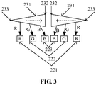
- a bottom surface 232 of the first microprism 231 is opposite and parallel to a bottom surface 232 of the second microprism 231, the bottom surface 232 of the first microprism 231 is perpendicular to the plane where the pixel array layer 220 is located, and the bottom surface 232 of the second microprism 231 is perpendicular to the plane where the pixel array layer 220 is located; and n subpixels arranged in ascending order of refractive indexes of the corresponding colors are sequentially arranged in the first pixel along a direction from a vertex 233 of the first microprism 231 to the bottom surface 232, and n subpixels arranged in ascending order of refractive indexes of the corresponding colors are sequentially arranged in the second pixel along a direction from a vertex 233 of the second microprism 231 to the bottom surface 232.
- the direction of the dotted arrow on the left side is the direction from the vertex 233 of the first microprism 231 towards the bottom surface 232
- the direction of the dotted arrow on the right side is the direction from the vertex 233 of the second microprism 231 towards the bottom surface 232.
- a pixel includes three subpixels as an example. Since the refractive index of the red light is smallest and the refractive index of the blue light is largest, the red subpixel 221, the green subpixel 222 and the blue subpixel 223 are sequentially arranged in the first pixel along the direction from the vertex 233 of the first microprism 231 to the bottom surface 232. Similarly, the red subpixel 221, the green subpixel 222 and the blue subpixel 223 are sequentially arranged in the second pixel along the direction from the vertex 233 of the second microprism 231 to the bottom surface 232. Further, the blue subpixel 223 in the first pixel is adjacent to the blue subpixel 223 in the second pixel.
- a pixel includes three subpixels as an example. Then, the red light emitted by the first microprism 231 is emitted into the red subpixel 221 of the first pixel, the emitted green light is emitted into the green subpixel 222 of the first pixel, and the emitted blue light is emitted into the shared blue subpixel 223; and the red light emitted by the second microprism 231 is emitted into the red subpixel 221 of the second pixel, the emitted green light is emitted into the green subpixel 222 of the second pixel, and the emitted blue light is emitted into the shared blue subpixel 223.
- the first pixels and the second pixels share the nth subpixels, and since the shared subpixels have relatively large areas, photosensitive areas of the subpixels may be enlarged. Therefore, light transmittance of the subpixels is improved, and the exposure time required by imaging is reduced.
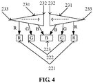
- a bottom surface 232 of the first microprism 231 is opposite and parallel to a bottom surface 232 of the second microprism 231, the bottom surface 232 of the first microprism 231 is perpendicular to the plane where the pixel array layer 220 is located, and the bottom surface 232 of the second microprism 231 is perpendicular to the plane where the pixel array layer is located; and n-1 subpixels arranged in ascending order of refractive indexes of the corresponding colors and the shared nth subpixel are sequentially arranged in the first pixel along a direction from a vertex 233 of the first microprism 231 to the bottom surface 232, and n-1 subpixels arranged in ascending order of refractive indexes of the corresponding colors and the shared nth subpixel are sequentially arranged in the second pixel along a direction from a vertex 233 of the second microprism 231 to the bottom surface 232.
- the direction of the dotted arrow on the left side is the direction from the vertex 233 of the first microprism 231 points towards the bottom surface 232
- the direction of the dotted arrow on the right side is the direction from the vertex 233 of the second microprism 231 points towards the bottom surface 232.
- a pixel includes three subpixels as an example. Since the refractive index of the red light is smallest and the refractive index of the blue light is largest, the red subpixel 221, the green subpixel 222 and the shared blue subpixel 223 are sequentially arranged in the first pixel along the direction from the vertex 233 of the first microprism 231 to the bottom surface 232, and the red subpixel 221, the green subpixel 222 and the shared blue subpixel 223 are sequentially arranged in the second pixel along the direction from the vertex 233 of the second microprism 231 to the bottom surface 232.
- a microlens layer 240 may further be arranged between the pixel array layer 220 and the microprism layer 230.
- the microlens layer 240 is configured to converge the light, and may not influence the transmittance of the light, wherein there may be multiple position relationships between the microlens layer 240 and the microprism layer 230. Descriptions will be made in the aspect with two of them as examples.
- each microlens 241 corresponds to a subpixel, referring to Fig. 6 . Descriptions will be made still with the condition that a pixel includes three subpixels as an example. Then, the microprism 231 decomposes the incident light converged by the microlens 241 into seven color lights for emission, the emitted red light is emitted into the red subpixel 221 of the pixel corresponding to the microprism 231, the emitted green light is emitted into the green subpixel 222 of the pixel, and the emitted blue light is emitted into the blue subpixel 223 of the pixel.
- microprism layer 230 There are multiple manners for manufacturing the microprism layer 230. Descriptions will be made in the aspect with two of them as examples.
- the microprisms decompose the incident light into the m color lights for emission, and the n color lights in the emitted m color lights are emitted into the subpixels in the corresponding colors of the pixels corresponding to the microprisms respectively.
- the n color lights may be formed by decomposition with the microprisms, not obtained after part of color light is absorbed by an RGB filter, and the transmittance of the color light emitted into the pixels may be improved, so that the exposure time required by imaging is reduced, the camera shooting effect under the low-lighting condition may further be improved, and the camera shooting effect on the moving object may also be improved.
- the first pixels and the second pixels share the nth subpixels. Accordingly, the shared subpixels have relatively large areas, and the photosensitive areas of the subpixels may be enlarged. Therefore, the light transmittance of the subpixels is improved, and the exposure time required by imaging is reduced.
- the microlens layer is located between the pixel array layer and the microprism layer, then the microlens layer may independently converge each type of color light of the n color lights emitted by the microprism layer for respective emission into the subpixels in the corresponding colors of the pixels corresponding to the microprisms, and complete emission of each color light into the subpixels in the corresponding colors may be ensured, so that the light transmittance of the subpixels is improved, and the exposure time required by imaging is reduced.
- the microprism layer is formed by etching the substrate made from the preset material, so that it is unnecessary to manufacture and arrange microprisms with same or approximately same sizes of the pixels, and difficulties in implementation of the microprism layer may be reduced.
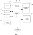
- Fig. 7 is a block diagram of a device 700 carrying a camera photosensitive component, according to an exemplary aspect.
- the device 700 may be a mobile phone, a computer, a digital broadcast terminal, a messaging device, a gaming console, a tablet, a medical device, exercise equipment, a personal digital assistant, and the like.
- the device 700 may include one or more of the following components: a processing component 702, a memory 704, a power component 706, a multimedia component 708, an audio component 710, an Input/Output (I/O) interface 712, a sensor component 714, and a communication component 716.
- a processing component 702 a memory 704
- a power component 706 a multimedia component 708, an audio component 710, an Input/Output (I/O) interface 712, a sensor component 714, and a communication component 716.
- I/O Input/Output
- the processing component 702 typically controls overall operations of the device 700, such as the operations associated with display, telephone calls, data communications, camera operations, and recording operations.
- the processing component 702 may include one or more processors 718 to execute instructions to perform all or part of the steps in the abovementioned method.
- the processing component 702 may include one or more modules which facilitate interaction between the processing component 702 and the other components.
- the processing component 702 may include a multimedia module to facilitate interaction between the multimedia component 708 and the processing component 702.
- the memory 704 is configured to store various types of data to support the operation of the device 700. Examples of such data include instructions for any application programs or methods operated on the device 700, contact data, phonebook data, messages, pictures, video, etc.
- the memory 704 may be implemented by any type of volatile or non-volatile memory devices, or a combination thereof, such as a Static Random Access Memory (SRAM), an Electrically Erasable Programmable Read-Only Memory (EEPROM), an Erasable Programmable Read-Only Memory (EPROM), a Programmable Read-Only Memory (PROM), a Read-Only Memory (ROM), a magnetic memory, a flash memory, and a magnetic or optical disk.
- SRAM Static Random Access Memory
- EEPROM Electrically Erasable Programmable Read-Only Memory
- EPROM Erasable Programmable Read-Only Memory
- PROM Programmable Read-Only Memory
- ROM Read-Only Memory
- magnetic memory a magnetic memory
- flash memory and a magnetic or optical disk.
- the power component 706 provides power for various components of the device 700.
- the power component 706 may include a power management system, one or more power supplies, and other components associated with the generation, management and distribution of power for the device 700.
- the multimedia component 708 includes a screen providing an output interface between the device 700 and a user.
- the screen may include a Liquid Crystal Display (LCD) and a Touch Panel (TP). If the screen includes the TP, the screen may be implemented as a touch screen to receive an input signal from the user.
- the TP includes one or more touch sensors to sense touches, swipes and gestures on the TP. The touch sensors may not only sense a boundary of a touch or swipe action, but also detect a duration and pressure associated with the touch or swipe action.
- the multimedia component 708 includes a front camera and/or a rear camera. The front camera and/or the rear camera may receive external multimedia data when the device 700 is in an operation mode, such as a photographing mode or a video mode. Each of the front camera and the rear camera may be a fixed optical lens system or have focusing and optical zooming capabilities.
- the audio component 710 is configured to output and/or input an audio signal.
- the audio component 710 includes a Microphone (MIC), and the MIC is configured to receive an external audio signal when the device 700 is in the operation mode, such as a call mode, a recording mode and a voice recognition mode.
- the received audio signal may be further stored in the memory 704 or sent through the communication component 716.
- the audio component 710 further includes a speaker configured to output the audio signal.
- the I/O interface 712 provides an interface between the processing component 702 and a peripheral interface module, and the peripheral interface module may be a keyboard, a click wheel, a button and the like.
- the button may include, but not limited to: a home button, a volume button, a starting button and a locking button.
- the sensor component 714 includes one or more sensors configured to provide status assessment in various aspects for the device 700. For instance, the sensor component 714 may detect an on/off status of the device 700 and relative positioning of components, such as a display and small keyboard of the device 700, and the sensor component 714 may further detect a change in a position of the device 700 or a component of the device 700, presence or absence of contact between the user and the device 700, orientation or acceleration/deceleration of the device 700 and a change in temperature of the device 700.
- the sensor component 714 may include a proximity sensor configured to detect presence of an object nearby without any physical contact.
- the sensor component 714 may also include a light sensor, such as a Complementary Metal Oxide Semiconductor (CMOS) or Charge Coupled Device (CCD) image sensor, configured for use in an imaging application.
- CMOS Complementary Metal Oxide Semiconductor
- CCD Charge Coupled Device
- the sensor component 714 may include camera photosensitive component disclosed above.
- the sensor component 714 may also include an acceleration sensor, a gyroscope sensor, a magnetic sensor, a pressure sensor or a temperature sensor.
- the communication component 716 is configured to facilitate wired or wireless communication between the device 700 and other equpment.
- the device 700 may access a communication-standard-based wireless network, such as a Wireless Fidelity (WiFi) network, a 2nd-Generation (2G) or 3rd-Generation (3G) network or a combination thereof.
- WiFi Wireless Fidelity
- 2G 2nd-Generation
- 3G 3rd-Generation
- the communication component 716 receives a broadcast signal or broadcast associated information from an external broadcast management system through a broadcast channel.
- the communication component 716 further includes a Near Field Communication (NFC) module to facilitate short-range communication.
- NFC Near Field Communication
- the NFC module may be implemented on the basis of a Radio Frequency Identification (RFID) technology, an Infrared Data Association (IrDA) technology, an Ultra-WideBand (UWB) technology, a Bluetooth (BT) technology and another technology.
- RFID Radio Frequency Identification
- IrDA Infrared Data Association
- UWB Ultra-WideBand
- BT Bluetooth
- the device 700 may be implemented by one or more Application Specific Integrated Circuits (ASICs), Digital Signal Processors (DSPs), Digital Signal Processing Devices (DSPDs), Programmable Logic Devices (PLDs), Field Programmable Gate Arrays (FPGAs), controllers, micro-controllers, microprocessors or other electronic components, and is configured to execute the abovementioned method.
- ASICs Application Specific Integrated Circuits
- DSPs Digital Signal Processors
- DSPDs Digital Signal Processing Devices
- PLDs Programmable Logic Devices
- FPGAs Field Programmable Gate Arrays
- controllers micro-controllers, microprocessors or other electronic components, and is configured to execute the abovementioned method.
- a non-transitory computer-readable storage medium including an instruction such as the memory 704 including an instruction, and the instruction may be executed by the processor 718 of the device 700 to implement the abovementioned method.
- the non-transitory computer-readable storage medium may be a ROM, a Random Access Memory (RAM), a Compact Disc Read-Only Memory (CD-ROM), a magnetic tape, a floppy disc, optical data storage equipment and the like.
- the microprisms decompose the incident light into the m color lights for emission, and the n color lights in the emitted m color lights are respectively emitted into the subpixels in the corresponding colors of the pixels corresponding to the microprisms.
- the n color lights may be formed by decomposition with the microprisms, not obtained after part of color light is absorbed by an RGB filter, and transmittance of the color light emitted into the pixels may be improved, so that an exposure time required for imaging is reduced, a camera shooting effect under a low-lighting condition may further be improved, and the camera shooting effect on a moving object may also be improved.
- the first pixels and the second pixels share the nth subpixels. Accordingly, the shared subpixels have relatively large areas, and photosensitive areas of the subpixels may be enlarged. Therefore, light transmittance of the subpixels is improved, and the exposure time required for imaging is reduced.
- the microlens layer is located between the pixel array layer and the microprism layer, then the microlens layer may independently converge each type of color light of the n color lights emitted by the microprism layer for respective emission into the subpixels in the corresponding colors of the pixels corresponding to the microprisms, and complete emission of each type of color light into the subpixels in the corresponding colors may be ensured, so that the light transmittance of the subpixels is improved, and the exposure time required for imaging is reduced.
- the microprism layer is formed by etching the substrate made from the preset material, so that it is unnecessary to manufacture and arrange microprisms with same or approximately same sizes of the pixels, and difficulties in implementation of the microprism layer may be reduced.
Landscapes
- Engineering & Computer Science (AREA)
- Multimedia (AREA)
- Signal Processing (AREA)
- Physics & Mathematics (AREA)
- General Physics & Mathematics (AREA)
- Solid State Image Pick-Up Elements (AREA)
- Color Television Image Signal Generators (AREA)
- Transforming Light Signals Into Electric Signals (AREA)
- Studio Devices (AREA)
Abstract
Description
- The present disclosure generally relates to the technical field of camera shooting, and more particularly, to a camera photosensitive component, a camera, and a camera shooting terminal.
- Light is emitted onto a photosensitive surface of a pixel in a camera photosensitive component to form an image. Therefore, transmittance of light is a key for imaging.
- In a related technology, a camera photosensitive component includes a Red, Green and Blue (RGB) filter, and light is emitted onto a photosensitive surface of a pixel after being filtered through the RGB filter.
- Accordingly, the present disclosure provides a camera photosensitive component, a camera, and a camera shooting terminal in accordance with claims which follow.
- According to a first aspect of aspects of the present disclosure, a camera photosensitive component is provided, which may include: a silicon substrate layer, a pixel array layer attached to one surface of the silicon substrate layer and a microprism layer arranged in parallel with the pixel array layer, wherein microprisms in the microprism layer may be configured to decompose incident light into m color lights for emission, and n color lights in the emitted m color lights are respectively emitted into subpixels in corresponding colors of pixels corresponding to the microprisms, and n is not greater than m.
- In an example of the first aspect, each microprism may correspond to a pixel, and the pixel may include n subpixels.
- The microprism may be configured to decompose the incident light into the m color lights for emission, and the n color lights in the emitted m color lights may be emitted into the subpixels in the corresponding colors of the pixel.
- In an example of the first aspect, a bottom surface of the microprism may be perpendicular to a plane where the pixel array layer is located, and the n subpixels arranged in ascending order of refractive indexes of the corresponding colors may be sequentially arranged in the pixel along a direction from a vertex of the microprism to the bottom surface.
- In an example of the first aspect, every two adjacent microprisms may correspond to two adjacent pixels, wherein each of the first pixel and the second pixel may include n subpixels, and the nth subpixels in the first pixel and the second pixel may be adjacent.
- The first microprism may be configured to decompose the incident light into the m color lights for emission, the n color lights in the emitted m color lights may be respectively emitted into the subpixels in the corresponding colors of the first pixel, the second microprism may be configured to decompose the incident light into the m color lights for emission, and the n color lights in the emitted m color lights may be respectively emitted into the subpixels in the corresponding colors of the second pixel.
- In an example of the first aspect, a bottom surface of the first microprism may be opposite and parallel to a bottom surface of the second microprism, the bottom surface of the first microprism may be perpendicular to the plane where the pixel array layer is located, and the bottom surface of the second microprism may be perpendicular to the plane where the pixel array layer is located.
- The n subpixels arranged in ascending order of refractive indexes of the corresponding colors may be sequentially arranged in the first pixel along a direction from a vertex of the first microprism towards the bottom surface of the first microprism, and the n subpixels arranged in ascending order of refractive indexes of the corresponding colors may be sequentially arranged in the second pixel along a direction from a vertex of the second microprism towards the bottom surface of the second microprism.
- In an example of the first aspect, every two adjacent microprisms may correspond to two adjacent pixels, the first pixel and the second pixel may include totally 2n-1 subpixels, and the first pixel and the second pixel may share the nth subpixel.
- The first microprism may be configured to decompose the incident light into the m color lights for emission, the n color lights in the emitted m color lights may be respectively emitted into n-1 subpixels in the corresponding colors of the first pixel and the shared nth subpixel, the second microprism may be configured to decompose the incident light into the m color lights for emission, and the n color lights in the emitted m color lights may be respectively emitted into n-1 subpixels in the corresponding colors of the second pixel and the shared nth subpixel.
- In an example of the first aspect, a bottom surface of the first microprism may be opposite and parallel to a bottom surface of the second microprism, the bottom surface of the first microprism may be perpendicular to the plane where the pixel array layer is located, and the bottom surface of the second microprism may be perpendicular to the plane where the pixel array layer is located.
- The n-1 subpixels arranged in ascending order of refractive indexes of the corresponding colors and the shared nth subpixel may be sequentially arranged in the first pixel along a direction from a vertex of the first microprism to the bottom surface, and the n-1 subpixels arranged in ascending order of refractive indexes of the corresponding colors and the shared nth subpixel may be sequentially arranged in the second pixel along a direction from a vertex of the second microprism to the bottom surface.
- In an example of the first aspect, the camera photosensitive component may further include a microlens layer located between the pixel array layer and the microprism layer.
- The microprisms may be configured to decompose the incident light into the m color lights for emission.
- Microlenses in the microlens layer may be configured to independently converge each type of color light of the n color lights in the m color lights emitted by the microprisms for respective emission into the subpixels in the corresponding colors of the pixels corresponding to the microprisms.
- In an example of the first aspect, the camera photosensitive component may further include a microlens layer, the microlens layer may be parallel to the microprism layer, and the microlens layer may be nonadjacent to the pixel array layer.
- Microlenses in the microlens layer may be configured to converge the incident light for emission.
- The microprisms may be configured to decompose the converged light emitted by the microlenses into the m color lights for emission, and the n color lights in the emitted m color lights may be emitted into the subpixels in the corresponding colors of the pixels corresponding to the microprisms.
- In an example of the first aspect, the microprism layer may include an array of microprisms.
- In an example of the first aspect, the microprism layer may be formed by etching a substrate made from a preset material.
- According to a second aspect of the aspects of the present disclosure, a camera is provided, which may include the camera photosensitive component of the first aspect.
- According to a third aspect of the aspects of the present disclosure, a camera shooting terminal is provided, which may include the camera of the second aspect.
- It should be understood that the above general descriptions and detailed descriptions below are only exemplary and explanatory and not intended to limit the present disclosure.
- The accompanying drawings, which are incorporated in and constitute a part of this specification, illustrate aspects consistent with the present disclosure and, together with the description, serve to explain the principles of the present disclosure.
-
Fig. 1 is a structure diagram of a camera photosensitive component according to known technology; -
Fig. 2 is a structure diagram of a camera photosensitive component according to an exemplary aspect of the present disclosure; -
Fig. 3 is a structure diagram of a camera photosensitive component according to an exemplary aspect of the present disclosure; -
Fig. 4 is a structure diagram of a camera photosensitive component according to an exemplary aspect of the present disclosure; -
Fig. 5 is a structure diagram of a camera photosensitive component according to an exemplary aspect of the present disclosure; -
Fig. 6 is a structure diagram of a camera photosensitive component according to an exemplary aspect of the present disclosure; and -
Fig. 7 is a block diagram of a device carrying a camera photosensitive component according to an exemplary aspect of the present disclosure. - Reference will now be made in detail to exemplary aspects, examples of which are illustrated in the accompanying drawings. The following description refers to the accompanying drawings in which the same numbers in different drawings represent the same or similar elements unless otherwise represented. The implementations set forth in the following description of exemplary aspects do not represent all implementations consistent with the present disclosure. Instead, they are merely examples of apparatuses and methods consistent with aspects related to the present disclosure as recited in the appended claims.
-
Fig. 1 is a structure diagram of a camera photosensitive component according to known technology. The camera photosensitive component includes a silicon substrate layer, a pixel array layer attached to one surface of the silicon substrate layer, an RGB filter layer arranged in parallel with the pixel array layer and a microlens layer arranged in parallel with the RGB filter layer, and the microlens layer is nonadjacent to the pixel array layer. - For example, a pixel may include three or four or even more subpixels. Descriptions will be made with the condition that a pixel includes three subpixels as an example. Then, the three subpixels are a red subpixel, a green subpixel and a blue subpixel respectively. Correspondingly, an RGB filter includes three light filters, i.e. a red light filter, a green light filter and a blue light filter respectively. A microlens is arranged above each light filter.
- Incident light is perpendicularly emitted into each microlens in the microlens layer, and each microlens refracts the incident light into the corresponding light filter below. The red light filter absorbs light except red light, and emits the red light into the red subpixel; the green light filter absorbs light except green light, and emits the green light into the green subpixel; and the blue light filter absorbs light except blue light, and emits the blue light into the blue subpixel.
- Transmittance of the incident light through the RGB filter is very low, averagely about 40%, and the other 60% of light is absorbed, so that an exposure time required by imaging is prolonged. The instant application solves the problem through aspects shown in
Fig. 2 to Fig. 6 . -
Fig. 2 is a structure diagram of a camera photosensitive component, according to an exemplary aspect. The camera photosensitive component may be implemented as a camera, and the camera is applied to a camera shooting terminal. As shown inFig. 2 , the camera photosensitive component includes: asilicon substrate layer 210, apixel array layer 220 attached to one surface of thesilicon substrate layer 210, and amicroprism layer 230 arranged in parallel with thepixel array layer 220. Thesilicon substrate layer 210 may include a silicon material such as polysilicon. Thepixel array layer 220 may include a plurality of pixels arranged in a predetermined number of columns and rows. Themicroprism layer 230 may include microprisms, where a microprism may be a precise small prism made of optical glass. -
Microprisms 231 in themicroprism layer 230 are configured to decompose incident light into m color lights for emission, and n color lights in the emitted m color lights are respectively emitted into subpixels in corresponding colors of pixels corresponding to themicroprisms 231. Here, n is not greater than m. - For example, m may be 7, and may also be another numerical value, which will not be limited in the aspect. When m=7, the
microprisms 231 may decompose the incident light into seven types of color lights. - In the aspect, a pixel may include three or four or even more subpixels. Descriptions will be made with the condition that a pixel includes three subpixels as an example. Then, each
microprism 231 in themicroprism layer 230 is configured to decompose the incident light into the seven color lights for emission, emitted red light is emitted into ared subpixel 221 of the pixel corresponding to themicroprism 231, emitted green light is emitted into agreen subpixel 222 of the pixel, and emitted blue light is emitted into ablue subpixel 223 of the pixel. - From the above, according to the camera photosensitive component provided by the present disclosure, the microprisms decompose the incident light into the m color lights for emission, and the n color lights in the emitted m color lights are respectively emitted into the subpixels in the corresponding colors of the pixels corresponding to the microprisms. In such a manner, the n color lights may be formed by decomposition with the microprisms, not obtained after part of color light is absorbed by an RGB filter, and transmittance of the color light emitted into the pixels may be improved, so that an exposure time required by imaging is reduced, a camera shooting effect under a low-lighting condition may further be improved, and the camera shooting effect on a moving object may also be improved.
- Referring to
Fig. 2 , the camera photosensitive component includes: asilicon substrate layer 210, apixel array layer 220 attached to one surface of thesilicon substrate layer 210 and amicroprism layer 230 arranged in parallel with thepixel array layer 220. - The
pixel array layer 220 includes a pixel array, and each pixel includes three or four or even more subpixels. When the pixel includes three subpixels, the three subpixels may be a red subpixel, a green subpixel and a blue subpixel respectively. When the pixel includes four subpixels, the four subpixels are a red subpixel, a green subpixel, a blue subpixel, and a yellow subpixel, respectively. Alternatively, the four subpixels are a red subpixel, a green subpixel, a blue subpixel, and a white subpixel, respectively. A number of subpixels included in each pixel and the subpixels are not limited in the aspect. - Grooves are formed in the surface, attached to the
pixel array layer 220, of thesilicon substrate layer 210, and each subpixel in each pixel is located in a groove. -
Microprisms 231 in themicroprism layer 230 are configured to decompose incident light into m color lights for emission, and n color lights in the emitted m color lights are emitted into subpixels in corresponding colors of pixels corresponding to themicroprisms 231 respectively, n≤m. - For example, m may be 7, and may also be another numerical value, which will not be limited in the aspect. When m=7, the
microprisms 231 may decompose the incident light into seven color lights. - Descriptions will be made with the condition that a pixel includes three subpixels as an example. Then, each
microprism 231 in themicroprism layer 230 is configured to decompose the incident light into the seven color lights for emission, emitted red light is emitted into ared subpixel 221 of the pixel corresponding to themicroprism 231, emitted green light is emitted into agreen subpixel 222 of the pixel, and emitted blue light is emitted into ablue subpixel 223 of the pixel. - The
microprism layer 230 is configured to decompose the incident light for emission into the pixels. In such a manner, the n color lights may be formed by decomposition with themicroprisms 231, not obtained after part of color light is absorbed by an RGB filter, and transmittance of the color light emitted into the pixels may be improved, so that an exposure time required by imaging is reduced, a camera shooting effect under a low-lighting condition may further be improved, and the camera shooting effect on a moving object may also be improved. - In the aspect, there may be multiple position relationships between the
microprisms 231 and the pixels. Descriptions will be made in the aspect with three of them as examples. - 1) In a first position relationship, each
microprism 231 corresponds to a pixel, and the pixel includes n subpixels. In this case, themicroprism 231 is configured to decompose the incident light into the m color lights for emission, and the n color lights in the emitted m color lights are emitted into the subpixels in the corresponding colors of the pixel. - Descriptions will be made still with the condition that a pixel includes three subpixels as an example. Then, red light emitted by the
microprism 231 is emitted into thered subpixel 221 of the pixel, emitted green light is emitted into thegreen subpixel 222 of the pixel, and emitted blue light is emitted into theblue subpixel 223 of the pixel. - Referring to
Fig. 2 , abottom surface 232 of themicroprism 231 is perpendicular to a plane where thepixel array layer 220 is located, and n subpixels arranged in ascending order of refractive indexes (i.e., from small to large refractive indexes) of the corresponding colors are sequentially arranged in the pixel along a direction from avertex 233 of themicroprism 231 to thebottom surface 232. - Descriptions will be made still with the condition that a pixel includes three subpixels as an example. Since a refractive index of the red light is smallest and a refractive index of the blue light is largest, the
red subpixel 221, thegreen subpixel 222 and theblue subpixel 223 are sequentially arranged in the pixel along the direction from thevertex 233 of themicroprism 231 to thebottom surface 232. - 2) In a second position relationship, every two
adjacent microprisms 231 correspond to two adjacent pixels, where each of the first pixel and the second pixel includes n subpixels, and the nth subpixels in the first pixel and the second pixel are adjacent. Thefirst microprism 231 is configured to decompose the incident light into the m color lights for emission, and the n color lights in the emitted m color lights are emitted into the subpixels in the corresponding colors of the first pixel respectively. Thesecond microprism 231 is configured to decompose the incident light into the m color lights for emission, and the n color lights in the emitted m color lights are emitted into the subpixels in the corresponding colors of the second pixel respectively. - Descriptions will be made still with the condition that a pixel includes three subpixels as an example. Then, the red light emitted by the
first microprism 231 is emitted into thered subpixel 221 of the first pixel, the emitted green light is emitted into thegreen subpixel 222 of the first pixel, and the emitted blue light is emitted into theblue subpixel 223 of the first pixel. Similarly, the red light emitted by thesecond microprism 231 is emitted into thered subpixel 221 of the second pixel, the emitted green light is emitted into thegreen subpixel 222 of the second pixel, and the emitted blue light is emitted into theblue subpixel 223 of the second pixel. - Referring to
Fig. 3 , abottom surface 232 of thefirst microprism 231 is opposite and parallel to abottom surface 232 of thesecond microprism 231, thebottom surface 232 of thefirst microprism 231 is perpendicular to the plane where thepixel array layer 220 is located, and thebottom surface 232 of thesecond microprism 231 is perpendicular to the plane where thepixel array layer 220 is located; and n subpixels arranged in ascending order of refractive indexes of the corresponding colors are sequentially arranged in the first pixel along a direction from avertex 233 of thefirst microprism 231 to thebottom surface 232, and n subpixels arranged in ascending order of refractive indexes of the corresponding colors are sequentially arranged in the second pixel along a direction from avertex 233 of thesecond microprism 231 to thebottom surface 232. InFig. 3 , the direction of the dotted arrow on the left side is the direction from thevertex 233 of thefirst microprism 231 towards thebottom surface 232, and the direction of the dotted arrow on the right side is the direction from thevertex 233 of thesecond microprism 231 towards thebottom surface 232. - Descriptions will be made still with the condition that a pixel includes three subpixels as an example. Since the refractive index of the red light is smallest and the refractive index of the blue light is largest, the
red subpixel 221, thegreen subpixel 222 and theblue subpixel 223 are sequentially arranged in the first pixel along the direction from thevertex 233 of thefirst microprism 231 to thebottom surface 232. Similarly, thered subpixel 221, thegreen subpixel 222 and theblue subpixel 223 are sequentially arranged in the second pixel along the direction from thevertex 233 of thesecond microprism 231 to thebottom surface 232. Further, theblue subpixel 223 in the first pixel is adjacent to theblue subpixel 223 in the second pixel. - 3) In a third position relationship, every two
adjacent microprisms 231 correspond to two adjacent pixels, the first pixel and the second pixel include totally 2n-1 subpixels, and the first pixel and the second pixel share the nth subpixel. Thefirst microprism 231 is configured to decompose the incident light into the m color lights for emission, and the n color lights in the emitted m color lights are emitted into n-1 subpixels in the corresponding colors of the first pixel and the shared nth subpixel respectively. Thesecond microprism 231 is configured to decompose the incident light into the m color lights for emission, and the n color lights in the emitted m color lights are emitted into n-1 subpixels in the corresponding colors of the second pixel and the shared nth subpixel respectively. - Descriptions will be made still with the condition that a pixel includes three subpixels as an example. Then, the red light emitted by the
first microprism 231 is emitted into thered subpixel 221 of the first pixel, the emitted green light is emitted into thegreen subpixel 222 of the first pixel, and the emitted blue light is emitted into the sharedblue subpixel 223; and the red light emitted by thesecond microprism 231 is emitted into thered subpixel 221 of the second pixel, the emitted green light is emitted into thegreen subpixel 222 of the second pixel, and the emitted blue light is emitted into the sharedblue subpixel 223. - The first pixels and the second pixels share the nth subpixels, and since the shared subpixels have relatively large areas, photosensitive areas of the subpixels may be enlarged. Therefore, light transmittance of the subpixels is improved, and the exposure time required by imaging is reduced.
- Referring to
Fig. 4 , abottom surface 232 of thefirst microprism 231 is opposite and parallel to abottom surface 232 of thesecond microprism 231, thebottom surface 232 of thefirst microprism 231 is perpendicular to the plane where thepixel array layer 220 is located, and thebottom surface 232 of thesecond microprism 231 is perpendicular to the plane where the pixel array layer is located; and n-1 subpixels arranged in ascending order of refractive indexes of the corresponding colors and the shared nth subpixel are sequentially arranged in the first pixel along a direction from avertex 233 of thefirst microprism 231 to thebottom surface 232, and n-1 subpixels arranged in ascending order of refractive indexes of the corresponding colors and the shared nth subpixel are sequentially arranged in the second pixel along a direction from avertex 233 of thesecond microprism 231 to thebottom surface 232. InFIG. 4 , the direction of the dotted arrow on the left side is the direction from thevertex 233 of thefirst microprism 231 points towards thebottom surface 232, and the direction of the dotted arrow on the right side is the direction from thevertex 233 of thesecond microprism 231 points towards thebottom surface 232. - Descriptions will be made still with the condition that a pixel includes three subpixels as an example. Since the refractive index of the red light is smallest and the refractive index of the blue light is largest, the
red subpixel 221, thegreen subpixel 222 and the sharedblue subpixel 223 are sequentially arranged in the first pixel along the direction from thevertex 233 of thefirst microprism 231 to thebottom surface 232, and thered subpixel 221, thegreen subpixel 222 and the sharedblue subpixel 223 are sequentially arranged in the second pixel along the direction from thevertex 233 of thesecond microprism 231 to thebottom surface 232. - In the aspect, a
microlens layer 240 may further be arranged between thepixel array layer 220 and themicroprism layer 230. Themicrolens layer 240 is configured to converge the light, and may not influence the transmittance of the light, wherein there may be multiple position relationships between themicrolens layer 240 and themicroprism layer 230. Descriptions will be made in the aspect with two of them as examples. - 1) In a first position relationship, the camera photosensitive component further includes the
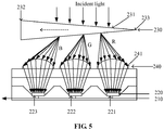
microlens layer 240. Themicrolens layer 240 is located between thepixel array layer 220 and themicroprism layer 230. Themicroprisms 231 are configured to decompose the incident light into the m color lights for emission, andmicrolenses 241 in themicrolens layer 240 are configured to independently converge each type of color light of the n color lights in the m color lights emitted by themicroprisms 231 for respective emission into the subpixels in the corresponding colors of the pixels corresponding to themicroprisms 231.
In an implementation mode shown inFig. 5 , eachmicrolens 241 corresponds to a subpixel. Descriptions will be made still with the condition that a pixel includes three subpixels as an example. Then, the red light emitted by themicroprism 231 is converged by themicrolens 241 for emission into thered subpixel 221 of the pixel corresponding to themicroprism 231, the emitted green light is converged by themicrolens 241 for emission into thegreen subpixel 222 of the pixel, and the emitted blue light is converged by themicrolens 241 for emission into theblue subpixel 223 of the pixel.
Themicrolens layer 240 is located between thepixel array layer 220 and themicroprism layer 230, then themicrolens layer 240 may independently converge each type of color light in the n color lights emitted by themicroprism layer 230 for respective emission into the subpixels in the corresponding colors of the pixels corresponding to themicroprisms 231, and complete emission of each color light into the subpixels in the corresponding colors may be ensured, so that the light transmittance of the subpixels is improved, and the exposure time required by imaging is reduced. - 2) In a second position relationship, the camera photosensitive component further includes the
microlens layer 240, themicrolens layer 240 is opposite and parallel to themicroprism layer 230, and themicrolens layer 240 is nonadjacent to thepixel array layer 220. Themicrolenses 241 in themicrolens layer 240 are configured to converge the incident light for emission; and themicroprisms 231 are configured to decompose the converged light emitted by themicrolenses 241 into the m color lights for emission, and the n color lights in the emitted m color lights are emitted into the subpixels in the corresponding colors of the pixels corresponding to themicroprisms 241. - In an implementation mode, each
microlens 241 corresponds to a subpixel, referring toFig. 6 . Descriptions will be made still with the condition that a pixel includes three subpixels as an example. Then, themicroprism 231 decomposes the incident light converged by themicrolens 241 into seven color lights for emission, the emitted red light is emitted into thered subpixel 221 of the pixel corresponding to themicroprism 231, the emitted green light is emitted into thegreen subpixel 222 of the pixel, and the emitted blue light is emitted into theblue subpixel 223 of the pixel. - There are multiple manners for manufacturing the
microprism layer 230. Descriptions will be made in the aspect with two of them as examples. - 1) In a first manufacturing manner, the
microprism layer 230 is formed by arranging eachmicroprism 231. For example, the microprisms may be arranged in a grid corresponding to pixels the pixel array layer. In this case,microprisms 231 with same or approximately same sizes of the pixels may be manufactured and arranged according to the position relationship between eachmicroprism 231 and the pixel, to form themicroprism layer 230. - 2) In a second manufacturing manner, it is relatively difficult to manufacture
microprisms 231 with same or approximately same sizes of the pixels and arrange themicroprisms 231, so that themicrorprism layer 230 is formed by etching a substrate made from a preset material. In this case, etching may be performed according to the position relationships between themicroprisms 231 and the pixels, to form themicroprism layer 230. The preset material may be optical glass, quartz glass, an alkali halide crystal, plastics and the like, which will not be limited in the aspect. - From the above, according to the camera photosensitive component provided by the present disclosure, the microprisms decompose the incident light into the m color lights for emission, and the n color lights in the emitted m color lights are emitted into the subpixels in the corresponding colors of the pixels corresponding to the microprisms respectively. In such a manner, the n color lights may be formed by decomposition with the microprisms, not obtained after part of color light is absorbed by an RGB filter, and the transmittance of the color light emitted into the pixels may be improved, so that the exposure time required by imaging is reduced, the camera shooting effect under the low-lighting condition may further be improved, and the camera shooting effect on the moving object may also be improved.
- In one example, the first pixels and the second pixels share the nth subpixels. Accordingly, the shared subpixels have relatively large areas, and the photosensitive areas of the subpixels may be enlarged. Therefore, the light transmittance of the subpixels is improved, and the exposure time required by imaging is reduced.
- The microlens layer is located between the pixel array layer and the microprism layer, then the microlens layer may independently converge each type of color light of the n color lights emitted by the microprism layer for respective emission into the subpixels in the corresponding colors of the pixels corresponding to the microprisms, and complete emission of each color light into the subpixels in the corresponding colors may be ensured, so that the light transmittance of the subpixels is improved, and the exposure time required by imaging is reduced.
- The microprism layer is formed by etching the substrate made from the preset material, so that it is unnecessary to manufacture and arrange microprisms with same or approximately same sizes of the pixels, and difficulties in implementation of the microprism layer may be reduced.
-
Fig. 7 is a block diagram of adevice 700 carrying a camera photosensitive component, according to an exemplary aspect. For example, thedevice 700 may be a mobile phone, a computer, a digital broadcast terminal, a messaging device, a gaming console, a tablet, a medical device, exercise equipment, a personal digital assistant, and the like. - Referring to
Fig. 7 , thedevice 700 may include one or more of the following components: aprocessing component 702, amemory 704, apower component 706, amultimedia component 708, anaudio component 710, an Input/Output (I/O)interface 712, asensor component 714, and acommunication component 716. - The
processing component 702 typically controls overall operations of thedevice 700, such as the operations associated with display, telephone calls, data communications, camera operations, and recording operations. Theprocessing component 702 may include one ormore processors 718 to execute instructions to perform all or part of the steps in the abovementioned method. Moreover, theprocessing component 702 may include one or more modules which facilitate interaction between theprocessing component 702 and the other components. For instance, theprocessing component 702 may include a multimedia module to facilitate interaction between themultimedia component 708 and theprocessing component 702. - The
memory 704 is configured to store various types of data to support the operation of thedevice 700. Examples of such data include instructions for any application programs or methods operated on thedevice 700, contact data, phonebook data, messages, pictures, video, etc. Thememory 704 may be implemented by any type of volatile or non-volatile memory devices, or a combination thereof, such as a Static Random Access Memory (SRAM), an Electrically Erasable Programmable Read-Only Memory (EEPROM), an Erasable Programmable Read-Only Memory (EPROM), a Programmable Read-Only Memory (PROM), a Read-Only Memory (ROM), a magnetic memory, a flash memory, and a magnetic or optical disk. - The
power component 706 provides power for various components of thedevice 700. Thepower component 706 may include a power management system, one or more power supplies, and other components associated with the generation, management and distribution of power for thedevice 700. - The
multimedia component 708 includes a screen providing an output interface between thedevice 700 and a user. In some aspects, the screen may include a Liquid Crystal Display (LCD) and a Touch Panel (TP). If the screen includes the TP, the screen may be implemented as a touch screen to receive an input signal from the user. The TP includes one or more touch sensors to sense touches, swipes and gestures on the TP. The touch sensors may not only sense a boundary of a touch or swipe action, but also detect a duration and pressure associated with the touch or swipe action. In some aspects, themultimedia component 708 includes a front camera and/or a rear camera. The front camera and/or the rear camera may receive external multimedia data when thedevice 700 is in an operation mode, such as a photographing mode or a video mode. Each of the front camera and the rear camera may be a fixed optical lens system or have focusing and optical zooming capabilities. - The
audio component 710 is configured to output and/or input an audio signal. For example, theaudio component 710 includes a Microphone (MIC), and the MIC is configured to receive an external audio signal when thedevice 700 is in the operation mode, such as a call mode, a recording mode and a voice recognition mode. The received audio signal may be further stored in thememory 704 or sent through thecommunication component 716. In some aspects, theaudio component 710 further includes a speaker configured to output the audio signal. - The I/
O interface 712 provides an interface between theprocessing component 702 and a peripheral interface module, and the peripheral interface module may be a keyboard, a click wheel, a button and the like. The button may include, but not limited to: a home button, a volume button, a starting button and a locking button. - The
sensor component 714 includes one or more sensors configured to provide status assessment in various aspects for thedevice 700. For instance, thesensor component 714 may detect an on/off status of thedevice 700 and relative positioning of components, such as a display and small keyboard of thedevice 700, and thesensor component 714 may further detect a change in a position of thedevice 700 or a component of thedevice 700, presence or absence of contact between the user and thedevice 700, orientation or acceleration/deceleration of thedevice 700 and a change in temperature of thedevice 700. Thesensor component 714 may include a proximity sensor configured to detect presence of an object nearby without any physical contact. Thesensor component 714 may also include a light sensor, such as a Complementary Metal Oxide Semiconductor (CMOS) or Charge Coupled Device (CCD) image sensor, configured for use in an imaging application. Thesensor component 714 may include camera photosensitive component disclosed above. In some aspects, thesensor component 714 may also include an acceleration sensor, a gyroscope sensor, a magnetic sensor, a pressure sensor or a temperature sensor. - The
communication component 716 is configured to facilitate wired or wireless communication between thedevice 700 and other equpment. Thedevice 700 may access a communication-standard-based wireless network, such as a Wireless Fidelity (WiFi) network, a 2nd-Generation (2G) or 3rd-Generation (3G) network or a combination thereof. In an exemplary aspect, thecommunication component 716 receives a broadcast signal or broadcast associated information from an external broadcast management system through a broadcast channel. In an exemplary aspect, thecommunication component 716 further includes a Near Field Communication (NFC) module to facilitate short-range communication. For example, the NFC module may be implemented on the basis of a Radio Frequency Identification (RFID) technology, an Infrared Data Association (IrDA) technology, an Ultra-WideBand (UWB) technology, a Bluetooth (BT) technology and another technology. - In an exemplary aspect, the
device 700 may be implemented by one or more Application Specific Integrated Circuits (ASICs), Digital Signal Processors (DSPs), Digital Signal Processing Devices (DSPDs), Programmable Logic Devices (PLDs), Field Programmable Gate Arrays (FPGAs), controllers, micro-controllers, microprocessors or other electronic components, and is configured to execute the abovementioned method. - In an exemplary aspect, there is also provided a non-transitory computer-readable storage medium including an instruction, such as the
memory 704 including an instruction, and the instruction may be executed by theprocessor 718 of thedevice 700 to implement the abovementioned method. For example, the non-transitory computer-readable storage medium may be a ROM, a Random Access Memory (RAM), a Compact Disc Read-Only Memory (CD-ROM), a magnetic tape, a floppy disc, optical data storage equipment and the like. - The technical solutions provided by the aspects of the present disclosure may achieve the following beneficial effects.
- The microprisms decompose the incident light into the m color lights for emission, and the n color lights in the emitted m color lights are respectively emitted into the subpixels in the corresponding colors of the pixels corresponding to the microprisms. In such a manner, the n color lights may be formed by decomposition with the microprisms, not obtained after part of color light is absorbed by an RGB filter, and transmittance of the color light emitted into the pixels may be improved, so that an exposure time required for imaging is reduced, a camera shooting effect under a low-lighting condition may further be improved, and the camera shooting effect on a moving object may also be improved.
- The first pixels and the second pixels share the nth subpixels. Accordingly, the shared subpixels have relatively large areas, and photosensitive areas of the subpixels may be enlarged. Therefore, light transmittance of the subpixels is improved, and the exposure time required for imaging is reduced.
- The microlens layer is located between the pixel array layer and the microprism layer, then the microlens layer may independently converge each type of color light of the n color lights emitted by the microprism layer for respective emission into the subpixels in the corresponding colors of the pixels corresponding to the microprisms, and complete emission of each type of color light into the subpixels in the corresponding colors may be ensured, so that the light transmittance of the subpixels is improved, and the exposure time required for imaging is reduced.
- The microprism layer is formed by etching the substrate made from the preset material, so that it is unnecessary to manufacture and arrange microprisms with same or approximately same sizes of the pixels, and difficulties in implementation of the microprism layer may be reduced.
- Other aspects of the present disclosure will be apparent to those skilled in the art from consideration of the specification and practice of the present disclosure. This application is intended to cover any variations, uses, or adaptations of the present disclosure following the general principles thereof and including such departures from the present disclosure as come within known or customary practice in the art. It is intended that the specification and examples be considered as exemplary only, with a true scope and spirit of the present disclosure being indicated by the following claims.
- It will be appreciated that the present disclosure is not limited to the exact construction that has been described above and illustrated in the accompanying drawings, and that various modifications and changes may be made without departing from the scope thereof. It is intended that the scope of the present invention only be limited by the appended claims.
Claims (13)
- A camera photosensitive component, characterized in that the camera photosensitive component comprises:a silicon substrate layer (210);a pixel array layer (220) attached to one surface of the silicon substrate layer (210); anda microprism layer (230) arranged in parallel with the pixel array layer (220), the microprism layer (230) comprising microprisms,wherein the microprisms in the microprism layer (230) are configured to decompose incident light into m color lights for emission, and n color lights in the emitted m color lights are respectively emitted into subpixels in corresponding colors of pixels corresponding to the microprisms, and n is not greater than m.
- The camera photosensitive component of claim 1, wherein each microprism corresponds to a pixel in the pixel array layer (220), and the pixel comprises n subpixels; and
the microprism is configured to decompose the incident light into the m color lights for emission, and the n color lights in the emitted m color lights are emitted into the subpixels in the corresponding colors of the pixel. - The camera photosensitive component of claim 2, wherein a bottom surface of the microprism is perpendicular to a plane where the pixel array layer (220) is located, and the n subpixels arranged in ascending order of refractive indexes of the corresponding colors are sequentially arranged in the pixel along a direction from a vertex of the microprism towards the bottom surface.
- The camera photosensitive component of claim 1, wherein every two adjacent microprisms correspond to two adjacent pixels: a first pixel and a second pixel; wherein each of the first pixel and the second pixel comprises n subpixels, and the nth subpixels in the first pixel and the second pixel are adjacent; and
whererin the first microprism is configured to decompose the incident light into the m color lights for emission, the n color lights in the emitted m color lights are respectively emitted into the subpixels in the corresponding colors of the first pixel, the second microprism is configured to decompose the incident light into the m color lights for emission, and the n color lights in the emitted m color lights are respectively emitted into the subpixels in the corresponding colors of the second pixel. - The camera photosensitive component of claim 4, wherein a bottom surface of the first microprism is opposite and parallel to a bottom surface of the second microprism, the bottom surface of the first microprism is perpendicular to the plane where the pixel array layer (220) is located, and the bottom surface of the second microprism is perpendicular to the plane where the pixel array layer (220) is located; and
wherein the n subpixels arranged in ascending order of refractive indexes of the corresponding colors are sequentially arranged in the first pixel along a direction from a vertex of the first microprism towards the bottom surface of the first microprism, and the n subpixels arranged in ascending order of refractive indexes of the corresponding colors are sequentially arranged in the second pixel along a direction from a vertex of the second microprism points towards the bottom surface of the second microprism. - The camera photosensitive component of claim 1, wherein every two adjacent microprisms correspond to two adjacent pixels: a first pixel and a second pixel; wherein the first pixel and the second pixel comprises totally 2n-1 subpixels, and the first pixel and the second pixel share the nth subpixel; and
wherein the first microprism is configured to decompose the incident light into the m color lights for emission, the n color lights in the emitted m color lights are respectively emitted into n-1 subpixels in the corresponding colors of the first pixel and the shared nth subpixel, the second microprism is configured to decompose the incident light into the m color lights for emission, and the n color lights in the emitted m color lights are respectively emitted into n-1 subpixels in the corresponding colors of the second pixel and the shared nth subpixel. - The camera photosensitive component of claim 6, wherein a bottom surface of the first microprism is opposite and parallel to a bottom surface of the second microprism, the bottom surface of the first microprism is perpendicular to the plane where the pixel array layer (220) is located, and the bottom surface of the second microprism is perpendicular to the plane where the pixel array layer (220) is located; and
the n-1 subpixels arranged in ascending order of refractive indexes of the corresponding colors and the shared nth subpixel are sequentially arranged in the first pixel along a direction from a vertex of the first microprism to the bottom surface of the first microprism, and the n-1 subpixels arranged in ascending order of refractive indexes of the corresponding colors and the shared nth subpixel are sequentially arranged in the second pixel along a direction from a vertex of the second microprism to the bottom surface of the second microprism. - The camera photosensitive component of claim 1, further comprising a microlens layer (240) located between the pixel array layer (220) and the microprism layer (230);
wherein the microprisms are configured to decompose the incident light into the m color lights for emission; and
wherein microlenses in the microlens layer (240) are configured to independently converge each type of color light of the n color lights in the m color lights emitted by the microprisms for respective emission into the subpixels in the corresponding colors of the pixels corresponding to the microprisms. - The camera photosensitive component of claim 1, further comprising a microlens layer (240), wherein the microlens layer (240) is parallel to the microprism layer (230), and the microlens layer is nonadjacent to the pixel array layer (220);
wherein microlenses in the microlens layer (240) are configured to converge the incident light for emission; and
wherein the microprisms are configured to decompose the converged light emitted by the microlenses into the m color lights for emission, and the n color lights in the emitted m color lights are emitted into the subpixels in the corresponding colors of the pixels corresponding to the microprisms. - The camera photosensitive component of any one of claims 1-9, wherein the microprism layer (230) comprises an array of microprisms arranged in a grid corresponding to the pixel array layer (220).
- The camera photosensitive component of any one of claims 1-9, wherein the microprism layer (230) is formed by etching a substrate made from a preset material according to preset position relationships between the microprisms and the pixels in the pixel array layer (220).
- A camera, comprising the camera photosensitive component of any one of claims 1-11.
- A camera shooting terminal, comprising the camera of claim 12.
Applications Claiming Priority (1)
| Application Number | Priority Date | Filing Date | Title |
|---|---|---|---|
| CN201711025227.1A CN107613182A (en) | 2017-10-27 | 2017-10-27 | Camera photosensitive components, cameras and camera terminals |
Publications (2)
| Publication Number | Publication Date |
|---|---|
| EP3477704A1 true EP3477704A1 (en) | 2019-05-01 |
| EP3477704B1 EP3477704B1 (en) | 2021-12-01 |
Family
ID=61080183
Family Applications (1)
| Application Number | Title | Priority Date | Filing Date |
|---|---|---|---|
| EP18201616.2A Active EP3477704B1 (en) | 2017-10-27 | 2018-10-19 | Camera photosensitive component, camera, and camera shooting terminal |
Country Status (7)
| Country | Link |
|---|---|
| US (1) | US10727263B2 (en) |
| EP (1) | EP3477704B1 (en) |
| JP (1) | JP6738904B2 (en) |
| KR (1) | KR102172944B1 (en) |
| CN (1) | CN107613182A (en) |
| RU (1) | RU2686578C1 (en) |
| WO (1) | WO2019080397A1 (en) |
Cited By (1)
| Publication number | Priority date | Publication date | Assignee | Title |
|---|---|---|---|---|
| EP3990877A4 (en) * | 2019-06-28 | 2023-08-02 | Mantis Photonics AB | OPTICAL SPECTROMETER AND METHOD FOR SPECTRALLY RESOLVED TWO-DIMENSIONAL IMAGING OF AN OBJECT |
Families Citing this family (4)
| Publication number | Priority date | Publication date | Assignee | Title |
|---|---|---|---|---|
| CN107613182A (en) * | 2017-10-27 | 2018-01-19 | 北京小米移动软件有限公司 | Camera photosensitive components, cameras and camera terminals |
| CN109034039B (en) * | 2018-07-19 | 2021-04-23 | 维沃移动通信有限公司 | A display module and terminal equipment |
| CN111614878B (en) * | 2020-05-26 | 2022-04-22 | 维沃移动通信(杭州)有限公司 | Pixel unit, photoelectric sensor, camera module and electronic equipment |
| CN114422730B (en) * | 2022-01-17 | 2024-03-19 | 惠州Tcl移动通信有限公司 | Image sensor and electronic device |
Citations (3)
| Publication number | Priority date | Publication date | Assignee | Title |
|---|---|---|---|---|
| US5210400A (en) * | 1990-07-17 | 1993-05-11 | Kabushiki Kaisha Toshiba | Solid-state imaging device applicable to high sensitivity color camera and using diffraction gratings |
| CN105304668A (en) * | 2015-11-11 | 2016-02-03 | 武汉新芯集成电路制造有限公司 | CMOS image sensor |
| CN106908993A (en) * | 2017-03-06 | 2017-06-30 | 合肥鑫晟光电科技有限公司 | A kind of backlight module and liquid crystal display |
Family Cites Families (19)
| Publication number | Priority date | Publication date | Assignee | Title |
|---|---|---|---|---|
| US6104446A (en) * | 1996-12-18 | 2000-08-15 | Blankenbecler; Richard | Color separation optical plate for use with LCD panels |
| JPH11313334A (en) * | 1998-04-27 | 1999-11-09 | Nippon Hoso Kyokai <Nhk> | Solid-state imaging device |
| US7176446B1 (en) * | 1999-09-15 | 2007-02-13 | Zoran Corporation | Method and apparatus for distributing light onto electronic image sensors |
| JP2001309395A (en) * | 2000-04-21 | 2001-11-02 | Sony Corp | Solid-state imaging device and method of manufacturing the same |
| JP2004172335A (en) * | 2002-11-20 | 2004-06-17 | Sony Corp | Solid-state imaging device |
| CN100496095C (en) * | 2006-04-26 | 2009-06-03 | 中国科学院自动化研究所 | High Speed Camera System Based on Distributed Data Transmission |
| US7813045B2 (en) * | 2006-06-02 | 2010-10-12 | Sabic Innovative Plastics Ip B.V. | Prism pitch optimization |
| CN101101432B (en) * | 2006-07-06 | 2011-06-08 | 曹嘉灿 | Optical module |
| CN100544008C (en) * | 2006-09-27 | 2009-09-23 | 采钰科技股份有限公司 | image module, image sensing device and manufacturing method thereof |
| JP2008153518A (en) * | 2006-12-19 | 2008-07-03 | Hitachi Kokusai Electric Inc | Solid-state imaging device and camera device using the same |
| US8384818B2 (en) * | 2008-06-18 | 2013-02-26 | Panasonic Corporation | Solid-state imaging device including arrays of optical elements and photosensitive cells |
| US8581174B2 (en) * | 2008-08-26 | 2013-11-12 | Omnivision Technologies, Inc. | Image sensor with prismatic de-multiplexing |
| CN102033330B (en) * | 2009-09-25 | 2016-01-20 | 三星电子株式会社 | High speed optical shutter and method of operating thereof and optical devices |
| CN101986432B (en) * | 2010-10-25 | 2015-04-01 | 上海华虹宏力半导体制造有限公司 | Cmos image sensor |
| CN102510447B (en) * | 2011-09-28 | 2016-08-10 | 上海华虹宏力半导体制造有限公司 | Imageing sensor |
| CN104641626B (en) * | 2012-09-19 | 2018-02-27 | 富士胶片株式会社 | Camera device and focus confirmation display method |
| GB2516967A (en) * | 2013-08-09 | 2015-02-11 | Iq Structures Sro | Autostereoscopic prismatic printing rasters |
| US9632572B2 (en) * | 2013-10-03 | 2017-04-25 | Leap Motion, Inc. | Enhanced field of view to augment three-dimensional (3D) sensory space for free-space gesture interpretation |
| CN107613182A (en) * | 2017-10-27 | 2018-01-19 | 北京小米移动软件有限公司 | Camera photosensitive components, cameras and camera terminals |
-
2017
- 2017-10-27 CN CN201711025227.1A patent/CN107613182A/en active Pending
-
2018
- 2018-01-30 WO PCT/CN2018/074525 patent/WO2019080397A1/en not_active Ceased
- 2018-01-30 JP JP2018544922A patent/JP6738904B2/en active Active
- 2018-01-30 RU RU2018127558A patent/RU2686578C1/en active
- 2018-01-30 KR KR1020187037980A patent/KR102172944B1/en active Active
- 2018-05-21 US US15/984,818 patent/US10727263B2/en active Active
- 2018-10-19 EP EP18201616.2A patent/EP3477704B1/en active Active
Patent Citations (4)
| Publication number | Priority date | Publication date | Assignee | Title |
|---|---|---|---|---|
| US5210400A (en) * | 1990-07-17 | 1993-05-11 | Kabushiki Kaisha Toshiba | Solid-state imaging device applicable to high sensitivity color camera and using diffraction gratings |
| CN105304668A (en) * | 2015-11-11 | 2016-02-03 | 武汉新芯集成电路制造有限公司 | CMOS image sensor |
| CN106908993A (en) * | 2017-03-06 | 2017-06-30 | 合肥鑫晟光电科技有限公司 | A kind of backlight module and liquid crystal display |
| WO2018161669A1 (en) * | 2017-03-06 | 2018-09-13 | 京东方科技集团股份有限公司 | Backlight module and liquid crystal display device |
Cited By (1)
| Publication number | Priority date | Publication date | Assignee | Title |
|---|---|---|---|---|
| EP3990877A4 (en) * | 2019-06-28 | 2023-08-02 | Mantis Photonics AB | OPTICAL SPECTROMETER AND METHOD FOR SPECTRALLY RESOLVED TWO-DIMENSIONAL IMAGING OF AN OBJECT |
Also Published As
| Publication number | Publication date |
|---|---|
| KR102172944B1 (en) | 2020-11-03 |
| US10727263B2 (en) | 2020-07-28 |
| WO2019080397A1 (en) | 2019-05-02 |
| US20190131335A1 (en) | 2019-05-02 |
| EP3477704B1 (en) | 2021-12-01 |
| JP2020500431A (en) | 2020-01-09 |
| RU2686578C1 (en) | 2019-04-29 |
| JP6738904B2 (en) | 2020-08-12 |
| KR20190085850A (en) | 2019-07-19 |
| CN107613182A (en) | 2018-01-19 |
Similar Documents
| Publication | Publication Date | Title |
|---|---|---|
| EP3477704B1 (en) | Camera photosensitive component, camera, and camera shooting terminal | |
| US10672851B2 (en) | Display panel and photoelectric detection method | |
| EP3627484A1 (en) | Organic light-emitting diode display, display control method and electronic device | |
| US10818736B2 (en) | Display substrate of electronic device and method for manufacturing same | |
| RU2736269C1 (en) | Terminal screen, terminal screen control method and terminal | |
| CN110392146A (en) | terminal screen and terminal | |
| US11514710B2 (en) | Display panel and terminal device | |
| US20210405384A1 (en) | Optical processing apparatus, camera module, electronic device and capturing method | |
| CN209787228U (en) | Terminal screen and terminal | |
| US11029910B2 (en) | Terminal screen and terminal | |
| US11425299B2 (en) | Camera module, processing method and apparatus, electronic device, and storage medium | |
| CN209859047U (en) | Terminal screen and terminal | |
| US10935850B1 (en) | Display panel, manufacturing method, and electronic device | |
| US9753319B2 (en) | Liquid crystal display including display panel that includes wires and protruding spacers | |
| CN112684644B (en) | Display panels and electronic devices | |
| CN108510924A (en) | Display panel, photoelectric detecting method, device and computer readable storage medium | |
| CN112213898A (en) | Color image acquisition equipment and electronic equipment | |
| CN215771150U (en) | Display module and terminal equipment | |
| CN112684639A (en) | Display panel, manufacturing method thereof and electronic equipment | |
| CN111381705B (en) | A terminal | |
| CN114095672A (en) | Imaging system, method and electronic device |
Legal Events
| Date | Code | Title | Description |
|---|---|---|---|
| PUAI | Public reference made under article 153(3) epc to a published international application that has entered the european phase |
Free format text: ORIGINAL CODE: 0009012 |
|
| STAA | Information on the status of an ep patent application or granted ep patent |
Free format text: STATUS: THE APPLICATION HAS BEEN PUBLISHED |
|
| AK | Designated contracting states |
Kind code of ref document: A1 Designated state(s): AL AT BE BG CH CY CZ DE DK EE ES FI FR GB GR HR HU IE IS IT LI LT LU LV MC MK MT NL NO PL PT RO RS SE SI SK SM TR |
|
| AX | Request for extension of the european patent |
Extension state: BA ME |
|
| STAA | Information on the status of an ep patent application or granted ep patent |
Free format text: STATUS: REQUEST FOR EXAMINATION WAS MADE |
|
| 17P | Request for examination filed |
Effective date: 20191029 |
|
| RBV | Designated contracting states (corrected) |
Designated state(s): AL AT BE BG CH CY CZ DE DK EE ES FI FR GB GR HR HU IE IS IT LI LT LU LV MC MK MT NL NO PL PT RO RS SE SI SK SM TR |
|
| STAA | Information on the status of an ep patent application or granted ep patent |
Free format text: STATUS: EXAMINATION IS IN PROGRESS |
|
| 17Q | First examination report despatched |
Effective date: 20210319 |
|
| GRAP | Despatch of communication of intention to grant a patent |
Free format text: ORIGINAL CODE: EPIDOSNIGR1 |
|
| STAA | Information on the status of an ep patent application or granted ep patent |
Free format text: STATUS: GRANT OF PATENT IS INTENDED |
|
| GRAJ | Information related to disapproval of communication of intention to grant by the applicant or resumption of examination proceedings by the epo deleted |
Free format text: ORIGINAL CODE: EPIDOSDIGR1 |
|
| GRAP | Despatch of communication of intention to grant a patent |
Free format text: ORIGINAL CODE: EPIDOSNIGR1 |
|
| INTG | Intention to grant announced |
Effective date: 20210611 |
|
| INTG | Intention to grant announced |
Effective date: 20210701 |
|
| GRAS | Grant fee paid |
Free format text: ORIGINAL CODE: EPIDOSNIGR3 |
|
| GRAA | (expected) grant |
Free format text: ORIGINAL CODE: 0009210 |
|
| STAA | Information on the status of an ep patent application or granted ep patent |
Free format text: STATUS: THE PATENT HAS BEEN GRANTED |
|
| AK | Designated contracting states |
Kind code of ref document: B1 Designated state(s): AL AT BE BG CH CY CZ DE DK EE ES FI FR GB GR HR HU IE IS IT LI LT LU LV MC MK MT NL NO PL PT RO RS SE SI SK SM TR |
|
| REG | Reference to a national code |
Ref country code: GB Ref legal event code: FG4D |
|
| REG | Reference to a national code |
Ref country code: AT Ref legal event code: REF Ref document number: 1452623 Country of ref document: AT Kind code of ref document: T Effective date: 20211215 Ref country code: CH Ref legal event code: EP |
|
| REG | Reference to a national code |
Ref country code: IE Ref legal event code: FG4D |
|
| REG | Reference to a national code |
Ref country code: DE Ref legal event code: R096 Ref document number: 602018027418 Country of ref document: DE |
|
| REG | Reference to a national code |
Ref country code: LT Ref legal event code: MG9D |
|
| REG | Reference to a national code |
Ref country code: NL Ref legal event code: MP Effective date: 20211201 |
|
| REG | Reference to a national code |
Ref country code: AT Ref legal event code: MK05 Ref document number: 1452623 Country of ref document: AT Kind code of ref document: T Effective date: 20211201 |
|
| PG25 | Lapsed in a contracting state [announced via postgrant information from national office to epo] |
Ref country code: RS Free format text: LAPSE BECAUSE OF FAILURE TO SUBMIT A TRANSLATION OF THE DESCRIPTION OR TO PAY THE FEE WITHIN THE PRESCRIBED TIME-LIMIT Effective date: 20211201 Ref country code: LT Free format text: LAPSE BECAUSE OF FAILURE TO SUBMIT A TRANSLATION OF THE DESCRIPTION OR TO PAY THE FEE WITHIN THE PRESCRIBED TIME-LIMIT Effective date: 20211201 Ref country code: FI Free format text: LAPSE BECAUSE OF FAILURE TO SUBMIT A TRANSLATION OF THE DESCRIPTION OR TO PAY THE FEE WITHIN THE PRESCRIBED TIME-LIMIT Effective date: 20211201 Ref country code: BG Free format text: LAPSE BECAUSE OF FAILURE TO SUBMIT A TRANSLATION OF THE DESCRIPTION OR TO PAY THE FEE WITHIN THE PRESCRIBED TIME-LIMIT Effective date: 20220301 Ref country code: AT Free format text: LAPSE BECAUSE OF FAILURE TO SUBMIT A TRANSLATION OF THE DESCRIPTION OR TO PAY THE FEE WITHIN THE PRESCRIBED TIME-LIMIT Effective date: 20211201 |
|
| PG25 | Lapsed in a contracting state [announced via postgrant information from national office to epo] |
Ref country code: SE Free format text: LAPSE BECAUSE OF FAILURE TO SUBMIT A TRANSLATION OF THE DESCRIPTION OR TO PAY THE FEE WITHIN THE PRESCRIBED TIME-LIMIT Effective date: 20211201 Ref country code: PL Free format text: LAPSE BECAUSE OF FAILURE TO SUBMIT A TRANSLATION OF THE DESCRIPTION OR TO PAY THE FEE WITHIN THE PRESCRIBED TIME-LIMIT Effective date: 20211201 Ref country code: NO Free format text: LAPSE BECAUSE OF FAILURE TO SUBMIT A TRANSLATION OF THE DESCRIPTION OR TO PAY THE FEE WITHIN THE PRESCRIBED TIME-LIMIT Effective date: 20220301 Ref country code: LV Free format text: LAPSE BECAUSE OF FAILURE TO SUBMIT A TRANSLATION OF THE DESCRIPTION OR TO PAY THE FEE WITHIN THE PRESCRIBED TIME-LIMIT Effective date: 20211201 Ref country code: HR Free format text: LAPSE BECAUSE OF FAILURE TO SUBMIT A TRANSLATION OF THE DESCRIPTION OR TO PAY THE FEE WITHIN THE PRESCRIBED TIME-LIMIT Effective date: 20211201 Ref country code: GR Free format text: LAPSE BECAUSE OF FAILURE TO SUBMIT A TRANSLATION OF THE DESCRIPTION OR TO PAY THE FEE WITHIN THE PRESCRIBED TIME-LIMIT Effective date: 20220302 Ref country code: ES Free format text: LAPSE BECAUSE OF FAILURE TO SUBMIT A TRANSLATION OF THE DESCRIPTION OR TO PAY THE FEE WITHIN THE PRESCRIBED TIME-LIMIT Effective date: 20211201 |
|
| PG25 | Lapsed in a contracting state [announced via postgrant information from national office to epo] |
Ref country code: NL Free format text: LAPSE BECAUSE OF FAILURE TO SUBMIT A TRANSLATION OF THE DESCRIPTION OR TO PAY THE FEE WITHIN THE PRESCRIBED TIME-LIMIT Effective date: 20211201 |
|
| PG25 | Lapsed in a contracting state [announced via postgrant information from national office to epo] |
Ref country code: SM Free format text: LAPSE BECAUSE OF FAILURE TO SUBMIT A TRANSLATION OF THE DESCRIPTION OR TO PAY THE FEE WITHIN THE PRESCRIBED TIME-LIMIT Effective date: 20211201 Ref country code: SK Free format text: LAPSE BECAUSE OF FAILURE TO SUBMIT A TRANSLATION OF THE DESCRIPTION OR TO PAY THE FEE WITHIN THE PRESCRIBED TIME-LIMIT Effective date: 20211201 Ref country code: RO Free format text: LAPSE BECAUSE OF FAILURE TO SUBMIT A TRANSLATION OF THE DESCRIPTION OR TO PAY THE FEE WITHIN THE PRESCRIBED TIME-LIMIT Effective date: 20211201 Ref country code: PT Free format text: LAPSE BECAUSE OF FAILURE TO SUBMIT A TRANSLATION OF THE DESCRIPTION OR TO PAY THE FEE WITHIN THE PRESCRIBED TIME-LIMIT Effective date: 20220401 Ref country code: EE Free format text: LAPSE BECAUSE OF FAILURE TO SUBMIT A TRANSLATION OF THE DESCRIPTION OR TO PAY THE FEE WITHIN THE PRESCRIBED TIME-LIMIT Effective date: 20211201 Ref country code: CZ Free format text: LAPSE BECAUSE OF FAILURE TO SUBMIT A TRANSLATION OF THE DESCRIPTION OR TO PAY THE FEE WITHIN THE PRESCRIBED TIME-LIMIT Effective date: 20211201 |
|
| REG | Reference to a national code |
Ref country code: DE Ref legal event code: R097 Ref document number: 602018027418 Country of ref document: DE |
|
| PG25 | Lapsed in a contracting state [announced via postgrant information from national office to epo] |
Ref country code: IS Free format text: LAPSE BECAUSE OF FAILURE TO SUBMIT A TRANSLATION OF THE DESCRIPTION OR TO PAY THE FEE WITHIN THE PRESCRIBED TIME-LIMIT Effective date: 20220401 |
|
| PLBE | No opposition filed within time limit |
Free format text: ORIGINAL CODE: 0009261 |
|
| STAA | Information on the status of an ep patent application or granted ep patent |
Free format text: STATUS: NO OPPOSITION FILED WITHIN TIME LIMIT |
|
| PG25 | Lapsed in a contracting state [announced via postgrant information from national office to epo] |
Ref country code: DK Free format text: LAPSE BECAUSE OF FAILURE TO SUBMIT A TRANSLATION OF THE DESCRIPTION OR TO PAY THE FEE WITHIN THE PRESCRIBED TIME-LIMIT Effective date: 20211201 Ref country code: AL Free format text: LAPSE BECAUSE OF FAILURE TO SUBMIT A TRANSLATION OF THE DESCRIPTION OR TO PAY THE FEE WITHIN THE PRESCRIBED TIME-LIMIT Effective date: 20211201 |
|
| 26N | No opposition filed |
Effective date: 20220902 |
|
| PG25 | Lapsed in a contracting state [announced via postgrant information from national office to epo] |
Ref country code: SI Free format text: LAPSE BECAUSE OF FAILURE TO SUBMIT A TRANSLATION OF THE DESCRIPTION OR TO PAY THE FEE WITHIN THE PRESCRIBED TIME-LIMIT Effective date: 20211201 |
|
| PG25 | Lapsed in a contracting state [announced via postgrant information from national office to epo] |
Ref country code: MC Free format text: LAPSE BECAUSE OF FAILURE TO SUBMIT A TRANSLATION OF THE DESCRIPTION OR TO PAY THE FEE WITHIN THE PRESCRIBED TIME-LIMIT Effective date: 20211201 Ref country code: IT Free format text: LAPSE BECAUSE OF FAILURE TO SUBMIT A TRANSLATION OF THE DESCRIPTION OR TO PAY THE FEE WITHIN THE PRESCRIBED TIME-LIMIT Effective date: 20211201 |
|
| REG | Reference to a national code |
Ref country code: CH Ref legal event code: PL |
|
| REG | Reference to a national code |
Ref country code: BE Ref legal event code: MM Effective date: 20221031 |
|
| P01 | Opt-out of the competence of the unified patent court (upc) registered |
Effective date: 20230523 |
|
| PG25 | Lapsed in a contracting state [announced via postgrant information from national office to epo] |
Ref country code: LU Free format text: LAPSE BECAUSE OF NON-PAYMENT OF DUE FEES Effective date: 20221019 |
|
| PG25 | Lapsed in a contracting state [announced via postgrant information from national office to epo] |
Ref country code: LI Free format text: LAPSE BECAUSE OF NON-PAYMENT OF DUE FEES Effective date: 20221031 Ref country code: CH Free format text: LAPSE BECAUSE OF NON-PAYMENT OF DUE FEES Effective date: 20221031 |
|
| PG25 | Lapsed in a contracting state [announced via postgrant information from national office to epo] |
Ref country code: BE Free format text: LAPSE BECAUSE OF NON-PAYMENT OF DUE FEES Effective date: 20221031 |
|
| PG25 | Lapsed in a contracting state [announced via postgrant information from national office to epo] |
Ref country code: IE Free format text: LAPSE BECAUSE OF NON-PAYMENT OF DUE FEES Effective date: 20221019 |
|
| PG25 | Lapsed in a contracting state [announced via postgrant information from national office to epo] |
Ref country code: HU Free format text: LAPSE BECAUSE OF FAILURE TO SUBMIT A TRANSLATION OF THE DESCRIPTION OR TO PAY THE FEE WITHIN THE PRESCRIBED TIME-LIMIT; INVALID AB INITIO Effective date: 20181019 |
|
| PG25 | Lapsed in a contracting state [announced via postgrant information from national office to epo] |
Ref country code: CY Free format text: LAPSE BECAUSE OF FAILURE TO SUBMIT A TRANSLATION OF THE DESCRIPTION OR TO PAY THE FEE WITHIN THE PRESCRIBED TIME-LIMIT Effective date: 20211201 |
|
| PG25 | Lapsed in a contracting state [announced via postgrant information from national office to epo] |
Ref country code: MK Free format text: LAPSE BECAUSE OF FAILURE TO SUBMIT A TRANSLATION OF THE DESCRIPTION OR TO PAY THE FEE WITHIN THE PRESCRIBED TIME-LIMIT Effective date: 20211201 |
|
| PG25 | Lapsed in a contracting state [announced via postgrant information from national office to epo] |
Ref country code: TR Free format text: LAPSE BECAUSE OF FAILURE TO SUBMIT A TRANSLATION OF THE DESCRIPTION OR TO PAY THE FEE WITHIN THE PRESCRIBED TIME-LIMIT Effective date: 20211201 |
|
| PG25 | Lapsed in a contracting state [announced via postgrant information from national office to epo] |
Ref country code: MT Free format text: LAPSE BECAUSE OF FAILURE TO SUBMIT A TRANSLATION OF THE DESCRIPTION OR TO PAY THE FEE WITHIN THE PRESCRIBED TIME-LIMIT Effective date: 20211201 |
|
| REG | Reference to a national code |
Ref country code: DE Ref legal event code: R079 Ref document number: 602018027418 Country of ref document: DE Free format text: PREVIOUS MAIN CLASS: H01L0027146000 Ipc: H10F0039180000 |
|
| PGFP | Annual fee paid to national office [announced via postgrant information from national office to epo] |
Ref country code: DE Payment date: 20251021 Year of fee payment: 8 |
|
| PGFP | Annual fee paid to national office [announced via postgrant information from national office to epo] |
Ref country code: GB Payment date: 20251022 Year of fee payment: 8 |
|
| PGFP | Annual fee paid to national office [announced via postgrant information from national office to epo] |
Ref country code: FR Payment date: 20251030 Year of fee payment: 8 |