EP3474295A1 - Electrode structure, electronic device comprising same and method for manufacturing same - Google Patents
Electrode structure, electronic device comprising same and method for manufacturing same Download PDFInfo
- Publication number
- EP3474295A1 EP3474295A1 EP17813464.9A EP17813464A EP3474295A1 EP 3474295 A1 EP3474295 A1 EP 3474295A1 EP 17813464 A EP17813464 A EP 17813464A EP 3474295 A1 EP3474295 A1 EP 3474295A1
- Authority
- EP
- European Patent Office
- Prior art keywords
- pattern
- light blocking
- auxiliary electrode
- organic insulating
- layer
- Prior art date
- Legal status (The legal status is an assumption and is not a legal conclusion. Google has not performed a legal analysis and makes no representation as to the accuracy of the status listed.)
- Granted
Links
Images



Classifications
-
- H—ELECTRICITY
- H05—ELECTRIC TECHNIQUES NOT OTHERWISE PROVIDED FOR
- H05B—ELECTRIC HEATING; ELECTRIC LIGHT SOURCES NOT OTHERWISE PROVIDED FOR; CIRCUIT ARRANGEMENTS FOR ELECTRIC LIGHT SOURCES, IN GENERAL
- H05B33/00—Electroluminescent light sources
- H05B33/12—Light sources with substantially two-dimensional [2D] radiating surfaces
- H05B33/26—Light sources with substantially two-dimensional [2D] radiating surfaces characterised by the composition or arrangement of the conductive material used as an electrode
- H05B33/28—Light sources with substantially two-dimensional [2D] radiating surfaces characterised by the composition or arrangement of the conductive material used as an electrode of translucent electrodes
-
- H—ELECTRICITY
- H01—ELECTRIC ELEMENTS
- H01B—CABLES; CONDUCTORS; INSULATORS; SELECTION OF MATERIALS FOR THEIR CONDUCTIVE, INSULATING OR DIELECTRIC PROPERTIES
- H01B1/00—Conductors or conductive bodies characterised by the conductive materials; Selection of materials as conductors
- H01B1/02—Conductors or conductive bodies characterised by the conductive materials; Selection of materials as conductors mainly consisting of metals or alloys
-
- H—ELECTRICITY
- H01—ELECTRIC ELEMENTS
- H01B—CABLES; CONDUCTORS; INSULATORS; SELECTION OF MATERIALS FOR THEIR CONDUCTIVE, INSULATING OR DIELECTRIC PROPERTIES
- H01B13/00—Apparatus or processes specially adapted for manufacturing conductors or cables
-
- H—ELECTRICITY
- H01—ELECTRIC ELEMENTS
- H01B—CABLES; CONDUCTORS; INSULATORS; SELECTION OF MATERIALS FOR THEIR CONDUCTIVE, INSULATING OR DIELECTRIC PROPERTIES
- H01B13/00—Apparatus or processes specially adapted for manufacturing conductors or cables
- H01B13/0026—Apparatus for manufacturing conducting or semi-conducting layers, e.g. deposition of metal
-
- H—ELECTRICITY
- H01—ELECTRIC ELEMENTS
- H01B—CABLES; CONDUCTORS; INSULATORS; SELECTION OF MATERIALS FOR THEIR CONDUCTIVE, INSULATING OR DIELECTRIC PROPERTIES
- H01B13/00—Apparatus or processes specially adapted for manufacturing conductors or cables
- H01B13/0036—Details
-
- H—ELECTRICITY
- H01—ELECTRIC ELEMENTS
- H01B—CABLES; CONDUCTORS; INSULATORS; SELECTION OF MATERIALS FOR THEIR CONDUCTIVE, INSULATING OR DIELECTRIC PROPERTIES
- H01B7/00—Insulated conductors or cables characterised by their form
-
- H—ELECTRICITY
- H01—ELECTRIC ELEMENTS
- H01B—CABLES; CONDUCTORS; INSULATORS; SELECTION OF MATERIALS FOR THEIR CONDUCTIVE, INSULATING OR DIELECTRIC PROPERTIES
- H01B7/00—Insulated conductors or cables characterised by their form
- H01B7/0009—Details relating to the conductive cores
-
- H—ELECTRICITY
- H10—SEMICONDUCTOR DEVICES; ELECTRIC SOLID-STATE DEVICES NOT OTHERWISE PROVIDED FOR
- H10K—ORGANIC ELECTRIC SOLID-STATE DEVICES
- H10K50/00—Organic light-emitting devices
- H10K50/10—OLEDs or polymer light-emitting diodes [PLED]
- H10K50/18—Carrier blocking layers
-
- H—ELECTRICITY
- H10—SEMICONDUCTOR DEVICES; ELECTRIC SOLID-STATE DEVICES NOT OTHERWISE PROVIDED FOR
- H10K—ORGANIC ELECTRIC SOLID-STATE DEVICES
- H10K50/00—Organic light-emitting devices
- H10K50/80—Constructional details
- H10K50/805—Electrodes
- H10K50/81—Anodes
- H10K50/814—Anodes combined with auxiliary electrodes, e.g. ITO layer combined with metal lines
-
- H—ELECTRICITY
- H10—SEMICONDUCTOR DEVICES; ELECTRIC SOLID-STATE DEVICES NOT OTHERWISE PROVIDED FOR
- H10K—ORGANIC ELECTRIC SOLID-STATE DEVICES
- H10K50/00—Organic light-emitting devices
- H10K50/80—Constructional details
- H10K50/805—Electrodes
- H10K50/82—Cathodes
- H10K50/824—Cathodes combined with auxiliary electrodes
-
- H—ELECTRICITY
- H10—SEMICONDUCTOR DEVICES; ELECTRIC SOLID-STATE DEVICES NOT OTHERWISE PROVIDED FOR
- H10K—ORGANIC ELECTRIC SOLID-STATE DEVICES
- H10K50/00—Organic light-emitting devices
- H10K50/80—Constructional details
- H10K50/805—Electrodes
- H10K50/82—Cathodes
- H10K50/828—Transparent cathodes, e.g. comprising thin metal layers
-
- H—ELECTRICITY
- H10—SEMICONDUCTOR DEVICES; ELECTRIC SOLID-STATE DEVICES NOT OTHERWISE PROVIDED FOR
- H10K—ORGANIC ELECTRIC SOLID-STATE DEVICES
- H10K71/00—Manufacture or treatment specially adapted for the organic devices covered by this subclass
- H10K71/621—Providing a shape to conductive layers, e.g. patterning or selective deposition
Definitions
- the present specification relates to an electrode structure, an electronic device including the electrode structure, and a method of manufacturing the electrode structure.
- a transparent electrode is applied to a region of an effective screen part, in an electronic device, such as a display or a touch panel, is increased, and to this end, a a metal oxide-series transparent conductive layer, such as an ITO, an IZO, and a ZnO, is used, but the transparent conductive layer based on the metal oxide has low endogenetic conductivity of the material itself and thus has a fetal problem in making the electronic device be large.
- auxiliary electrode pattern that is a metal electrode having low resistance together with a transparent electrode based on an oxide is developed.
- the present specification provides an electrode structure, an electronic device including the electrode structure, and a method of manufacturing the electrode structure.
- the present specification provides an electrode structure including: a transparent electrode; a light blocking pattern provided on the transparent electrode; an auxiliary electrode pattern provided on the light blocking pattern; and an organic insulating pattern covering the light blocking pattern and the auxiliary electrode pattern, in which a line width of the light blocking pattern is larger than a line width of the auxiliary electrode pattern.
- the present specification provides an electronic device including the electrode structure.
- the present specification provides a method of manufacturing the electrode structure, the method including forming an electrode structure, in which the light blocking pattern, the auxiliary electrode pattern, and the organic insulating pattern are sequentially provided on the transparent electrode.
- the present specification provides an electrode structure including: a transparent electrode; a light blocking pattern provided on the transparent electrode; an auxiliary electrode pattern provided on the light blocking pattern; and an organic insulating pattern covering the light blocking pattern and the auxiliary electrode pattern.
- the transparent electrode is not particularly limited as long as the transparent electrode has transparency in which the predetermined quantity or more of light may permeate, and for example, the transparent electrode may be an oxide-based transparent electrode layer, a thin metal layer, a metal oxide pattern, or a metal pattern. Particularly, the transparent electrode may be an oxide-based transparent electrode layer.
- the oxide-based transparent electrode layer may include a transparent metal oxide, and for example, the oxide-based transparent electrode layer may include at least one of a zinc oxide, an indium oxide, a tin oxide, an indium-tin oxide (ITO), and an indium zinc oxide (IZO).
- a transparent metal oxide for example, the oxide-based transparent electrode layer may include at least one of a zinc oxide, an indium oxide, a tin oxide, an indium-tin oxide (ITO), and an indium zinc oxide (IZO).
- a thickness of the transparent electrode is not particularly limited as long as the transparent electrode has transparency in which the predetermined quantity or more of light may permeate, and particularly, a thickness of the transparent electrode may be 10 nm or more and 500 nm or less.
- the light blocking pattern is formed of a material which is capable of blocking light, and as long as the material is capable of blocking light and is an easy material for forming a pattern, the material is not particularly limited, and the light blocking pattern may be formed of a material generally used in the art.
- the light blocking pattern may be a metal pattern or a conductive polymer pattern, and preferably, may be a metal pattern.
- the metal pattern means a pattern including a metal, and may include a metal oxide, a metal nitride, and the like as well as pure metal.
- a line width W2 of the light blocking pattern may be larger than a line width W1 of the auxiliary electrode pattern.
- a line width of the light blocking pattern may be larger than a line width of the auxiliary electrode pattern by 0.5 ⁇ m or more, and more particularly, a line width of the light blocking pattern may be larger than a line width of the auxiliary electrode pattern by 0.5 ⁇ m or more and 10 ⁇ m or less.
- the line width of the light blocking pattern is not particularly limited, but particularly, the line width of the light blocking pattern may be 2.0 ⁇ m or more and 1.0 mm or less.
- the light blocking pattern may have a minimum thickness in which light may be blocked during exposure, and particularly, a thickness of the light blocking pattern may be 100 nm or less, and more particularly, a thickness of the light blocking pattern may be 20 nm or more and 100 nm or less.
- the light blocking pattern provided between the transparent electrode and the auxiliary electrode may have electric conductivity.
- the light blocking pattern and the auxiliary electrode pattern may include different metals.
- the light blocking pattern and the auxiliary electrode pattern may include metals of which etching speeds for an etchant are different from each other.
- the light blocking pattern and the auxiliary electrode pattern may be different from each other, and may independently include chrome (Cr), molybdenum (Mo), aluminum (Al), copper (Cu), silver (Ag), and an alloy thereof.
- the light blocking pattern may include aluminum and the auxiliary electrode pattern may include copper, and more particularly, the light blocking pattern may be formed of aluminum and the auxiliary electrode pattern may be formed of copper.
- a thickness of the auxiliary electrode pattern is not particularly limited, but when a thickness of the auxiliary electrode pattern is increased, resistance is further decreased. In the present specification, there is an advantage in that even though a thickness of the auxiliary electrode pattern is increased, the auxiliary electrode pattern is easily insulated.
- a thickness of the auxiliary electrode pattern may be 100 nm or more and 2 ⁇ m or less, and particularly, 300 nm or more and 500 nm or less.
- the line width of the auxiliary electrode pattern is not particularly limited, but particularly, the line width of the auxiliary electrode pattern may be 1.5 ⁇ m or more and 1 mm or less.
- a form of the auxiliary electrode pattern is not particularly limited, and a form, which is not viewed by the eyes of a user or does not distort light by the auxiliary electrode pattern, is preferable.
- an irregular pattern is advantageous, but the irregular pattern may be viewed by the eyes of the user as if being biased to one side, so that the auxiliary electrode pattern may be a homogeneous pattern in which regularity and irregularity are appropriately harmonized.
- a predetermined size of area is designated as a basic unit in an area, in which the pattern is to be put, the points are irregularly disposed while the number of points within the basic unit is uniformly adjusted, and the points are connected to form a homogeneous pattern in which regularity and irregularity are appropriately harmonized.
- the method of forming the pattern by connecting the homogeneously disposed points is not particularly limited, but for example, the points for forming the auxiliary electrode pattern may be connected by using a Voronoi diagram generator or a Delaunay pattern generator to form the pattern.
- the light blocking pattern and the organic insulating pattern are provided in response to the auxiliary electrode pattern.
- the light blocking pattern and the organic insulating pattern have the same form as that of the auxiliary electrode pattern, but are provided in a state where only the line widths of the light blocking pattern and the organic insulating pattern are larger than that of the auxiliary electrode pattern.
- a line width W3 of the organic insulating pattern may be larger than the line width W2 of the light blocking pattern.
- a line width of the organic insulating pattern may be larger than a line width of the light blocking pattern by 0.5 ⁇ m or more, and more particularly, a line width of the organic insulating pattern may be larger than a line width of the light blocking pattern by 0.5 ⁇ m or more and 2 ⁇ m or less.
- a length of the shortest line connected from one point among the corners of the light blocking pattern to an opposite surface of a surface that is in contact with the light blocking pattern of the organic insulating pattern may be 0.5 ⁇ m or more.
- the light blocking pattern may secure insulation stability by the organic insulating pattern.
- a length of the shortest line connected from one point among the corners of the auxiliary electrode pattern to an opposite surface of a surface that is in contact with the auxiliary electrode pattern of the organic insulating pattern may be 0.5 ⁇ m or more.
- the auxiliary electrode pattern may secure insulation stability by the organic insulating pattern.
- the opposite surface of the surface of the organic insulating pattern that is in contact with the light blocking pattern and the auxiliary electrode pattern may be a curved surface.
- the curved surface means a streamline shape surface having no angular part.
- the organic insulating pattern may include at least one of a novolac-based polymer, a poly hydroxyl styrene-based polymer, a polyimide-based polymer, an acryl-based polymer, and a poly siloxane-based polymer, and particularly, the organic insulating pattern may include a polyimide-based polymer.
- the insulating pattern cannot completely cover the auxiliary electrode pattern or the auxiliary electrode pattern is not formed with the thickness in which insulation stability is secured.
- the insulating pattern may not cover the auxiliary electrode pattern with a sufficient thickness, in which insulation stability is secured, due to a step of the auxiliary electrode pattern.
- the auxiliary electrode pattern is not covered by the insulation pattern, so that an exposed surface of the auxiliary electrode pattern may be generated as illustrated in the image of the SEM of FIG. 6 .
- the insulation pattern of the present specification has an advantage in stably insulating the auxiliary electrode pattern regardless of a thickness of the auxiliary electrode pattern.
- the light blocking pattern may have a thickness of 100 nm or less and electric conductivity, and the light blocking pattern and the auxiliary electrode pattern may be different from each other and independently include chrome (Cr), molybdenum (Mo), aluminum (Al), copper (Cu), silver (Ag), and an alloy thereof, and the organic insulating pattern may include a polyimide-based polymer and has a larger line width than that of the light blocking pattern, and the opposite surface of the surface that is in contact with the light blocking pattern and the auxiliary electrode pattern of the organic insulating pattern may be a curved surface. In this case, even though a thickness of the auxiliary electrode pattern is increased, the organic insulating pattern may stably insulate the auxiliary electrode pattern.
- the present specification provides an electronic device including the electrode structure.
- the electronic device includes the electrode structure
- the electronic device is not particularly limited, but the electronic device may be any one of a plasma display panel (PDP), a light emitting diode (LED), an organic light emitting diode (OLED), a liquid crystal display (LCD), a color filter on thin film transistor-liquid crystal display (COT-LCD), a thin film transistor-liquid crystal display (LCD-TFT), and a cathode ray tube (CRT).
- PDP plasma display panel
- LED light emitting diode
- OLED organic light emitting diode
- LCD liquid crystal display
- COT-LCD color filter on thin film transistor-liquid crystal display
- LCD-TFT thin film transistor-liquid crystal display
- CRT cathode ray tube
- the present specification provides a display device including the electrode structure.
- the present specification provides a lighting device including the electrode structure.
- the lighting device may be a white lighting device or a color lighting device.
- the present specification provides a method of manufacturing the electrode structure, the method including forming the electrode structure, in which the light blocking pattern, the auxiliary electrode pattern, and the organic insulating pattern are sequentially provided on the transparent electrode.
- the method of manufacturing the electrode structure may quote the description of the electrode structure.
- the forming of the electrode structure may include: S1) forming the light blocking pattern and the auxiliary electrode pattern on the transparent electrode; and S2) forming the organic insulating pattern covering the light blocking pattern and the auxiliary electrode pattern.
- the method of forming each of the light blocking pattern and the auxiliary electrode pattern on the transparent electrode is not particularly limited as long as the method may form the light blocking pattern and the auxiliary electrode pattern on the transparent electrode, and for example, the method may be a roll-printing method, an inkjet printing method, a screen printing method, a deposition method, a photolithography method, and an etching method, and the like, and an etching method is preferable.
- Operation S1) may include: S1-1) forming a light blocking layer on the transparent electrode; S1-2) forming an auxiliary electrode layer on the light blocking layer; S1-3) forming an etching protecting pattern on the auxiliary electrode layer; and S1-4) forming the light blocking pattern and the auxiliary electrode pattern by removing portions of the light blocking layer and the auxiliary electrode layer, in which the etching protecting pattern is not formed, through one or more times of an etching process.
- the method of forming the light blocking layer is not particularly limited, and the light blocking layer may be formed by a method generally used in the art.
- the method of forming the light blocking layer may be any one of a plating deposition method, a sputter deposition method, and an evaporator deposition method.
- a composition for the light blocking layer may include at least one of chrome (Cr), molybdenum (Mo), aluminum (Al), copper (Cu), silver (Ag), and an alloy thereof, and particularly, may include at least one of aluminum (Al), molybdenum (Mo), chrome (Cr), and an alloy thereof.
- the method of forming the auxiliary electrode layer is not particularly limited, and the auxiliary electrode layer may be formed by a method generally used in the art.
- the method of forming the auxiliary electrode layer may be any one of a plating deposition method, a sputter deposition method, and an evaporator deposition method.
- a composition for the auxiliary electrode layer may include at least one of chrome (Cr), molybdenum (Mo), aluminum (Al), copper (Cu), silver (Ag), and an alloy thereof, and particularly, may include at least one of copper (Cu), aluminum (Al), silver (Ag), and an alloy thereof.
- the method of forming the etching protecting pattern is not particularly limited, and the etching protecting pattern may be formed by a method generally used in the art. Particularly, the method of forming the etching protecting pattern may be any one of a roll printing method, an inkjet printing method, a screen printing method, and a photolithography method.
- the method of forming the etching protecting pattern may include a method of directly forming the etching protecting pattern on the auxiliary electrode layer by using a composition for the etching protecting pattern, or a method of forming an etching protecting layer on the auxiliary electrode layer by using a composition for the etching protecting pattern and developing the etching protecting layer to form the pattern.
- the composition for the etching protecting pattern may include an etching resistant polymer and a solvent.
- the etching resistant polymer may include at least one of a novolac-based polymer and a poly hydroxyl styrene-based polymer.
- the composition for the etching protecting pattern may further include at least one of a cross linking agent, a diazonaphtho quinone-series photoactive material, and an initiator.
- the composition for the etching protecting pattern may be a positive photosensitive material composition or a negative photosensitive material composition, and is not specially limited.
- the solvent, the cross linking agent, and the initiator are not specially limited, and may adopt a solvent, a cross linking agent, and an initiator generally used in the art.
- the patterns may be formed by a one-time etching process with a collective etchant, or the patterns may be formed by two or more times of etching process with two or more kinds of etchant.
- operation S1-4) may be an operation of forming the light blocking pattern and the auxiliary electrode pattern by removing the portions of the light blocking layer and the auxiliary electrode layer, in which the etching protecting pattern is not formed, by a one-time etching process with collective etchant.
- a line width of the light blocking pattern may be larger than a line width of the auxiliary electrode pattern by a difference in an etching speed of the light blocking layer and the auxiliary electrode layer with respect to the collective etchant.
- the etchant may etch each of the light blocking layer and the auxiliary electrode layer
- the etchant is not particularly limited, but an etchant generally used in the art may be selected according to the materials of the light blocking layer and the auxiliary electrode layer.
- the collective etchant may etch both the light blocking layer and the auxiliary electrode layer
- the collective etchant is not particularly limited, but a use of an etchant generally used in the art may be selected according to the materials of the light blocking layer and the auxiliary electrode layer.
- the collective etchant may include at least one of a mixed acid etchant, in which phosphoric acid, nitric acid, and acetic acid are mixed; an iron chloride-series etchant; a copper chloride-series etchant; a sulfuric acid hydrogen peroxide mixture-based etchant; a hydrochloric acid-based etchant; and an organic acid-series etchant.
- the collective etchant which is capable of etching both aluminum and copper may be any one of a mixture acid-based etchant, in which phosphoric acid, nitric acid, and acetic acid are mixed, and an iron chloride-series etchant.
- Operation S2) may include: S2-1) forming a photosensitive organic insulating layer on a surface provided with the light blocking pattern and the auxiliary electrode pattern of the transparent electrode; S2-2) performing an exposure by irradiating light from an opposite surface of the surface provided with the photosensitive organic insulating layer of the transparent electrode; S2-3) forming a precursor of the organic insulating pattern on the surface provided with the light blocking pattern and the auxiliary electrode pattern of the transparent electrode, by developing the exposed photosensitive organic insulating layer; and S2-4) performing a reflow for forming the organic insulating pattern covering the light blocking pattern and the auxiliary electrode pattern by heating the precursor of the organic insulating pattern.
- Operation S2-1) is an operation of forming a photosensitive organic insulating layer by using a composition for a photosensitive organic insulating layer on a surface provided with the light blocking pattern and the auxiliary electrode pattern of the transparent electrode.
- the method of forming the photosensitive organic insulating layer is not particularly limited, and the photosensitive organic insulating layer may be formed by a method generally used in the art. Particularly, the method of forming the photosensitive organic insulating layer may be any one of a dip coating method, a spray coating method, a spin coating method, and a slit coating method.
- the composition for the photosensitive organic insulating layer may include an insulating polymer, a diazonaphtho quinone-series photoactive material, and a solvent, and the composition for the photosensitive organic insulating layer may be a positive photosensitive material composition.
- the insulating polymer is not particularly limited, but for example, the insulating polymer may include at least one of a novolac-based polymer, a poly hydroxyl styrene-based polymer, a polyimide-based polymer, an acryl-based polymer, and a poly siloxane-based polymer.
- the exposure is performed by irradiating light to the transparent electrode, and particularly, light is radiated to the opposite surface of the surface provided with the photosensitive organic insulating layer of the transparent electrode so that light may be selectively exposed to the photosensitive organic insulating layer by the light blocking pattern on the substrate.
- light is radiated to the opposite surface of the surface provided with the light blocking pattern and the photosensitive organic insulating layer of the transparent electrode, so that light permeates only a region, in which the light blocking pattern is not formed, and thus a part of the photosensitive organic insulating layer formed in the region, in which the light blocking pattern is not formed, may be exposed by the permeating light.
- the part of the photosensitive organic insulating layer exposed by the light in the performing of the exposure may be changed to have a property developed by a developer.
- the exposure condition may be adjusted according to a property of the composition for the applied photosensitive organic insulating layer, and is not particularly limited.
- Operation S2-3) is an operation, in which a part of the exposed photosensitive organic insulating layer exposed to light by the developer is removed to form a precursor of the organic insulating pattern on the light blocking pattern.
- the developer is not particularly limited, and a developer generally used in the art may be adopted.
- the temperature is not particularly limited, but particularly, the temperature may be 130°C or more and 250°C or less.
- Operation S2 may further include S2-5) curing the organic insulating pattern.
- a temperature of curing the organic insulating pattern is not particularly limited, but particularly, the temperature may be 130°C or more and 250°C or less.
- the method of manufacturing the electrode structure may further include forming the transparent electrode on the substrate before operation S1-1).
- the method of forming the transparent electrode is not particularly limited, but may be any one of a sputter deposition method and a chemical vapor deposition method.
- the forming of the electrode structure may include: S1-1) forming a light blocking layer on the transparent electrode; S1-2) forming an auxiliary electrode layer on the light blocking layer; S1-3) forming an etching protecting pattern on the auxiliary electrode layer; S1-4) forming the light blocking pattern and the auxiliary electrode pattern by removing portions of the light blocking layer and the auxiliary electrode layer, in which the etching protecting pattern is not formed, through a one-time etching process by using collective etchant; S2-1) forming a photosensitive organic insulating layer on a surface provided with the light blocking pattern and the auxiliary electrode pattern of the transparent electrode; S2-2) performing exposure of irradiating light from an opposite surface of the surface provided with the photosensitive organic insulating layer of the transparent electrode; S2-3) forming a precursor of an organic insulating pattern on the surface provided with the light blocking pattern and the auxiliary electrode pattern of the transparent electrode, by developing the exposed photosensitive organic insulating layer; S2-4) performing a reflow of forming the organic insulating
- An aluminum layer (light blocking layer) having a thickness of 100 nm was formed on an ITO film having a thickness of 23 nm by a sputter deposition method, and a copper layer (auxiliary electrode layer) having a thickness of 500 nm was formed on the aluminum layer by an evaporation deposition method.
- An etching protecting pattern was formed on the copper layer by a reverse offset printing process by using a composition for the etching protecting pattern based on a novolac resin.
- An aluminum pattern and a copper pattern was formed by removing portions of the aluminum layer and the copper layer, in which the etching protecting pattern is not formed, by using a mixed acid etchant, in which phosphoric acid, nitric acid, and acetic acid are mixed, and the copper pattern was additionally etched by using a sulfuric acid hydrogen peroxide mixture-based copper etchant.
- a mixed acid etchant in which phosphoric acid, nitric acid, and acetic acid are mixed
- the copper pattern was additionally etched by using a sulfuric acid hydrogen peroxide mixture-based copper etchant.
- a line width of the aluminum pattern is larger than that of the copper pattern through FIG. 3 .
- a photosensitive polyimide layer was formed by using a photosensitive polyimide composition on the aluminum pattern and the copper pattern, and then light was radiated from an opposite surface of a surface provided with the aluminum pattern and the copper pattern of the ITO film.
- the photosensitive polyimide layer was developed with a developer of 2.38 wt% of tetramethylammonium hydroxide(TMAH) to form an organic insulating pattern precursor.
- TMAH tetramethylammonium hydroxide
- an organic insulating pattern precursor was identically manufactured to Example 1. It can be seen that the organic insulating pattern precursor formed on a copper pattern by using a copper pattern (auxiliary electrode pattern) as a light blocking pattern has a smaller line width than that of the copper pattern.
- Example 1 it can be seen that the aluminum pattern and the copper pattern are covered in five minutes and the organic insulating pattern precursor flows down after 20 minutes to be formed with a curved surface, but in Comparative Example 1, it can be seen that the copper pattern is not completely covered even after 20 minutes, so that a non-insulating region is generated.
Landscapes
- Physics & Mathematics (AREA)
- Optics & Photonics (AREA)
- Engineering & Computer Science (AREA)
- Manufacturing & Machinery (AREA)
- Electroluminescent Light Sources (AREA)
- Internal Circuitry In Semiconductor Integrated Circuit Devices (AREA)
- Manufacturing Of Electric Cables (AREA)
Abstract
Description
- This application claims priority to and the benefit of Korean Patent Application No.
10-2016-0075924 - The present specification relates to an electrode structure, an electronic device including the electrode structure, and a method of manufacturing the electrode structure.
- Recently, demands for a product, in which a transparent electrode is applied to a region of an effective screen part, in an electronic device, such as a display or a touch panel, are increased, and to this end, a a metal oxide-series transparent conductive layer, such as an ITO, an IZO, and a ZnO, is used, but the transparent conductive layer based on the metal oxide has low endogenetic conductivity of the material itself and thus has a fetal problem in making the electronic device be large. Particularly, in developing an OLED lighting device which is recently getting the spotlight, due to a high resistance characteristic of a transparent electrode based on an oxide, there is a problem in that when a size of the device is increased, non-uniformity of the quantity of current is caused by a carrier crowding phenomenon. The problem causes a sharp decrease in brightness uniformity and induces the local generation of high heat during an operation of the device to decrease a life of the device due to thermal degradation of an organic material.
- In order to solve the problem, a technology for an auxiliary electrode pattern that is a metal electrode having low resistance together with a transparent electrode based on an oxide is developed.
- The present specification provides an electrode structure, an electronic device including the electrode structure, and a method of manufacturing the electrode structure.
- The present specification provides an electrode structure including: a transparent electrode; a light blocking pattern provided on the transparent electrode; an auxiliary electrode pattern provided on the light blocking pattern; and an organic insulating pattern covering the light blocking pattern and the auxiliary electrode pattern, in which a line width of the light blocking pattern is larger than a line width of the auxiliary electrode pattern.
- Further, the present specification provides an electronic device including the electrode structure.
- Further, the present specification provides a method of manufacturing the electrode structure, the method including forming an electrode structure, in which the light blocking pattern, the auxiliary electrode pattern, and the organic insulating pattern are sequentially provided on the transparent electrode.
- According to the present invention, it is possible to easily implement an organic insulating pattern having a form surrounding a metal auxiliary electrode pattern.
-
-
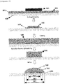
FIG. 1 is a flowchart illustrating a process of forming an auxiliary electrode pattern and an insulating pattern in the related art. -
FIG. 2 is a flowchart illustrating a process of forming a light blocking pattern, an auxiliary electrode pattern, and an insulating pattern according to an exemplary embodiment of the present specification. -
FIG. 3 is an image of a scanning electron microscope (SEM) of a light blocking pattern and an auxiliary electrode pattern formed in Example 1. -
FIG. 4 is an image of an SEM of an organic insulating pattern precursor formed on an auxiliary electrode pattern in Comparative Example 1. -
FIG. 5 is an image of an SEM of an organic insulating pattern precursor formed on a light blocking pattern and an auxiliary electrode pattern in Example 1. -
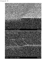
FIG. 6 is an image of an SEM of the organic insulating pattern precursor reflowing for five minutes or 20 minutes in Comparative Example 1. -
FIG. 7 is an image of an SEM of the organic insulating pattern precursor reflowing for five minutes or 20 minutes in Example 1. -
- 1: Transparent electrode
- 2: Auxiliary electrode layer
- 3: Etching protecting pattern
- 4: Auxiliary electrode pattern
- 5: Organic insulating precursor layer
- 6: Precursor of organic insulating pattern
- 7: Organic insulating pattern
- 100: Transparent electrode
- 200: Light blocking layer
- 210: Light blocking pattern
- 300: Auxiliary electrode layer
- 310: Auxiliary electrode pattern
- 400: Etching protecting pattern
- 500: Organic insulating precursor layer
- 510: Precursor of organic insulating pattern
- 520: Organic insulating pattern
- W1: Line width of auxiliary electrode pattern
- W2: Line width of light blocking pattern
- W3: Line width of organic insulating pattern
- Hereinafter, the present specification will be described in detail.
- The present specification provides an electrode structure including: a transparent electrode; a light blocking pattern provided on the transparent electrode; an auxiliary electrode pattern provided on the light blocking pattern; and an organic insulating pattern covering the light blocking pattern and the auxiliary electrode pattern.
- The transparent electrode is not particularly limited as long as the transparent electrode has transparency in which the predetermined quantity or more of light may permeate, and for example, the transparent electrode may be an oxide-based transparent electrode layer, a thin metal layer, a metal oxide pattern, or a metal pattern. Particularly, the transparent electrode may be an oxide-based transparent electrode layer.
- The oxide-based transparent electrode layer may include a transparent metal oxide, and for example, the oxide-based transparent electrode layer may include at least one of a zinc oxide, an indium oxide, a tin oxide, an indium-tin oxide (ITO), and an indium zinc oxide (IZO).
- A thickness of the transparent electrode is not particularly limited as long as the transparent electrode has transparency in which the predetermined quantity or more of light may permeate, and particularly, a thickness of the transparent electrode may be 10 nm or more and 500 nm or less.
- The light blocking pattern is formed of a material which is capable of blocking light, and as long as the material is capable of blocking light and is an easy material for forming a pattern, the material is not particularly limited, and the light blocking pattern may be formed of a material generally used in the art. For example, the light blocking pattern may be a metal pattern or a conductive polymer pattern, and preferably, may be a metal pattern. In this case, the metal pattern means a pattern including a metal, and may include a metal oxide, a metal nitride, and the like as well as pure metal.
- A line width W2 of the light blocking pattern may be larger than a line width W1 of the auxiliary electrode pattern. Particularly, a line width of the light blocking pattern may be larger than a line width of the auxiliary electrode pattern by 0.5 µm or more, and more particularly, a line width of the light blocking pattern may be larger than a line width of the auxiliary electrode pattern by 0.5 µm or more and 10 µm or less.
- When a line width of the light blocking pattern is larger than a line width of the auxiliary electrode pattern, the line width of the light blocking pattern is not particularly limited, but particularly, the line width of the light blocking pattern may be 2.0 µm or more and 1.0 mm or less.
- The light blocking pattern may have a minimum thickness in which light may be blocked during exposure, and particularly, a thickness of the light blocking pattern may be 100 nm or less, and more particularly, a thickness of the light blocking pattern may be 20 nm or more and 100 nm or less.
- In order for the auxiliary electrode to be electrically connected with the transparent electrode to serve to decrease resistance, the light blocking pattern provided between the transparent electrode and the auxiliary electrode may have electric conductivity.
- The light blocking pattern and the auxiliary electrode pattern may include different metals. Particularly, the light blocking pattern and the auxiliary electrode pattern may include metals of which etching speeds for an etchant are different from each other.
- The light blocking pattern and the auxiliary electrode pattern may be different from each other, and may independently include chrome (Cr), molybdenum (Mo), aluminum (Al), copper (Cu), silver (Ag), and an alloy thereof. Particularly, the light blocking pattern may include aluminum and the auxiliary electrode pattern may include copper, and more particularly, the light blocking pattern may be formed of aluminum and the auxiliary electrode pattern may be formed of copper.
- A thickness of the auxiliary electrode pattern is not particularly limited, but when a thickness of the auxiliary electrode pattern is increased, resistance is further decreased. In the present specification, there is an advantage in that even though a thickness of the auxiliary electrode pattern is increased, the auxiliary electrode pattern is easily insulated. A thickness of the auxiliary electrode pattern may be 100 nm or more and 2 µm or less, and particularly, 300 nm or more and 500 nm or less.
- When a line width of the auxiliary electrode pattern is smaller than a line width of the light blocking pattern, the line width of the auxiliary electrode pattern is not particularly limited, but particularly, the line width of the auxiliary electrode pattern may be 1.5 µm or more and 1 mm or less.
- A form of the auxiliary electrode pattern is not particularly limited, and a form, which is not viewed by the eyes of a user or does not distort light by the auxiliary electrode pattern, is preferable. In order to minimize diffraction/interference, an irregular pattern is advantageous, but the irregular pattern may be viewed by the eyes of the user as if being biased to one side, so that the auxiliary electrode pattern may be a homogeneous pattern in which regularity and irregularity are appropriately harmonized.
- When points for forming the auxiliary electrode pattern are disposed, a predetermined size of area is designated as a basic unit in an area, in which the pattern is to be put, the points are irregularly disposed while the number of points within the basic unit is uniformly adjusted, and the points are connected to form a homogeneous pattern in which regularity and irregularity are appropriately harmonized. The method of forming the pattern by connecting the homogeneously disposed points is not particularly limited, but for example, the points for forming the auxiliary electrode pattern may be connected by using a Voronoi diagram generator or a Delaunay pattern generator to form the pattern.
- The light blocking pattern and the organic insulating pattern are provided in response to the auxiliary electrode pattern. Particularly, the light blocking pattern and the organic insulating pattern have the same form as that of the auxiliary electrode pattern, but are provided in a state where only the line widths of the light blocking pattern and the organic insulating pattern are larger than that of the auxiliary electrode pattern.
- A line width W3 of the organic insulating pattern may be larger than the line width W2 of the light blocking pattern. Particularly, a line width of the organic insulating pattern may be larger than a line width of the light blocking pattern by 0.5 µm or more, and more particularly, a line width of the organic insulating pattern may be larger than a line width of the light blocking pattern by 0.5 µm or more and 2 µm or less.
- A length of the shortest line connected from one point among the corners of the light blocking pattern to an opposite surface of a surface that is in contact with the light blocking pattern of the organic insulating pattern may be 0.5 µm or more. In this case, the light blocking pattern may secure insulation stability by the organic insulating pattern.
- A length of the shortest line connected from one point among the corners of the auxiliary electrode pattern to an opposite surface of a surface that is in contact with the auxiliary electrode pattern of the organic insulating pattern may be 0.5 µm or more. In this case, the auxiliary electrode pattern may secure insulation stability by the organic insulating pattern.
- The opposite surface of the surface of the organic insulating pattern that is in contact with the light blocking pattern and the auxiliary electrode pattern may be a curved surface. In this case, the curved surface means a streamline shape surface having no angular part.
- The organic insulating pattern may include at least one of a novolac-based polymer, a poly hydroxyl styrene-based polymer, a polyimide-based polymer, an acryl-based polymer, and a poly siloxane-based polymer, and particularly, the organic insulating pattern may include a polyimide-based polymer.
- When a thickness of the auxiliary electrode pattern is increased, resistance is further decreased, so that when the auxiliary electrode pattern is formed to be thick, there is a problem in that the insulating pattern cannot completely cover the auxiliary electrode pattern or the auxiliary electrode pattern is not formed with the thickness in which insulation stability is secured. Particularly, as illustrated in
FIG. 1 , the insulating pattern may not cover the auxiliary electrode pattern with a sufficient thickness, in which insulation stability is secured, due to a step of the auxiliary electrode pattern. The auxiliary electrode pattern is not covered by the insulation pattern, so that an exposed surface of the auxiliary electrode pattern may be generated as illustrated in the image of the SEM ofFIG. 6 . - However, the insulation pattern of the present specification has an advantage in stably insulating the auxiliary electrode pattern regardless of a thickness of the auxiliary electrode pattern.
- The light blocking pattern may have a thickness of 100 nm or less and electric conductivity, and the light blocking pattern and the auxiliary electrode pattern may be different from each other and independently include chrome (Cr), molybdenum (Mo), aluminum (Al), copper (Cu), silver (Ag), and an alloy thereof, and the organic insulating pattern may include a polyimide-based polymer and has a larger line width than that of the light blocking pattern, and the opposite surface of the surface that is in contact with the light blocking pattern and the auxiliary electrode pattern of the organic insulating pattern may be a curved surface. In this case, even though a thickness of the auxiliary electrode pattern is increased, the organic insulating pattern may stably insulate the auxiliary electrode pattern.
- The present specification provides an electronic device including the electrode structure.
- As long as the electronic device includes the electrode structure, the electronic device is not particularly limited, but the electronic device may be any one of a plasma display panel (PDP), a light emitting diode (LED), an organic light emitting diode (OLED), a liquid crystal display (LCD), a color filter on thin film transistor-liquid crystal display (COT-LCD), a thin film transistor-liquid crystal display (LCD-TFT), and a cathode ray tube (CRT).
- The present specification provides a display device including the electrode structure.
- The present specification provides a lighting device including the electrode structure. The lighting device may be a white lighting device or a color lighting device.
- The present specification provides a method of manufacturing the electrode structure, the method including forming the electrode structure, in which the light blocking pattern, the auxiliary electrode pattern, and the organic insulating pattern are sequentially provided on the transparent electrode.
- The method of manufacturing the electrode structure may quote the description of the electrode structure.
- The forming of the electrode structure may include: S1) forming the light blocking pattern and the auxiliary electrode pattern on the transparent electrode; and S2) forming the organic insulating pattern covering the light blocking pattern and the auxiliary electrode pattern.
- In operation S1), the method of forming each of the light blocking pattern and the auxiliary electrode pattern on the transparent electrode is not particularly limited as long as the method may form the light blocking pattern and the auxiliary electrode pattern on the transparent electrode, and for example, the method may be a roll-printing method, an inkjet printing method, a screen printing method, a deposition method, a photolithography method, and an etching method, and the like, and an etching method is preferable.
- Operation S1) may include: S1-1) forming a light blocking layer on the transparent electrode; S1-2) forming an auxiliary electrode layer on the light blocking layer; S1-3) forming an etching protecting pattern on the auxiliary electrode layer; and S1-4) forming the light blocking pattern and the auxiliary electrode pattern by removing portions of the light blocking layer and the auxiliary electrode layer, in which the etching protecting pattern is not formed, through one or more times of an etching process.
- In operation S1-1), the method of forming the light blocking layer is not particularly limited, and the light blocking layer may be formed by a method generally used in the art. Particularly, the method of forming the light blocking layer may be any one of a plating deposition method, a sputter deposition method, and an evaporator deposition method.
- In operation S1-1), a composition for the light blocking layer may include at least one of chrome (Cr), molybdenum (Mo), aluminum (Al), copper (Cu), silver (Ag), and an alloy thereof, and particularly, may include at least one of aluminum (Al), molybdenum (Mo), chrome (Cr), and an alloy thereof.
- In operation S1-2), the method of forming the auxiliary electrode layer is not particularly limited, and the auxiliary electrode layer may be formed by a method generally used in the art. Particularly, the method of forming the auxiliary electrode layer may be any one of a plating deposition method, a sputter deposition method, and an evaporator deposition method.
- In operation S1-2), a composition for the auxiliary electrode layer may include at least one of chrome (Cr), molybdenum (Mo), aluminum (Al), copper (Cu), silver (Ag), and an alloy thereof, and particularly, may include at least one of copper (Cu), aluminum (Al), silver (Ag), and an alloy thereof.
- In operation S1-3), the method of forming the etching protecting pattern is not particularly limited, and the etching protecting pattern may be formed by a method generally used in the art. Particularly, the method of forming the etching protecting pattern may be any one of a roll printing method, an inkjet printing method, a screen printing method, and a photolithography method.
- In operation S1-3), the method of forming the etching protecting pattern may include a method of directly forming the etching protecting pattern on the auxiliary electrode layer by using a composition for the etching protecting pattern, or a method of forming an etching protecting layer on the auxiliary electrode layer by using a composition for the etching protecting pattern and developing the etching protecting layer to form the pattern.
- In operation S1-3), the composition for the etching protecting pattern may include an etching resistant polymer and a solvent. The etching resistant polymer may include at least one of a novolac-based polymer and a poly hydroxyl styrene-based polymer.
- When the etching protecting pattern is formed by using light, a composition, which is capable of assigning photosensitivity to the composition for the etching protecting pattern may be added. For example, the composition for the etching protecting pattern may further include at least one of a cross linking agent, a diazonaphtho quinone-series photoactive material, and an initiator.
- The composition for the etching protecting pattern may be a positive photosensitive material composition or a negative photosensitive material composition, and is not specially limited.
- The solvent, the cross linking agent, and the initiator are not specially limited, and may adopt a solvent, a cross linking agent, and an initiator generally used in the art.
- In operation S1-4), the patterns may be formed by a one-time etching process with a collective etchant, or the patterns may be formed by two or more times of etching process with two or more kinds of etchant. Preferably, operation S1-4) may be an operation of forming the light blocking pattern and the auxiliary electrode pattern by removing the portions of the light blocking layer and the auxiliary electrode layer, in which the etching protecting pattern is not formed, by a one-time etching process with collective etchant. In this case, a line width of the light blocking pattern may be larger than a line width of the auxiliary electrode pattern by a difference in an etching speed of the light blocking layer and the auxiliary electrode layer with respect to the collective etchant.
- As long as the etchant may etch each of the light blocking layer and the auxiliary electrode layer, the etchant is not particularly limited, but an etchant generally used in the art may be selected according to the materials of the light blocking layer and the auxiliary electrode layer.
- As long as the collective etchant may etch both the light blocking layer and the auxiliary electrode layer, the collective etchant is not particularly limited, but a use of an etchant generally used in the art may be selected according to the materials of the light blocking layer and the auxiliary electrode layer. The collective etchant may include at least one of a mixed acid etchant, in which phosphoric acid, nitric acid, and acetic acid are mixed; an iron chloride-series etchant; a copper chloride-series etchant; a sulfuric acid hydrogen peroxide mixture-based etchant; a hydrochloric acid-based etchant; and an organic acid-series etchant.
- When the light blocking layer is formed of aluminum and the auxiliary electrode layer is formed of copper, the collective etchant which is capable of etching both aluminum and copper may be any one of a mixture acid-based etchant, in which phosphoric acid, nitric acid, and acetic acid are mixed, and an iron chloride-series etchant.
- Operation S2) may include: S2-1) forming a photosensitive organic insulating layer on a surface provided with the light blocking pattern and the auxiliary electrode pattern of the transparent electrode; S2-2) performing an exposure by irradiating light from an opposite surface of the surface provided with the photosensitive organic insulating layer of the transparent electrode; S2-3) forming a precursor of the organic insulating pattern on the surface provided with the light blocking pattern and the auxiliary electrode pattern of the transparent electrode, by developing the exposed photosensitive organic insulating layer; and S2-4) performing a reflow for forming the organic insulating pattern covering the light blocking pattern and the auxiliary electrode pattern by heating the precursor of the organic insulating pattern.
- Operation S2-1) is an operation of forming a photosensitive organic insulating layer by using a composition for a photosensitive organic insulating layer on a surface provided with the light blocking pattern and the auxiliary electrode pattern of the transparent electrode.
- In operation S2-1), the method of forming the photosensitive organic insulating layer is not particularly limited, and the photosensitive organic insulating layer may be formed by a method generally used in the art. Particularly, the method of forming the photosensitive organic insulating layer may be any one of a dip coating method, a spray coating method, a spin coating method, and a slit coating method.
- In operation S2-1), the composition for the photosensitive organic insulating layer may include an insulating polymer, a diazonaphtho quinone-series photoactive material, and a solvent, and the composition for the photosensitive organic insulating layer may be a positive photosensitive material composition.
- The insulating polymer is not particularly limited, but for example, the insulating polymer may include at least one of a novolac-based polymer, a poly hydroxyl styrene-based polymer, a polyimide-based polymer, an acryl-based polymer, and a poly siloxane-based polymer.
- In operation S2-2), in the performing of the exposure, the exposure is performed by irradiating light to the transparent electrode, and particularly, light is radiated to the opposite surface of the surface provided with the photosensitive organic insulating layer of the transparent electrode so that light may be selectively exposed to the photosensitive organic insulating layer by the light blocking pattern on the substrate.
- In the performing of the exposure, light is radiated to the opposite surface of the surface provided with the light blocking pattern and the photosensitive organic insulating layer of the transparent electrode, so that light permeates only a region, in which the light blocking pattern is not formed, and thus a part of the photosensitive organic insulating layer formed in the region, in which the light blocking pattern is not formed, may be exposed by the permeating light.
- The part of the photosensitive organic insulating layer exposed by the light in the performing of the exposure may be changed to have a property developed by a developer.
- The exposure condition may be adjusted according to a property of the composition for the applied photosensitive organic insulating layer, and is not particularly limited.
- Operation S2-3) is an operation, in which a part of the exposed photosensitive organic insulating layer exposed to light by the developer is removed to form a precursor of the organic insulating pattern on the light blocking pattern.
- As long as the developer is capable of developing the exposed photosensitive organic insulating layer, the developer is not particularly limited, and a developer generally used in the art may be adopted.
- In operation S2-4), as long as a temperature for heating the precursor of the organic insulating pattern heats the precursor of the organic insulating pattern so that the light blocking pattern and the auxiliary electrode pattern are covered, the temperature is not particularly limited, but particularly, the temperature may be 130°C or more and 250°C or less.
- Operation S2 may further include S2-5) curing the organic insulating pattern.
- A temperature of curing the organic insulating pattern is not particularly limited, but particularly, the temperature may be 130°C or more and 250°C or less.
- The method of manufacturing the electrode structure may further include forming the transparent electrode on the substrate before operation S1-1).
- The method of forming the transparent electrode is not particularly limited, but may be any one of a sputter deposition method and a chemical vapor deposition method.
- The forming of the electrode structure may include: S1-1) forming a light blocking layer on the transparent electrode; S1-2) forming an auxiliary electrode layer on the light blocking layer; S1-3) forming an etching protecting pattern on the auxiliary electrode layer; S1-4) forming the light blocking pattern and the auxiliary electrode pattern by removing portions of the light blocking layer and the auxiliary electrode layer, in which the etching protecting pattern is not formed, through a one-time etching process by using collective etchant; S2-1) forming a photosensitive organic insulating layer on a surface provided with the light blocking pattern and the auxiliary electrode pattern of the transparent electrode; S2-2) performing exposure of irradiating light from an opposite surface of the surface provided with the photosensitive organic insulating layer of the transparent electrode; S2-3) forming a precursor of an organic insulating pattern on the surface provided with the light blocking pattern and the auxiliary electrode pattern of the transparent electrode, by developing the exposed photosensitive organic insulating layer; S2-4) performing a reflow of forming the organic insulating pattern covering the light blocking pattern and the auxiliary electrode pattern by heating the precursor of the organic insulating pattern; and S2-5) curing the organic insulating pattern.
- Hereinafter, the present specification will be described in more detail with reference to the Examples. However, the following Examples are set forth to illustrate the present specification, but do not intend to limit the present specification.
- An aluminum layer (light blocking layer) having a thickness of 100 nm was formed on an ITO film having a thickness of 23 nm by a sputter deposition method, and a copper layer (auxiliary electrode layer) having a thickness of 500 nm was formed on the aluminum layer by an evaporation deposition method.
- An etching protecting pattern was formed on the copper layer by a reverse offset printing process by using a composition for the etching protecting pattern based on a novolac resin.
- An aluminum pattern and a copper pattern was formed by removing portions of the aluminum layer and the copper layer, in which the etching protecting pattern is not formed, by using a mixed acid etchant, in which phosphoric acid, nitric acid, and acetic acid are mixed, and the copper pattern was additionally etched by using a sulfuric acid hydrogen peroxide mixture-based copper etchant. In this case, it can be seen that a line width of the aluminum pattern is larger than that of the copper pattern through
FIG. 3 . - A photosensitive polyimide layer was formed by using a photosensitive polyimide composition on the aluminum pattern and the copper pattern, and then light was radiated from an opposite surface of a surface provided with the aluminum pattern and the copper pattern of the ITO film.
- After the exposure, the photosensitive polyimide layer was developed with a developer of 2.38 wt% of tetramethylammonium hydroxide(TMAH) to form an organic insulating pattern precursor.
- Except that an aluminum layer (light blocking layer) is not formed, an organic insulating pattern precursor was identically manufactured to Example 1. It can be seen that the organic insulating pattern precursor formed on a copper pattern by using a copper pattern (auxiliary electrode pattern) as a light blocking pattern has a smaller line width than that of the copper pattern.
- Results of a reflow of the organic insulating pattern precursors formed in Example 1 and Comparative Example 1 at 140°C for five minutes or 20 minutes are illustrated in
FIGS. 6 and7 , respectively. - Referring to
FIGS. 6 and7 , in Example 1, it can be seen that the aluminum pattern and the copper pattern are covered in five minutes and the organic insulating pattern precursor flows down after 20 minutes to be formed with a curved surface, but in Comparative Example 1, it can be seen that the copper pattern is not completely covered even after 20 minutes, so that a non-insulating region is generated.
Claims (19)
- An electrode structure, comprising:a transparent electrode;a light blocking pattern provided on the transparent electrode;an auxiliary electrode pattern provided on the light blocking pattern; andan organic insulating pattern covering the light blocking pattern and the auxiliary electrode pattern,wherein a line width of the light blocking pattern is larger than a line width of the auxiliary electrode pattern.
- The electrode structure of claim 1, wherein a line width of the organic insulating pattern is larger than a line width of the light blocking pattern.
- The electrode structure of claim 1, wherein a thickness of the light blocking pattern is 100 nm or less.
- The electrode structure of claim 1, wherein a thickness of the auxiliary electrode pattern is 100 nm or more and 2 µm or less.
- The electrode structure of claim 1, wherein the light blocking pattern has electric conductivity.
- The electrode structure of claim 1, wherein the light blocking pattern and the auxiliary electrode pattern include different metals.
- The electrode structure of claim 1, wherein the light blocking pattern and the auxiliary electrode pattern are different from each other, and independently include chrome (Cr), molybdenum (Mo), aluminum (Al), copper (Cu), silver (Ag), and an alloy thereof.
- The electrode structure of claim 1, wherein an opposite surface of a surface of the organic insulating pattern that is in contact with the light blocking pattern and the auxiliary electrode pattern is a curved surface.
- The electrode structure of claim 1, wherein the organic insulating pattern includes a polyimide-based polymer.
- The electrode structure of claim 1, wherein the light blocking pattern has a thickness of 100 nm or less, and has electric conductivity,
the light blocking pattern and the auxiliary electrode pattern are different from each other, and independently include chrome (Cr), molybdenum (Mo), aluminum (Al), copper (Cu), silver (Ag), and an alloy thereof, and
the organic insulating pattern includes a polyimide-based polymer and has a larger line width than that of the light blocking pattern, and an opposite surface of a surface of the organic insulating pattern that is in contact with the light blocking pattern and the auxiliary electrode pattern is a curved surface. - An electronic device comprising the electrode structure of any one of claims 1 to 10.
- A method of manufacturing the electrode structure of any one of claims 1 to 10, the method comprising:
forming an electrode structure, in which the light blocking pattern, the auxiliary electrode pattern, and the organic insulating pattern are sequentially provided on the transparent electrode. - The method of claim 12, wherein the forming of the electrode structure includes:S1) forming the light blocking pattern and the auxiliary electrode pattern on the transparent electrode; andS2) forming an organic insulating pattern covering the light blocking pattern and the auxiliary electrode pattern.
- The method of claim 13, wherein operation S1 includes:S1-1) forming a light blocking layer on the transparent electrode;S1-2) forming an auxiliary electrode layer on the light blocking layer;S1-3) forming an etching protecting pattern on the auxiliary electrode layer; andS1-4) forming the light blocking pattern and the auxiliary electrode pattern by removing portions of the light blocking layer and the auxiliary electrode layer, in which the etching protecting pattern is not formed, through one or more times of an etching process.
- The method of claim 14, wherein operation S1-4) is an operation of forming the light blocking pattern and the auxiliary electrode pattern by removing the portions of the light blocking layer and the auxiliary electrode layer, in which the etching protecting pattern is not formed, by a one-time etching process with collective etchant, and
a line width of the light blocking pattern is larger than a line width of the auxiliary electrode pattern by a difference in an etching speed of the light blocking layer and the auxiliary electrode layer with respect to the collective etchant. - The method of claim 13, wherein operation S2) includes:S2-1) forming a photosensitive organic insulating layer on a surface provided with the light blocking pattern and the auxiliary electrode pattern of the transparent electrode;S2-2) performing an exposure by irradiating light from an opposite surface of the surface provided with the photosensitive organic insulating layer of the transparent electrode;S2-3) forming a precursor of the organic insulating pattern on the surface provided with the light blocking pattern and the auxiliary electrode pattern of the transparent electrode, by developing the exposed photosensitive organic insulating layer; andS2-4) performing a reflow for forming the organic insulating pattern covering the light blocking pattern and the auxiliary electrode pattern by heating the precursor of the organic insulating pattern.
- The method of claim 16, wherein in operation S2-4), a temperature for heating the precursor of the organic insulating pattern is 130°C or more and 250°C or less.
- The method of claim 16, wherein operation S2) further includes S2-5) curing the organic insulating pattern.
- The method of claim 13, wherein the forming of the electrode structure includes:S1-1) forming a light blocking layer on the transparent electrode;S1-2) forming an auxiliary electrode layer on the light blocking layer;S1-3) forming an etching protecting pattern on the auxiliary electrode layer; andS1-4) forming the light blocking pattern and the auxiliary electrode pattern by removing portions of the light blocking layer and the auxiliary electrode layer, in which the etching protecting pattern is not formed, through a one-time etching process by using collective etchant;S2-1) forming a photosensitive organic insulating layer on a surface provided with the light blocking pattern and the auxiliary electrode pattern of the transparent electrode;S2-2) performing exposure of irradiating light from an opposite surface of the surface provided with the photosensitive organic insulating layer of the transparent electrode;S2-3) forming a precursor of an organic insulating pattern on the surface provided with the light blocking pattern and the auxiliary electrode pattern of the transparent electrode, by developing the exposed photosensitive organic insulating layer;S2-4) performing a reflow of forming the organic insulating pattern covering the light blocking pattern and the auxiliary electrode pattern by heating the precursor of the organic insulating pattern; andS2-5) curing the organic insulating pattern.
Applications Claiming Priority (2)
| Application Number | Priority Date | Filing Date | Title |
|---|---|---|---|
| KR1020160075924A KR102068870B1 (en) | 2016-06-17 | 2016-06-17 | Electrode structure, electronic device comprising the same and manufacturing method thereof |
| PCT/KR2017/001976 WO2017217639A1 (en) | 2016-06-17 | 2017-02-23 | Electrode structure, electronic device comprising same and method for manufacturing same |
Publications (3)
| Publication Number | Publication Date |
|---|---|
| EP3474295A1 true EP3474295A1 (en) | 2019-04-24 |
| EP3474295A4 EP3474295A4 (en) | 2019-05-29 |
| EP3474295B1 EP3474295B1 (en) | 2021-08-25 |
Family
ID=60664044
Family Applications (1)
| Application Number | Title | Priority Date | Filing Date |
|---|---|---|---|
| EP17813464.9A Active EP3474295B1 (en) | 2016-06-17 | 2017-02-23 | Electrode structure, electronic device comprising same and method for manufacturing same |
Country Status (6)
| Country | Link |
|---|---|
| US (1) | US10749135B2 (en) |
| EP (1) | EP3474295B1 (en) |
| JP (1) | JP6695608B2 (en) |
| KR (1) | KR102068870B1 (en) |
| CN (1) | CN109416958B (en) |
| WO (1) | WO2017217639A1 (en) |
Families Citing this family (2)
| Publication number | Priority date | Publication date | Assignee | Title |
|---|---|---|---|---|
| KR102447097B1 (en) * | 2018-08-28 | 2022-09-23 | 주식회사 엘지화학 | Embedded electrode substrate and manufacturing method thereof |
| JP7083009B2 (en) * | 2020-09-08 | 2022-06-09 | フレデリク リンゲスコーグ | Wheel cleaning equipment and how to clean the wheels |
Family Cites Families (34)
| Publication number | Priority date | Publication date | Assignee | Title |
|---|---|---|---|---|
| US3779940A (en) | 1972-02-09 | 1973-12-18 | Marathon Oil Co | Polyisocyanuric acid emulsifying agents and derivatives |
| JPH07102646B2 (en) * | 1988-09-30 | 1995-11-08 | 株式会社日立製作所 | Composite molding of metal and polyimide |
| JP3169628B2 (en) * | 1991-02-26 | 2001-05-28 | 日本電気株式会社 | Plasma display panel |
| JP3149040B2 (en) * | 1992-06-04 | 2001-03-26 | 富士通株式会社 | Thin film transistor matrix and manufacturing method thereof |
| JPH07102646A (en) | 1993-10-05 | 1995-04-18 | Hitachi Kizai Kk | Joint metal for civil engineering and building structural member |
| JP3644775B2 (en) | 1996-10-11 | 2005-05-11 | 大日本印刷株式会社 | Transfer sheet for electrode formation of plasma display panel and electrode formation method |
| US6156433A (en) | 1996-01-26 | 2000-12-05 | Dai Nippon Printing Co., Ltd. | Electrode for plasma display panel and process for producing the same |
| JP3582248B2 (en) * | 1996-09-13 | 2004-10-27 | 富士通株式会社 | Gas discharge display panel and method of manufacturing the same |
| JP3661398B2 (en) | 1998-03-24 | 2005-06-15 | 松下電器産業株式会社 | Plasma display panel |
| JP4434411B2 (en) | 2000-02-16 | 2010-03-17 | 出光興産株式会社 | Active drive type organic EL light emitting device and manufacturing method thereof |
| KR100555311B1 (en) | 2004-02-19 | 2006-03-03 | 엘지전자 주식회사 | Plasma display panel |
| JP4489472B2 (en) | 2004-03-19 | 2010-06-23 | 株式会社 日立ディスプレイズ | Organic electroluminescence display device |
| KR20050121930A (en) | 2004-06-23 | 2005-12-28 | 삼성에스디아이 주식회사 | Plasma display panel |
| KR100726648B1 (en) * | 2005-05-11 | 2007-06-11 | 엘지전자 주식회사 | Plasma Display Panel And Method Of Manufacturing The Same |
| KR100922800B1 (en) | 2005-05-27 | 2009-10-21 | 엘지디스플레이 주식회사 | Halftone mask and manufacturing method thereof and manufacturing method of display device using same |
| US20070002199A1 (en) | 2005-06-30 | 2007-01-04 | Semiconductor Energy Laboratory Co., Ltd. | Liquid crystal display device and method for manufacturing the same |
| JP2007142388A (en) | 2005-11-17 | 2007-06-07 | Samsung Electronics Co Ltd | Thin film transistor array panel and manufacturing method thereof |
| JP2007305683A (en) * | 2006-05-09 | 2007-11-22 | Fujifilm Corp | Solid-state image sensor manufacturing method and solid-state image sensor |
| KR101113063B1 (en) * | 2008-05-22 | 2012-02-15 | 주식회사 엘지화학 | Photosensitive resin composition containing polyimide and novolak resin |
| KR20100062564A (en) | 2008-12-02 | 2010-06-10 | 삼성에스디아이 주식회사 | Plasma display panel |
| KR101627136B1 (en) * | 2010-02-19 | 2016-06-07 | 삼성디스플레이 주식회사 | Thin film transistor substrate, method of manufacturing the same and display device comprising the same |
| WO2011155306A1 (en) | 2010-06-07 | 2011-12-15 | Necライティング株式会社 | Organic electroluminescent illumination device |
| JP2012142249A (en) | 2011-01-06 | 2012-07-26 | Panasonic Corp | Plasma display panel |
| JP5315468B2 (en) * | 2011-02-07 | 2013-10-16 | シャープ株式会社 | Active matrix substrate manufacturing method, display panel, and display device |
| JP6167903B2 (en) | 2011-10-26 | 2017-07-26 | 大日本印刷株式会社 | Color filter for organic electroluminescence display device and organic electroluminescence display device |
| JP2013196919A (en) | 2012-03-21 | 2013-09-30 | Sony Corp | Organic el display device, organic el display device manufacturing method, and color filter substrate |
| KR101161301B1 (en) | 2012-05-21 | 2012-07-04 | 한국기계연구원 | Fabrication method of flexible substrate having buried metal electrode using plasma, and the flexible substrate thereby |
| KR101582719B1 (en) | 2012-05-31 | 2016-01-05 | 주식회사 엘지화학 | Organic light emitting device and method for preparing the same |
| JP6248941B2 (en) * | 2012-10-17 | 2017-12-20 | 株式会社Joled | EL display device |
| KR102072798B1 (en) | 2013-06-11 | 2020-02-04 | 삼성디스플레이 주식회사 | Organic light emitting device comprising auxiliary electrode |
| WO2015023162A1 (en) | 2013-08-16 | 2015-02-19 | 주식회사 엘지화학 | Conductive substrate and manufacturing method thereof |
| KR101670659B1 (en) * | 2013-09-30 | 2016-10-31 | 엘지디스플레이 주식회사 | Method for preparing organic light emitting device |
| JP5999789B2 (en) | 2015-03-02 | 2016-09-28 | Necライティング株式会社 | Method for manufacturing organic electroluminescent lighting device |
| JP7102646B2 (en) * | 2018-06-08 | 2022-07-20 | クラシエホームプロダクツ株式会社 | Inspection sorting system, inspection sorting method |
-
2016
- 2016-06-17 KR KR1020160075924A patent/KR102068870B1/en active Active
-
2017
- 2017-02-23 JP JP2019513719A patent/JP6695608B2/en active Active
- 2017-02-23 CN CN201780034882.5A patent/CN109416958B/en active Active
- 2017-02-23 WO PCT/KR2017/001976 patent/WO2017217639A1/en not_active Ceased
- 2017-02-23 EP EP17813464.9A patent/EP3474295B1/en active Active
- 2017-02-23 US US16/303,974 patent/US10749135B2/en active Active
Also Published As
| Publication number | Publication date |
|---|---|
| KR102068870B1 (en) | 2020-01-21 |
| EP3474295A4 (en) | 2019-05-29 |
| US10749135B2 (en) | 2020-08-18 |
| CN109416958A (en) | 2019-03-01 |
| KR20170142449A (en) | 2017-12-28 |
| US20190341574A1 (en) | 2019-11-07 |
| JP2019522905A (en) | 2019-08-15 |
| EP3474295B1 (en) | 2021-08-25 |
| JP6695608B2 (en) | 2020-05-20 |
| WO2017217639A1 (en) | 2017-12-21 |
| CN109416958B (en) | 2020-12-04 |
Similar Documents
| Publication | Publication Date | Title |
|---|---|---|
| JP6856793B2 (en) | Touch panel and touch panel manufacturing method | |
| KR101325957B1 (en) | Etching media for oxidic, transparent, conductive layers | |
| TWI745299B (en) | A shadow mask for organic light emitting diode manufacture | |
| US10008516B2 (en) | LTPS TFT array substrate, its manufacturing method, and display device | |
| US9812579B2 (en) | Thin film transistor, method of fabricating the same, array substrate and display device | |
| US9716117B2 (en) | Method for producing a via, a method for producing an array substrate, an array substrate, and a display device | |
| US10692901B2 (en) | Array substrate and manufacturing method thereof | |
| CN102969333A (en) | Luminous display back plane, method for preparing pixel definition layer thereof and display device | |
| CN104091761B (en) | Patterned film preparation method, display substrate and display device | |
| TW201530391A (en) | Conductive film, method of manufacturing the same, display element containing the same, touch panel and solar cell | |
| US20060046460A1 (en) | Method of fabricating poly-crystal ito film and polycrystal ito electrode | |
| EP3474295B1 (en) | Electrode structure, electronic device comprising same and method for manufacturing same | |
| KR100837407B1 (en) | Manufacturing method of field emission device | |
| CN106847757A (en) | A kind of display base plate and preparation method thereof, display device | |
| JP2021103514A (en) | Touch panel and formation method thereof | |
| JP2009246093A (en) | Thin film transistor substrate, manufacturing method thereof, and display apparatus | |
| CN104681744B (en) | Low-power-consumption organic electroluminescent display device and manufacturing method | |
| US20170250378A1 (en) | Method for preparing oled and oled device | |
| JP2013092613A (en) | Liquid crystal display device, and method for manufacturing the same | |
| KR101744520B1 (en) | Etchant for the conductive film containing silver nanowire, transparent electrode and preparation method using the same | |
| KR100785030B1 (en) | Field emission device and manufacturing method thereof | |
| KR20160069823A (en) | Conductive structure body and method for manufacturing the same | |
| KR960007992B1 (en) | Electro luminescent display device | |
| KR20140040375A (en) | Method for manufacturing touch panel | |
| CN116261381A (en) | A method for preparing a display substrate and a display device |
Legal Events
| Date | Code | Title | Description |
|---|---|---|---|
| STAA | Information on the status of an ep patent application or granted ep patent |
Free format text: STATUS: THE INTERNATIONAL PUBLICATION HAS BEEN MADE |
|
| PUAI | Public reference made under article 153(3) epc to a published international application that has entered the european phase |
Free format text: ORIGINAL CODE: 0009012 |
|
| STAA | Information on the status of an ep patent application or granted ep patent |
Free format text: STATUS: REQUEST FOR EXAMINATION WAS MADE |
|
| 17P | Request for examination filed |
Effective date: 20181109 |
|
| AK | Designated contracting states |
Kind code of ref document: A1 Designated state(s): AL AT BE BG CH CY CZ DE DK EE ES FI FR GB GR HR HU IE IS IT LI LT LU LV MC MK MT NL NO PL PT RO RS SE SI SK SM TR |
|
| AX | Request for extension of the european patent |
Extension state: BA ME |
|
| RIC1 | Information provided on ipc code assigned before grant |
Ipc: H01L 51/52 20060101ALI20190412BHEP Ipc: H01L 51/00 20060101ALI20190412BHEP Ipc: H01B 13/00 20060101ALI20190412BHEP Ipc: H01B 1/02 20060101ALI20190412BHEP Ipc: H05B 33/28 20060101ALI20190412BHEP Ipc: H01B 7/00 20060101AFI20190412BHEP |
|
| A4 | Supplementary search report drawn up and despatched |
Effective date: 20190429 |
|
| DAV | Request for validation of the european patent (deleted) | ||
| DAX | Request for extension of the european patent (deleted) | ||
| STAA | Information on the status of an ep patent application or granted ep patent |
Free format text: STATUS: EXAMINATION IS IN PROGRESS |
|
| 17Q | First examination report despatched |
Effective date: 20200109 |
|
| GRAP | Despatch of communication of intention to grant a patent |
Free format text: ORIGINAL CODE: EPIDOSNIGR1 |
|
| STAA | Information on the status of an ep patent application or granted ep patent |
Free format text: STATUS: GRANT OF PATENT IS INTENDED |
|
| INTG | Intention to grant announced |
Effective date: 20210616 |
|
| GRAS | Grant fee paid |
Free format text: ORIGINAL CODE: EPIDOSNIGR3 |
|
| GRAA | (expected) grant |
Free format text: ORIGINAL CODE: 0009210 |
|
| STAA | Information on the status of an ep patent application or granted ep patent |
Free format text: STATUS: THE PATENT HAS BEEN GRANTED |
|
| AK | Designated contracting states |
Kind code of ref document: B1 Designated state(s): AL AT BE BG CH CY CZ DE DK EE ES FI FR GB GR HR HU IE IS IT LI LT LU LV MC MK MT NL NO PL PT RO RS SE SI SK SM TR |
|
| REG | Reference to a national code |
Ref country code: CH Ref legal event code: EP |
|
| REG | Reference to a national code |
Ref country code: IE Ref legal event code: FG4D Ref country code: AT Ref legal event code: REF Ref document number: 1424642 Country of ref document: AT Kind code of ref document: T Effective date: 20210915 |
|
| REG | Reference to a national code |
Ref country code: DE Ref legal event code: R096 Ref document number: 602017044837 Country of ref document: DE |
|
| REG | Reference to a national code |
Ref country code: LT Ref legal event code: MG9D |
|
| REG | Reference to a national code |
Ref country code: NL Ref legal event code: MP Effective date: 20210825 |
|
| REG | Reference to a national code |
Ref country code: AT Ref legal event code: MK05 Ref document number: 1424642 Country of ref document: AT Kind code of ref document: T Effective date: 20210825 |
|
| PG25 | Lapsed in a contracting state [announced via postgrant information from national office to epo] |
Ref country code: PT Free format text: LAPSE BECAUSE OF FAILURE TO SUBMIT A TRANSLATION OF THE DESCRIPTION OR TO PAY THE FEE WITHIN THE PRESCRIBED TIME-LIMIT Effective date: 20211227 Ref country code: NO Free format text: LAPSE BECAUSE OF FAILURE TO SUBMIT A TRANSLATION OF THE DESCRIPTION OR TO PAY THE FEE WITHIN THE PRESCRIBED TIME-LIMIT Effective date: 20211125 Ref country code: AT Free format text: LAPSE BECAUSE OF FAILURE TO SUBMIT A TRANSLATION OF THE DESCRIPTION OR TO PAY THE FEE WITHIN THE PRESCRIBED TIME-LIMIT Effective date: 20210825 Ref country code: BG Free format text: LAPSE BECAUSE OF FAILURE TO SUBMIT A TRANSLATION OF THE DESCRIPTION OR TO PAY THE FEE WITHIN THE PRESCRIBED TIME-LIMIT Effective date: 20211125 Ref country code: LT Free format text: LAPSE BECAUSE OF FAILURE TO SUBMIT A TRANSLATION OF THE DESCRIPTION OR TO PAY THE FEE WITHIN THE PRESCRIBED TIME-LIMIT Effective date: 20210825 Ref country code: SE Free format text: LAPSE BECAUSE OF FAILURE TO SUBMIT A TRANSLATION OF THE DESCRIPTION OR TO PAY THE FEE WITHIN THE PRESCRIBED TIME-LIMIT Effective date: 20210825 Ref country code: RS Free format text: LAPSE BECAUSE OF FAILURE TO SUBMIT A TRANSLATION OF THE DESCRIPTION OR TO PAY THE FEE WITHIN THE PRESCRIBED TIME-LIMIT Effective date: 20210825 Ref country code: FI Free format text: LAPSE BECAUSE OF FAILURE TO SUBMIT A TRANSLATION OF THE DESCRIPTION OR TO PAY THE FEE WITHIN THE PRESCRIBED TIME-LIMIT Effective date: 20210825 Ref country code: ES Free format text: LAPSE BECAUSE OF FAILURE TO SUBMIT A TRANSLATION OF THE DESCRIPTION OR TO PAY THE FEE WITHIN THE PRESCRIBED TIME-LIMIT Effective date: 20210825 Ref country code: HR Free format text: LAPSE BECAUSE OF FAILURE TO SUBMIT A TRANSLATION OF THE DESCRIPTION OR TO PAY THE FEE WITHIN THE PRESCRIBED TIME-LIMIT Effective date: 20210825 |
|
| PG25 | Lapsed in a contracting state [announced via postgrant information from national office to epo] |
Ref country code: PL Free format text: LAPSE BECAUSE OF FAILURE TO SUBMIT A TRANSLATION OF THE DESCRIPTION OR TO PAY THE FEE WITHIN THE PRESCRIBED TIME-LIMIT Effective date: 20210825 Ref country code: LV Free format text: LAPSE BECAUSE OF FAILURE TO SUBMIT A TRANSLATION OF THE DESCRIPTION OR TO PAY THE FEE WITHIN THE PRESCRIBED TIME-LIMIT Effective date: 20210825 Ref country code: GR Free format text: LAPSE BECAUSE OF FAILURE TO SUBMIT A TRANSLATION OF THE DESCRIPTION OR TO PAY THE FEE WITHIN THE PRESCRIBED TIME-LIMIT Effective date: 20211126 |
|
| PG25 | Lapsed in a contracting state [announced via postgrant information from national office to epo] |
Ref country code: NL Free format text: LAPSE BECAUSE OF FAILURE TO SUBMIT A TRANSLATION OF THE DESCRIPTION OR TO PAY THE FEE WITHIN THE PRESCRIBED TIME-LIMIT Effective date: 20210825 |
|
| PG25 | Lapsed in a contracting state [announced via postgrant information from national office to epo] |
Ref country code: DK Free format text: LAPSE BECAUSE OF FAILURE TO SUBMIT A TRANSLATION OF THE DESCRIPTION OR TO PAY THE FEE WITHIN THE PRESCRIBED TIME-LIMIT Effective date: 20210825 |
|
| REG | Reference to a national code |
Ref country code: DE Ref legal event code: R097 Ref document number: 602017044837 Country of ref document: DE |
|
| PG25 | Lapsed in a contracting state [announced via postgrant information from national office to epo] |
Ref country code: SM Free format text: LAPSE BECAUSE OF FAILURE TO SUBMIT A TRANSLATION OF THE DESCRIPTION OR TO PAY THE FEE WITHIN THE PRESCRIBED TIME-LIMIT Effective date: 20210825 Ref country code: SK Free format text: LAPSE BECAUSE OF FAILURE TO SUBMIT A TRANSLATION OF THE DESCRIPTION OR TO PAY THE FEE WITHIN THE PRESCRIBED TIME-LIMIT Effective date: 20210825 Ref country code: RO Free format text: LAPSE BECAUSE OF FAILURE TO SUBMIT A TRANSLATION OF THE DESCRIPTION OR TO PAY THE FEE WITHIN THE PRESCRIBED TIME-LIMIT Effective date: 20210825 Ref country code: EE Free format text: LAPSE BECAUSE OF FAILURE TO SUBMIT A TRANSLATION OF THE DESCRIPTION OR TO PAY THE FEE WITHIN THE PRESCRIBED TIME-LIMIT Effective date: 20210825 Ref country code: CZ Free format text: LAPSE BECAUSE OF FAILURE TO SUBMIT A TRANSLATION OF THE DESCRIPTION OR TO PAY THE FEE WITHIN THE PRESCRIBED TIME-LIMIT Effective date: 20210825 Ref country code: AL Free format text: LAPSE BECAUSE OF FAILURE TO SUBMIT A TRANSLATION OF THE DESCRIPTION OR TO PAY THE FEE WITHIN THE PRESCRIBED TIME-LIMIT Effective date: 20210825 |
|
| PLBE | No opposition filed within time limit |
Free format text: ORIGINAL CODE: 0009261 |
|
| STAA | Information on the status of an ep patent application or granted ep patent |
Free format text: STATUS: NO OPPOSITION FILED WITHIN TIME LIMIT |
|
| PG25 | Lapsed in a contracting state [announced via postgrant information from national office to epo] |
Ref country code: IT Free format text: LAPSE BECAUSE OF FAILURE TO SUBMIT A TRANSLATION OF THE DESCRIPTION OR TO PAY THE FEE WITHIN THE PRESCRIBED TIME-LIMIT Effective date: 20210825 |
|
| 26N | No opposition filed |
Effective date: 20220527 |
|
| PG25 | Lapsed in a contracting state [announced via postgrant information from national office to epo] |
Ref country code: SI Free format text: LAPSE BECAUSE OF FAILURE TO SUBMIT A TRANSLATION OF THE DESCRIPTION OR TO PAY THE FEE WITHIN THE PRESCRIBED TIME-LIMIT Effective date: 20210825 |
|
| PG25 | Lapsed in a contracting state [announced via postgrant information from national office to epo] |
Ref country code: MC Free format text: LAPSE BECAUSE OF FAILURE TO SUBMIT A TRANSLATION OF THE DESCRIPTION OR TO PAY THE FEE WITHIN THE PRESCRIBED TIME-LIMIT Effective date: 20210825 |
|
| REG | Reference to a national code |
Ref country code: CH Ref legal event code: PL |
|
| REG | Reference to a national code |
Ref country code: BE Ref legal event code: MM Effective date: 20220228 |
|
| PG25 | Lapsed in a contracting state [announced via postgrant information from national office to epo] |
Ref country code: LU Free format text: LAPSE BECAUSE OF NON-PAYMENT OF DUE FEES Effective date: 20220223 |
|
| PG25 | Lapsed in a contracting state [announced via postgrant information from national office to epo] |
Ref country code: FR Free format text: LAPSE BECAUSE OF NON-PAYMENT OF DUE FEES Effective date: 20220228 |
|
| PG25 | Lapsed in a contracting state [announced via postgrant information from national office to epo] |
Ref country code: LI Free format text: LAPSE BECAUSE OF NON-PAYMENT OF DUE FEES Effective date: 20220228 Ref country code: IE Free format text: LAPSE BECAUSE OF NON-PAYMENT OF DUE FEES Effective date: 20220223 Ref country code: CH Free format text: LAPSE BECAUSE OF NON-PAYMENT OF DUE FEES Effective date: 20220228 |
|
| PG25 | Lapsed in a contracting state [announced via postgrant information from national office to epo] |
Ref country code: BE Free format text: LAPSE BECAUSE OF NON-PAYMENT OF DUE FEES Effective date: 20220228 |
|
| PG25 | Lapsed in a contracting state [announced via postgrant information from national office to epo] |
Ref country code: HU Free format text: LAPSE BECAUSE OF FAILURE TO SUBMIT A TRANSLATION OF THE DESCRIPTION OR TO PAY THE FEE WITHIN THE PRESCRIBED TIME-LIMIT; INVALID AB INITIO Effective date: 20170223 |
|
| PG25 | Lapsed in a contracting state [announced via postgrant information from national office to epo] |
Ref country code: MK Free format text: LAPSE BECAUSE OF FAILURE TO SUBMIT A TRANSLATION OF THE DESCRIPTION OR TO PAY THE FEE WITHIN THE PRESCRIBED TIME-LIMIT Effective date: 20210825 Ref country code: CY Free format text: LAPSE BECAUSE OF FAILURE TO SUBMIT A TRANSLATION OF THE DESCRIPTION OR TO PAY THE FEE WITHIN THE PRESCRIBED TIME-LIMIT Effective date: 20210825 |
|
| PG25 | Lapsed in a contracting state [announced via postgrant information from national office to epo] |
Ref country code: TR Free format text: LAPSE BECAUSE OF FAILURE TO SUBMIT A TRANSLATION OF THE DESCRIPTION OR TO PAY THE FEE WITHIN THE PRESCRIBED TIME-LIMIT Effective date: 20210825 |
|
| PG25 | Lapsed in a contracting state [announced via postgrant information from national office to epo] |
Ref country code: MT Free format text: LAPSE BECAUSE OF FAILURE TO SUBMIT A TRANSLATION OF THE DESCRIPTION OR TO PAY THE FEE WITHIN THE PRESCRIBED TIME-LIMIT Effective date: 20210825 |
|
| PGFP | Annual fee paid to national office [announced via postgrant information from national office to epo] |
Ref country code: GB Payment date: 20260122 Year of fee payment: 10 |
|
| PGFP | Annual fee paid to national office [announced via postgrant information from national office to epo] |
Ref country code: DE Payment date: 20260120 Year of fee payment: 10 |