JP2012142249A - Plasma display panel - Google Patents
Plasma display panel Download PDFInfo
- Publication number
- JP2012142249A JP2012142249A JP2011001292A JP2011001292A JP2012142249A JP 2012142249 A JP2012142249 A JP 2012142249A JP 2011001292 A JP2011001292 A JP 2011001292A JP 2011001292 A JP2011001292 A JP 2011001292A JP 2012142249 A JP2012142249 A JP 2012142249A
- Authority
- JP
- Japan
- Prior art keywords
- layer
- color filter
- front plate
- inorganic
- filter layer
- Prior art date
- Legal status (The legal status is an assumption and is not a legal conclusion. Google has not performed a legal analysis and makes no representation as to the accuracy of the status listed.)
- Pending
Links
Images


Landscapes
- Gas-Filled Discharge Tubes (AREA)
Abstract
Description
本発明は、AC駆動型のプラズマディスプレイパネル(以下、PDPとも記述する。)に関し、特に、前面板にカラーフィルタ層を設けるために、前面板と背面板の封着構造が改良されたPDPに関する。 The present invention relates to an AC-driven plasma display panel (hereinafter also referred to as PDP), and more particularly, to a PDP having an improved sealing structure between a front plate and a back plate in order to provide a color filter layer on the front plate. .
代表的なAC駆動型PDPである交流面放電型PDPの構成の一例を、図14及び図15に示す。図14は、前面板1と背面板8を分離した状態でPDPの一部を示した斜視図である。図15は、図14の前面板1と背面板8が合体された状態を示し、図14における走査電極3および維持電極4を横切る方向に沿った断面図である。
An example of the configuration of an AC surface discharge type PDP, which is a typical AC drive type PDP, is shown in FIGS. FIG. 14 is a perspective view showing a part of the PDP in a state where the
前面板1は、透明で絶縁性を有する前面側基板2の表面上に、面放電を行う走査電極3および維持電極4からなる表示電極対5が平行に配列された構成を有する。走査電極3および維持電極4はそれぞれ、前面側基板2の表面上に形成された透明電極3a、4aと、その上に形成されたバス電極3b、4bとにより構成される。バス電極3b、4bは、例えば、銀(Ag)とその結着材であるガラスフリット材料からなる。そして表示電極対5を覆うように前面側誘電体層6が形成され、その上に保護膜7が形成されている。
The
一方、背面板8は、透明で絶縁性を有する背面側基板9の表面上に、画像データを書き込むためのアドレス電極10が、前面側基板2の表示電極対5に対して直交する方向に配列され、その上が背面側誘電体層11で覆われた構成を有する。背面側誘電体層11上には、隔壁12が形成されている。隔壁12は、アドレス電極10に平行な方向に伸びて形成された縦隔壁12aと、それと直交する方向に形成された横隔壁12bとで形成された井桁形状をしている。縦隔壁12aと横隔壁12bとで囲まれた領域により、各画素が規定される。各画素の領域における、隔壁12の側面と背面側誘電体層11の表面とには、アドレス電極10に対応して赤色(R)蛍光体層13r、緑色(G)蛍光体層13g、青色(B)蛍光体層13bが塗布形成されている。
On the other hand, on the
前面板1と背面板8とは、表示電極対5とアドレス電極10とがマトリックスを形成するように対向している。前面板1と背面板8の間で縦隔壁12aと横隔壁12bとで囲まれた空間が、各画素の放電空間14となる。各放電空間14に対応して、表示電極対5とアドレス電極10とが立体交差することにより、放電セル15が形成される。前面板1の表示電極対5の間には、横隔壁12bの頂部に対向するようにブラックストライプ16が形成されている。
The
前面板1と背面板8との外周部はガラスフリットなどの封着材によって封着され(図示せず)、放電空間14に、ネオン(Ne)とキセノン(Xe)の混合ガスからなる放電ガスが封入されている。放電ガスは、例えば、Xeの割合が10%のものが用いられ、約450Torr(約60kPa)の圧力で封入される。
The outer peripheral portions of the
このような構成のAC駆動型のPDPでは、表示電極対5上に形成された前面側誘電体層6が特有の電流制限機能を発揮するので、DC駆動型のPDPに比べて長寿命である。前面側誘電体層6は、表示電極対5とブラックマトリクス16の形成後で、しかも、これらを確実に覆うことが必要とされ、印刷・焼成方式により形成されている。また、保護膜7はプラズマ放電により前面側誘電体層6がスパッタリングされないようにするために設けるもので、耐スパッタリング性に優れた材料であることが要求される。このために、酸化マグネシウム(MgO)が多く用いられている。
In the AC drive type PDP having such a configuration, the front-side
以上のようなPDPにおいて、表示電極対5と放電空間との間に介在させる前面側誘電体層6を、図16に示すように、マイクロシート等の誘電体用薄板17に置き換えた構成が知られている。
In the PDP as described above, a configuration is known in which the front-side
この場合、誘電体用薄板17の放電空間14側に、保護膜7が形成される。また、前面側である他方の面に、透明電極3a、4a及びバス電極3b、4bからなる表示電極対5が設けられる。更に、表示電極対5を被覆して、透明な絶縁膜18が形成される。そして、誘電体用薄板17の放電空間14側が、低融点ガラス等のシール材で背面側基板9に封着される。一方、誘電体用薄板17上には一定の間隙19を設けて、透明保護基板としての前面側基板2が接合される。
In this case, the
このように、前面側誘電体層6に代えて誘電体用薄板17を使用することにより、誘電体層を形成するための従来の煩雑な製造プロセスを簡略化することができる。また、誘電体用薄板17を低融点ガラス等のシール材で背面側基板9に封着することにより、前面側基板2は、製造工程中に高温に曝されることがなくなる。
Thus, by using the dielectric
また、誘電体用薄板17を使用することにより、色純度の改善、画像表示のコントラスト向上等のためにカラーフィルタ層を設けることが容易になる。例えば、特許文献1、2には、誘電体用薄板を用いた構成により、高温に弱い有機材料をカラーフィルタ層に使用可能とすることが記載されている(特許文献1の段落0027、0035、0041、0092、特許文献2の段落0021)。
Further, the use of the dielectric
すなわち、誘電体用薄板17を低融点ガラス等のシール材で背面側基板9に封着すれば、製造工程中に前面側基板2が高温に曝されることを回避できる。従って、前面側基板2にカラーフィルタ層を設けた構成とすれば、カラーフィルタ層を高温に弱い有機材料で形成することが可能となり、光学特性を向上させることができる。その場合、カラーフィルタ層は、前面側基板2の内面側に3原色の蛍光体層13r、13g、13bのパターンに整合させて形成され、また、隔壁12の位置に整合させてブラックストライプが形成される。
That is, if the dielectric
PDPにカラーフィルタを設けると、以下に説明するとおり、明所コントラストが向上する効果も得られる。すなわち、カラーフィルタは、特定波長帯は透過するが、それ以外の波長帯は透過しない。通常、赤色のカラーフィルタは赤の波長帯(例えば、590〜700nm)は透過する。青色のカラーフィルタは青の波長帯(例えば、400〜490nm)は透過する。緑色のカラーフィルタは緑の波長帯(490〜590nm)は透過する。特に、有機顔料を用いたカラーフィルタの場合、光が入射したとき、特定波長帯以外の波長は透過せず、カラーフィルタに吸収される。 When a color filter is provided in the PDP, an effect of improving the bright place contrast can be obtained as described below. That is, the color filter transmits a specific wavelength band, but does not transmit other wavelength bands. Usually, a red color filter transmits a red wavelength band (for example, 590 to 700 nm). The blue color filter transmits a blue wavelength band (for example, 400 to 490 nm). The green color filter transmits the green wavelength band (490 to 590 nm). In particular, in the case of a color filter using an organic pigment, when light enters, wavelengths other than a specific wavelength band are not transmitted and are absorbed by the color filter.
外光(例えば、白色光)は400〜700nmの波長領域(可視光領域)において、連続的なスペクトルを持つ光である。有機顔料を用いたカラーフィルタに外光が入射すると、赤色のカラーフィルタでは、590〜700nmの波長帯のみ透過して、それ以外の波長帯の光は吸収される。青色のカラーフィルタでは、400〜490nmの波長帯のみ透過して、それ以外の波長帯の光は吸収される。緑色のカラーフィルタでは、490〜590nmの波長帯のみ透過して、それ以外の波長帯の光は吸収される。従って、カラーフィルタのそれぞれの特定波長帯域以外の外光は吸収されるので、カラーフィルタを透過して、背面板等で反射して、パネルから放射される外光は大幅に減少する。 External light (for example, white light) is light having a continuous spectrum in a wavelength region (visible light region) of 400 to 700 nm. When external light is incident on a color filter using an organic pigment, the red color filter transmits only a wavelength band of 590 to 700 nm, and absorbs light in other wavelength bands. The blue color filter transmits only the wavelength band of 400 to 490 nm, and absorbs light in other wavelength bands. The green color filter transmits only the wavelength band of 490 to 590 nm and absorbs light of other wavelength bands. Accordingly, since the outside light other than the specific wavelength band of each color filter is absorbed, the outside light that is transmitted through the color filter and reflected by the back plate or the like and radiated from the panel is greatly reduced.
例えば、カラーフィルタのそれぞれの特定波長帯域(赤のカラーフィルタ:590〜700nm、青色のカラーフィルタ:400〜490nm、緑色のカラーフィルタ:490〜590nm)の透過率100%、それ以外波長帯域の透過率が0%であり、背面板等の反射率が100%と仮定するなら、カラーフィルタに入射した外光の1/3だけがパネルから放射される。カラーフィルタがない場合は、入射した外光がすべて背面板等で反射してパネルから放射される。 For example, 100% transmittance of each specific wavelength band of the color filter (red color filter: 590 to 700 nm, blue color filter: 400 to 490 nm, green color filter: 490 to 590 nm), transmission in other wavelength bands Assuming that the rate is 0% and the reflectance of the back plate or the like is 100%, only 1/3 of the external light incident on the color filter is emitted from the panel. When there is no color filter, all the incident external light is reflected by the back plate and emitted from the panel.
上述のとおり、PDPにカラーフィルタを設けることにより、明所コントラストを向上させるには、特定波長帯域以外の外光を吸収するようなカラーフィルタ材料として有機顔料を用いること望ましい。しかし、有機顔料のカラーフィルタを用いるためには、以下の課題を解決する必要がある。 As described above, it is desirable to use an organic pigment as a color filter material that absorbs external light other than the specific wavelength band in order to improve the bright place contrast by providing a color filter in the PDP. However, in order to use an organic pigment color filter, it is necessary to solve the following problems.
特許文献1、2に記載されているように、カラーフィルタが前面側基板の内面に形成され、誘電体用薄板のカラーフィルタ側の面上に、透明電極及びバス電極からなる表示電極対や、表示電極対を覆う絶縁層が形成された構造の場合、以下のような問題がある。すなわち、カラーフィルタが前面側基板に配置されているため、光源(蛍光体面)とカラーフィルタの距離が長く、画像表示の視野角依存性が強くなる。特に、開口率アップのため、バス電極の幅を細く、厚くすると、カラーフィルタと光源との距離がより長くなり、視野角依存性はより強くなる。
As described in
つまり、カラーフィルタを前面側基板に配置すると、光源(蛍光体面)から発生した光がカラーフィルタに達するまでに、光源〜誘電体用薄板〜絶縁層〜カラーフィルタと経由する。従って、カラーフィルタは、誘電体用薄板及び電極の厚さ分程度、光源から離れることになる。なお、絶縁層は、バス電極が誘電体用薄板に付設されている場合、そのバス電極と誘電体用薄板との間を埋める層である。また、蛍光体層は隔壁の底辺にも形成されているので、隔壁の底辺からの光の場合は、隔壁の高さ分だけ、さらにカラーフィルタが離れることになる。 In other words, when the color filter is arranged on the front substrate, the light generated from the light source (phosphor surface) passes through the light source, the dielectric thin plate, the insulating layer, and the color filter before reaching the color filter. Therefore, the color filter is separated from the light source by the thickness of the dielectric thin plate and the electrode. When the bus electrode is attached to the dielectric thin plate, the insulating layer is a layer that fills a space between the bus electrode and the dielectric thin plate. Further, since the phosphor layer is also formed on the bottom side of the partition wall, in the case of light from the bottom side of the partition wall, the color filter is further separated by the height of the partition wall.
例えば、前面側基板にカラーフィルタを放電セルごとに色を塗り分けて形成した場合を考える。誘電体用薄板上に形成した保護膜の表面で発光が起こったと仮定する。(正しくは、蛍光体が発光するので、隔壁の高さ分、100〜150um程度保護膜より低い位置で発光も存在する)。1点だけ赤色が発光した時を考えると、正常な場合、画面の1点だけが赤色と識別されるはずである。発光した光は、誘電体用薄板、絶縁層を通って、カラーフィルタに達する。 For example, consider a case where a color filter is formed on the front side substrate separately for each discharge cell. It is assumed that light emission occurs on the surface of the protective film formed on the dielectric thin plate. (Accurately, since the phosphor emits light, there is also light emission at a position lower than the protective film by about 100 to 150 μm by the height of the partition wall). Considering when only one point emits red light, in the normal case, only one point on the screen should be identified as red. The emitted light passes through the dielectric thin plate and the insulating layer and reaches the color filter.
屈折・反射を考えない場合、発光した光は誘電体用薄板、絶縁層内を等方的に広がる。ここで、カラーフィルタが光源から離れている場合について考えると、正面から見た場合、発光した場所とカラーフィルタの位置は同じなので、発光した赤色はカラーフィルタを透過して外部に放射される。 When refraction and reflection are not considered, the emitted light spreads isotropically in the dielectric thin plate and the insulating layer. Here, considering the case where the color filter is separated from the light source, since the position where the light is emitted and the position of the color filter are the same when viewed from the front, the emitted red light passes through the color filter and is emitted to the outside.
一方、視点を少し斜めにすると、青色、緑色のカラーフィルタを通して赤色の光をみる位置が存在する。このとき、赤の波長帯はカットされるので、発光していないように見える。見る場所によって一点赤色が光っている画面にもなるし、真っ暗に見えることもある。これは、透過すべきでないカラーフィルタを通して、発光を見る場合に起こる問題である。発光箇所とカラーフィルタの位置が近い場合には、発光した光が近くの透過すべきカラーフィルタを通り、少し遠い透過すべきでないカラーフィルタを通らないので、視野角依存性は存在しない。 On the other hand, when the viewpoint is slightly inclined, there is a position where the red light is seen through the blue and green color filters. At this time, since the red wavelength band is cut, it does not appear to emit light. Depending on where you look, it can be a screen with a single red glow, or it may look dark. This is a problem that occurs when light emission is viewed through a color filter that should not be transmitted. When the light emission location and the position of the color filter are close, the emitted light passes through the nearby color filter to be transmitted and does not pass through the color filter that should not be transmitted a little far away, so there is no viewing angle dependency.
この視野角依存性が、発光箇所とカラーフィルタの間の隔たりが大きいために起こる現象であることを考慮すると、カラーフィルタは、誘電体用薄板と保護膜の間に配置するのが理想的である。しかし、有機顔料を用いるためには、パネル封着時の高温プロセスに耐えることができないことを考慮する必要がある。無機顔料であれば、理想的な位置に配置することは可能であるが、光学特性がよくないので、有機顔料を用いることが望ましい。 Considering that this viewing angle dependency is a phenomenon that occurs due to the large distance between the light emitting part and the color filter, it is ideal to place the color filter between the dielectric thin plate and the protective film. is there. However, in order to use an organic pigment, it is necessary to consider that it cannot endure the high temperature process at the time of panel sealing. If it is an inorganic pigment, it is possible to arrange it at an ideal position, but it is desirable to use an organic pigment because of its poor optical properties.
視野角依存性が特に問題となるのは、バス電極による発光の遮蔽をできるだけ減らして光の取り出し効率を上げるために、バス電極の幅を細くして、厚くする必要がある場合である。バス電極は各セルに放電電流を供給する働きがあるので、バス電極が細くなると、バス電極の抵抗値が上昇する。そのため、電圧降下(=放電電流×バス電極の抵抗値)が生じて、各セルに所定の電圧が印加できなくなる。従って、バス電極の幅を細くする場合でも、バス電極の抵抗値を同等以下にする必要がある。バス電極を細くしつつ、バス電極の抵抗値を同等以下にするには、バス電極を厚くする(高アスペクト比の形状)必要がある。この結果、バス電極の凹凸が大きくなるため、絶縁層を厚くせざるを得ない。従って、光源(蛍光体面)からカラーフィルタまでの距離が長くなり、視野角依存性が強調される。 The viewing angle dependency is particularly problematic when the width of the bus electrode needs to be narrowed and increased in order to reduce the light shielding by the bus electrode as much as possible and increase the light extraction efficiency. Since the bus electrode has a function of supplying a discharge current to each cell, the resistance value of the bus electrode increases when the bus electrode becomes thin. Therefore, a voltage drop (= discharge current × bus electrode resistance value) occurs, and a predetermined voltage cannot be applied to each cell. Therefore, even when the width of the bus electrode is narrowed, it is necessary to make the resistance value of the bus electrode equal or less. In order to reduce the resistance value of the bus electrode to the same or lower while making the bus electrode thinner, it is necessary to make the bus electrode thicker (high aspect ratio shape). As a result, the unevenness of the bus electrode becomes large, and thus the insulating layer must be thickened. Therefore, the distance from the light source (phosphor surface) to the color filter is increased, and the viewing angle dependency is emphasized.
また、PDPにカラーフィルタを設ける場合は、上述のとおり、有機顔料からなるカラーフィルタを用いることが望ましい。しかし、有機顔料からなるカラーフィルタを用いると、カラーフィルタ層の構成材料である有機物から放出ガス(例えば炭化水素、炭酸ガス等)が放電空間に入り込み、放出ガスが保護膜に付着することで、保護膜が汚染され、放電開始電圧が上昇する等、放電動作に不都合な影響が及ぼされる。
また、誘電体用薄板を用いない構造の場合、封着シール材による封着の工程で前面側基板が高温に曝される。現行PDPで一般的に使用されている封着シール材の作業温度は、例えば470℃程度である。有機カラーフィルタ層の耐熱温度は、例えば470℃程度である。従って、前面側基板上に設けられた有機カラーフィルタ層は、封着工程で耐熱温度を優に超える温度に加熱されることになる。
一方、前面板と背面板の間のシール層により封止された空間内であって、表示領域すなわち隔壁やカラーフィルタ層や等が配置された領域の外側も、画素の放電空間と同様、放電ガスが充満したパネル内である。従って、以下の説明ではそのような領域も放電空間と呼ぶ。維持電極及び走査電極は、表示領域の外側では放電空間に露出した状態である。つまり、維持電極及び走査電極が表示領域から放電空間の外部に引き出される途中で、表示領域とシール層下部の間の範囲では、維持電極及び走査電極の上面に他の要素が積層されていない露出領域が存在する。
この露出領域で走査電極間に放電が発生する可能性がある。走査電極には各々、個別に高電圧が印加されるからである。これに対して、維持電極は共通電極であり各維持電極に共通の電圧が印加されるので、維持電極間での放電は発生しない。電極の配置上、維持電極と走査電極間の放電は表示領域の部分で発生し、同一種類の電極間での放電は表示領域以外の部分で発生する。
放電空間内は大気圧より低いので、放電しやすい環境にある。走査電極に個別に電圧を印加するときに、走査電極が露出している場合、走査電極間で沿面放電、面放電が発生する恐れがある。これらの放電は意図しない放電であり、電極が断線したり、走査電極を駆動する回路が破壊するなどの不具合が生じる原因となる。これらの理由により、表示領域以外の放電空間内では、走査電極は剥き出しにならないような構成を採用する必要がある。
Moreover, when providing a color filter in PDP, it is desirable to use the color filter which consists of an organic pigment as above-mentioned. However, when a color filter made of an organic pigment is used, a release gas (for example, hydrocarbon, carbon dioxide gas, etc.) enters the discharge space from an organic substance that is a constituent material of the color filter layer, and the release gas adheres to the protective film. The protective film is contaminated, and the discharge start voltage is increased. This adversely affects the discharge operation.
In the case of a structure that does not use a dielectric thin plate, the front substrate is exposed to a high temperature in the sealing step using a sealing material. The working temperature of the sealing material generally used in the current PDP is about 470 ° C., for example. The heat resistant temperature of the organic color filter layer is, for example, about 470 ° C. Therefore, the organic color filter layer provided on the front side substrate is heated to a temperature well exceeding the heat-resistant temperature in the sealing step.
On the other hand, in the space sealed by the sealing layer between the front plate and the back plate, and outside the display region, that is, the region where the partition walls, the color filter layers, etc. are arranged, the discharge gas is also discharged like the pixel discharge space. Within a full panel. Therefore, in the following description, such a region is also called a discharge space. The sustain electrodes and the scan electrodes are exposed to the discharge space outside the display area. That is, in the middle between the sustain electrode and the scan electrode being pulled out of the discharge space from the display area, an exposure in which no other elements are stacked on the upper surface of the sustain electrode and the scan electrode in the range between the display area and the lower part of the seal layer. An area exists.
There is a possibility that a discharge occurs between the scan electrodes in this exposed region. This is because a high voltage is individually applied to each scan electrode. On the other hand, since the sustain electrodes are common electrodes and a common voltage is applied to each sustain electrode, no discharge occurs between the sustain electrodes. Due to the arrangement of the electrodes, a discharge between the sustain electrode and the scan electrode occurs in the display area, and a discharge between the same type of electrodes occurs in a part other than the display area.
Since the discharge space is lower than atmospheric pressure, it is in an environment where it is easy to discharge. When the voltage is individually applied to the scan electrodes and the scan electrodes are exposed, creeping discharge and surface discharge may occur between the scan electrodes. These discharges are unintentional discharges and cause problems such as disconnection of electrodes and destruction of circuits for driving scan electrodes. For these reasons, it is necessary to adopt a configuration in which the scanning electrode is not exposed in the discharge space other than the display area.
以上のことを考慮して、本発明は、前面板に設けられた有機カラーフィルタ層からの放出ガスが放電空間に入り込むことを抑制でき、かつ、表示領域外の放電空間における走査電極間での意図しない放電を回避可能な封着構造を有するプラズマディスプレイパネルを提供することを目的とする。 In view of the above, the present invention can suppress the emission gas from the organic color filter layer provided on the front plate from entering the discharge space, and between the scan electrodes in the discharge space outside the display region. An object of the present invention is to provide a plasma display panel having a sealing structure capable of avoiding unintended discharge.
本発明のプラズマディスプレイパネルは、基本構造として、前面側基板上に走査電極および維持電極からなる複数の表示電極対が設けられた前面板と、背面側基板上に前記表示電極対と立体交差する複数のアドレス電極が設けられ、前記アドレス電極と前記表示電極対の交差部に各々放電セルを区画する隔壁が設けられ、前記隔壁間に蛍光体層が設けられた背面板と、前記各放電セルの前記蛍光体層に対応させて前記前面板上に配置され有機顔料を用いて形成されたカラーフィルタ層と、前記カラーフィルタ層の上部に設けられ、前記カラーフィルタ層からの放出ガスの透過を抑制する無機コート層と、前記前面板と前記背面板の間の外周縁領域に枠状に設けられ、前記前面板と前記背面板の間を封着しているシール層とを備える。
上記課題を解決するために、本発明の第1構成のプラズマディスプレイパネルは、前記無機コート層が、前記走査電極が配置された領域においては、少なくとも前記シール層と重なる範囲まで延在して形成されていることを特徴とする。
上記課題を解決するために、本発明の第2構成のプラズマディスプレイパネルは、前記シール層により前記前面板と前記背面板の間に形成された放電空間内における、前記走査電極の少なくとも前記カラーフィルタ層が配置された領域の外側に位置する部分を覆って、無機誘電体層が形成されていることを特徴とする。
上記課題を解決するために、本発明の第3構成のプラズマディスプレイパネルは、前記カラーフィルタ層及び前記表示電極対の上部に、オーバーコート層及び有機誘電体層の少なくとも一方が設けられ、前記オーバーコート層または有機誘電体層を覆って前記無機コート層が形成され、少なくとも前記走査電極が配置された領域においては、前記オーバーコート層または前記有機誘電体層の少なくとも一方と前記無機コート層とが、前記シール層と重なる範囲まで延在して形成され、前記シール層は、前記オーバーコート層または前記有機誘電体層を実質的に劣化させない温度以下で封着可能な封着シール材により形成されていることを特徴とする。
The plasma display panel of the present invention has a basic structure in which a front plate in which a plurality of display electrode pairs composed of scan electrodes and sustain electrodes are provided on a front substrate and a display electrode pair on a rear substrate is three-dimensionally crossed. A plurality of address electrodes, and a partition plate that partitions discharge cells at intersections of the address electrodes and the display electrode pairs, a back plate having a phosphor layer between the partition walls, and the discharge cells. A color filter layer disposed on the front plate corresponding to the phosphor layer and formed using an organic pigment, and provided on the color filter layer to transmit a gas emitted from the color filter layer. An inorganic coat layer to be suppressed, and a seal layer provided in a frame shape in an outer peripheral region between the front plate and the back plate and sealing between the front plate and the back plate.
In order to solve the above problems, the plasma display panel of the first configuration of the present invention is formed by extending the inorganic coat layer to at least overlap with the seal layer in a region where the scan electrode is disposed. It is characterized by being.
In order to solve the above problems, in the plasma display panel of the second configuration of the present invention, at least the color filter layer of the scan electrode in the discharge space formed between the front plate and the back plate by the seal layer. An inorganic dielectric layer is formed so as to cover a portion located outside the arranged region.
In order to solve the above-described problem, a plasma display panel having a third configuration according to the present invention is provided with at least one of an overcoat layer and an organic dielectric layer on the color filter layer and the display electrode pair, The inorganic coat layer is formed to cover the coat layer or the organic dielectric layer, and at least in the region where the scan electrode is disposed, at least one of the overcoat layer or the organic dielectric layer and the inorganic coat layer are The sealing layer is formed by a sealing material that can be sealed at a temperature that does not substantially deteriorate the overcoat layer or the organic dielectric layer. It is characterized by.
上記構成によれば、カラーフィルタ層を被覆する無機コート層を設けることにより、カラーフィルタ層からの放出ガスの透過を効果的に抑制して、放出ガスが放電空間に入り込むことを回避することができる。また、カラーフィルタ層が無機コート層に近接した位置に配置されて、視野角依存性が低減される。更に、表示領域外の放電空間における走査電極が、無機コート層、無機誘電体層、あるいは無機コート層とオーバーコート層または有機誘電体層の組合せにより被覆されているので、走査電極間での意図しない放電が回避される。 According to the above configuration, by providing the inorganic coat layer that covers the color filter layer, it is possible to effectively suppress the permeation of the emitted gas from the color filter layer and to prevent the emitted gas from entering the discharge space. it can. In addition, the color filter layer is disposed at a position close to the inorganic coat layer, and the viewing angle dependency is reduced. Further, since the scan electrodes in the discharge space outside the display area are covered with an inorganic coat layer, an inorganic dielectric layer, or a combination of an inorganic coat layer and an overcoat layer or an organic dielectric layer, the intention between the scan electrodes is Discharging is avoided.
本発明のPDPは、上記構成を基本として以下のような態様をとることができる。 The PDP of the present invention can take the following aspects based on the above configuration.
すなわち、第1構成のPDPにおいて、前記カラーフィルタ層及び前記表示電極対の上部にオーバーコート層が設けられ、前記オーバーコート層の上部に前記無機コート層が形成された構成とすることができる。また、前記無機コート層の下層に有機誘電体層が設けられた構成とすることができる。
また、これらの構成において、前記無機コート層は、その成膜範囲の外縁が前記シール層の下部領域よりも外側に延在して配置されてもよい。
また、第2構成のPDPにおいて、前記無機コート層は、前記無機誘電体層を覆って形成されてもよい。また、前記無機コート層及び前記無機誘電体層は、その成膜範囲の外縁が前記シール層の下部領域よりも外側に延在して配置されてもよい。
以上の構成のPDPにおいて、前記シール層は、封着シール材を局所加熱して形成されている構成であることが好ましい。
また、第3構成のPDPにおいて、前記オーバーコート層または前記有機誘電体層の少なくとも一方と前記無機コート層とは、その成膜範囲の外縁が前記シール層の下部領域よりも外側に延在して配置されてもよい。
また、前記シール層は、金属はんだ層により形成することができる。
That is, in the PDP having the first configuration, an overcoat layer is provided on the color filter layer and the display electrode pair, and the inorganic coat layer is formed on the overcoat layer. Moreover, it can be set as the structure by which the organic dielectric material layer was provided in the lower layer of the said inorganic coat layer.
In these configurations, the inorganic coat layer may be arranged such that the outer edge of the film forming range extends outside the lower region of the seal layer.
In the PDP having the second configuration, the inorganic coat layer may be formed to cover the inorganic dielectric layer. In addition, the inorganic coat layer and the inorganic dielectric layer may be arranged such that the outer edge of the film forming range extends outside the lower region of the seal layer.
In the PDP having the above configuration, the seal layer is preferably formed by locally heating the sealing material.
In the PDP having the third configuration, at least one of the overcoat layer or the organic dielectric layer and the inorganic coat layer have an outer edge of a film forming range extending outside a lower region of the seal layer. May be arranged.
The seal layer can be formed of a metal solder layer.
以下、本発明の実施の形態について図面を参照しながら説明する。なお、本発明の実施の形態のPDPの基本的な構成は、図14及び図15に示した従来例のPDPと同様である。従って、図14及び図15に示した要素と同一の要素については、同一の参照符号を付して説明し、重複した説明を簡略化する。 Hereinafter, embodiments of the present invention will be described with reference to the drawings. The basic configuration of the PDP according to the embodiment of the present invention is the same as that of the conventional PDP shown in FIGS. Accordingly, the same elements as those shown in FIGS. 14 and 15 are described with the same reference numerals, and the redundant description is simplified.
(実施の形態1)
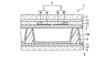
実施の形態1におけるPDPの構造について、図1A〜図1Cを参照して説明する。図1A及び図1Bはそれぞれ、実施の形態1におけるPDPの2つの構成例の一部を示す断面図である。図1Cは、図1Bにおける要部を示す断面図である。
(Embodiment 1)
The structure of the PDP in
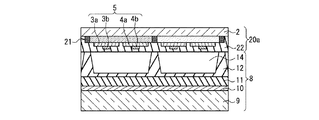
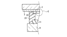
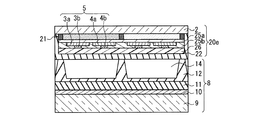
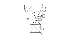
本実施の形態のPDPの基本的な構成について、図1Aを参照して説明する。このPDPでは、前面板20aに、前面側基板2、透明電極3a、4a、バス電極3b、4b、有機顔料からなるカラーフィルタ層21、及び無機コート層22が含まれる。無機コート層22は、カラーフィルタ層21を被覆して形成され、カラーフィルタ層21からの放出ガスの透過を抑制して、放電空間14に入り込むのを阻止する機能を持つ。また、放電時に発生する紫外線によりカラーフィルタ層が変色するのを阻止する機能も持たせることが望ましい。有機顔料からなるカラーフィルタ層を用いると、放電時に発生する紫外線の影響でカラーフィルタ層が変色する場合があるからである。
A basic configuration of the PDP according to the present embodiment will be described with reference to FIG. 1A. In this PDP, the
透明電極3a、4aとバス電極3b、4bは、従来例と同様、走査電極3および維持電極4からなる複数の表示電極対5を構成する。背面板8は、図14〜図15に示した従来例と同様の構造である。背面板8では、背面側基板9上に表示電極対5と立体交差する複数のアドレス電極10が設けられ、アドレス電極10と表示電極対5の交差部には、各々放電セルを形成するための放電空間14を区画する隔壁12が設けられ、隔壁12間に蛍光体層(図示せず。図14〜図15参照)が設けられている。
The
図1Aに示す第1態様の構成では、カラーフィルタ層21は前面側基板2の面上に設けられ、透明電極3a、4aがカラーフィルタ層21上に設けられ、バス電極3b、4bは透明電極3a、4a上に設けられる。従って無機コート層22は、透明電極3a、4a及びバス電極3b、4bを含むカラーフィルタ層21上に設けられている。
In the configuration of the first mode shown in FIG. 1A, the
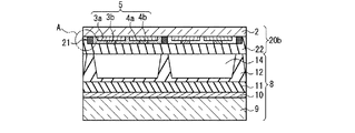
一方、図1Bに示す第2態様の構成では、透明電極3a、4aが前面側基板2の面上に設けられ、バス電極3b、4bが透明電極3a、4a上に設けられ、カラーフィルタ層21が透明電極3a、4a及びバス電極3b、4bを覆って前面側基板2上に設けられる。従って無機コート層22は、カラーフィルタ層21上に設けられている。
On the other hand, in the configuration of the second mode shown in FIG. 1B, the
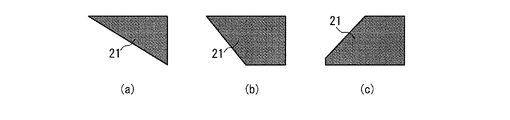
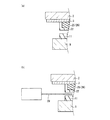
以上のように無機コート層22を設けた構成を採用するためには、図1C(a)に示すように、カラーフィルタ層21の端部(一点鎖線Aで囲った領域)では、なだらかな傾きを持つように形成することが望ましい。この傾きが、図1C(b)のように急峻、あるいは垂直であったり、図1C(c)のように逆の傾きであると、無機コート層22を付設すると応力が発生し割れが発生する場合がある。
In order to employ the configuration in which the
本実施の形態において、カラーフィルタ層21は有機顔料と樹脂を主成分とするが、250℃または300℃までの耐熱性を有する材質を用いることが望ましい。すなわち、無機コート層22(及び後述する保護膜)を、物理気相蒸着、化学気相蒸着またはスパッタリングで成膜できる程度の耐熱性が必要である。
In the present embodiment, the
無機コート層22には、絶縁性があり、可視光を通し易い酸化物(例えば、SiO2、Al2O3、Y2O3、MgO、CaO、SrO等)、窒化物(SiN、SiON、AlN、GaN、BN、InN等)を用い、厚さを数μm程度とする。無機コート層22は、物理気相蒸着,化学気相蒸着、スパッタリング等で成膜することができる。無機コート層22により、カラーフィルタ層21等の有機物から放出するガスが放電空間14に入り込むのを抑制する機能が得られる。
また、無機コート層22は、放電空間14で放電時に放射される紫外線がカラーフィルタ層21等の有機物に当たらないように紫外線をカットする機能も有することが望ましい。例えば、無機コート層22がSiO2の場合、PDPの放電時に発生する紫外線のうち短い波長(147nm)は、無機コート層22で遮断することができる。ただし、PDPの放電時に発生する紫外線のうち長い波長(173nm)は、SiO2の無機コート層22で遮断することは難しい。そこで、SiO2層を形成した後、さらに紫外線が透過しない層を薄く積層してもよい。すなわち、SiO2の場合は、放電による紫外線(173nm)を、保護膜(MgO、CaO、SrO等)を設けることにより遮断することができる。例えば、無機コート層がY2O3の場合、PDPの放電時に発生する紫外線のうち短い波長、長い波長ともに、無機コート層で遮断することができる。
The
In addition, the
カラーフィルタ層21は、各放電空間14の蛍光体層に対応させて配置されている。カラーフィルタ層21の平面形状を図2Aに示す。赤色フィルタ層21r、青色フィルタ層21b、緑色フィルタ層21g、及びブラックストライプ21kからなる。ブラックストライプ21kは、隔壁12に対応させて配置される。また、カラーフィルタ層21の平面形状の他の例を図2Bに示す。赤色フィルタ層21r、青色フィルタ層21b、緑色フィルタ層21g、及びブラックストライプ21kからなる。ブラックストライプ21kは、縦隔壁12のみに対応させて配置される。
The
図1Aの構成における前面板20aを作製するためには、次のような製造方法を用いることができる。まず、前面側基板2に、カラーフィルタ層21をフォトリソグラフィ法、あるいはインクジェット法で形成する。例えばカラーフィルタ層の耐熱温度が250℃であるものとする。次に、透明電極3a、4aを形成する領域に、スパッタ等によってITO膜を形成後(250℃未満の温度)、エッチングにより透明電極3a、4aの電極パターンを形成する。次に、バス電極3b、4bを形成する領域に、スパッタ等によって金属膜(Cr/Cu/Cr等)を形成後(250℃未満の温度)、エッチングによりバス電極3b、4bの電極パターンを形成する。無機コート層22を形成するためには、カラーフィルタ層21が形成された領域を十分覆う範囲に、化学気相蒸着またはスパッタで、SiO2等の膜を形成する(250℃未満の温度)。
In order to produce the
図1Bの構成における前面板20bを作製するためには、次のような製造方法を用いることができる。まず、バス電極3b、4bの作成までは従来と同様のプロセスでよいため、説明を省略する。次に、カラーフィルタ層21をフォトリソグラフィ法、あるいはインクジェット法で形成する。更に、上述の図1Aの構成の場合と同様にして、無機コート層22を形成する。
In order to produce the
以上のように前面板20aあるいは20bを作製した後の、PDP作製のプロセスは、以下のようにすることができる。まず、作成した前面板20aあるいは20bに保護膜(図示せず)を蒸着(250℃未満の温度)した後、大気に暴露することなく、雰囲気を制御した空間で、前面板20aあるいは20bと背面板8とを位置あわせする。
The process for producing the PDP after producing the
次に、雰囲気を制御した空間で背面板8に形成したシールペーストを例えば、レーザー等で局部加熱して、前面板と背面板を封着する。その際、カラーフィルタ層21が形成された領域の温度は250℃未満の温度(基本は常温)に維持する。次に、排気後、ガスを入れて排気管をチップオフする。排気管はあらかじめ背面基板9に接続しておくとよい。
Next, the seal paste formed on the
雰囲気を制御した空間ではない場所、例えば、大気中でパネルの組み立て、封着工程を行うと、保護膜が水酸化する。一般的には排気しながら加熱して、保護膜の水酸化を戻す工程が入る。例えばMgOの場合、300℃以上の温度にする必要がある。 When the panel is assembled and sealed in a place other than the space where the atmosphere is controlled, for example, in the atmosphere, the protective film is hydroxylated. In general, there is a step of heating while exhausting and returning the hydroxylation of the protective film. For example, in the case of MgO, the temperature needs to be 300 ° C. or higher.
本実施の形態では、保護膜蒸着後は、雰囲気を制御した空間でパネル化を行うことにより、保護膜の水酸化を戻す工程が必要なく、250℃未満の温度で工程を行なうことができる。このように、すべての工程で250℃未満の温度で作成することで、カラーフィルタ層21のプロセス劣化なしにPDPを作製することができる。なお、カラーフィルタ層は赤外線を透過しないようにしてもよい。それにより、前面側基板2に赤外線カットフィルタを設けることが不要になる。
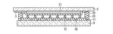
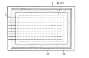
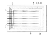
次に、上記構成のPDPの封着構造、すなわち、前面板と背面板をシール層により封着して、両板の間に表示領域を含む放電空間を形成する構造に関する本実施の形態の特徴について説明する。図3は、本実施の形態におけるPDPの封着構造を、前面板の裏面側から示した平面図である。但し、前面板とシール層23の関係のみを明瞭に示すために、背面板は図示が省略されている。図4は、図3に示したPDPの断面図である。この断面図は、図1Aに示した部分断面図とは直交する方向の断面に沿った構造を示すものである。
図3には、各画素セルの放電空間が形成されカラーフィルタ層21が配置された範囲(破線)が、表示領域24として示されている。但し、走査電極3以外の電極は図示が省略されている。また、図4では、表示領域24における走査電極3とカラーフィルタ層21の配置関係の図示を簡略化して、カラーフィルタ層21のみが示されている。
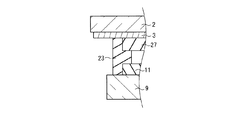
シール層23は、表示領域24を包囲して、前面板20aと背面板8の間(図4参照)の外周縁領域に枠状に設けられて、放電空間を形成している。走査電極3は、表示領域24から放電空間の外部に引き出されている。カラーフィルタ層21を覆って形成された無機コート層22の成膜範囲の外縁は、シール層23と重なる領域内に配置されている。従って、放電空間内では、走査電極3は無機コート層22に覆われている。
この封着構造の要部を、図3のB−B線に沿った断面図として図5に示す。同図の円Cで囲まれた箇所に、放電空間内で、走査電極3が無機コート層22に覆われている状態が示されている。この封止構造により、放電空間内での走査電極3の相互間での放電の発生が抑制される。放電を抑制する効果を得るためには、無機コート層22は、少なくとも走査電極3が配置された領域においては、少なくともシール層23と重なる範囲まで延在して形成されていることが必要である。
なお、上述のとおり封着工程では、シール層23を形成するシールペーストがレーザー等で局部加熱されて溶融する。局部加熱を採用することにより、カラーフィルタ層21については、表示領域24で示されるようにシール層23から離間して配置されているので、封着工程で熱により劣化することが回避される。
図6は、前面板と背面板の封着構造の他の態様を示す前面板の裏面側から見た平面図である。この態様では、無機コート層22の成膜範囲の外縁が、シール層23よりも外方に至っている。無機コート層22にガスバリア性があれば、このような構造を採用することも可能である。
In the present embodiment, after deposition of the protective film, by performing paneling in a space in which the atmosphere is controlled, there is no need to return the hydroxylation of the protective film, and the process can be performed at a temperature of less than 250 ° C. As described above, the PDP can be manufactured without any process deterioration of the
Next, the features of the present embodiment relating to the PDP sealing structure having the above-described structure, that is, the structure in which the front plate and the rear plate are sealed with a sealing layer to form a discharge space including a display area between the two plates will be described. To do. FIG. 3 is a plan view showing the sealing structure of the PDP in the present embodiment from the back side of the front plate. However, in order to clearly show only the relationship between the front plate and the
In FIG. 3, a range (broken line) where the discharge space of each pixel cell is formed and the
The
The principal part of this sealing structure is shown in FIG. 5 as a cross-sectional view along the line BB in FIG. A state surrounded by a circle C in the figure shows a state in which the
As described above, in the sealing step, the seal paste for forming the
FIG. 6 is a plan view seen from the back side of the front plate showing another aspect of the sealing structure of the front plate and the back plate. In this aspect, the outer edge of the film forming range of the
(実施の形態2)
実施の形態2におけるPDPについて、図7A及び図7Bを参照して説明する。図7A及び図7Bはそれぞれ、実施の形態2におけるPDPの2つの構成例の一部を示す断面図である。
(Embodiment 2)
The PDP in
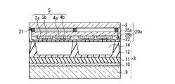
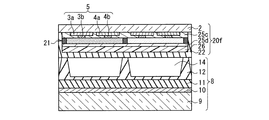
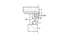
本実施の形態は、実施の形態1の構成に対して、オーバーコート層25a、25bを追加した点が特徴である。オーバーコート層25a、25bは、カラーフィルタ層21の表面を平坦化するために形成される。カラーフィルタ層21の平坦性が悪い(凹凸が大きい)と、カラーフィルタ層21上に透明電極3a、4aを形成し難くなるからである。
The present embodiment is characterized in that overcoat layers 25a and 25b are added to the configuration of the first embodiment. The overcoat layers 25a and 25b are formed to flatten the surface of the
図7Aに示す第1態様の構成は、実施の形態1の図1Aに示した構成に対応する。すなわち、前面板20cでは、カラーフィルタ層21が前面側基板2の面上に設けられ、その上にオーバーコート層25aが形成される。オーバーコート層25aの上に、透明電極3a、4a、及びバス電極3b、4bが順次形成され、その上に、オーバーコート層25bが形成される。従って無機コート層22は、オーバーコート層25b上に設けられている。
The configuration of the first aspect shown in FIG. 7A corresponds to the configuration shown in FIG. 1A of the first embodiment. That is, in the
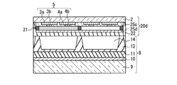
一方、図7Bに示す第2態様の構成は、実施の形態1の図1Bに示した構成に対応する。すなわち、前面板20dでは、透明電極3a、4a及びバス電極3b、4bが前面側基板2の面上に順次形成され、その上にオーバーコート層25cが形成される。オーバーコート層25cの上にカラーフィルタ層21が形成され、その上に、オーバーコート層25dが形成される。従って無機コート層22は、オーバーコート層25d上に設けられている。
On the other hand, the configuration of the second mode illustrated in FIG. 7B corresponds to the configuration illustrated in FIG. 1B of the first embodiment. That is, in the front plate 20d, the
以上のように、オーバーコート層25a〜25dを形成することにより、凹凸を緩和することができる。次のプロセスで完全に凹凸に沿って要素を形成できればよいが、形成できない場合、空間ができることになる。その状態でパネル駆動時に強電界が印加されると、絶縁破壊が発生する。オーバーコート層25a〜25dを設ければ、そのような事態の発生を抑制できる。 As described above, unevenness can be reduced by forming the overcoat layers 25a to 25d. It is sufficient that the element can be completely formed along the unevenness in the next process, but if it cannot be formed, a space is created. In this state, when a strong electric field is applied when driving the panel, dielectric breakdown occurs. If the overcoat layers 25a to 25d are provided, occurrence of such a situation can be suppressed.
オーバーコート層25a〜25dは、アクリル系樹脂、エポキシ系樹脂、ポリイミド系樹脂で形成され、透明である。厚さは2μm程度とする。250℃あるいは300℃の耐熱性を有する。従って、封着シール材の作業温度(例えば470℃程度)には耐えられないので、実施の形態1と同様、局所加熱技術を使って封着する。 The overcoat layers 25a to 25d are formed of an acrylic resin, an epoxy resin, or a polyimide resin and are transparent. The thickness is about 2 μm. It has heat resistance of 250 ° C or 300 ° C. Therefore, since it cannot withstand the working temperature (for example, about 470 ° C.) of the sealing material, sealing is performed using a local heating technique as in the first embodiment.
カラーフィルタ層21の前面のオーバーコート層25a、25dの場合、カラーフィルタ層21と同程度の屈折率にすることで、オーバーコート層25a、25dとカラーフィルタ層21の界面において外光が全反射することを抑制することができる。
In the case of the overcoat layers 25 a and 25 d on the front surface of the
オーバーコート層25a〜25dは、スリットコータ等の印刷装置を用いて形成することができる(250℃未満の温度)。また、本実施の形態の構成によれば、オーバーコート層25a〜25d、カラーフィルタ層21などの有機系の物質を覆う無機コート層22の形成を、それぞれの工程で行わず、一括して行うことで工程の短縮化を図ることができる。
The overcoat layers 25a to 25d can be formed using a printing apparatus such as a slit coater (temperature less than 250 ° C.). Moreover, according to the structure of this Embodiment, formation of the
本実施の形態の構成を有するPDPについても、実施の形態1と同様の封着構造を適用できる。すなわち、オーバーコート層25b、あるいは25dを覆って形成された無機コート層22は、図3に示したものと同様、シール層23と重なる範囲まで延在して形成され、走査電極3を覆っている。それにより、表示領域外の放電空間内での走査電極3の相互間での放電の発生が抑制される。
The same sealing structure as in the first embodiment can also be applied to the PDP having the configuration of the present embodiment. That is, the
(実施の形態3)
実施の形態3におけるPDPについて、図8A及び図8Bを参照して説明する。図8A及び図8Bはそれぞれ、実施の形態3におけるPDPの2つの構成例の一部を示す断面図である。
(Embodiment 3)
The PDP in
本実施の形態は、実施の形態2の構成に対して、有機誘電体層26を追加した点が特徴である。有機誘電体層26は、電極上の誘電体層の厚みを補償して、絶縁耐圧を確保するために形成される。詳細については後述する。
This embodiment is characterized in that an
図8Aに示す第1態様の構成は、実施の形態2の図7Aに示した構成に対応する。すなわち、前面板20eでは、カラーフィルタ層21が前面側基板2の面上に設けられ、その上にオーバーコート層25aが形成される。オーバーコート層25aの上に、透明電極3a、4a、及びバス電極3b、4bが順次形成され、その上に、オーバーコート層25bが形成される。更に、オーバーコート層25b上に有機誘電体層26が形成され、その上に無機コート層22が設けられている。
The configuration of the first aspect shown in FIG. 8A corresponds to the configuration shown in FIG. 7A of the second embodiment. That is, in the
一方、図8Bに示す第2態様の構成は、実施の形態2の図7Bに示した構成に対応する。すなわち、前面板20fでは、透明電極3a、4a及びバス電極3b、4bが前面側基板2の面上に順次形成され、その上にオーバーコート層25cが形成される。オーバーコート層25cの上にカラーフィルタ層21が形成され、その上に、オーバーコート層25dが形成される。更に、オーバーコート層25d上に有機誘電体層26が形成され、その上に無機コート層22が設けられている。
On the other hand, the configuration of the second mode illustrated in FIG. 8B corresponds to the configuration illustrated in FIG. 7B of the second embodiment. That is, in the
なお、図8A、Bでは、有機誘電体層は無機コート層の直下に配置されているが、有機誘電体層とカラーフィルタ層の位置関係を反対にしてもよい。それにより、カラーフィルタ層と発光源を近づけることができる。 8A and 8B, the organic dielectric layer is disposed immediately below the inorganic coat layer, but the positional relationship between the organic dielectric layer and the color filter layer may be reversed. Thereby, the color filter layer and the light emitting source can be brought close to each other.
有機誘電体層26は、アクリル系樹脂、エポキシ系樹脂、あるいはポリイミド系樹脂で形成され、透明である。厚さは10〜20μm程度とする。250℃または300℃程度の耐熱性を有することが望ましい。
The
以下に、有機誘電体層26を設けることによって得られる機能としての、絶縁耐圧の確保について説明する。例えば、実施の形態2における図7Aの第1態様の構造の場合、無機コート層22、オーバーコート層25bが放電空間側の誘電体層の代替要素として機能する。また、図7Bの第2態様の構造の場合は、オーバーコート層25c、25d、カラーフィルタ層21及び無機コート層22が放電空間側の誘電体層の代替要素として機能する。それにより、パネル駆動時に印加される強電界に耐えることができる。
Hereinafter, securing the withstand voltage as a function obtained by providing the
絶縁破壊を起こさないためには、ある一定以上の誘電体層の厚さが必要である。ところが、無機コート層22をスパッタや化学気相蒸着等で形成する場合は、成膜に時間がかかる。一方、カラーフィルタ層21は、色ごとにパターニング形成する必要があり、特に厚いものをフォトレジスト法で形成するのは難しい。また、カラーフィルタ層21を厚くすると、透過率が低下する。従って、カラーフィルタ層21の光学特性を犠牲にすることなく、絶縁破壊が起こらないような厚さの誘電体層を形成することは難しい。むしろ、カラーフィルタ層21は、光学特性を重視して、厚さは色ごとに特性を引き出すのに最適な値にすべきである。
In order not to cause dielectric breakdown, the dielectric layer needs to have a certain thickness or more. However, when the
また、オーバーコート層25b、25c、25dは、電極、カラーフィルタ層21の凹凸を抑制する働きをするので、凹凸に隙間なく入ることが求められる。つまり、オーバーコート層25b、25c、25dの粘度は低いことが望ましい。しかし、粘土の低いものを厚く形成することは難しい。
Moreover, since the overcoat layers 25b, 25c, and 25d function to suppress the unevenness of the electrode and the
誘電体層は更に、放電開始電圧、壁電荷の蓄積量を決める重要な構成要素である。すなわち、放電開始電圧を低くするには、誘電体層の厚さをできるだけ薄くする必要がある。壁電荷の蓄積量は、誘電体層の容量に比例し、誘電体層の容量は、誘電体層の厚さと誘電率で決まる。壁電荷の蓄積量を適切にすることにより、発光効率、輝度、駆動マージンを確保することができる。以上のように、絶縁耐圧を確保するためには誘電体層に最低限の厚さが必要であり、しかも、壁電荷の蓄積量を適切な値にして放電開始電圧ができるだけ低くなるように、誘電体層の厚さを設定する必要がある。 Furthermore, the dielectric layer is an important component that determines the discharge start voltage and the amount of wall charges accumulated. That is, in order to lower the discharge start voltage, it is necessary to make the thickness of the dielectric layer as thin as possible. The amount of wall charge accumulation is proportional to the capacitance of the dielectric layer, and the capacitance of the dielectric layer is determined by the thickness and dielectric constant of the dielectric layer. By making the amount of accumulated wall charges appropriate, light emission efficiency, luminance, and drive margin can be ensured. As described above, in order to ensure the withstand voltage, the dielectric layer needs to have a minimum thickness, and the discharge start voltage is as low as possible by setting the amount of wall charge accumulation to an appropriate value. It is necessary to set the thickness of the dielectric layer.
上述のとおり、無機コート層22、オーバーコート層25b、25c、25d、カラーフィルタ層21については、それぞれの固有の特性を引き出すための材料が決まる。このとき、さらに、厚さ、壁電荷量も考慮して設計する場合、材料の選定幅が狭まるため、それぞれ固有の特性を得難くなる。そこで、有機誘電体層26を導入することで、有機誘電体層によりパネルの壁電荷量および厚さをコントロールすることを可能とする。
As described above, for the
具体的には、無機コート層22、オーバーコート層25b〜25d、カラーフィルタ層21の厚さを薄くし、有機誘電体層26を厚くする。それにより、誘電体の代わりとなる部分の厚さを支配するのは有機誘電体層となる。また、無機コート層22、オーバーコート層25b〜25d、カラーフィルタ層21の厚さを薄くすることにより、それぞれの容量は大きな値になる。有機誘電体層26は、無機コート層22、オーバーコート層25b〜25d、カラーフィルタ層21の厚さよりも厚いので、容量が小さくなる。さらに誘電率も低くすることで、無機コート層22、オーバーコート層25b〜25d、カラーフィルタ層21のそれぞれの容量より小さくすることができる。
Specifically, the
壁電荷量を決めるのは、誘電体の代わりとなる層すべての合成容量である。無機コート層22、オーバーコート層25b〜25d、カラーフィルタ層21、有機誘電体層26の容量はそれぞれ直列に構成されるので、一番容量の小さいものに支配される。つまり、有機誘電体層26に支配される。従って、有機誘電体層26で壁電荷量をコントロールすることができる。特にカラーフィルタの場合、色ごとに材料が異なるので、容量(厚さ、誘電率)が色ごとに異なると、色ごと(放電セルごと)の放電電圧のバラツキが生じやすい。これに対して本実施の形態のように、有機誘電体層により厚さ、壁電荷量をコントロールすることにより、色ごとのバラツキは抑制される。
The wall charge is determined by the combined capacitance of all the layers instead of the dielectric. Since the
実施の形態3では、実施の形態1、2と異なり、有機誘電体層26がある程度の厚さを有することで、絶縁破壊を抑制する。厚さと誘電率を制御することで、壁電荷量をコントロールすることができるので、壁電荷量、絶縁破壊を気にすることなく、カラーフィルタ層21、無機コート層22、オーバーコート層25a〜25dには、それぞれの特性が最も発揮できるような材料を選べばよく、材料選定幅が広がる。
In the third embodiment, unlike the first and second embodiments, the
有機誘電体層26は、スリットコータ等の印刷装置を用いて形成することができる。また、本実施の形態の構成によれば、有機誘電体層26、オーバーコート層25a〜25d、カラーフィルタ層21などの有機系の物質を覆う無機コート層22の形成をそれぞれの工程で行わず、一括して行うことで工程の短縮化をすることができる。
The
本実施の形態の構成を有するPDPについても、実施の形態1と同様の封着構造を適用できる。すなわち、有機誘電体層26を覆って形成された無機コート層22は、図3に示したものと同様、シール層23と重なる範囲まで延在して形成され、走査電極3を覆っている。それにより、表示領域外の放電空間内における走査電極3の相互間での放電の発生が抑制される。
(実施の形態4)
実施の形態4におけるPDPの構成について、図9及び図10Aを参照して説明する。図9は、本実施の形態におけるPDPの封着構造を前面板の裏面側から示した平面図である。図10Aは、この封着構造の要部を示し、図9のD−D線に沿った断面図である。
本実施の形態は、走査電極3の相互間での放電の発生を抑制するための、放電空間内での走査電極3の被覆に、上述の実施の形態における無機コート層22に代えて、あるいは無機コート層22とともに、無機誘電体層27が用いられることを特徴とする。無機誘電体層27を用いるのは、膜厚を確保するためである。無機コート層22は上述のとおり、物理気相蒸着、化学気相蒸着、スパッタリング等成膜される。これらの成膜方法は薄膜を形成する手法であり、数μm程度の膜厚となる。ガスバリア性を有する必要があり、緻密な膜が形成されので、絶縁破壊はし難いものの、もともと膜厚が薄いため、何らかの欠陥等があれば、走査電極に高電圧を印加したときに絶縁破壊を起こす可能性がある。
無機誘電体層27は、シール材23を封着するときに加熱される温度では軟化しないような材料であり、厚膜印刷等で形成する。厚さは例えば、10〜30μm程度であり、例えば現行PDPで使われているものと同じ材料でよい。無機誘電体層27は、十分な厚みが得られるので、走査電極3に高電圧を印加したときに絶縁破壊を起こす可能性が十分に低減される。
無機誘電体層27は、シール層23により前面板と背面板の間に形成された放電空間内において、図9に示すように、少なくともカラーフィルタ層21が配置された表示領域24の外側の領域における走査電極3を覆って形成される。この条件を満足する限り、無機誘電体層27をどのような範囲に形成することもでき、より広範囲の領域に形成してもよい。
また、図10Bに要部を示す他の態様のように、無機コート層22の成膜範囲をその外縁がシール層23の下部領域内に配置されるように設定して、無機コート層22により無機誘電体層27を被覆してもよい。それにより、走査電極3間の放電抑制の信頼性を、より向上させることができる。また、無機誘電体層27はガスバリア性を有していることが望ましい。それにより、実施の形態1の図6に示した無機コート層22のように、シール材23の配置を無機誘電体層27の内側とすることも可能になる。
上記構成のPDPは、以下のような製造工程により作製することができる。前面板の製造工程としては、先ず前面側基板2に、電極を周知の方法により形成する。次に、電極を部分的に覆うように無機誘電体層27を、周知の方法により形成する。無機誘電体層27の凹凸が大きい場合は、実施の形態2で形成したようなオーバーコート層を形成する。更に、各画素に対応させてカラーフィルタ層21をフォトリソグラフィ法、あるいはインクジェット法で形成する。カラーフィルタ層21の凹凸が大きい場合は、オーバーコート層を形成する。
更に、カラーフィルタ層21あるいはオーバーコート層を覆って無機コート層22を形成する。次に、無機コート層22上に保護膜を蒸着する。保護膜蒸着後に、大気に暴露することなく、雰囲気制御された中で、前面板と背面板のアライメントを行い、局所加熱法の一つであるレーザー封着を行う。すなわち、シール層23を形成するためのシール材層が設けられた領域のみ、カラーフィルタ層21、オーバーコート層の耐熱温度より高い温度まで上昇させる。雰囲気制御された空間内で処理を行うため、保護膜を活性化させるために排気時に温度をかける必要もなく、パネル内を排気して、放電ガスを封入する。これらの工程は、実施の形態1で説明したものと同様である。
(実施の形態5)
実施の形態5におけるPDPの構成について、図11及び図12を参照して説明する。図11は、本実施の形態におけるPDPの封着構造を前面板の裏面側から示した平面図である。図12は、この封着構造の要部を示し、図11のE−E線に沿った断面図である。
本実施の形態は、シール層28により形成された放電空間内において走査電極3を覆う層として、オーバーコート層25または有機誘電体層26の少なくとも一方を用いることを特徴とする。すなわち、カラーフィルタ21層及び表示電極対の上部に、オーバーコート25層及び有機誘電体層26の少なくとも一方が設けられ、オーバーコート25層または有機誘電体層26を覆って無機コート層22が形成されている。
少なくとも走査電極3が配置された領域においては、オーバーコート層25または有機誘電体層26の少なくとも一方と無機コート層22とが、シール層28と重なる範囲まで延在して形成されている。実施の形態4における無機誘電体層27と同様、オーバーコート層25または有機誘電体層26は十分な厚みが得られるので、走査電極3に高電圧を印加したときに絶縁破壊を起こす可能性が十分に低減される。
このような構成を可能とするためにシール層28は、オーバーコート層25あるいは有機誘電体層26を実質的に劣化させない温度以下で、低温封着可能な封着シール材により形成される。すなわち、オーバーコート層25、有機誘電体層26の耐熱温度未満での封着が可能であることにより、シール層28の下部までオーバーコート層25、有機誘電体層26を延在させて、膜厚を確保することができる。
低温封着には、封着シール材として例えば、ガラスにはんだ付けが可能な金属はんだ(例えば特許文献3参照)を用いることができる。金属はんだは、例えば、Sn、Cu、In、Bi、Zn、Pb、Sb、Ga、及びAgから成る群から選択された少なくとも1つの材料を含む合金又は金属からなる。さらに、Ti、Al、及びCrから成る群から選択された少なくとも1つの材料を含んでいてもよい。具体的には、Sn−Ag系、Sn−Cu系、Sn−Ag−Cu系、Sn−Ag−Bi系、Sn−Ag−Cu−Bi系等のはんだであって、その共晶点温度が250℃以下となるようなはんだを用いることができる。
実用に供されている金属はんだとしては、溶融温度が、例えば150℃台、180℃台、210℃台、220℃台、240℃台のものがある。これらはオーバーコート層25、有機誘電体層26の耐熱温度未満である。
金属はんだを用いたシール層28による封着は、図13に示すように工程により行なうことができる。まず、実施の形態1〜3で説明したように、前面板と背面板を作製する。次に、図13(a)に示すように、雰囲気制御された空間で前面板と背面板のアライメントを行う。その状態で、図13(b)に示すように、超音波振動機能付きのはんだごて29のこて先を差し込んで、金属はんだを溶融させながら供給する(図示せず)。金属はんだが冷却され固体化して金属はんだ層(図12参照)からなるシール層28が形成されることにより、背面板と前面板間が封着される。
この実施の形態においても、封着時の雰囲気は制御された空間とし、保護膜が水酸化・炭酸化されない状態を維持する。真空引きした後、ガスを封入してチップオフする。チップ管はガラスシールペーストの焼成時に封着させておく。
また、実施の形態1の図6に示した態様のように、シール材28の配置を無機コート層22の内側とすることも可能である。すなわち、オーバーコート層25または有機誘電体層26の少なくとも一方と、無機コート層22とは、その成膜範囲の外縁がシール層28の下部領域よりも外側に延在して配置されている構成としてもよい。
The same sealing structure as in the first embodiment can also be applied to the PDP having the configuration of the present embodiment. That is, the
(Embodiment 4)
The configuration of the PDP in the fourth embodiment will be described with reference to FIGS. 9 and 10A. FIG. 9 is a plan view showing the sealing structure of the PDP in the present embodiment from the back side of the front plate. FIG. 10A shows a main part of the sealing structure, and is a cross-sectional view taken along the line DD of FIG.
In the present embodiment, in order to suppress the occurrence of discharge between the
The
In the discharge space formed between the front plate and the back plate by the
10B, the film formation range of the
The PDP having the above configuration can be manufactured by the following manufacturing process. As a manufacturing process of the front plate, first, electrodes are formed on the
Further, an
(Embodiment 5)
The configuration of the PDP in the fifth embodiment will be described with reference to FIGS. FIG. 11 is a plan view showing the PDP sealing structure in the present embodiment from the back side of the front plate. FIG. 12 is a cross-sectional view taken along the line EE of FIG. 11, showing the main part of this sealing structure.
The present embodiment is characterized in that at least one of the
At least in the region where the
In order to enable such a configuration, the
For low-temperature sealing, for example, metal solder that can be soldered to glass (see, for example, Patent Document 3) can be used as a sealing material. The metal solder is made of, for example, an alloy or metal including at least one material selected from the group consisting of Sn, Cu, In, Bi, Zn, Pb, Sb, Ga, and Ag. Furthermore, at least one material selected from the group consisting of Ti, Al, and Cr may be included. Specifically, it is a solder such as Sn—Ag, Sn—Cu, Sn—Ag—Cu, Sn—Ag—Bi, Sn—Ag—Cu—Bi, and the eutectic point temperature thereof. A solder that is 250 ° C. or lower can be used.
Examples of metal solders that are put into practical use include those having melting temperatures of, for example, 150 ° C., 180 ° C., 210 ° C., 220 ° C., and 240 ° C. These are lower than the heat resistance temperature of the
Sealing with the
Also in this embodiment, the atmosphere during sealing is a controlled space, and the state in which the protective film is not hydroxylated or carbonated is maintained. After evacuation, gas is sealed and the chip is turned off. The tip tube is sealed when the glass seal paste is fired.
Further, as in the aspect shown in FIG. 6 of the first embodiment, the
本発明のPDPは、有機カラーフィルタ層からの放出ガスが放電空間に入り込むことが抑制され、かつ、表示領域外の放電空間における走査電極間での意図しない放電が回避されるので、壁掛けテレビや大型モニターとして有用である。 The PDP of the present invention suppresses the release gas from the organic color filter layer from entering the discharge space and avoids unintentional discharge between the scan electrodes in the discharge space outside the display region. Useful as a large monitor.
1、20a〜20f 前面板
2 前面側基板
3 走査電極
3a、4a 透明電極
3b、4b バス電極
4 維持電極
5 表示電極対
6 前面側誘電体層
7 保護膜
8 背面板
9 背面側基板
10 アドレス電極
11 背面側誘電体層
12 隔壁
12a 縦隔壁
12b 横隔壁
13 蛍光体層
13r 赤色(R)蛍光体層
13g 緑色(G)蛍光体層
13b 青色(B)蛍光体層
14 放電空間
15 放電セル
16 ブラックストライプ
17 誘電体用薄板
18 絶縁被覆膜
19 間隙
21 カラーフィルタ層
22 無機コート層
23、28 シール層
24 表示領域
25、25a〜25d オーバーコート層
26 有機誘電体層
27 無機誘電体層
29 はんだごて
DESCRIPTION OF
Claims (11)
背面側基板上に前記表示電極対と立体交差する複数のアドレス電極が設けられ、前記アドレス電極と前記表示電極対の交差部に各々放電セルを区画する隔壁が設けられ、前記隔壁間に蛍光体層が設けられた背面板と、
前記各放電セルの前記蛍光体層に対応させて前記前面板上に配置され有機顔料を用いて形成されたカラーフィルタ層と、
前記カラーフィルタ層の上部に設けられ、前記カラーフィルタ層からの放出ガスの透過を抑制する無機コート層と、
前記前面板と前記背面板の間の外周縁領域に枠状に設けられ、前記前面板と前記背面板の間を封着しているシール層とを備え、
前記無機コート層は、前記走査電極が配置された領域においては、少なくとも前記シール層と重なる範囲まで延在して形成されていることを特徴とするプラズマディスプレイパネル。 A front plate provided with a plurality of display electrode pairs consisting of scan electrodes and sustain electrodes on a front side substrate;
A plurality of address electrodes that are three-dimensionally crossed with the display electrode pair are provided on a back side substrate, and a partition that partitions discharge cells is provided at the intersection of the address electrode and the display electrode pair, and a phosphor is provided between the partitions. A back plate provided with a layer;
A color filter layer formed on the front plate corresponding to the phosphor layer of each discharge cell and formed using an organic pigment;
An inorganic coating layer that is provided on the color filter layer and suppresses permeation of the released gas from the color filter layer;
Provided in a frame shape in an outer peripheral region between the front plate and the back plate, and a sealing layer sealing between the front plate and the back plate,
The plasma display panel according to claim 1, wherein the inorganic coat layer is formed to extend at least to a range overlapping with the seal layer in a region where the scan electrode is disposed.
背面側基板上に前記表示電極対と立体交差する複数のアドレス電極が設けられ、前記アドレス電極と前記表示電極対の交差部に各々放電セルを区画する隔壁が設けられ、前記隔壁間に蛍光体層が設けられた背面板と、
前記各放電セルの前記蛍光体層に対応させて前記前面板上に配置され有機顔料を用いて形成されたカラーフィルタ層と、
前記カラーフィルタ層の上部に設けられ、前記カラーフィルタ層からの放出ガスの透過を抑制する無機コート層と、
前記前面板と前記背面板の間の外周縁領域に枠状に設けられ、前記前面板と前記背面板の間を封着しているシール層とを備え、
前記シール層により前記前面板と前記背面板の間に形成された放電空間内における、前記走査電極の少なくとも前記カラーフィルタ層が配置された領域の外側に位置する部分を覆って、無機誘電体層が形成されていることを特徴とするプラズマディスプレイパネル。 A front plate provided with a plurality of display electrode pairs consisting of scan electrodes and sustain electrodes on a front side substrate;
A plurality of address electrodes that are three-dimensionally crossed with the display electrode pair are provided on a back side substrate, and a partition that partitions discharge cells is provided at the intersection of the address electrode and the display electrode pair, and a phosphor is provided between the partitions. A back plate provided with a layer;
A color filter layer formed on the front plate corresponding to the phosphor layer of each discharge cell and formed using an organic pigment;
An inorganic coating layer that is provided on the color filter layer and suppresses permeation of the released gas from the color filter layer;
Provided in a frame shape in an outer peripheral region between the front plate and the back plate, and a sealing layer sealing between the front plate and the back plate,
An inorganic dielectric layer is formed to cover at least a portion of the scanning electrode located outside the region where the color filter layer is disposed in the discharge space formed between the front plate and the back plate by the seal layer. A plasma display panel characterized by being made.
背面側基板上に前記表示電極対と立体交差する複数のアドレス電極が設けられ、前記アドレス電極と前記表示電極対の交差部に各々放電セルを区画する隔壁が設けられ、前記隔壁間に蛍光体層が設けられた背面板と、
前記各放電セルの前記蛍光体層に対応させて前記前面板上に配置され有機顔料を用いて形成されたカラーフィルタ層と、
前記カラーフィルタ層の上部に設けられ、前記カラーフィルタ層からの放出ガスの透過を抑制する無機コート層と、
前記前面板と前記背面板の間の外周縁領域に枠状に設けられ、前記前面板と前記背面板の間を封着しているシール層とを備え、
前記カラーフィルタ層及び前記表示電極対の上部に、オーバーコート層及び有機誘電体層の少なくとも一方が設けられ、前記オーバーコート層または有機誘電体層を覆って前記無機コート層が形成され、
少なくとも前記走査電極が配置された領域においては、前記オーバーコート層または前記有機誘電体層の少なくとも一方と前記無機コート層とが、前記シール層と重なる範囲まで延在して形成され、
前記シール層は、前記オーバーコート層または前記有機誘電体層を実質的に劣化させない温度以下で封着可能な封着シール材により形成されていることを特徴とするプラズマディスプレイパネル。 A front plate provided with a plurality of display electrode pairs consisting of scan electrodes and sustain electrodes on a front side substrate;
A plurality of address electrodes that are three-dimensionally crossed with the display electrode pair are provided on a back side substrate, and a partition that partitions discharge cells is provided at the intersection of the address electrode and the display electrode pair, and a phosphor is provided between the partitions. A back plate provided with a layer;
A color filter layer formed on the front plate corresponding to the phosphor layer of each discharge cell and formed using an organic pigment;
An inorganic coating layer that is provided on the color filter layer and suppresses permeation of the released gas from the color filter layer;
Provided in a frame shape in an outer peripheral region between the front plate and the back plate, and a sealing layer sealing between the front plate and the back plate,
At least one of an overcoat layer and an organic dielectric layer is provided on the color filter layer and the display electrode pair, and the inorganic coat layer is formed to cover the overcoat layer or the organic dielectric layer,
At least in the region where the scan electrode is disposed, at least one of the overcoat layer or the organic dielectric layer and the inorganic coat layer are formed to extend to a range overlapping the seal layer,
The plasma display panel, wherein the sealing layer is formed of a sealing material that can be sealed at a temperature or lower that does not substantially deteriorate the overcoat layer or the organic dielectric layer.
Priority Applications (1)
| Application Number | Priority Date | Filing Date | Title |
|---|---|---|---|
| JP2011001292A JP2012142249A (en) | 2011-01-06 | 2011-01-06 | Plasma display panel |
Applications Claiming Priority (1)
| Application Number | Priority Date | Filing Date | Title |
|---|---|---|---|
| JP2011001292A JP2012142249A (en) | 2011-01-06 | 2011-01-06 | Plasma display panel |
Publications (2)
| Publication Number | Publication Date |
|---|---|
| JP2012142249A true JP2012142249A (en) | 2012-07-26 |
| JP2012142249A5 JP2012142249A5 (en) | 2014-01-16 |
Family
ID=46678303
Family Applications (1)
| Application Number | Title | Priority Date | Filing Date |
|---|---|---|---|
| JP2011001292A Pending JP2012142249A (en) | 2011-01-06 | 2011-01-06 | Plasma display panel |
Country Status (1)
| Country | Link |
|---|---|
| JP (1) | JP2012142249A (en) |
Cited By (2)
| Publication number | Priority date | Publication date | Assignee | Title |
|---|---|---|---|---|
| US10033974B2 (en) | 2014-08-29 | 2018-07-24 | Samsung Electronics Co., Ltd. | Electronic device having a color filter and method of forming the same |
| JP2019522905A (en) * | 2016-06-17 | 2019-08-15 | エルジー・ケム・リミテッド | ELECTRODE STRUCTURE, ELECTRONIC DEVICE INCLUDING THE SAME, AND MANUFACTURING METHOD THEREOF |
Citations (7)
| Publication number | Priority date | Publication date | Assignee | Title |
|---|---|---|---|---|
| JPH09283033A (en) * | 1996-04-11 | 1997-10-31 | Hitachi Ltd | Gas discharge type display panel and its manufacture |
| JP2000030617A (en) * | 1998-07-09 | 2000-01-28 | Fujitsu Ltd | Plasma display panel and manufacture of it |
| JP2002341320A (en) * | 2001-05-15 | 2002-11-27 | Fuji Photo Film Co Ltd | Liquid crystal display device and optical laminate |
| JP2004055222A (en) * | 2002-07-17 | 2004-02-19 | Matsushita Electric Ind Co Ltd | Plasma display panel and its manufacturing method |
| JP2007294138A (en) * | 2006-04-21 | 2007-11-08 | Matsushita Electric Ind Co Ltd | Plasma display panel and its manufacturing method |
| JP2008084712A (en) * | 2006-09-28 | 2008-04-10 | Fujitsu Hitachi Plasma Display Ltd | Plasma display panel and manufacturing method of same |
| JP2011044355A (en) * | 2009-08-21 | 2011-03-03 | Advanced Pdp Development Corp | Plasma display panel |
-
2011
- 2011-01-06 JP JP2011001292A patent/JP2012142249A/en active Pending
Patent Citations (7)
| Publication number | Priority date | Publication date | Assignee | Title |
|---|---|---|---|---|
| JPH09283033A (en) * | 1996-04-11 | 1997-10-31 | Hitachi Ltd | Gas discharge type display panel and its manufacture |
| JP2000030617A (en) * | 1998-07-09 | 2000-01-28 | Fujitsu Ltd | Plasma display panel and manufacture of it |
| JP2002341320A (en) * | 2001-05-15 | 2002-11-27 | Fuji Photo Film Co Ltd | Liquid crystal display device and optical laminate |
| JP2004055222A (en) * | 2002-07-17 | 2004-02-19 | Matsushita Electric Ind Co Ltd | Plasma display panel and its manufacturing method |
| JP2007294138A (en) * | 2006-04-21 | 2007-11-08 | Matsushita Electric Ind Co Ltd | Plasma display panel and its manufacturing method |
| JP2008084712A (en) * | 2006-09-28 | 2008-04-10 | Fujitsu Hitachi Plasma Display Ltd | Plasma display panel and manufacturing method of same |
| JP2011044355A (en) * | 2009-08-21 | 2011-03-03 | Advanced Pdp Development Corp | Plasma display panel |
Cited By (3)
| Publication number | Priority date | Publication date | Assignee | Title |
|---|---|---|---|---|
| US10033974B2 (en) | 2014-08-29 | 2018-07-24 | Samsung Electronics Co., Ltd. | Electronic device having a color filter and method of forming the same |
| JP2019522905A (en) * | 2016-06-17 | 2019-08-15 | エルジー・ケム・リミテッド | ELECTRODE STRUCTURE, ELECTRONIC DEVICE INCLUDING THE SAME, AND MANUFACTURING METHOD THEREOF |
| US10749135B2 (en) | 2016-06-17 | 2020-08-18 | Lg Chem, Ltd. | Electrode structure, electronic device comprising same and method for manufacturing same |
Similar Documents
| Publication | Publication Date | Title |
|---|---|---|
| CN100593225C (en) | Electron emission display | |
| KR100884152B1 (en) | Plasma display panel and its manufacturing method | |
| US6803723B1 (en) | Plasma display and method for producing the same | |
| JP2012142249A (en) | Plasma display panel | |
| JP2003338246A (en) | Plasma display device and its manufacturing method | |
| JP3640495B2 (en) | Plasma display panel | |
| CN101160640B (en) | Plasma display panel | |
| JP2011044355A (en) | Plasma display panel | |
| JP2007109479A (en) | Plasma display panel | |
| JP2007184282A (en) | Plasma display panel | |
| JP2005332599A (en) | Plasma display panel and its manufacturing method | |
| JP2003187708A (en) | Plasma display panel | |
| US20080018249A1 (en) | Plasma display panel and production process of same | |
| US7872419B2 (en) | Plasma display panel capable of reducing the defect rate of a dielectric layer and method of manufacturing the same | |
| JP3773517B2 (en) | Plasma display panel | |
| US8681076B2 (en) | Plasma display panel | |
| JP2003208853A (en) | Gas discharge display device and method of manufacturing the device | |
| JP4760178B2 (en) | Plasma display panel | |
| WO2009133622A1 (en) | Method for manufacturing plasma display panel and plasma display panel, and method for manufacturing plasma display device | |
| JP2006031994A (en) | Plasma display panel | |
| JP2008108461A (en) | Plasma display panel | |
| JP2009193947A (en) | Plasma display panel | |
| JP2012064370A (en) | Plasma display panel | |
| KR20080046494A (en) | Plasma display panel | |
| JP2006278146A (en) | Plasma display panel and its manufacturing method |
Legal Events
| Date | Code | Title | Description |
|---|---|---|---|
| A521 | Written amendment |
Free format text: JAPANESE INTERMEDIATE CODE: A523 Effective date: 20131121 |
|
| A621 | Written request for application examination |
Free format text: JAPANESE INTERMEDIATE CODE: A621 Effective date: 20131121 |
|
| A977 | Report on retrieval |
Free format text: JAPANESE INTERMEDIATE CODE: A971007 Effective date: 20140410 |
|
| A131 | Notification of reasons for refusal |
Free format text: JAPANESE INTERMEDIATE CODE: A131 Effective date: 20140417 |
|
| A521 | Written amendment |
Free format text: JAPANESE INTERMEDIATE CODE: A523 Effective date: 20140521 |
|
| A02 | Decision of refusal |
Free format text: JAPANESE INTERMEDIATE CODE: A02 Effective date: 20150305 |