EP3461114B1 - Contact image sensor and image scanning device - Google Patents
Contact image sensor and image scanning device Download PDFInfo
- Publication number
- EP3461114B1 EP3461114B1 EP17798499.4A EP17798499A EP3461114B1 EP 3461114 B1 EP3461114 B1 EP 3461114B1 EP 17798499 A EP17798499 A EP 17798499A EP 3461114 B1 EP3461114 B1 EP 3461114B1
- Authority
- EP
- European Patent Office
- Prior art keywords
- cis
- lens
- light
- original pattern
- scanning device
- Prior art date
- Legal status (The legal status is an assumption and is not a legal conclusion. Google has not performed a legal analysis and makes no representation as to the accuracy of the status listed.)
- Active
Links
- 238000012805 post-processing Methods 0.000 claims description 11
- 239000000758 substrate Substances 0.000 claims description 10
- 238000000034 method Methods 0.000 claims description 7
- 238000012545 processing Methods 0.000 claims description 2
- 238000000701 chemical imaging Methods 0.000 claims 1
- 238000010586 diagram Methods 0.000 description 7
- 230000002708 enhancing effect Effects 0.000 description 4
- 238000003384 imaging method Methods 0.000 description 2
- 238000003491 array Methods 0.000 description 1
- 230000000295 complement effect Effects 0.000 description 1
- 230000000694 effects Effects 0.000 description 1
- 229910044991 metal oxide Inorganic materials 0.000 description 1
- 150000004706 metal oxides Chemical class 0.000 description 1
- 230000003287 optical effect Effects 0.000 description 1
- 239000004065 semiconductor Substances 0.000 description 1
Images


Classifications
-
- H—ELECTRICITY
- H04—ELECTRIC COMMUNICATION TECHNIQUE
- H04N—PICTORIAL COMMUNICATION, e.g. TELEVISION
- H04N1/00—Scanning, transmission or reproduction of documents or the like, e.g. facsimile transmission; Details thereof
- H04N1/024—Details of scanning heads ; Means for illuminating the original
- H04N1/028—Details of scanning heads ; Means for illuminating the original for picture information pick-up
- H04N1/03—Details of scanning heads ; Means for illuminating the original for picture information pick-up with photodetectors arranged in a substantially linear array
- H04N1/031—Details of scanning heads ; Means for illuminating the original for picture information pick-up with photodetectors arranged in a substantially linear array the photodetectors having a one-to-one and optically positive correspondence with the scanned picture elements, e.g. linear contact sensors
-
- G—PHYSICS
- G02—OPTICS
- G02B—OPTICAL ELEMENTS, SYSTEMS OR APPARATUS
- G02B26/00—Optical devices or arrangements for the control of light using movable or deformable optical elements
- G02B26/08—Optical devices or arrangements for the control of light using movable or deformable optical elements for controlling the direction of light
- G02B26/10—Scanning systems
- G02B26/101—Scanning systems with both horizontal and vertical deflecting means, e.g. raster or XY scanners
-
- G—PHYSICS
- G02—OPTICS
- G02B—OPTICAL ELEMENTS, SYSTEMS OR APPARATUS
- G02B3/00—Simple or compound lenses
- G02B3/02—Simple or compound lenses with non-spherical faces
- G02B3/08—Simple or compound lenses with non-spherical faces with discontinuous faces, e.g. Fresnel lens
-
- H—ELECTRICITY
- H04—ELECTRIC COMMUNICATION TECHNIQUE
- H04N—PICTORIAL COMMUNICATION, e.g. TELEVISION
- H04N1/00—Scanning, transmission or reproduction of documents or the like, e.g. facsimile transmission; Details thereof
- H04N1/024—Details of scanning heads ; Means for illuminating the original
- H04N1/028—Details of scanning heads ; Means for illuminating the original for picture information pick-up
- H04N1/03—Details of scanning heads ; Means for illuminating the original for picture information pick-up with photodetectors arranged in a substantially linear array
- H04N1/031—Details of scanning heads ; Means for illuminating the original for picture information pick-up with photodetectors arranged in a substantially linear array the photodetectors having a one-to-one and optically positive correspondence with the scanned picture elements, e.g. linear contact sensors
- H04N1/0314—Details of scanning heads ; Means for illuminating the original for picture information pick-up with photodetectors arranged in a substantially linear array the photodetectors having a one-to-one and optically positive correspondence with the scanned picture elements, e.g. linear contact sensors using photodetectors and illumination means mounted in the same plane on a common support or substrate
-
- H—ELECTRICITY
- H04—ELECTRIC COMMUNICATION TECHNIQUE
- H04N—PICTORIAL COMMUNICATION, e.g. TELEVISION
- H04N1/00—Scanning, transmission or reproduction of documents or the like, e.g. facsimile transmission; Details thereof
- H04N1/04—Scanning arrangements, i.e. arrangements for the displacement of active reading or reproducing elements relative to the original or reproducing medium, or vice versa
- H04N1/0402—Scanning different formats; Scanning with different densities of dots per unit length, e.g. different numbers of dots per inch (dpi); Conversion of scanning standards
- H04N1/042—Details of the method used
- H04N1/0443—Varying the scanning velocity or position
-
- H—ELECTRICITY
- H04—ELECTRIC COMMUNICATION TECHNIQUE
- H04N—PICTORIAL COMMUNICATION, e.g. TELEVISION
- H04N1/00—Scanning, transmission or reproduction of documents or the like, e.g. facsimile transmission; Details thereof
- H04N1/04—Scanning arrangements, i.e. arrangements for the displacement of active reading or reproducing elements relative to the original or reproducing medium, or vice versa
- H04N1/0402—Scanning different formats; Scanning with different densities of dots per unit length, e.g. different numbers of dots per inch (dpi); Conversion of scanning standards
- H04N1/042—Details of the method used
- H04N1/0449—Details of the method used using different sets of scanning elements, e.g. for different formats
- H04N1/0452—Details of the method used using different sets of scanning elements, e.g. for different formats mounted on the same support or substrate
-
- H—ELECTRICITY
- H04—ELECTRIC COMMUNICATION TECHNIQUE
- H04N—PICTORIAL COMMUNICATION, e.g. TELEVISION
- H04N1/00—Scanning, transmission or reproduction of documents or the like, e.g. facsimile transmission; Details thereof
- H04N1/387—Composing, repositioning or otherwise geometrically modifying originals
- H04N1/3877—Image rotation
-
- H—ELECTRICITY
- H04—ELECTRIC COMMUNICATION TECHNIQUE
- H04N—PICTORIAL COMMUNICATION, e.g. TELEVISION
- H04N1/00—Scanning, transmission or reproduction of documents or the like, e.g. facsimile transmission; Details thereof
- H04N1/387—Composing, repositioning or otherwise geometrically modifying originals
- H04N1/393—Enlarging or reducing
- H04N1/3935—Enlarging or reducing with modification of image resolution, i.e. determining the values of picture elements at new relative positions
Definitions
- the present disclosure relates to a field of Contact Image Sensors (CIS), and more particularly to a CIS and an image scanning device, capable of enhancing scanning resolution by utilizing a linear magnifying lens.
- CIS Contact Image Sensors
- the scanning device can be utilized to scan a picture, a file and the like, and then the picture, the file and the like can be input to a computer to be post-edited or stored.
- Scanning resolution is an important index of the scanning device. If the resolution is too low, a scanned image may not meet demands of post-processing.
- the scanning precision of a related scanning device mainly depends on the precision of an optical component.
- the resolution of a Contact Image Sensor depends on the resolution of a photosensitive chip (IC). Illustrated with an IC of 600DPI, a size of a photosensitive window is about 40 ⁇ m. That is to say, the minimum size of a scanned pixel is 40 ⁇ m.
- a method for enhancing the resolution of the photosensitive chip can be utilized. As the resolution of the photosensitive chip is higher, the cost is higher accordingly, and the resolution of the photosensitive chip cannot be enhanced limitlessly.
- a magnifying lens is placed between a scanned object and a scanning module.
- An image magnified entirely is scanned by utilizing a scanning module, so as to increase the scanning resolution.
- this method is disadvantageous in that the size of the whole scanning device is enlarged. For example, if a magnifying factor of the magnifying lens is 5, an image plane of which the minimum size is 500mm and a scanning module of which the minimum length is 500mm are needed in order to scan an object that is 100mm long. This not only increases the size of the scanning device, but also will increase the cost.
- Document CN 102984424 A provides a linear array image reading device which includes a first image sensor capable of reading the whole breadth of a manuscript, and a second image sensor capable of reading a local scope of the manuscript, wherein the two image sensors are connected with each other and can read a focal position of the manuscript.
- Document CN 204856523 U provides an electronic scanning rifle enlargies scanning instrument belongs to electronic scanning rifle field.
- the present disclosure provide two CIS in an image scanning device, in order to enhance scanning resolution
- a CIS includes a frame, a light-transmitting plate, a lens, a photosensitive assembly and a linear magnifying lens, wherein the light-transmitting plate is provided on an upper part of the frame; the frame accommodates the lens; the photosensitive assembly is provided below the lens; and the linear magnifying lens is provided between the light-transmitting plate and the lens, and the linear magnifying lens has a characteristic of linearly magnifying an object in a single direction.
- the photosensitive assembly includes a light-sensing portion and a sensor substrate, wherein the light-sensing portion is configured to receive light converged by the lens, the frame accommodates the sensor substrate, and the sensor substrate is configured to carry photosensitive integrated circuits arranged linearly.
- the linear magnifying lens adopts a linear Fresnel magnifying lens.
- an image scanning device includes a CIS, a pulling mechanism and a control system, wherein the CIS is the CIS provided above; the pulling mechanism is configured to drive the CIS to move; and the control system is configured to control actions of the pulling mechanism and the CIS respectively.
- the image scanning device further includes a post-processing system, configured to process a signal transmitted by the contact image sensor (CIS).
- a post-processing system configured to process a signal transmitted by the contact image sensor (CIS).
- the image scanning device further includes an original pattern table, the original pattern table being configured to place an original pattern.
- the contact image sensor (CIS) includes a first contact image sensor (CIS) and a second contact image sensor (CIS), wherein the first contact image sensor (CIS) is parallel with a first direction, the second contact image sensor (CIS) is parallel with a second direction, and an angle is provided between the first direction and the second direction; and the pulling mechanism includes a first pulling mechanism and a second pulling mechanism, the first pulling mechanism is configured to drive the first contact image sensor (CIS) to move, and the second pulling mechanism is configured to drive the second contact image sensor (CIS) to move.
- the first direction is an X direction
- a second direction is a Y direction.
- a CIS in the related art includes a light source 2, a lens 5, a light-sensing portion 4 receiving light converged by the lens 5, a sensor substrate 3 carrying photosensitive ICs arranged linearly, a frame 1 accommodating the lens 5 and the sensor substrate 3, and a light-transmitting plate 6 provided on an upper part of the frame 1 and configured to carry an original pattern 7.
- the section view of a CIS involved in an embodiment of the present disclosure is as shown in Fig. 2a
- the top view thereof is as shown in Fig. 2b
- the CIS involved in an embodiment of the present disclosure includes a light source 2, a lens 5, a light-sensing portion 4 receiving light converged by the lens 5, a sensor substrate 3 carrying photosensitive ICs arranged linearly, a frame 1 accommodating the lens 5 and the sensor substrate 3, and a light-transmitting plate 6 provided on an upper part of the frame 1 and configured to carry an original pattern 7. All of the above components are identical to those in the related art in structure and working principle, which will not be elaborated herein.
- the CIS involved in some embodiments of the present disclosure further includes a linear Fresnel magnifying lens 8, wherein the linear Fresnel magnifying lens 8 is provided between the light-transmitting plate 6 and the lens 5.
- the linear Fresnel magnifying lens 8 is a lens capable of linearly magnifying an object in a single direction.
- a magnifying factor of the conventional linear Fresnel magnifying lens 8 may reach about 5 times.
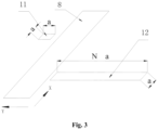
- Fig. 3 shows a magnifying principle diagram of a linear Fresnel magnifying lens involved in an embodiment of the present disclosure.
- a pixel point 11 is taken as an example.
- the pixel point 11 is a pixel point having a length of a in both the X direction and the Y direction
- the magnifying factor of the linear Fresnel magnifying lens 8 is N times, and according to the principle of the linear Fresnel magnifying lens 8, it can be seen that the length a of an image magnified by the linear Fresnel magnifying lens 8 remains unchanged in the X direction and the length in the Y direction will be N times of the original length. That is to say, the length of the image 12 formed by magnifying the pixel point 11 via the linear Fresnel magnifying lens 8 in the X direction is a, and the length in the Y direction is Na.
- Fig. 4 shows a principle diagram of enhancing resolution via a CIS involved in an embodiment of the present disclosure.
- the linear Fresnel magnifying lens 8 is put above the lens 5 of the CIS.
- the distance between the linear Fresnel magnifying lens 8 and the pixel point 11 is an object distance u
- the distance between the linear Fresnel magnifying lens 8 and the image 12 is an image distance v
- the position of the linear Fresnel magnifying lens 8 is properly adjusted, such that the image 12 magnified by the linear Fresnel magnifying lens 8 is located at a focal point of the lens 5, and therefore the image 12 will be converged to the light-sensing portion 4 by the lens 5.
- the lens 5 can converge the image 12 of which the length is a each time, the original pattern 7 moves in the Y direction for a distance of a/N each time, and after the original pattern moves for N times, a pixel point 11 of which the length is a is magnified by the linear Fresnel magnifying lens 8 and can be divided, in the Y direction, into N parts to be scanned.
- resolution in the Y direction can be enhanced by N times, and therefore the novel Contact Image Sensor (CIS) can be utilized to enhance resolution in a single direction.
- CIS Contact Image Sensor
- An image scanning device having the novel CIS can enhance resolution in the X and Y directions, i.e., can enhance the resolution of the whole scanned image. Specific embodiments are adopted for description herein below.
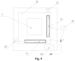
- Fig. 5 shows a structure diagram of an image scanning device as shown in Embodiment 1.
- the image scanning device includes two contact image sensors involved in some embodiments of the present disclosure namely a first CIS X1 and a second CIS Y1.
- the first CIS X1 is parallel with an X direction of the image scanning device
- the second CIS Y1 is parallel with a Y direction of the image scanning device.
- the first CIS X1 is pulled by a first pulling mechanism 21, and the second CIS Y1 is pulled by a second pulling mechanism 22.
- the image scanning device further includes a control system 23, a post-processing system 24 and an original pattern table 25.
- the control system 23 is mainly configured to control normal working of the first CIS X1 and the second CIS Y1, and configured to control actions of the first pulling mechanism 21 and the second pulling mechanism 22.
- the post-processing system 24 is configured to subsequently process signals transmitted by the first CIS X1 and the second CIS Y1.
- the working principle of the image scanning device is as follows. Firstly, an object to be scanned (original pattern 7) is put on the original pattern table 25, light emitted from a light source 2 is irradiated to the original pattern 7 through the original pattern table 25, light reflected by the original pattern 7 enters a linear Fresnel magnifying lens 8 via the original pattern table 25, is magnified, enters a lens 5, and then is converged to a light-sensing portion 4 by the lens 5, and these light signals are converted into electric signals to be output to the post-processing system 24 for subsequent processing.
- the first pulling mechanism 21 pulls the first CIS X1 to move forward in the Y direction at a step of a/N, every time the first CIS X1 moves forward for N steps, a row of pixel points of the original pattern 7 can be scanned, and the light-sensing portion 4 collects N rows of pixel points. Therefore, compared with the related image scanning device, this image scanning device enhances scanning resolution by N times in the Y direction. After scanning is completed, a group of data in the Y direction can be obtained. Likewise, the second pulling mechanism 22 is utilized to pull the second CIS Y1 to perform scanning in the X direction, and a group of data in the X direction can be obtained. The two groups of data are combined into a complete image via the post-processing system 24, a complete image of which the resolution is enhanced by N times can be obtained, and high-resolution scanning is realized.
- the CIS involved in an embodiment of the present disclosure can enhance resolution in a single direction.
- the image scanning device having the CIS involved in the present disclosure can realize high-resolution scanning.
Landscapes
- Engineering & Computer Science (AREA)
- Multimedia (AREA)
- Signal Processing (AREA)
- Physics & Mathematics (AREA)
- General Physics & Mathematics (AREA)
- Optics & Photonics (AREA)
- Facsimile Scanning Arrangements (AREA)
- Facsimile Heads (AREA)
- Image Input (AREA)
Description
- The present disclosure relates to a field of Contact Image Sensors (CIS), and more particularly to a CIS and an image scanning device, capable of enhancing scanning resolution by utilizing a linear magnifying lens.
- With the popularization of computerized office, a scanning device is more and more widely applied. The scanning device can be utilized to scan a picture, a file and the like, and then the picture, the file and the like can be input to a computer to be post-edited or stored. Scanning resolution is an important index of the scanning device. If the resolution is too low, a scanned image may not meet demands of post-processing.
- However, the scanning precision of a related scanning device mainly depends on the precision of an optical component. For example, the resolution of a Contact Image Sensor (CIS) depends on the resolution of a photosensitive chip (IC). Illustrated with an IC of 600DPI, a size of a photosensitive window is about 40µm. That is to say, the minimum size of a scanned pixel is 40µm. To enhance the scanning resolution, a method for enhancing the resolution of the photosensitive chip can be utilized. As the resolution of the photosensitive chip is higher, the cost is higher accordingly, and the resolution of the photosensitive chip cannot be enhanced limitlessly.
- In order to enhance the scanning resolution of the scanning device, some methods have been disclosed in the related art. For example, a magnifying lens is placed between a scanned object and a scanning module. An image magnified entirely is scanned by utilizing a scanning module, so as to increase the scanning resolution. However, this method is disadvantageous in that the size of the whole scanning device is enlarged. For example, if a magnifying factor of the magnifying lens is 5, an image plane of which the minimum size is 500mm and a scanning module of which the minimum length is 500mm are needed in order to scan an object that is 100mm long. This not only increases the size of the scanning device, but also will increase the cost.
- Document
US 6288779 B1 provides a close-up imaging device which takes advantage of the pinhole effect that is achieved with complementary metal oxide semiconductor imaging arrays. - Document
CN 102984424 A provides a linear array image reading device which includes a first image sensor capable of reading the whole breadth of a manuscript, and a second image sensor capable of reading a local scope of the manuscript, wherein the two image sensors are connected with each other and can read a focal position of the manuscript. - Document
CN 204856523 U provides an electronic scanning rifle enlargies scanning instrument belongs to electronic scanning rifle field. - The invention is defined by the appended set of claims.
- In order to solve the problem in the related art, the present disclosure provide two CIS in an image scanning device, in order to enhance scanning resolution
-
-
Fig. 1 shows a section view of a CIS in the related art; -
Fig. 2a shows a section view of a CIS involved in an embodiment of the present disclosure; -
Fig. 2b shows a top view of a CIS involved in an embodiment of the present disclosure; -
Fig. 3 shows a magnifying principle diagram of a linear Fresnel magnifying lens involved in an embodiment of the present disclosure; -
Fig. 4 shows a principle diagram of enhancing resolution via a CIS involved in an embodiment of the present disclosure; -
Fig. 5 shows a structure diagram of an image scanning device as shown inEmbodiment 1; and -
Fig. 6 shows a structure diagram of an image scanning device not covered by the scope of claims. - Drawing marks: 1: frame; 2: light source; 3: sensor substrate; 4: light-sensing portion; 5: lens; 6: light-transmitting plate; 7: original pattern; 8: linear Fresnel magnifying lens; 11: pixel point; 12: image; 21: first pulling mechanism; 22: second pulling mechanism; 23: control system; 24: post-processing system; 25: original pattern table; u: object distance; v: image distance; X1: first CIS; and Y1: second CIS.
- According to the present disclosure, a CIS is provided. The CIS includes a frame, a light-transmitting plate, a lens, a photosensitive assembly and a linear magnifying lens, wherein the light-transmitting plate is provided on an upper part of the frame; the frame accommodates the lens; the photosensitive assembly is provided below the lens; and the linear magnifying lens is provided between the light-transmitting plate and the lens, and the linear magnifying lens has a characteristic of linearly magnifying an object in a single direction.
- In an exemplary embodiment, the photosensitive assembly includes a light-sensing portion and a sensor substrate, wherein the light-sensing portion is configured to receive light converged by the lens, the frame accommodates the sensor substrate, and the sensor substrate is configured to carry photosensitive integrated circuits arranged linearly.
- In an exemplary embodiment, the linear magnifying lens adopts a linear Fresnel magnifying lens.
- According to some embodiments of the present disclosure, an image scanning device is provided. The image scanning device includes a CIS, a pulling mechanism and a control system, wherein the CIS is the CIS provided above; the pulling mechanism is configured to drive the CIS to move; and the control system is configured to control actions of the pulling mechanism and the CIS respectively.
- In an exemplary embodiment, the image scanning device further includes a post-processing system, configured to process a signal transmitted by the contact image sensor (CIS).
- In an exemplary embodiment, the image scanning device further includes an original pattern table, the original pattern table being configured to place an original pattern.
- In an exemplary embodiment, the contact image sensor (CIS) includes a first contact image sensor (CIS) and a second contact image sensor (CIS), wherein the first contact image sensor (CIS) is parallel with a first direction, the second contact image sensor (CIS) is parallel with a second direction, and an angle is provided between the first direction and the second direction; and the pulling mechanism includes a first pulling mechanism and a second pulling mechanism, the first pulling mechanism is configured to drive the first contact image sensor (CIS) to move, and the second pulling mechanism is configured to drive the second contact image sensor (CIS) to move. Specifically, as a first specific embodiment of the present disclosure, as shown in
Fig. 3 , the first direction is an X direction, and a second direction is a Y direction. - The embodiments of the present disclosure will be further described herein below in conjunction with the drawings.
- As shown in
Fig. 1 , a CIS in the related art includes alight source 2, alens 5, a light-sensingportion 4 receiving light converged by thelens 5, asensor substrate 3 carrying photosensitive ICs arranged linearly, aframe 1 accommodating thelens 5 and thesensor substrate 3, and a light-transmittingplate 6 provided on an upper part of theframe 1 and configured to carry anoriginal pattern 7. - The section view of a CIS involved in an embodiment of the present disclosure is as shown in
Fig. 2a , and the top view thereof is as shown inFig. 2b . From the figures, it can be seen that the CIS involved in an embodiment of the present disclosure includes alight source 2, alens 5, a light-sensingportion 4 receiving light converged by thelens 5, asensor substrate 3 carrying photosensitive ICs arranged linearly, aframe 1 accommodating thelens 5 and thesensor substrate 3, and a light-transmittingplate 6 provided on an upper part of theframe 1 and configured to carry anoriginal pattern 7. All of the above components are identical to those in the related art in structure and working principle, which will not be elaborated herein. The CIS involved in some embodiments of the present disclosure further includes a linear Fresnelmagnifying lens 8, wherein the linear Fresnelmagnifying lens 8 is provided between the light-transmittingplate 6 and thelens 5. - The linear Fresnel
magnifying lens 8 is a lens capable of linearly magnifying an object in a single direction. A magnifying factor of the conventional linear Fresnelmagnifying lens 8 may reach about 5 times.Fig. 3 shows a magnifying principle diagram of a linear Fresnel magnifying lens involved in an embodiment of the present disclosure. Apixel point 11 is taken as an example. Thepixel point 11 is a pixel point having a length of a in both the X direction and the Y direction, the magnifying factor of the linear Fresnelmagnifying lens 8 is N times, and according to the principle of the linear Fresnelmagnifying lens 8, it can be seen that the length a of an image magnified by the linear Fresnelmagnifying lens 8 remains unchanged in the X direction and the length in the Y direction will be N times of the original length. That is to say, the length of theimage 12 formed by magnifying thepixel point 11 via the linear Fresnelmagnifying lens 8 in the X direction is a, and the length in the Y direction is Na. Thus, light emitted from thelight source 2 is emitted to theoriginal pattern 7, and light reflected by theoriginal pattern 7 enters the linear Fresnelmagnifying lens 8, is magnified to be N times larger in the Y direction by the linear Fresnelmagnifying lens 8, enters thelens 5, and then is converged on the light-sensingportion 4. Other subsequent processes are basically the same as those in the related art, and will not be elaborated herein. -
Fig. 4 shows a principle diagram of enhancing resolution via a CIS involved in an embodiment of the present disclosure. The linear Fresnelmagnifying lens 8 is put above thelens 5 of the CIS. The distance between the linearFresnel magnifying lens 8 and thepixel point 11 is an object distance u, the distance between the linearFresnel magnifying lens 8 and theimage 12 is an image distance v, and the position of the linearFresnel magnifying lens 8 is properly adjusted, such that theimage 12 magnified by the linearFresnel magnifying lens 8 is located at a focal point of thelens 5, and therefore theimage 12 will be converged to the light-sensingportion 4 by thelens 5. Certainly, thelens 5 can converge theimage 12 of which the length is a each time, theoriginal pattern 7 moves in the Y direction for a distance of a/N each time, and after the original pattern moves for N times, apixel point 11 of which the length is a is magnified by the linearFresnel magnifying lens 8 and can be divided, in the Y direction, into N parts to be scanned. Thus, resolution in the Y direction can be enhanced by N times, and therefore the novel Contact Image Sensor (CIS) can be utilized to enhance resolution in a single direction. - An image scanning device having the novel CIS can enhance resolution in the X and Y directions, i.e., can enhance the resolution of the whole scanned image. Specific embodiments are adopted for description herein below.
-
Fig. 5 shows a structure diagram of an image scanning device as shown inEmbodiment 1. The main difference between the image scanning device and a conventional image scanning device lies in that: the image scanning device includes two contact image sensors involved in some embodiments of the present disclosure namely a first CIS X1 and a second CIS Y1. The first CIS X1 is parallel with an X direction of the image scanning device, and the second CIS Y1 is parallel with a Y direction of the image scanning device. The first CIS X1 is pulled by a first pullingmechanism 21, and the second CIS Y1 is pulled by a second pullingmechanism 22. The image scanning device further includes acontrol system 23, apost-processing system 24 and an original pattern table 25. Thecontrol system 23 is mainly configured to control normal working of the first CIS X1 and the second CIS Y1, and configured to control actions of the first pullingmechanism 21 and the second pullingmechanism 22. Thepost-processing system 24 is configured to subsequently process signals transmitted by the first CIS X1 and the second CIS Y1. - The working principle of the image scanning device is as follows. Firstly, an object to be scanned (original pattern 7) is put on the original pattern table 25, light emitted from a
light source 2 is irradiated to theoriginal pattern 7 through the original pattern table 25, light reflected by theoriginal pattern 7 enters a linearFresnel magnifying lens 8 via the original pattern table 25, is magnified, enters alens 5, and then is converged to a light-sensingportion 4 by thelens 5, and these light signals are converted into electric signals to be output to thepost-processing system 24 for subsequent processing. Under the control of thecontrol system 23, the first pullingmechanism 21 pulls the first CIS X1 to move forward in the Y direction at a step of a/N, every time the first CIS X1 moves forward for N steps, a row of pixel points of theoriginal pattern 7 can be scanned, and the light-sensingportion 4 collects N rows of pixel points. Therefore, compared with the related image scanning device, this image scanning device enhances scanning resolution by N times in the Y direction. After scanning is completed, a group of data in the Y direction can be obtained. Likewise, the second pullingmechanism 22 is utilized to pull the second CIS Y1 to perform scanning in the X direction, and a group of data in the X direction can be obtained. The two groups of data are combined into a complete image via thepost-processing system 24, a complete image of which the resolution is enhanced by N times can be obtained, and high-resolution scanning is realized. - The CIS involved in an embodiment of the present disclosure can enhance resolution in a single direction. The image scanning device having the CIS involved in the present disclosure can realize high-resolution scanning.
Claims (1)
- An image scanning device comprising a Contact Image Sensor, CIS, the image scanning device comprising two CISs, the first CIS (X1) being parallel with an X direction of the image scanning device, the second CIS (Y1) being parallel with a Y direction of the image scanning device, the first CIS (X1) being pulled by a first pulling mechanism (21), the second CIS (Y1) being pulled by a second pulling mechanism (22), the image scanning device further comprising a control system (23), a post-processing system (24) and an original pattern table (25), wherein the control system (23) is configured to control normal working of the first CIS (X1) and the second CIS (Y1), and configured to control actions of the first pulling mechanism (21) and the second pulling mechanism (22); and the post-processing system (24) is configured to process signals transmitted by the first CIS (X1) and the second CIS (Y1), and the original pattern table (25) is configured to place an original pattern; wherein the Contact Image Sensor comprises a light source (2), a lens (5), a light-sensing portion (4) receiving light converged by the lens (5), a sensor substrate (3) carrying photosensitive Integrated Circuits, IC, arranged linearly, a frame (1) accommodating the lens (5) and the sensor substrate (3), and a light-transmitting plate (6) provided on an upper part of the frame (1), wherein the CIS further comprises a linear: Fresnel magnifying lens (8), the linear: Fresnel magnifying lens (8) being provided between the light-transmitting plate (6) and the lens (5), and the linear Fresnel magnifying lens (8) having a characteristic of linearly magnifying an object in a single direction;
wherein:light emitted from the light source (2) is irradiated to the original pattern (7) through the original pattern table (25), light reflected by the original pattern (7) enters the linear Fresnel magnifying lens (8) via the original pattern table (25), is magnified, enters the lens (5), and then is converged to the light-sensing portion (4) by the lens (5), and these light signals are converted into electric signals to be output to the post-processing system (24) for subsequent processing;under the control of the control system (23), the first pulling mechanism (21) pulls the first CIS (X1) to move forward in the Y direction at a step of a/N, every time the first CIS X1 moves forward for N steps, a row of pixel points of the original pattern (7) can be scanned, and the light-sensing portion (4) collects N rows of pixel points, after scanning is completed, a group of data in the Y direction can be obtained; the second pulling mechanism (22) is utilized to pull the second CIS (Y1) to perform scanning in the X direction, and a group of data in the X direction can be obtained; a is a length of a pixel point to be magnified via the linear magnifying lens in the X direction or the Y direction;the two groups of data are combined into a complete image via the post-processing system (24).
Applications Claiming Priority (2)
| Application Number | Priority Date | Filing Date | Title |
|---|---|---|---|
| CN201610330199.3A CN105872292B (en) | 2016-05-18 | 2016-05-18 | A kind of contact-type image sensor and image-scanning device |
| PCT/CN2017/073235 WO2017197930A1 (en) | 2016-05-18 | 2017-02-10 | Contact image sensor and image scanning device |
Publications (3)
| Publication Number | Publication Date |
|---|---|
| EP3461114A1 EP3461114A1 (en) | 2019-03-27 |
| EP3461114A4 EP3461114A4 (en) | 2020-01-08 |
| EP3461114B1 true EP3461114B1 (en) | 2023-03-22 |
Family
ID=56634344
Family Applications (1)
| Application Number | Title | Priority Date | Filing Date |
|---|---|---|---|
| EP17798499.4A Active EP3461114B1 (en) | 2016-05-18 | 2017-02-10 | Contact image sensor and image scanning device |
Country Status (5)
| Country | Link |
|---|---|
| US (1) | US10911629B2 (en) |
| EP (1) | EP3461114B1 (en) |
| JP (1) | JP6664496B2 (en) |
| CN (1) | CN105872292B (en) |
| WO (1) | WO2017197930A1 (en) |
Families Citing this family (3)
| Publication number | Priority date | Publication date | Assignee | Title |
|---|---|---|---|---|
| CN105872292B (en) * | 2016-05-18 | 2019-02-19 | 威海华菱光电股份有限公司 | A kind of contact-type image sensor and image-scanning device |
| CN106303145A (en) * | 2016-09-28 | 2017-01-04 | 威海华菱光电股份有限公司 | Image read-out |
| CN108489548A (en) * | 2018-04-11 | 2018-09-04 | 广东理工学院 | Plank detecting system |
Family Cites Families (13)
| Publication number | Priority date | Publication date | Assignee | Title |
|---|---|---|---|---|
| JPS62142461A (en) | 1985-12-17 | 1987-06-25 | Matsushita Electric Ind Co Ltd | Solid-state image pickup device |
| JPH11164093A (en) * | 1997-12-01 | 1999-06-18 | Ricoh Co Ltd | Image reader |
| US6288779B1 (en) * | 1999-03-24 | 2001-09-11 | Intel Corporation | Close-up imaging device using a CMOS photosensitive element |
| CN2559995Y (en) * | 2002-08-27 | 2003-07-09 | 阮立山 | Ultrathin Fresnel hand lens |
| US7327513B2 (en) * | 2003-05-28 | 2008-02-05 | The Regents Of The University Of California | Method and apparatus for viewing target |
| CN201060321Y (en) * | 2007-05-26 | 2008-05-14 | 钱文耀 | Dual-magnification card type magnifier |
| JP2009206842A (en) * | 2008-02-28 | 2009-09-10 | Panasonic Corp | Image reader |
| JP4511608B2 (en) * | 2008-03-21 | 2010-07-28 | シャープ株式会社 | Document reader |
| JP2013037298A (en) * | 2011-08-10 | 2013-02-21 | Nippon Sheet Glass Co Ltd | Erecting life-size lens array plate |
| CN102984424B (en) * | 2012-12-18 | 2014-12-10 | 威海华菱光电股份有限公司 | Contact image sensor |
| CN204856523U (en) * | 2015-09-06 | 2015-12-09 | 浪潮电子信息产业股份有限公司 | Electronic scanning rifle enlarges scanning instrument |
| CN105872292B (en) * | 2016-05-18 | 2019-02-19 | 威海华菱光电股份有限公司 | A kind of contact-type image sensor and image-scanning device |
| CN205647681U (en) * | 2016-05-18 | 2016-10-12 | 威海华菱光电股份有限公司 | Contact -type image sensor and image scanning device |
-
2016
- 2016-05-18 CN CN201610330199.3A patent/CN105872292B/en active Active
-
2017
- 2017-02-10 JP JP2018535356A patent/JP6664496B2/en active Active
- 2017-02-10 EP EP17798499.4A patent/EP3461114B1/en active Active
- 2017-02-10 WO PCT/CN2017/073235 patent/WO2017197930A1/en unknown
- 2017-02-10 US US16/099,442 patent/US10911629B2/en active Active
Also Published As
| Publication number | Publication date |
|---|---|
| CN105872292A (en) | 2016-08-17 |
| EP3461114A1 (en) | 2019-03-27 |
| EP3461114A4 (en) | 2020-01-08 |
| CN105872292B (en) | 2019-02-19 |
| JP2019506061A (en) | 2019-02-28 |
| US20190149686A1 (en) | 2019-05-16 |
| US10911629B2 (en) | 2021-02-02 |
| WO2017197930A1 (en) | 2017-11-23 |
| JP6664496B2 (en) | 2020-03-13 |
Similar Documents
| Publication | Publication Date | Title |
|---|---|---|
| EP3461114B1 (en) | Contact image sensor and image scanning device | |
| JPS58225773A (en) | Method and device for reading color picture | |
| US20080231915A1 (en) | Scanning device with multifocus and multiresolution | |
| CN108802961A (en) | Focus detection and imaging system | |
| US11374041B2 (en) | Systems and methods for imaging using mechanical scanning mechanisms | |
| US20100027869A1 (en) | Optical Carriage Structure of Inspection Apparatus and its Inspection Method | |
| CN205647681U (en) | Contact -type image sensor and image scanning device | |
| JPH0730716A (en) | Original reader | |
| JP2004126284A (en) | Image read unit and image reader | |
| JP2022532705A (en) | Fingerprint sensor, fingerprint module and terminal equipment | |
| JP2000134414A (en) | Optical scanner | |
| TWI580018B (en) | Wafer-level lens for contact type image sensor | |
| TW583875B (en) | Image devices using multiple linear image sensor arrays | |
| US20100277773A1 (en) | Penta-mirror multi-reflection scanning module | |
| JPH03295354A (en) | Picture reader | |
| CN101609511B (en) | Imaging device and detection method for exposure image | |
| USRE42710E1 (en) | Apparatus compensating a scanned object for optical characteristics according to light sources of different wavelengths | |
| CN1194528C (en) | Scanning method and device with raised resolution | |
| TWI282620B (en) | Contact type image sensor module and the sensing substrate | |
| CN1191980A (en) | Optical waveguide reduction optical image sensor | |
| JP3642692B2 (en) | Image reading device | |
| JP3160906B2 (en) | Film image reader | |
| US20110019247A1 (en) | Imaging system and method | |
| US6392774B1 (en) | Multiple position guiding lens image scanning method | |
| JP2002290683A (en) | Operation-synchronized two-dimensional rectilinear image sensor array |
Legal Events
| Date | Code | Title | Description |
|---|---|---|---|
| STAA | Information on the status of an ep patent application or granted ep patent |
Free format text: STATUS: THE INTERNATIONAL PUBLICATION HAS BEEN MADE |
|
| PUAI | Public reference made under article 153(3) epc to a published international application that has entered the european phase |
Free format text: ORIGINAL CODE: 0009012 |
|
| STAA | Information on the status of an ep patent application or granted ep patent |
Free format text: STATUS: REQUEST FOR EXAMINATION WAS MADE |
|
| 17P | Request for examination filed |
Effective date: 20181120 |
|
| AK | Designated contracting states |
Kind code of ref document: A1 Designated state(s): AL AT BE BG CH CY CZ DE DK EE ES FI FR GB GR HR HU IE IS IT LI LT LU LV MC MK MT NL NO PL PT RO RS SE SI SK SM TR |
|
| AX | Request for extension of the european patent |
Extension state: BA ME |
|
| STAA | Information on the status of an ep patent application or granted ep patent |
Free format text: STATUS: REQUEST FOR EXAMINATION WAS MADE |
|
| DAV | Request for validation of the european patent (deleted) | ||
| DAX | Request for extension of the european patent (deleted) | ||
| A4 | Supplementary search report drawn up and despatched |
Effective date: 20191210 |
|
| RIC1 | Information provided on ipc code assigned before grant |
Ipc: H04N 1/04 20060101ALI20191204BHEP Ipc: H04N 1/031 20060101AFI20191204BHEP Ipc: H04N 1/387 20060101ALI20191204BHEP Ipc: G02B 26/10 20060101ALI20191204BHEP |
|
| STAA | Information on the status of an ep patent application or granted ep patent |
Free format text: STATUS: EXAMINATION IS IN PROGRESS |
|
| 17Q | First examination report despatched |
Effective date: 20210720 |
|
| STAA | Information on the status of an ep patent application or granted ep patent |
Free format text: STATUS: EXAMINATION IS IN PROGRESS |
|
| GRAP | Despatch of communication of intention to grant a patent |
Free format text: ORIGINAL CODE: EPIDOSNIGR1 |
|
| STAA | Information on the status of an ep patent application or granted ep patent |
Free format text: STATUS: GRANT OF PATENT IS INTENDED |
|
| INTG | Intention to grant announced |
Effective date: 20221125 |
|
| GRAS | Grant fee paid |
Free format text: ORIGINAL CODE: EPIDOSNIGR3 |
|
| GRAA | (expected) grant |
Free format text: ORIGINAL CODE: 0009210 |
|
| STAA | Information on the status of an ep patent application or granted ep patent |
Free format text: STATUS: THE PATENT HAS BEEN GRANTED |
|
| AK | Designated contracting states |
Kind code of ref document: B1 Designated state(s): AL AT BE BG CH CY CZ DE DK EE ES FI FR GB GR HR HU IE IS IT LI LT LU LV MC MK MT NL NO PL PT RO RS SE SI SK SM TR |
|
| REG | Reference to a national code |
Ref country code: GB Ref legal event code: FG4D |
|
| REG | Reference to a national code |
Ref country code: CH Ref legal event code: EP |
|
| REG | Reference to a national code |
Ref country code: IE Ref legal event code: FG4D |
|
| REG | Reference to a national code |
Ref country code: DE Ref legal event code: R096 Ref document number: 602017067039 Country of ref document: DE |
|
| REG | Reference to a national code |
Ref country code: AT Ref legal event code: REF Ref document number: 1555957 Country of ref document: AT Kind code of ref document: T Effective date: 20230415 |
|
| REG | Reference to a national code |
Ref country code: LT Ref legal event code: MG9D |
|
| REG | Reference to a national code |
Ref country code: NL Ref legal event code: MP Effective date: 20230322 |
|
| PG25 | Lapsed in a contracting state [announced via postgrant information from national office to epo] |
Ref country code: RS Free format text: LAPSE BECAUSE OF FAILURE TO SUBMIT A TRANSLATION OF THE DESCRIPTION OR TO PAY THE FEE WITHIN THE PRESCRIBED TIME-LIMIT Effective date: 20230322 Ref country code: NO Free format text: LAPSE BECAUSE OF FAILURE TO SUBMIT A TRANSLATION OF THE DESCRIPTION OR TO PAY THE FEE WITHIN THE PRESCRIBED TIME-LIMIT Effective date: 20230622 Ref country code: LV Free format text: LAPSE BECAUSE OF FAILURE TO SUBMIT A TRANSLATION OF THE DESCRIPTION OR TO PAY THE FEE WITHIN THE PRESCRIBED TIME-LIMIT Effective date: 20230322 Ref country code: LT Free format text: LAPSE BECAUSE OF FAILURE TO SUBMIT A TRANSLATION OF THE DESCRIPTION OR TO PAY THE FEE WITHIN THE PRESCRIBED TIME-LIMIT Effective date: 20230322 Ref country code: HR Free format text: LAPSE BECAUSE OF FAILURE TO SUBMIT A TRANSLATION OF THE DESCRIPTION OR TO PAY THE FEE WITHIN THE PRESCRIBED TIME-LIMIT Effective date: 20230322 |
|
| REG | Reference to a national code |
Ref country code: AT Ref legal event code: MK05 Ref document number: 1555957 Country of ref document: AT Kind code of ref document: T Effective date: 20230322 |
|
| PG25 | Lapsed in a contracting state [announced via postgrant information from national office to epo] |
Ref country code: SE Free format text: LAPSE BECAUSE OF FAILURE TO SUBMIT A TRANSLATION OF THE DESCRIPTION OR TO PAY THE FEE WITHIN THE PRESCRIBED TIME-LIMIT Effective date: 20230322 Ref country code: NL Free format text: LAPSE BECAUSE OF FAILURE TO SUBMIT A TRANSLATION OF THE DESCRIPTION OR TO PAY THE FEE WITHIN THE PRESCRIBED TIME-LIMIT Effective date: 20230322 Ref country code: GR Free format text: LAPSE BECAUSE OF FAILURE TO SUBMIT A TRANSLATION OF THE DESCRIPTION OR TO PAY THE FEE WITHIN THE PRESCRIBED TIME-LIMIT Effective date: 20230623 Ref country code: FI Free format text: LAPSE BECAUSE OF FAILURE TO SUBMIT A TRANSLATION OF THE DESCRIPTION OR TO PAY THE FEE WITHIN THE PRESCRIBED TIME-LIMIT Effective date: 20230322 |
|
| PG25 | Lapsed in a contracting state [announced via postgrant information from national office to epo] |
Ref country code: SM Free format text: LAPSE BECAUSE OF FAILURE TO SUBMIT A TRANSLATION OF THE DESCRIPTION OR TO PAY THE FEE WITHIN THE PRESCRIBED TIME-LIMIT Effective date: 20230322 Ref country code: RO Free format text: LAPSE BECAUSE OF FAILURE TO SUBMIT A TRANSLATION OF THE DESCRIPTION OR TO PAY THE FEE WITHIN THE PRESCRIBED TIME-LIMIT Effective date: 20230322 Ref country code: PT Free format text: LAPSE BECAUSE OF FAILURE TO SUBMIT A TRANSLATION OF THE DESCRIPTION OR TO PAY THE FEE WITHIN THE PRESCRIBED TIME-LIMIT Effective date: 20230724 Ref country code: ES Free format text: LAPSE BECAUSE OF FAILURE TO SUBMIT A TRANSLATION OF THE DESCRIPTION OR TO PAY THE FEE WITHIN THE PRESCRIBED TIME-LIMIT Effective date: 20230322 Ref country code: EE Free format text: LAPSE BECAUSE OF FAILURE TO SUBMIT A TRANSLATION OF THE DESCRIPTION OR TO PAY THE FEE WITHIN THE PRESCRIBED TIME-LIMIT Effective date: 20230322 Ref country code: AT Free format text: LAPSE BECAUSE OF FAILURE TO SUBMIT A TRANSLATION OF THE DESCRIPTION OR TO PAY THE FEE WITHIN THE PRESCRIBED TIME-LIMIT Effective date: 20230322 |
|
| PG25 | Lapsed in a contracting state [announced via postgrant information from national office to epo] |
Ref country code: SK Free format text: LAPSE BECAUSE OF FAILURE TO SUBMIT A TRANSLATION OF THE DESCRIPTION OR TO PAY THE FEE WITHIN THE PRESCRIBED TIME-LIMIT Effective date: 20230322 Ref country code: PL Free format text: LAPSE BECAUSE OF FAILURE TO SUBMIT A TRANSLATION OF THE DESCRIPTION OR TO PAY THE FEE WITHIN THE PRESCRIBED TIME-LIMIT Effective date: 20230322 Ref country code: IS Free format text: LAPSE BECAUSE OF FAILURE TO SUBMIT A TRANSLATION OF THE DESCRIPTION OR TO PAY THE FEE WITHIN THE PRESCRIBED TIME-LIMIT Effective date: 20230722 |
|
| REG | Reference to a national code |
Ref country code: DE Ref legal event code: R097 Ref document number: 602017067039 Country of ref document: DE |
|
| PLBE | No opposition filed within time limit |
Free format text: ORIGINAL CODE: 0009261 |
|
| STAA | Information on the status of an ep patent application or granted ep patent |
Free format text: STATUS: NO OPPOSITION FILED WITHIN TIME LIMIT |
|
| PG25 | Lapsed in a contracting state [announced via postgrant information from national office to epo] |
Ref country code: SI Free format text: LAPSE BECAUSE OF FAILURE TO SUBMIT A TRANSLATION OF THE DESCRIPTION OR TO PAY THE FEE WITHIN THE PRESCRIBED TIME-LIMIT Effective date: 20230322 Ref country code: DK Free format text: LAPSE BECAUSE OF FAILURE TO SUBMIT A TRANSLATION OF THE DESCRIPTION OR TO PAY THE FEE WITHIN THE PRESCRIBED TIME-LIMIT Effective date: 20230322 Ref country code: CZ Free format text: LAPSE BECAUSE OF FAILURE TO SUBMIT A TRANSLATION OF THE DESCRIPTION OR TO PAY THE FEE WITHIN THE PRESCRIBED TIME-LIMIT Effective date: 20230322 |
|
| 26N | No opposition filed |
Effective date: 20240102 |
|
| PGFP | Annual fee paid to national office [announced via postgrant information from national office to epo] |
Ref country code: DE Payment date: 20240216 Year of fee payment: 8 Ref country code: GB Payment date: 20240222 Year of fee payment: 8 |
|
| PGFP | Annual fee paid to national office [announced via postgrant information from national office to epo] |
Ref country code: IT Payment date: 20240229 Year of fee payment: 8 Ref country code: FR Payment date: 20240222 Year of fee payment: 8 |