EP3455905B1 - Stacked patch antennas using dielectric substrates with patterned cavities - Google Patents
Stacked patch antennas using dielectric substrates with patterned cavities Download PDFInfo
- Publication number
- EP3455905B1 EP3455905B1 EP17795212.4A EP17795212A EP3455905B1 EP 3455905 B1 EP3455905 B1 EP 3455905B1 EP 17795212 A EP17795212 A EP 17795212A EP 3455905 B1 EP3455905 B1 EP 3455905B1
- Authority
- EP
- European Patent Office
- Prior art keywords
- ceramic layer
- ceramic
- cavities
- accordance
- layer
- Prior art date
- Legal status (The legal status is an assumption and is not a legal conclusion. Google has not performed a legal analysis and makes no representation as to the accuracy of the status listed.)
- Active
Links
Images


Classifications
-
- H—ELECTRICITY
- H01—ELECTRIC ELEMENTS
- H01Q—ANTENNAS, i.e. RADIO AERIALS
- H01Q9/00—Electrically-short antennas having dimensions not more than twice the operating wavelength and consisting of conductive active radiating elements
- H01Q9/04—Resonant antennas
- H01Q9/0407—Substantially flat resonant element parallel to ground plane, e.g. patch antenna
- H01Q9/0414—Substantially flat resonant element parallel to ground plane, e.g. patch antenna in a stacked or folded configuration
-
- H—ELECTRICITY
- H01—ELECTRIC ELEMENTS
- H01Q—ANTENNAS, i.e. RADIO AERIALS
- H01Q1/00—Details of, or arrangements associated with, antennas
- H01Q1/36—Structural form of radiating elements, e.g. cone, spiral, umbrella; Particular materials used therewith
- H01Q1/38—Structural form of radiating elements, e.g. cone, spiral, umbrella; Particular materials used therewith formed by a conductive layer on an insulating support
-
- H—ELECTRICITY
- H01—ELECTRIC ELEMENTS
- H01Q—ANTENNAS, i.e. RADIO AERIALS
- H01Q9/00—Electrically-short antennas having dimensions not more than twice the operating wavelength and consisting of conductive active radiating elements
- H01Q9/04—Resonant antennas
Definitions
- US 2009/0058731 A1 describes a dual band stacked patch antenna.
- US 2005/0200532 A1 describes a dielectric substrate for RF circuits.
- US 2013/0189935 A1 and US 2011/0063174 A1 describe antennas mounted on ceramic supports.
- US 2010/0255261 A1 describes a first ceramic layer with a porous area and a sealing layer sealing the porous area.
- US 5 245 745 describes the manufacturing of a thick-film antenna.
- US 2016/013558 A1 describes a multilayer patch antenna.
- the disadvantages of the prior art are overcome by utilizing a stacked patch antenna using an exemplary molded ceramic puck with perforated air-cavities as the substrate.
- the substrate for the antenna is not completely filled with ceramic, but some part filled with air.
- the effective permittivity in the perforated dielectric region is determined from the porosity, or void fraction of the perforation, defined as the fraction of the volume of the voids-space over the total bulk volume of the material.
- the effective permittivity in the patterned area of the ceramic is reduced so that the L1-band resonance occupied volume is illustratively increased without changing the overall material weight significantly.
- the Q-factor decreases and the operation bandwidth is substantially widened.
- the weight of the ceramic is decreased due to the perforation.
- the electromagnetic field distribution at resonance is changed by the perforation in the substrate. This gives the designer the flexibility to change the size of the patches, and therefore the bandwidth by varying the perforation position, size and pattern.
- stacked patch antenna Using illustrative dual-band stacked patch antenna, only one set of direct feeds to the top patch radiator is applied since the excitation of the bottom patch (L2 band) element is through parasitic coupling.
- the stacked patch can be modeled by two coupled resonators. The coupling affects the impedance bandwidth of the bottom patch element; therefore the capability of varying the top patch size facilitates possible control over the coupling and the impedance matching.
- the frequency ratio between the high order mode and fundamental mode can be controlled. This is possible as the voltage peaks for different modes of resonating standing waves are located at different regions of the antenna. This is especially useful in the situation where harmonic or higher-frequency radiation needs to be controlled.
- the bandwidth of an exemplary ceramic antenna is designable and flexible.
- this is achieved by molding the ceramic with perforated cavities and using the perforated ceramic as the substrate for an exemplary patch antenna.
- the reason for perforating cavities, rather than holes, is to keep top-surface of the ceramic unaffected so that the same metallization process as conventional non-perforated ceramic may be used in accordance with illustrative embodiments of the present invention.
- Fig. 1 is a side view of an exemplary dual stack patch antenna 100 in accordance with an illustrative embodiment of the present invention.
- the dual stack patch antenna 100 illustratively comprises of a first metal layer 105, a first ceramic layer 110, a second metal layer 115 and a second ceramic layer 120.
- the first metal layer is disposed on a top surface of the first ceramic layer 110.
- the second metal layer 115 is disposed between a bottom surface of the first ceramic layer and a top surface of the second ceramic layer 120.
- the first ceramic layer 110 comprises a cavity 125 that comprises of an air void.
- the cavity 125 may range in size in accordance with alternative embodiments of the present invention.
- the description or depiction of the cavity 125 should be taken as exemplary only.
- the second ceramic layer 120 comprises of a second cavity 130 that may range in size in accordance with alternative embodiments of the present invention.
- both cavities 125, 130 are located on a bottom portion of the respective ceramic layers 110, 120. That is, the cavities 125, 130 are located on a bottom side of the respective ceramic layers.
- a volume of the first cavity 125 is larger than a volume of the second cavity 130.
- the two cavities may have the same and/or differing volumes. As such, the description of the first cavity having a larger volume than the second cavity should be taken as exemplary only.
- one or more through holes 135 are provided to enable feed wires and/or pins to be passed to the first metal layer 105 and/or the second metal layer 115 in accordance with illustrative embodiments of the present invention.
- through holes 135. it should be noted that in alternative embodiments of the present invention varying numbers of through holes may be utilized. As such, the description of four through holes should be taken as exemplary only.
- Fig. 2 is a bottom view 200 of ceramic component 110 of a patch antenna showing a cavity 125 in accordance with an illustrative embodiment of the present invention.
- the ceramic component 110 has 10 sides and the cavity 125 is similarly ten sided.
- the ceramic component and/or cavity may have differing geometries. For example, both may be substantially circular in shape, etc.
- Fig. 3 is a perspective view 300 of an exemplary stack patch antenna 100 in accordance with an illustrative embodiment of the present invention.
- the view 300 is a cut away view showing the various components of the antenna 100.
- the view 300 illustrates the plurality of through holes 135 extending from a base of the antenna 100.
- the view 300 further illustrates the first metal layer 105 disposed on top of the first ceramic layer 110 having a cavity 125.
- the second metal layer 115 is then disposed on top of the second ceramic layer 120 having a second cavity 130.
- Fig. 4 is a side view of an exemplary stack patch antenna 400 having a plurality of cavities in accordance with an illustrative embodiment of the present invention.
- the antenna 400 comprises of a first metal layer 105 disposed on the top of a first ceramic layer 110.
- a second metal layer 115 is disposed between a bottom side of the first ceramic layer 110 and a top side of the second ceramic layer 120, one or more though holes 135 are arranged through the various layers to enable a signal to be fed/received from the first metal layer 105.
- a plurality of cavities 125 are disposed along the bottom of the first ceramic layer 120.
- a plurality of cavities 130 are disposed along a bottom side of the second ceramic layer 120.
- Fig. 5 is a bottom view 500 of ceramic component 110 of a patch antenna 400 showing a plurality of cavities 125 in accordance with an illustrative embodiment of the present invention.
- each of the ceramic layers 110, 120 include a plurality of cavities 125, 130.
- the cavities are configured in a round shape.
- the cavities may have any shape and/or size.
- the depiction of the cavities 125 should be taken as exemplary only.
- Fig. 5 depicts cavities 125 within first ceramic layer 110, the cavities 130 within second ceramic layer 120 may be similarly arranged.
- the description of Fig. 5 being in reference to first ceramic layer 110 should be taken as exemplary only.
- the plurality of cavities in a ceramic layer are arranged in a symmetric or substantially symmetric manner.
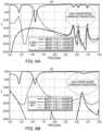
- Fig. 6A is a chart illustrating an illustrative antenna without perforation in accordance with an illustrative embodiment of the present invention.
- Fig. 6B is a chart illustrating an antenna with exemplary cavity perforations in accordance with an illustrative embodiment of the present invention.
- Both Figs. 6A and 6B illustrate the wideband sweep of the S parameters of an antenna with and without the cavities as described in accordance with illustrative embodiments of the present invention.
- those antennas with perforations i.e., those antennas with cavities in accordance with embodiments of the present invention
- Fig. 7A is a chart illustrating the high band gain of a RHCP antenna with and without perforation in accordance with an illustrative embodiment of the present invention. As can be observed from Fig. 7A , there is an improved gain when the antennas have the perforations (cavities) in accordance with an illustrative embodiment of the present invention.
- Fig. 7B is a chart illustrating the low band gain of a RHCP antenna with and without perforation in accordance with an illustrative embodiment of the present invention. As can be observed from Fig. 7B , there is an improved gain when the antennas have the perforations (cavities) in accordance with an illustrative embodiment of the present invention.
Landscapes
- Waveguide Aerials (AREA)
Applications Claiming Priority (2)
| Application Number | Priority Date | Filing Date | Title |
|---|---|---|---|
| US15/151,122 US10454174B2 (en) | 2016-05-10 | 2016-05-10 | Stacked patch antennas using dielectric substrates with patterned cavities |
| PCT/CA2017/050024 WO2017193206A1 (en) | 2016-05-10 | 2017-01-10 | Stacked patch antennas using dielectric substrates with patterned cavities |
Publications (3)
| Publication Number | Publication Date |
|---|---|
| EP3455905A1 EP3455905A1 (en) | 2019-03-20 |
| EP3455905A4 EP3455905A4 (en) | 2019-12-25 |
| EP3455905B1 true EP3455905B1 (en) | 2024-06-05 |
Family
ID=60266101
Family Applications (1)
| Application Number | Title | Priority Date | Filing Date |
|---|---|---|---|
| EP17795212.4A Active EP3455905B1 (en) | 2016-05-10 | 2017-01-10 | Stacked patch antennas using dielectric substrates with patterned cavities |
Country Status (8)
| Country | Link |
|---|---|
| US (3) | US10454174B2 (https=) |
| EP (1) | EP3455905B1 (https=) |
| JP (2) | JP2019515536A (https=) |
| KR (2) | KR20190002515A (https=) |
| CN (1) | CN109075437B (https=) |
| AU (1) | AU2017263727B2 (https=) |
| CA (1) | CA3017262C (https=) |
| WO (1) | WO2017193206A1 (https=) |
Families Citing this family (12)
| Publication number | Priority date | Publication date | Assignee | Title |
|---|---|---|---|---|
| US10461438B2 (en) * | 2016-03-17 | 2019-10-29 | Communication Components Antenna Inc. | Wideband multi-level antenna element and antenna array |
| US10454174B2 (en) | 2016-05-10 | 2019-10-22 | Novatel Inc. | Stacked patch antennas using dielectric substrates with patterned cavities |
| CN108198788A (zh) * | 2017-12-13 | 2018-06-22 | 深圳市时代速信科技有限公司 | 一种具有高射频信号垂直互联传输性能的ltcc基板 |
| US10978780B2 (en) * | 2018-01-24 | 2021-04-13 | Samsung Electro-Mechanics Co., Ltd. | Antenna apparatus and antenna module |
| CN109728401B (zh) * | 2018-12-26 | 2021-04-13 | 北京遥测技术研究所 | 一种高增益多频段导航天线 |
| US10700440B1 (en) * | 2019-01-25 | 2020-06-30 | Corning Incorporated | Antenna stack |
| JP2020127079A (ja) * | 2019-02-01 | 2020-08-20 | ソニーセミコンダクタソリューションズ株式会社 | アンテナ装置及び無線通信装置 |
| CN111755805B (zh) * | 2019-03-28 | 2022-02-18 | Oppo广东移动通信有限公司 | 天线模组和电子设备 |
| KR102211746B1 (ko) | 2019-08-30 | 2021-02-03 | 삼성전기주식회사 | 칩 안테나 |
| CN219513349U (zh) * | 2020-08-19 | 2023-08-11 | 株式会社村田制作所 | 通信装置 |
| KR20220163658A (ko) | 2021-06-03 | 2022-12-12 | 삼성전자주식회사 | 안테나를 포함하는 전자 장치 |
| CN116683175A (zh) * | 2023-07-05 | 2023-09-01 | 南通大学 | 一种双模条带型介质贴片的高增益滤波天线 |
Family Cites Families (53)
| Publication number | Priority date | Publication date | Assignee | Title |
|---|---|---|---|---|
| US3621154A (en) * | 1968-04-15 | 1971-11-16 | Shure Bros | Strain-sensitive semiconductive thin film electroacoustical transducer |
| US4089003A (en) * | 1977-02-07 | 1978-05-09 | Motorola, Inc. | Multifrequency microstrip antenna |
| US4316194A (en) * | 1980-11-24 | 1982-02-16 | The United States Of Americal As Represented By The Secretary Of The Army | Hemispherical coverage microstrip antenna |
| US5245745A (en) * | 1990-07-11 | 1993-09-21 | Ball Corporation | Method of making a thick-film patch antenna structure |
| US5444452A (en) * | 1992-07-13 | 1995-08-22 | Matsushita Electric Works, Ltd. | Dual frequency antenna |
| US5300936A (en) | 1992-09-30 | 1994-04-05 | Loral Aerospace Corp. | Multiple band antenna |
| US5386215A (en) | 1992-11-20 | 1995-01-31 | Massachusetts Institute Of Technology | Highly efficient planar antenna on a periodic dielectric structure |
| US5559055A (en) * | 1994-12-21 | 1996-09-24 | Advanced Micro Devices, Inc. | Method of decreased interlayer dielectric constant in a multilayer interconnect structure to increase device speed performance |
| JPH08298407A (ja) | 1995-04-26 | 1996-11-12 | Nec Eng Ltd | プリントアンテナ |
| JPH0998016A (ja) * | 1995-10-02 | 1997-04-08 | Mitsubishi Electric Corp | マイクロストリップアンテナ |
| JPH09130136A (ja) * | 1995-11-01 | 1997-05-16 | Toyo Commun Equip Co Ltd | 2周波共用マイクロストリップアンテナ |
| JP3471617B2 (ja) | 1997-09-30 | 2003-12-02 | 三菱電機株式会社 | 平面アンテナ装置 |
| US6118406A (en) * | 1998-12-21 | 2000-09-12 | The United States Of America As Represented By The Secretary Of The Navy | Broadband direct fed phased array antenna comprising stacked patches |
| US6307509B1 (en) | 1999-05-17 | 2001-10-23 | Trimble Navigation Limited | Patch antenna with custom dielectric |
| JP3554960B2 (ja) * | 1999-06-25 | 2004-08-18 | 株式会社村田製作所 | アンテナ装置およびそれを用いた通信装置 |
| US20020075186A1 (en) * | 2000-12-20 | 2002-06-20 | Hiroki Hamada | Chip antenna and method of manufacturing the same |
| JP2002217638A (ja) * | 2001-01-23 | 2002-08-02 | Mitsubishi Electric Corp | アンテナ装置 |
| US20040021606A1 (en) * | 2002-07-11 | 2004-02-05 | Alps Electric Co., Ltd. | Small plane antenna and composite antenna using the same |
| JP3825400B2 (ja) * | 2002-12-13 | 2006-09-27 | 京セラ株式会社 | アンテナ装置 |
| US6911941B2 (en) * | 2003-06-19 | 2005-06-28 | Harris Corporation | Dielectric substrate with selectively controlled effective permittivity and loss tangent |
| US7181834B2 (en) | 2003-10-27 | 2007-02-27 | Harris Corporation | Method of fabricating an RF substrate with selected electrical properties |
| DE102004035064A1 (de) * | 2004-07-20 | 2006-02-16 | Receptec Gmbh | Antennenmodul |
| US8111196B2 (en) * | 2006-09-15 | 2012-02-07 | Laird Technologies, Inc. | Stacked patch antennas |
| US20080297417A1 (en) | 2007-05-31 | 2008-12-04 | Symbol Technologies, Inc. | Light weight rugged microstrip element antenna incorporating skeleton dielectric spacer |
| US20090058731A1 (en) * | 2007-08-30 | 2009-03-05 | Gm Global Technology Operations, Inc. | Dual Band Stacked Patch Antenna |
| CN101299486A (zh) * | 2008-06-18 | 2008-11-05 | 北京邮电大学 | 一种覆盖高频和超高频及微波频段的rfid读写器天线 |
| DE102008043352A1 (de) * | 2008-10-31 | 2010-05-06 | Micro Systems Engineering Gmbh | Keramisches Substratmaterial, Verfahren zur Herstellung und Verwendung desselben sowie Antenne oder Antennenarray |
| CN101420066B (zh) * | 2008-11-21 | 2013-04-17 | 中国电子科技集团公司第三十八研究所 | 一种宽带单层微带贴片天线 |
| KR101113443B1 (ko) * | 2009-09-11 | 2012-02-29 | 삼성전기주식회사 | 패치 안테나 및 무선통신 모듈 |
| DE102010006809A1 (de) * | 2010-02-04 | 2011-08-04 | EADS Deutschland GmbH, 85521 | Gestapelte Mikrostreifen-Antenne |
| CN101931122B (zh) * | 2010-08-27 | 2013-04-03 | 电子科技大学 | 一种c/x双频段微带天线 |
| CN102176545B (zh) * | 2011-01-12 | 2015-06-17 | 电子科技大学 | 一种分层数目最少的电大尺寸高效龙伯透镜天线 |
| CN102255140A (zh) * | 2011-04-20 | 2011-11-23 | 东南大学 | 一种波束可控的透镜及维瓦尔第天线 |
| CN102480012B (zh) | 2011-04-28 | 2013-02-13 | 深圳光启高等理工研究院 | 一种超材料介质基板及其加工方法 |
| CN102760955B (zh) * | 2011-04-29 | 2015-02-04 | 深圳光启高等理工研究院 | 一种发散电磁波的超材料 |
| CN102760954B (zh) * | 2011-04-29 | 2014-12-24 | 深圳光启高等理工研究院 | 一种偏折电磁波的超材料 |
| CN102790288B (zh) * | 2011-05-18 | 2015-03-11 | 深圳光启创新技术有限公司 | 定向天线 |
| US9647328B2 (en) * | 2011-11-04 | 2017-05-09 | Kathrein-Werke Kg | Patch radiator |
| US9153863B2 (en) * | 2012-01-24 | 2015-10-06 | E I Du Pont De Nemours And Company | Low temperature co-fired ceramic (LTCC) system in a package (SiP) configurations for microwave/millimeter wave packaging applications |
| CN103367863B (zh) * | 2012-04-09 | 2015-02-18 | 中国科学院上海微系统与信息技术研究所 | 一种集成宽频带天线及其制作方法 |
| CN102706955B (zh) | 2012-05-31 | 2015-04-22 | 东北大学 | 基于单轴漏磁数据的管道缺陷特征提取方法及装置 |
| CN103107424B (zh) * | 2013-02-22 | 2014-12-03 | 哈尔滨工业大学 | 一种梯度折射率超常媒质透镜的制造方法 |
| CN103457029A (zh) * | 2013-09-04 | 2013-12-18 | 北京合众思壮科技股份有限公司 | 双频天线 |
| CN203660051U (zh) * | 2013-12-16 | 2014-06-18 | 电子科技大学 | 一种高阻硅基底高频微带天线 |
| US9653808B2 (en) * | 2014-07-10 | 2017-05-16 | Amotech Co., Ltd. | Multilayer patch antenna |
| CN204011731U (zh) * | 2014-08-06 | 2014-12-10 | 成都信息工程学院 | 复合介质微带天线 |
| CN104577316A (zh) * | 2014-12-30 | 2015-04-29 | 中国科学院上海微系统与信息技术研究所 | 一种应用于毫米波微带天线的垂直耦合馈电结构 |
| CN204333257U (zh) * | 2014-12-31 | 2015-05-13 | 深圳市华信天线技术有限公司 | 全频段收发一体化天线 |
| CN104836019A (zh) * | 2015-05-13 | 2015-08-12 | 西安电子科技大学 | 三频段共口径有源导航天线 |
| CN205016667U (zh) * | 2015-08-20 | 2016-02-03 | 广东顺德中山大学卡内基梅隆大学国际联合研究院 | 一种双层贴片的双频圆盘微带天线 |
| CN105305045B (zh) * | 2015-10-15 | 2017-11-07 | 厦门大学 | T型/斜l型引流缝隙双频宽带双圆极化微带叠层天线 |
| CN105161842B (zh) * | 2015-10-15 | 2017-12-15 | 厦门大学 | 长袖衫型开口调谐环低仰角高增益北斗多频微带天线 |
| US10454174B2 (en) * | 2016-05-10 | 2019-10-22 | Novatel Inc. | Stacked patch antennas using dielectric substrates with patterned cavities |
-
2016
- 2016-05-10 US US15/151,122 patent/US10454174B2/en active Active
-
2017
- 2017-01-10 CA CA3017262A patent/CA3017262C/en active Active
- 2017-01-10 EP EP17795212.4A patent/EP3455905B1/en active Active
- 2017-01-10 KR KR1020187032292A patent/KR20190002515A/ko not_active Ceased
- 2017-01-10 JP JP2018554404A patent/JP2019515536A/ja active Pending
- 2017-01-10 WO PCT/CA2017/050024 patent/WO2017193206A1/en not_active Ceased
- 2017-01-10 KR KR1020237022517A patent/KR102631849B1/ko active Active
- 2017-01-10 CN CN201780023316.4A patent/CN109075437B/zh active Active
- 2017-01-10 AU AU2017263727A patent/AU2017263727B2/en active Active
-
2019
- 2019-09-10 US US16/566,096 patent/US10985467B2/en active Active
-
2021
- 2021-04-20 US US17/235,639 patent/US11888242B2/en active Active
- 2021-06-17 JP JP2021100694A patent/JP7230116B2/ja active Active
Also Published As
| Publication number | Publication date |
|---|---|
| CA3017262C (en) | 2023-09-12 |
| WO2017193206A1 (en) | 2017-11-16 |
| KR102631849B1 (ko) | 2024-02-01 |
| US20210257737A1 (en) | 2021-08-19 |
| JP7230116B2 (ja) | 2023-02-28 |
| EP3455905A4 (en) | 2019-12-25 |
| JP2021153330A (ja) | 2021-09-30 |
| US20170331192A1 (en) | 2017-11-16 |
| US11888242B2 (en) | 2024-01-30 |
| US10454174B2 (en) | 2019-10-22 |
| EP3455905A1 (en) | 2019-03-20 |
| CN109075437B (zh) | 2022-05-24 |
| KR20230107402A (ko) | 2023-07-14 |
| US20200006854A1 (en) | 2020-01-02 |
| KR20190002515A (ko) | 2019-01-08 |
| AU2017263727B2 (en) | 2021-09-02 |
| US10985467B2 (en) | 2021-04-20 |
| JP2019515536A (ja) | 2019-06-06 |
| CN109075437A (zh) | 2018-12-21 |
| AU2017263727A1 (en) | 2018-09-06 |
| CA3017262A1 (en) | 2017-11-16 |
Similar Documents
| Publication | Publication Date | Title |
|---|---|---|
| EP3455905B1 (en) | Stacked patch antennas using dielectric substrates with patterned cavities | |
| US7538728B1 (en) | Antenna and resonant frequency tuning method thereof | |
| CN1947304B (zh) | 带有高度弯曲槽的多频带紧凑型pifa天线 | |
| KR102425825B1 (ko) | 다중 공진 안테나 장치 | |
| US7619568B2 (en) | Patch antenna including septa for bandwidth control | |
| US7292204B1 (en) | Dielectric resonator antenna with a caved well | |
| US8035568B2 (en) | Electromagnetic reactive edge treatment | |
| US11962086B2 (en) | Slot antenna and electronic device comprising said slot antenna | |
| CN103247849A (zh) | 天线装置 | |
| TWI524589B (zh) | 低阻抗槽饋入天線 | |
| US20180123251A1 (en) | Periodically rippled antenna | |
| CN112803159A (zh) | 一种馈电线阵与雷达天线 | |
| Dal Chiele et al. | RF-MEMS-controlled Minkowski fractal antenna for dual-band applications | |
| KR20150011711A (ko) | 이중 급전방식의 광대역 패치안테나 및 그 제조방법 | |
| KR101055671B1 (ko) | Gps/glonass 수신용 패치 안테나 및 그의 어셈블리 | |
| SE528069C3 (sv) | Antennanordning | |
| SE521833C2 (sv) | Antennanordning innefattande en icke-galvaniskt kopplad matningsanordning | |
| JP4301290B2 (ja) | インピーダンス変換方法および共平面多層インピーダンス変換器 | |
| JP2023039343A (ja) | プリントダイポールアンテナおよびプリントダイポールアンテナの指向性主ビーム方向の調整方法 | |
| Aziz | DUAL BAND MSA DESIGNS FOR GPS AND GSM APPLICATIONS |
Legal Events
| Date | Code | Title | Description |
|---|---|---|---|
| STAA | Information on the status of an ep patent application or granted ep patent |
Free format text: STATUS: THE INTERNATIONAL PUBLICATION HAS BEEN MADE |
|
| PUAI | Public reference made under article 153(3) epc to a published international application that has entered the european phase |
Free format text: ORIGINAL CODE: 0009012 |
|
| STAA | Information on the status of an ep patent application or granted ep patent |
Free format text: STATUS: REQUEST FOR EXAMINATION WAS MADE |
|
| 17P | Request for examination filed |
Effective date: 20181004 |
|
| AK | Designated contracting states |
Kind code of ref document: A1 Designated state(s): AL AT BE BG CH CY CZ DE DK EE ES FI FR GB GR HR HU IE IS IT LI LT LU LV MC MK MT NL NO PL PT RO RS SE SI SK SM TR |
|
| AX | Request for extension of the european patent |
Extension state: BA ME |
|
| DAV | Request for validation of the european patent (deleted) | ||
| DAX | Request for extension of the european patent (deleted) | ||
| A4 | Supplementary search report drawn up and despatched |
Effective date: 20191125 |
|
| RIC1 | Information provided on ipc code assigned before grant |
Ipc: H05K 3/42 20060101ALI20191119BHEP Ipc: H01Q 1/38 20060101AFI20191119BHEP Ipc: H01Q 9/04 20060101ALI20191119BHEP Ipc: G01S 19/36 20100101ALI20191119BHEP Ipc: H05K 1/03 20060101ALI20191119BHEP |
|
| STAA | Information on the status of an ep patent application or granted ep patent |
Free format text: STATUS: EXAMINATION IS IN PROGRESS |
|
| 17Q | First examination report despatched |
Effective date: 20210706 |
|
| GRAP | Despatch of communication of intention to grant a patent |
Free format text: ORIGINAL CODE: EPIDOSNIGR1 |
|
| STAA | Information on the status of an ep patent application or granted ep patent |
Free format text: STATUS: GRANT OF PATENT IS INTENDED |
|
| INTG | Intention to grant announced |
Effective date: 20231127 |
|
| GRAJ | Information related to disapproval of communication of intention to grant by the applicant or resumption of examination proceedings by the epo deleted |
Free format text: ORIGINAL CODE: EPIDOSDIGR1 |
|
| STAA | Information on the status of an ep patent application or granted ep patent |
Free format text: STATUS: EXAMINATION IS IN PROGRESS |
|
| INTC | Intention to grant announced (deleted) | ||
| GRAP | Despatch of communication of intention to grant a patent |
Free format text: ORIGINAL CODE: EPIDOSNIGR1 |
|
| STAA | Information on the status of an ep patent application or granted ep patent |
Free format text: STATUS: GRANT OF PATENT IS INTENDED |
|
| GRAS | Grant fee paid |
Free format text: ORIGINAL CODE: EPIDOSNIGR3 |
|
| INTG | Intention to grant announced |
Effective date: 20240328 |
|
| GRAA | (expected) grant |
Free format text: ORIGINAL CODE: 0009210 |
|
| STAA | Information on the status of an ep patent application or granted ep patent |
Free format text: STATUS: THE PATENT HAS BEEN GRANTED |
|
| RAP3 | Party data changed (applicant data changed or rights of an application transferred) |
Owner name: NOVATEL, INC. |
|
| AK | Designated contracting states |
Kind code of ref document: B1 Designated state(s): AL AT BE BG CH CY CZ DE DK EE ES FI FR GB GR HR HU IE IS IT LI LT LU LV MC MK MT NL NO PL PT RO RS SE SI SK SM TR |
|
| REG | Reference to a national code |
Ref country code: GB Ref legal event code: FG4D |
|
| REG | Reference to a national code |
Ref country code: CH Ref legal event code: EP |
|
| REG | Reference to a national code |
Ref country code: DE Ref legal event code: R096 Ref document number: 602017082434 Country of ref document: DE |
|
| REG | Reference to a national code |
Ref country code: IE Ref legal event code: FG4D |
|
| REG | Reference to a national code |
Ref country code: LT Ref legal event code: MG9D |
|
| PG25 | Lapsed in a contracting state [announced via postgrant information from national office to epo] |
Ref country code: BG Free format text: LAPSE BECAUSE OF FAILURE TO SUBMIT A TRANSLATION OF THE DESCRIPTION OR TO PAY THE FEE WITHIN THE PRESCRIBED TIME-LIMIT Effective date: 20240605 |
|
| REG | Reference to a national code |
Ref country code: NL Ref legal event code: MP Effective date: 20240605 |
|
| PG25 | Lapsed in a contracting state [announced via postgrant information from national office to epo] |
Ref country code: FI Free format text: LAPSE BECAUSE OF FAILURE TO SUBMIT A TRANSLATION OF THE DESCRIPTION OR TO PAY THE FEE WITHIN THE PRESCRIBED TIME-LIMIT Effective date: 20240605 Ref country code: HR Free format text: LAPSE BECAUSE OF FAILURE TO SUBMIT A TRANSLATION OF THE DESCRIPTION OR TO PAY THE FEE WITHIN THE PRESCRIBED TIME-LIMIT Effective date: 20240605 |
|
| PG25 | Lapsed in a contracting state [announced via postgrant information from national office to epo] |
Ref country code: GR Free format text: LAPSE BECAUSE OF FAILURE TO SUBMIT A TRANSLATION OF THE DESCRIPTION OR TO PAY THE FEE WITHIN THE PRESCRIBED TIME-LIMIT Effective date: 20240906 |
|
| PG25 | Lapsed in a contracting state [announced via postgrant information from national office to epo] |
Ref country code: ES Free format text: LAPSE BECAUSE OF FAILURE TO SUBMIT A TRANSLATION OF THE DESCRIPTION OR TO PAY THE FEE WITHIN THE PRESCRIBED TIME-LIMIT Effective date: 20240605 |
|
| PG25 | Lapsed in a contracting state [announced via postgrant information from national office to epo] |
Ref country code: LV Free format text: LAPSE BECAUSE OF FAILURE TO SUBMIT A TRANSLATION OF THE DESCRIPTION OR TO PAY THE FEE WITHIN THE PRESCRIBED TIME-LIMIT Effective date: 20240605 |
|
| PG25 | Lapsed in a contracting state [announced via postgrant information from national office to epo] |
Ref country code: NO Free format text: LAPSE BECAUSE OF FAILURE TO SUBMIT A TRANSLATION OF THE DESCRIPTION OR TO PAY THE FEE WITHIN THE PRESCRIBED TIME-LIMIT Effective date: 20240905 Ref country code: LV Free format text: LAPSE BECAUSE OF FAILURE TO SUBMIT A TRANSLATION OF THE DESCRIPTION OR TO PAY THE FEE WITHIN THE PRESCRIBED TIME-LIMIT Effective date: 20240605 Ref country code: HR Free format text: LAPSE BECAUSE OF FAILURE TO SUBMIT A TRANSLATION OF THE DESCRIPTION OR TO PAY THE FEE WITHIN THE PRESCRIBED TIME-LIMIT Effective date: 20240605 Ref country code: GR Free format text: LAPSE BECAUSE OF FAILURE TO SUBMIT A TRANSLATION OF THE DESCRIPTION OR TO PAY THE FEE WITHIN THE PRESCRIBED TIME-LIMIT Effective date: 20240906 Ref country code: FI Free format text: LAPSE BECAUSE OF FAILURE TO SUBMIT A TRANSLATION OF THE DESCRIPTION OR TO PAY THE FEE WITHIN THE PRESCRIBED TIME-LIMIT Effective date: 20240605 Ref country code: ES Free format text: LAPSE BECAUSE OF FAILURE TO SUBMIT A TRANSLATION OF THE DESCRIPTION OR TO PAY THE FEE WITHIN THE PRESCRIBED TIME-LIMIT Effective date: 20240605 Ref country code: BG Free format text: LAPSE BECAUSE OF FAILURE TO SUBMIT A TRANSLATION OF THE DESCRIPTION OR TO PAY THE FEE WITHIN THE PRESCRIBED TIME-LIMIT Effective date: 20240605 Ref country code: RS Free format text: LAPSE BECAUSE OF FAILURE TO SUBMIT A TRANSLATION OF THE DESCRIPTION OR TO PAY THE FEE WITHIN THE PRESCRIBED TIME-LIMIT Effective date: 20240905 |
|
| PG25 | Lapsed in a contracting state [announced via postgrant information from national office to epo] |
Ref country code: NL Free format text: LAPSE BECAUSE OF FAILURE TO SUBMIT A TRANSLATION OF THE DESCRIPTION OR TO PAY THE FEE WITHIN THE PRESCRIBED TIME-LIMIT Effective date: 20240605 |
|
| REG | Reference to a national code |
Ref country code: AT Ref legal event code: MK05 Ref document number: 1693138 Country of ref document: AT Kind code of ref document: T Effective date: 20240605 |
|
| PG25 | Lapsed in a contracting state [announced via postgrant information from national office to epo] |
Ref country code: NL Free format text: LAPSE BECAUSE OF FAILURE TO SUBMIT A TRANSLATION OF THE DESCRIPTION OR TO PAY THE FEE WITHIN THE PRESCRIBED TIME-LIMIT Effective date: 20240605 |
|
| PG25 | Lapsed in a contracting state [announced via postgrant information from national office to epo] |
Ref country code: PT Free format text: LAPSE BECAUSE OF FAILURE TO SUBMIT A TRANSLATION OF THE DESCRIPTION OR TO PAY THE FEE WITHIN THE PRESCRIBED TIME-LIMIT Effective date: 20241007 |
|
| PG25 | Lapsed in a contracting state [announced via postgrant information from national office to epo] |
Ref country code: PT Free format text: LAPSE BECAUSE OF FAILURE TO SUBMIT A TRANSLATION OF THE DESCRIPTION OR TO PAY THE FEE WITHIN THE PRESCRIBED TIME-LIMIT Effective date: 20241007 |
|
| PG25 | Lapsed in a contracting state [announced via postgrant information from national office to epo] |
Ref country code: PL Free format text: LAPSE BECAUSE OF FAILURE TO SUBMIT A TRANSLATION OF THE DESCRIPTION OR TO PAY THE FEE WITHIN THE PRESCRIBED TIME-LIMIT Effective date: 20240605 |
|
| PG25 | Lapsed in a contracting state [announced via postgrant information from national office to epo] |
Ref country code: EE Free format text: LAPSE BECAUSE OF FAILURE TO SUBMIT A TRANSLATION OF THE DESCRIPTION OR TO PAY THE FEE WITHIN THE PRESCRIBED TIME-LIMIT Effective date: 20240605 |
|
| PG25 | Lapsed in a contracting state [announced via postgrant information from national office to epo] |
Ref country code: AT Free format text: LAPSE BECAUSE OF FAILURE TO SUBMIT A TRANSLATION OF THE DESCRIPTION OR TO PAY THE FEE WITHIN THE PRESCRIBED TIME-LIMIT Effective date: 20240605 Ref country code: IS Free format text: LAPSE BECAUSE OF FAILURE TO SUBMIT A TRANSLATION OF THE DESCRIPTION OR TO PAY THE FEE WITHIN THE PRESCRIBED TIME-LIMIT Effective date: 20241005 |
|
| PG25 | Lapsed in a contracting state [announced via postgrant information from national office to epo] |
Ref country code: CZ Free format text: LAPSE BECAUSE OF FAILURE TO SUBMIT A TRANSLATION OF THE DESCRIPTION OR TO PAY THE FEE WITHIN THE PRESCRIBED TIME-LIMIT Effective date: 20240605 |
|
| PG25 | Lapsed in a contracting state [announced via postgrant information from national office to epo] |
Ref country code: RO Free format text: LAPSE BECAUSE OF FAILURE TO SUBMIT A TRANSLATION OF THE DESCRIPTION OR TO PAY THE FEE WITHIN THE PRESCRIBED TIME-LIMIT Effective date: 20240605 Ref country code: SK Free format text: LAPSE BECAUSE OF FAILURE TO SUBMIT A TRANSLATION OF THE DESCRIPTION OR TO PAY THE FEE WITHIN THE PRESCRIBED TIME-LIMIT Effective date: 20240605 |
|
| PG25 | Lapsed in a contracting state [announced via postgrant information from national office to epo] |
Ref country code: SM Free format text: LAPSE BECAUSE OF FAILURE TO SUBMIT A TRANSLATION OF THE DESCRIPTION OR TO PAY THE FEE WITHIN THE PRESCRIBED TIME-LIMIT Effective date: 20240605 |
|
| PG25 | Lapsed in a contracting state [announced via postgrant information from national office to epo] |
Ref country code: SM Free format text: LAPSE BECAUSE OF FAILURE TO SUBMIT A TRANSLATION OF THE DESCRIPTION OR TO PAY THE FEE WITHIN THE PRESCRIBED TIME-LIMIT Effective date: 20240605 Ref country code: SK Free format text: LAPSE BECAUSE OF FAILURE TO SUBMIT A TRANSLATION OF THE DESCRIPTION OR TO PAY THE FEE WITHIN THE PRESCRIBED TIME-LIMIT Effective date: 20240605 Ref country code: RO Free format text: LAPSE BECAUSE OF FAILURE TO SUBMIT A TRANSLATION OF THE DESCRIPTION OR TO PAY THE FEE WITHIN THE PRESCRIBED TIME-LIMIT Effective date: 20240605 Ref country code: PL Free format text: LAPSE BECAUSE OF FAILURE TO SUBMIT A TRANSLATION OF THE DESCRIPTION OR TO PAY THE FEE WITHIN THE PRESCRIBED TIME-LIMIT Effective date: 20240605 Ref country code: IS Free format text: LAPSE BECAUSE OF FAILURE TO SUBMIT A TRANSLATION OF THE DESCRIPTION OR TO PAY THE FEE WITHIN THE PRESCRIBED TIME-LIMIT Effective date: 20241005 Ref country code: EE Free format text: LAPSE BECAUSE OF FAILURE TO SUBMIT A TRANSLATION OF THE DESCRIPTION OR TO PAY THE FEE WITHIN THE PRESCRIBED TIME-LIMIT Effective date: 20240605 Ref country code: CZ Free format text: LAPSE BECAUSE OF FAILURE TO SUBMIT A TRANSLATION OF THE DESCRIPTION OR TO PAY THE FEE WITHIN THE PRESCRIBED TIME-LIMIT Effective date: 20240605 Ref country code: AT Free format text: LAPSE BECAUSE OF FAILURE TO SUBMIT A TRANSLATION OF THE DESCRIPTION OR TO PAY THE FEE WITHIN THE PRESCRIBED TIME-LIMIT Effective date: 20240605 |
|
| PG25 | Lapsed in a contracting state [announced via postgrant information from national office to epo] |
Ref country code: IT Free format text: LAPSE BECAUSE OF FAILURE TO SUBMIT A TRANSLATION OF THE DESCRIPTION OR TO PAY THE FEE WITHIN THE PRESCRIBED TIME-LIMIT Effective date: 20240605 |
|
| REG | Reference to a national code |
Ref country code: DE Ref legal event code: R097 Ref document number: 602017082434 Country of ref document: DE |
|
| PLBE | No opposition filed within time limit |
Free format text: ORIGINAL CODE: 0009261 |
|
| STAA | Information on the status of an ep patent application or granted ep patent |
Free format text: STATUS: NO OPPOSITION FILED WITHIN TIME LIMIT |
|
| PG25 | Lapsed in a contracting state [announced via postgrant information from national office to epo] |
Ref country code: DK Free format text: LAPSE BECAUSE OF FAILURE TO SUBMIT A TRANSLATION OF THE DESCRIPTION OR TO PAY THE FEE WITHIN THE PRESCRIBED TIME-LIMIT Effective date: 20240605 |
|
| 26N | No opposition filed |
Effective date: 20250306 |
|
| PG25 | Lapsed in a contracting state [announced via postgrant information from national office to epo] |
Ref country code: SE Free format text: LAPSE BECAUSE OF FAILURE TO SUBMIT A TRANSLATION OF THE DESCRIPTION OR TO PAY THE FEE WITHIN THE PRESCRIBED TIME-LIMIT Effective date: 20240605 |
|
| PG25 | Lapsed in a contracting state [announced via postgrant information from national office to epo] |
Ref country code: MC Free format text: LAPSE BECAUSE OF FAILURE TO SUBMIT A TRANSLATION OF THE DESCRIPTION OR TO PAY THE FEE WITHIN THE PRESCRIBED TIME-LIMIT Effective date: 20240605 Ref country code: LU Free format text: LAPSE BECAUSE OF NON-PAYMENT OF DUE FEES Effective date: 20250110 |
|
| PG25 | Lapsed in a contracting state [announced via postgrant information from national office to epo] |
Ref country code: BE Free format text: LAPSE BECAUSE OF NON-PAYMENT OF DUE FEES Effective date: 20250131 |
|
| REG | Reference to a national code |
Ref country code: BE Ref legal event code: MM Effective date: 20250131 |
|
| PG25 | Lapsed in a contracting state [announced via postgrant information from national office to epo] |
Ref country code: IE Free format text: LAPSE BECAUSE OF NON-PAYMENT OF DUE FEES Effective date: 20250110 |
|
| REG | Reference to a national code |
Ref country code: CH Ref legal event code: U11 Free format text: ST27 STATUS EVENT CODE: U-0-0-U10-U11 (AS PROVIDED BY THE NATIONAL OFFICE) Effective date: 20260201 |
|
| PGFP | Annual fee paid to national office [announced via postgrant information from national office to epo] |
Ref country code: GB Payment date: 20260127 Year of fee payment: 10 |
|
| PGFP | Annual fee paid to national office [announced via postgrant information from national office to epo] |
Ref country code: DE Payment date: 20260128 Year of fee payment: 10 |
|
| PGFP | Annual fee paid to national office [announced via postgrant information from national office to epo] |
Ref country code: FR Payment date: 20260126 Year of fee payment: 10 |
|
| PGFP | Annual fee paid to national office [announced via postgrant information from national office to epo] |
Ref country code: CH Payment date: 20260201 Year of fee payment: 10 |