EP3453320A1 - Pressure pulse wave sensor, pulse wave detection device, and biological information measurement device - Google Patents
Pressure pulse wave sensor, pulse wave detection device, and biological information measurement device Download PDFInfo
- Publication number
- EP3453320A1 EP3453320A1 EP17789378.1A EP17789378A EP3453320A1 EP 3453320 A1 EP3453320 A1 EP 3453320A1 EP 17789378 A EP17789378 A EP 17789378A EP 3453320 A1 EP3453320 A1 EP 3453320A1
- Authority
- EP
- European Patent Office
- Prior art keywords
- pulse wave
- pressure pulse
- faces
- sensor
- wave sensor
- Prior art date
- Legal status (The legal status is an assumption and is not a legal conclusion. Google has not performed a legal analysis and makes no representation as to the accuracy of the status listed.)
- Granted
Links
Images





Classifications
-
- A—HUMAN NECESSITIES
- A61—MEDICAL OR VETERINARY SCIENCE; HYGIENE
- A61B—DIAGNOSIS; SURGERY; IDENTIFICATION
- A61B5/00—Measuring for diagnostic purposes; Identification of persons
- A61B5/02—Detecting, measuring or recording for evaluating the cardiovascular system, e.g. pulse, heart rate, blood pressure or blood flow
- A61B5/021—Measuring pressure in heart or blood vessels
- A61B5/022—Measuring pressure in heart or blood vessels by applying pressure to close blood vessels, e.g. against the skin; Ophthalmodynamometers
- A61B5/0225—Measuring pressure in heart or blood vessels by applying pressure to close blood vessels, e.g. against the skin; Ophthalmodynamometers the pressure being controlled by electric signals, e.g. derived from Korotkoff sounds
-
- A—HUMAN NECESSITIES
- A61—MEDICAL OR VETERINARY SCIENCE; HYGIENE
- A61B—DIAGNOSIS; SURGERY; IDENTIFICATION
- A61B5/00—Measuring for diagnostic purposes; Identification of persons
- A61B5/02—Detecting, measuring or recording for evaluating the cardiovascular system, e.g. pulse, heart rate, blood pressure or blood flow
-
- A—HUMAN NECESSITIES
- A61—MEDICAL OR VETERINARY SCIENCE; HYGIENE
- A61B—DIAGNOSIS; SURGERY; IDENTIFICATION
- A61B5/00—Measuring for diagnostic purposes; Identification of persons
- A61B5/02—Detecting, measuring or recording for evaluating the cardiovascular system, e.g. pulse, heart rate, blood pressure or blood flow
- A61B5/021—Measuring pressure in heart or blood vessels
- A61B5/02108—Measuring pressure in heart or blood vessels from analysis of pulse wave characteristics
-
- A—HUMAN NECESSITIES
- A61—MEDICAL OR VETERINARY SCIENCE; HYGIENE
- A61B—DIAGNOSIS; SURGERY; IDENTIFICATION
- A61B5/00—Measuring for diagnostic purposes; Identification of persons
- A61B5/68—Arrangements of detecting, measuring or recording means, e.g. sensors, in relation to patient
- A61B5/6801—Arrangements of detecting, measuring or recording means, e.g. sensors, in relation to patient specially adapted to be attached to or worn on the body surface
- A61B5/6843—Monitoring or controlling sensor contact pressure
-
- A—HUMAN NECESSITIES
- A61—MEDICAL OR VETERINARY SCIENCE; HYGIENE
- A61B—DIAGNOSIS; SURGERY; IDENTIFICATION
- A61B2562/00—Details of sensors; Constructional details of sensor housings or probes; Accessories for sensors
- A61B2562/02—Details of sensors specially adapted for in-vivo measurements
- A61B2562/0247—Pressure sensors
-
- A—HUMAN NECESSITIES
- A61—MEDICAL OR VETERINARY SCIENCE; HYGIENE
- A61B—DIAGNOSIS; SURGERY; IDENTIFICATION
- A61B2562/00—Details of sensors; Constructional details of sensor housings or probes; Accessories for sensors
- A61B2562/04—Arrangements of multiple sensors of the same type
- A61B2562/043—Arrangements of multiple sensors of the same type in a linear array
-
- A—HUMAN NECESSITIES
- A61—MEDICAL OR VETERINARY SCIENCE; HYGIENE
- A61B—DIAGNOSIS; SURGERY; IDENTIFICATION
- A61B2562/00—Details of sensors; Constructional details of sensor housings or probes; Accessories for sensors
- A61B2562/16—Details of sensor housings or probes; Details of structural supports for sensors
-
- A—HUMAN NECESSITIES
- A61—MEDICAL OR VETERINARY SCIENCE; HYGIENE
- A61B—DIAGNOSIS; SURGERY; IDENTIFICATION
- A61B2562/00—Details of sensors; Constructional details of sensor housings or probes; Accessories for sensors
- A61B2562/22—Arrangements of medical sensors with cables or leads; Connectors or couplings specifically adapted for medical sensors
- A61B2562/225—Connectors or couplings
- A61B2562/227—Sensors with electrical connectors
-
- A—HUMAN NECESSITIES
- A61—MEDICAL OR VETERINARY SCIENCE; HYGIENE
- A61B—DIAGNOSIS; SURGERY; IDENTIFICATION
- A61B5/00—Measuring for diagnostic purposes; Identification of persons
- A61B5/68—Arrangements of detecting, measuring or recording means, e.g. sensors, in relation to patient
- A61B5/6801—Arrangements of detecting, measuring or recording means, e.g. sensors, in relation to patient specially adapted to be attached to or worn on the body surface
- A61B5/6813—Specially adapted to be attached to a specific body part
- A61B5/6824—Arm or wrist
Definitions
- the present invention relates to a pressure pulse wave sensor, a pulse wave detector, and a biological information measurement device.
- a biological information measurement device is known that, in a state where a pressure sensor is directly made contact with a living body portion through which an artery such as the radial artery in the wrist passes, can measure biological information such as pulse or blood pressure by using information detected by this pressure sensor (see Patent Literature 1).
- the pressure sensor mounted on the biological information measurement device described in Patent Literature 1 is equipped with a circuit board, a spacer provided on this circuit board, a sensor chip provided on this spacer, a case for accommodating the circuit board, and a protection plate for protecting the circuit board.
- This protection plate is provided with an opening, and the sensor chip protrudes from this opening.
- Patent Literature 1 JP-A-4-67839
- the sensor chip protrudes from the opening of the protection plate.
- the surface of the sensor chip in the pressure sensor dominantly makes contact with the wrist, whereby the force applied to the surface of the sensor chip becomes large. Consequently, in the case that it is assumed that the biological information measurement device is attached for a long time such as a whole day, improving the durability of the sensor chip becomes a problem to be solved.
- the present invention has been made in consideration of the above-mentioned circumstances, and an object of the present invention is to provide a pressure pulse wave sensor capable of ensuring sufficient durability in the case of wearing the sensor for a long time and capable of suppressing manufacturing cost, a pulse wave detector, and a biological information measurement device.
- the pressure pulse wave sensor according to the present invention is equipped with sensor chips having pressure detection elements; a substrate to which the sensor chips are fixed; and a protection member for protecting the substrate and the sensor chips, wherein, in the vertical direction perpendicular to the detection faces of the sensor chips on which the pressure detection elements are formed, the protection member has opening sections disposed at positions opposed to the detection faces on the side opposite to the side of the fixture portion of the sensor chips and the substrate rather than the side of the pressure detection elements, and the space between the opening sections and the detection faces is filled with a filling material.
- the pulse wave detector according to the present invention is equipped with the pressure pulse wave sensor, the sensor chip of the pressure pulse wave sensor has an element row including the plurality of pressure detection elements arranged in one direction, and the outer peripheral face of the protection member is a face continuing to both the edges in the one direction of the top face in which the opening sections are formed and has inclined faces inclined with respect to the opening faces of the opening sections; the pulse wave detector is further equipped with a rotation mechanism for rotating the pressure pulse wave sensor around the respective directions orthogonal to the one direction and the vertical direction, and the inclination angle of the inclined faces is set to a value less than the maximum value of the rotation angle of the pressure pulse wave sensor capable of being rotated by the rotation mechanism.
- the biological information measurement device is equipped with the pulse wave detector and a biological information calculation section for calculating biological information on the basis of the pressure pulse wave detected by the pressure pulse wave sensor.
- the biological information measurement device is equipped with the pressure pulse wave sensor and the biological information calculation section for calculating biological information on the basis of the pressure pulse wave detected by the pressure pulse wave sensor.
- the present invention can provide a pressure pulse wave sensor capable of ensuring sufficient durability in the case of wearing the sensor for a long time and capable of suppressing manufacturing cost and a biological information measurement device equipped with this sensor.
- Fig. 1 is a schematic view showing the outline configuration of a biological information measurement device 100 according to an embodiment of the present invention.
- the biological information measurement device 100 is equipped with a housing 80, an air bag 70 supported by the housing 80, a rotation driving section 60 fixed to the air bag 70, and a pressure pulse wave sensor 10 rotatably supported by the rotation driving section 60.
- the biological information measurement device 100 is attached by a band, not shown, to a wrist of a person to be measured.
- the air bag 70 constitutes a pressing member for pressing the rotation driving section 60 and the pressure pulse wave sensor 10 against the body surface of the wrist.
- the internal pressure of the air bag 70 is adjusted by a pump, not shown, built in the housing 80.
- the pump is controlled by a control section that is built in the housing 80.
- the rotation driving section 60 has a rotation mechanism 61 for rotating the pressure pulse wave sensor 10 around the axes respectively extending in two directions orthogonal to each other along the detection face, described later, of the pressure pulse wave sensor 10 and an actuator 62 for driving the rotation mechanism 61.
- the actuator 62 is controlled by the control section built in the housing 80.
- the pressure pulse wave sensor 10 is a sensor for detecting a pressure pulse wave serving as a pressure oscillating wave and transmitted from the radial artery T passing through the inside of the wrist to the body surface in the state in which the pressure pulse wave sensor 10 is pressed by the air bag 70 against the body surface with a predetermined pressing force.
- the housing 80 incorporates a biological information calculation section, not shown, for calculating biological information, such as pulse rate, heart rate or blood pressure value, on the basis of the pressure pulse wave detected by the pressure pulse wave sensor 10.
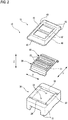
- Fig. 2 is an exploded perspective view showing the external configuration of the pressure pulse wave sensor 10 shown in Fig. 1 .
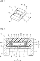
- Fig. 3 is a perspective view showing the outline configuration of the pressure pulse wave sensor 10 shown in Fig. 1 .
- the pressure pulse wave sensor 10 is equipped with two sensor sections 20 having a longitudinal shape along the X-direction, one of two directions, a flexible substrate 21 to which the two sensor sections 20 are fixed in the Y-d orthogonal to the X-direction, a base 30 to which the flexible substrate 21 is fixed, and a protection cover 40 that is fixed to the base 30 to which the flexible substrate 21 is fixed so as to serve as a protection member for protecting the two sensor sections 20.
- the base 30 has a rectangular planar shape as viewed in the Z-direction orthogonal to the X-direction and Y-direction and has a mounting face 32 on which the flexible substrate 21 is mounted.
- Two base through-holes 33 passing through the mounting face 32 in the Z-direction are provided in the mounting face 32; the number thereof corresponds to the number of the sensor sections 20.
- openings 34 having a size allowing the flexible substrate 21 to be inserted are provided at both the end positions in the Y-direction of the mounting face 32. Both the ends of the flexible substrate 21 are pulled out to the rear side of the base 30 through these openings 34.
- the planar shape of the protection cover 40 as viewed in the Z-direction is a rectangular shape similar to the external shape of the base 30 and has a size similar to the external shape thereof, and in the state in which the flexible substrate 21 is fixed to the base 30, the protection cover 40 is fixed to the peripheral face of the mounting face 32 of the base 30.
- the protection cover 40 In the state of being fixed to the base 30, the protection cover 40 has two opening sections 42 formed respectively at positions opposed to the two sensor sections 20.
- the outer peripheral face (the face exposed to the outside in the state shown in Fig. 3 ) of the protection cover 40 has a flat top face 41, inclined faces 44 continuing to the edges 45 of the top face 41, and vertical faces 46 continuing to the edges of the inclined faces 44 and perpendicular to the top face 41.
- the detailed shape of the protection cover 40 will be described later.
- Fig. 4 is a schematic view showing the external configuration of the sensor section 20 shown in Fig. 2 .
- Fig. 5 is a sectional schematic view taken on line V-V in Fig. 3 .
- the sensor section 20 is equipped with a sensor chip 22 and a container-like substrate 50 having a concave section 51, wherein the sensor chip 22 is fixed to the bottom face 52 of the concave section 51.
- the sensor chip 22 has a semiconductor substrate 23 made of a single crystal of silicon or a single crystal of a compound semiconductor, such as gallium arsenide.
- the semiconductor substrate 23 is formed into a rectangular shape so that the longitudinal direction thereof is oriented in the X-direction.
- An element row 25 including a plurality of pressure detection elements 24 arranged along the X-direction is formed on the surface of the semiconductor substrate 23.
- the pressure detection element 24 is an element for detecting the strain applied to the element as a pressure signal, and for example, a strain gauge resistance type element, a semiconductor piezo resistance type element or an electrostatic capacitance type element is used.
- the surface of the semiconductor substrate 23 is a flat face and this flat face constitutes a detection face 26 for detecting pressure.
- the direction perpendicular to the detection face 26 is the Z-direction.
- a chip-side terminal section 27 including electrode pads electrically connected to the respective pressure detection elements 24 is formed at each of both the end sections in the X-direction of the surface of the semiconductor substrate 23 (see Fig. 4 ).
- the substrate 50 is formed of a hard substrate, such as a ceramic substrate or a glass substrate, having rigidity sufficiently higher than that of the semiconductor substrate 23.
- the substrate 50 is formed into a rectangular shape so that the longitudinal direction thereof is oriented in the X-direction.
- a concave section recessed in the Z-direction perpendicular to the detection face 26 is formed in the face of the semiconductor substrate 23 opposite to the detection face 26 in the face of the semiconductor substrate 23 opposite to the detection face 26 .
- the semiconductor substrate 23 is configured so as to have a thin section (diaphragm), the thickness of which is smaller than that of the other portion in the Z-direction.
- the portion of the face of the semiconductor substrate 23 opposite to the detection face 26 excluding the concave section is fixed to the bottom face 52 of the concave section 51 of the substrate 50 with an adhesive 29.
- an ultraviolet curing resin is used for example.
- the semiconductor substrate 23 is fixed to the bottom face 52 of the concave section 51 so that the concave section of the semiconductor substrate 23 communicates with the atmosphere only through the through holes 54 formed in the bottom face of the concave section 51 of the substrate 50.
- through holes 211 are formed at the positions opposed to the through holes 54 of the substrate 50. These through holes 211 communicate with the base through holes 33 of the base 30. Hence, the inside of the concave section of the semiconductor substrate 23 is kept at the atmospheric pressure by the base through holes 33, the through holes 211, and the through holes 54.
- a substrate-side terminal section 53 including electrode pads for electrical connection to the respective electrode pads of the chip-side terminal section 27 is provided on the face of the substrate 50 in which the concave section 51 is formed.
- the electrode pads of the chip-side terminal section 27 and the electrode pads of the substrate-side terminal section 53 are connected via conductive members 28 made of gold, aluminum or the like.
- the conductive members 28 are covered therearound and protected with protection members 281 made of an insulation material, such as resin.
- protection members 281 made of an insulation material, such as resin.
- the space between the side face of the concave section 51 of the substrate 50 and both the semiconductor substrate 23 and the adhesive 29 is filled with a material 282 that is less changed in volume than the protection member 281 depending on temperature and humidity.
- the top face 41 of the protection cover 40 is disposed on the side opposite to the side of the fixture portion (the place where the adhesive 29 is located) of the sensor chips 22 and the substrate 50 rather than the side of the pressure detection elements 24, and the top face 41 is parallel with the detection face 26.
- the state in which the two faces are parallel with each other is the state in which the angle formed by the two faces is within the range of a tolerance with 0° taken as its center.
- the state in which the two faces are perpendicular with each other is the state in which the angle formed by the two faces is within the range of a tolerance with 90° taken as its center.
- the opening sections 42 each passing through the position opposed to the detection face 26 of each sensor chip 22 to the detection face 26 are formed in the top face 41 of the protection cover 40.
- the element row 25 entirely overlaps with the opening section 42 in a plan view in the Z-direction.
- the base 30, the sensor sections 20 and the flexible substrate 21 is filled with a filling material 55 as shown in Fig. 5 .
- the filling material 55 is also used to fill the opening sections 42 of the protection cover 40, and the surface 551 of the filling material 55 exposed to the outside is formed so as to be flush with the top face 41 of the protection cover 40.
- the surface 551 constitutes the opening faces of the opening sections 42.
- the flat face formed by the surface 551 of the filling material 55 and the top face 41 of the protection cover 40 is parallel with the detection faces 26 and forms a contact face making contact with the body surface of the person to be measured.
- a material having hardness lower than that of the protection cover 40 should be used for the filling material 55.
- ceramic is preferably used as the material of the protection cover 40, and an epoxy resin, a silicon resin or the like having hardness lower than that of ceramic is used as the filling material 55.
- the inclined faces 44 of the protection cover 40 continue to both the edges 45x in the X-direction of the top face 41 and are inclined faces inclined at an inclination angle ⁇ with respect to the face 551 so as to approach the sensor chips 22 in the Z-direction.
- the vertical faces 46 of the protection cover 40 are faces continuing to the inclined faces 44 and perpendicular to the surface 551.
- the vertical faces 46 are located on the side of the sensor chips 22 rather than the side of the surface 551 in the Z-direction and located outside the edges 45 of the top face 41 in a plan view as viewed in the Z-direction.
- the shape of the protection cover 40 in the cross section along the straight line extending in the Y-direction of the pressure pulse wave sensor 10 shown in Fig. 3 and passing through the top face 41 is similar to the shape of the protection cover 40 shown in Fig. 5 .
- the outer peripheral face of the protection cover 40 is a face continuing to both the edges in the Y-direction of the top face 41, and has the inclined faces 44 inclined with respect to the top face 41 so as to approach the sensor chips 22 and the vertical faces 46 continuing to the inclined faces 44.
- the respective side faces 31 of both the end sections of the base 30 in the X-direction and the Y-direction are formed so as to continue to the vertical faces 46 of the protection cover 40 without level difference in the state in which the protection cover 40 is fixed, and the vertical faces 46 and the side faces 31 are formed into the same face being parallel with the Z-direction.
- Fig. 6 is a plan view showing the pressure pulse wave sensor 10 shown in Fig. 3 , as viewed in the Z-direction. In Fig. 6 , only the positions of the conductive members 28 of the sensor sections 20 are shown, and the other components are omitted.
- the conductive members 28 of the sensor sections 20 are disposed at positions that do not overlap with the edges 45 of the top face 41 in a plan view as viewed in the Z-direction.
- the edges 45 of the top face 41 are portions to which the largest stress is applied in the state in which the top face 41 is pressed against the body surface.
- the conductive members 28 are formed of, for example, wire bonding, if a large force is applied thereto, wire breakage may occur.
- the conductive members 28 are located at positions that do not overlap with the edges 45 of the top face 41, the conductive members 28 are not located at positions below the portions to which the large stress is applied. Hence, even in the case that the pressure pulse wave sensor 10 is pressed against the body surface, the force to be applied to the conductive members 28 can be decreased, whereby wire breakage can be prevented.
- the rotation mechanism 61 of the biological information measurement device 100 shown in Fig. 1 is a mechanism for rotating the pressure pulse wave sensor 10 around the respective two axes extending in the X-direction and the Y-direction.
- the biological information measurement device 100 configured as described above is attached to a wrist so that the X-direction intersects the radial artery T (see Fig. 1 ) of the wrist from which a pressure pulse wave is detected.
- the control section increases the internal pressure of the air bag 70, thereby pressing the pressure pulse wave sensor 10 against the surface of the wrist.
- the control section determines the rotation angles around the respective two axes extending in the X-direction and the Y-direction of the pressure pulse wave sensor 10 so that the detection accuracy of a pressure pulse wave becomes maximum.
- the control section rotates the pressure pulse wave sensor 10 by the rotation angles determined as described above, detects a pressure pulse wave using the pressure detection elements 24 of the pressure pulse wave sensor 10 in the state in which the pressure pulse wave sensor 10 is pressed against the body surface with a predetermined pressing force, calculates biological information on the basis of the detected pressure pulse wave, and stores the biological information.
- the opening sections 42 of the protection cover 40 are provided above the detection faces 26 of the sensor chips 22, and the opening sections 42 are filled with the filling material 55, whereby the contact face making contact with the body surface is formed by the top face 41 of the protection cover 40 and the surface 551 of the filling material 55.
- the durability of the sensor chips 22 of the pressure pulse wave sensor 10 can be improved.
- the biological information measurement device 100 can be used for a long time while being attached to the wrist.
- the durability can be further improved by using a material having hardness higher than that of the filling material 55 as the material of the protection cover 40.
- the surface 551 of the filling material 55 can be made flat easily by using the flatness of the top face 41. Hence, the manufacturing cost thereof can be reduced. In the case that a material having hardness higher than that of the filling material 55 is used as the material of the protection cover 40, the surface 551 of the filling material 55 can be made flat more easily.
- the pressure pulse wave sensor 10 has a configuration in which the protection cover 40 has the inclined faces 44 continuing to both the edges 45x in the X-direction of the top face 41.
- the pressure pulse wave sensor 10 is rotated around the axis extending in the Y-direction (around the wrist) by the rotation driving section 60, the area of the protection cover 40 making contact with the body surface can be reduced.
- the biological information measurement device 100 is attached to the wrist so that the top face 41 of the protection cover 40 is located above the radial artery T; however, hard tissues, such as a radius and a tendon, exist around the radial artery T.
- the pressure pulse wave sensor 10 is rotated around the wrist, since the inclined faces 44 of the protection cover 40 can release the pressure from these hard tissues, the feeling of wearing the biological information measurement device 100 can be improved. Furthermore, since the rotation operation of the pressure pulse wave sensor 10 is hardly hindered by the hard tissues, the desired rotation angle can be maintained by small driving power and pressing force.
- the inclined faces 44 of the protection cover 40 may be curved faces instead of the flat faces.
- the protection cover 40 may be configured so as to have curved faces connecting the top face 41 to the vertical faces 46.
- the curved faces constitute faces continuing to both the edges in the X-direction of the top face 41 and intersecting the surface 551 and the respective faces perpendicular to the surfaces 551.
- the inclination angle ⁇ of the inclined face 44 shown in Fig. 5 is preferably set to a value less than the maximum value of the rotation angle (the rotation angle at the time when the state in which the detection face 26 is perpendicular to the direction of pressing the pressure pulse wave sensor 10 by the air bag 70 is used as a reference) by which the pressure pulse wave sensor 10 can be rotated around the axis extending in the Y-direction by the rotation mechanism 61.
- the pressure pulse wave sensor 10 is configured so that the protection cover 40 has the vertical faces 46.
- the sensor chip 22 requires to perform a work of acquiring the signals from the pressure detection elements 24 by applying pressure to the contact face in the state in which the contact face constituting the top face 41 and the surface 551 is accommodated in a sealed container in a manufacturing process.
- the vertical faces 46 are provided on the side of the base 30 rather than the side of the surface 551, in the case that a cap-shaped device is installed around the vertical faces 46, the interior of the device can be made hermetically sealed easily. Hence, the work for generating the calibration data can be made easy and the manufacturing cost can be reduced.
- Fig. 7 is a perspective view showing the external configuration of a protection cover 401, a modification of the protection cover 40 of the pressure pulse wave sensor 10 shown in Fig. 2 .
- the protection cover 401 is configured such that both the end faces in the Y-direction of the protection cover 40 are changed to the vertical faces 46 perpendicular to the surface 551.
- the vertical faces 46 are faces continuing to the edges in the Y-direction of the top face 41.
- the protection cover 40 since the edges in the Y-direction of the top face 41 are located away from the sensor chips 22, the stresses applied to the sensor chips 22 can be reduced, whereby the detection accuracy of the pressure pulse wave can be improved, and the durability of the pressure pulse wave sensor 10 can be improved.
- the outer peripheral face of the protection cover 40 of the pressure pulse wave sensor 10 may include only the top face 41 and the vertical faces 46 continuing to the edges 45 of the top face 41 and perpendicular to the surface 551. In other words, the inclined faces 44 on the outer peripheral face of the protection cover 40 are not essential.
- Fig. 8 is a sectional schematic view showing a pressure pulse wave sensor 12, a modification of the pressure pulse wave sensor 10 shown in Fig. 2 .
- the configuration of the pressure pulse wave sensor 12 shown in Fig. 8 is different from the configuration shown in Fig. 5 in that the outer peripheral face of the protection cover 40 includes the top face 41 and the vertical faces 46 continuing to the edges of the top face 41 and that the outer peripheral face of the protection cover 40 does not have the inclined faces 44.
- the pressure pulse wave sensor 12 is similar to the pressure pulse wave sensor 10 and a working effect similar thereto can be obtained.
- the edges of the top face 41 overlap with the vertical faces 46 in a plan view as viewed in the Z-direction.
- the configuration of the sensor section 20 to be mounted on the pressure pulse wave sensor 10 and the pressure pulse wave sensor 12 is not limited to those shown in Figs. 1 and 8 .
- the sensor section 20 may be changed to the sensor section 201 shown in Fig. 9 .
- the configuration of the sensor section 201 is the same as that of the sensor section 20 except that the substrate 50 is modified to a substrate 501 having a flat plate shape. Even in the case that the sensor section 201 configured as described above is used, the above-mentioned effects can be obtained.
- the pressure pulse wave sensor 10 is assumed to have two sensor sections 20, the pressure pulse wave sensor 10 may have only one sensor section 20.
- the rotation mechanism 61 is changed to a mechanism for rotating the pressure pulse wave sensor 10 only around the axis extending in the Y-direction.
- only one pressure detection element 24 may be formed on the surface of the sensor chip 22 of the sensor section 20.
- the rotation driving section 60 can be omitted.
- the pressure pulse wave sensor 10 may be configured so as to have three or more sensor sections 20 arranged in the Y-direction.
- top face 41 of the protection cover 40 is formed into a flat face that is parallel with the detection faces 26, the top face 41 of the protection cover 40 may be inclined with respect to the detection faces 26 as shown in Fig. 10 .
- the opening sections 42 formed in the top face 41 are filled with the filling material 55, and the opening faces of the opening section 42 are parallel with the detection faces 26. Even with the configuration described above, the durability can be improved.
- the biological information measurement device 100 to be attached to a wrist and used has been described above, the present invention can be applied to a type of biological information measurement device that is attached to a living body portion where an artery passes.
- the disclosed pressure pulse wave sensor is equipped with sensor chips having pressure detection elements; a substrate to which the sensor chips are fixed; and a protection member for protecting the substrate and the sensor chips, wherein, in the vertical direction perpendicular to the detection faces of the sensor chips on which the pressure detection elements are formed, the protection member has opening sections disposed at positions opposed to the detection faces on the side opposite to the side of the fixture portion of the sensor chips and the substrate rather than the side of the pressure detection elements, and the space between the opening sections and the detection faces is filled with a filling material.
- the protection member is made of a material having hardness higher than that of the filling material.
- the protection member is made of ceramic.
- the outer peripheral face of the protection member has vertical faces perpendicular to the opening faces of the opening sections, and the vertical faces are located on the side of the sensor chips rather than the side of the opening face in the vertical direction and overlap with the edges of the top face of the protection member in which the opening sections are formed or located outside the edges of the top face in a plan view as viewed in the vertical direction.
- the sensor chip has an element row including the plurality of pressure detection elements arranged in one direction, and the outer peripheral face of the protection member is a face continuing to both the edges in the one direction of the top face in which the opening sections are formed and has faces intersecting the opening faces of the opening sections and the respective faces perpendicular to the opening faces.
- the disclosed pressure pulse wave sensor is further equipped with substrate-side terminal sections provided on the substrate and used for electrical connection to the terminal sections provided at the ends in the one direction of the sensor chips and conductive members for connecting the terminal sections of the sensor chips and the substrate-side terminal sections, wherein the conductive members are disposed at positions that do not overlap with the edges of the top face in a plan view as viewed in the vertical direction.
- the outer peripheral face of the protection member is a face continuing to both the edges in the respective directions orthogonal to the one direction and the vertical direction of the top face and has vertical faces perpendicular to the opening faces of the opening sections.
- the disclosed pulse wave detector is equipped with the pressure pulse wave sensor and a rotation mechanism for rotating the pressure pulse wave sensor around the directions respectively orthogonal to the one direction and the vertical direction, wherein the continuing face has inclined faces inclined with respect to the opening faces, the inclination angle of the inclined faces is set to a value less than the maximum value of the rotation angle of the pressure pulse wave sensor capable of being rotated by the rotation mechanism.
- the disclosed biological information measurement device is equipped with the pulse wave detector and a biological information calculation section for calculating biological information on the basis of the pressure pulse wave detected by the pressure pulse wave sensor.
- the disclosed biological information measurement device is equipped with the pressure pulse wave sensor and the biological information calculation section for calculating biological information on the basis of the pressure pulse wave detected by the pressure pulse wave sensor.
- the present invention is highly convenient and effective when applied particularly to a wrist-attached sphygmomanometer and the like.
Landscapes
- Health & Medical Sciences (AREA)
- Life Sciences & Earth Sciences (AREA)
- Cardiology (AREA)
- Heart & Thoracic Surgery (AREA)
- Molecular Biology (AREA)
- Veterinary Medicine (AREA)
- Biophysics (AREA)
- Pathology (AREA)
- Engineering & Computer Science (AREA)
- Biomedical Technology (AREA)
- Public Health (AREA)
- Medical Informatics (AREA)
- Physics & Mathematics (AREA)
- Surgery (AREA)
- Animal Behavior & Ethology (AREA)
- General Health & Medical Sciences (AREA)
- Vascular Medicine (AREA)
- Physiology (AREA)
- Ophthalmology & Optometry (AREA)
- Measuring Pulse, Heart Rate, Blood Pressure Or Blood Flow (AREA)
Abstract
Description
- The present invention relates to a pressure pulse wave sensor, a pulse wave detector, and a biological information measurement device.
- A biological information measurement device is known that, in a state where a pressure sensor is directly made contact with a living body portion through which an artery such as the radial artery in the wrist passes, can measure biological information such as pulse or blood pressure by using information detected by this pressure sensor (see Patent Literature 1).
- The pressure sensor mounted on the biological information measurement device described in Patent Literature 1 is equipped with a circuit board, a spacer provided on this circuit board, a sensor chip provided on this spacer, a case for accommodating the circuit board, and a protection plate for protecting the circuit board. This protection plate is provided with an opening, and the sensor chip protrudes from this opening.
- Patent Literature 1:
JP-A-4-67839 - In the sensor section described in Patent Literature 1, the sensor chip protrudes from the opening of the protection plate. Hence, the surface of the sensor chip in the pressure sensor dominantly makes contact with the wrist, whereby the force applied to the surface of the sensor chip becomes large. Consequently, in the case that it is assumed that the biological information measurement device is attached for a long time such as a whole day, improving the durability of the sensor chip becomes a problem to be solved.
- The present invention has been made in consideration of the above-mentioned circumstances, and an object of the present invention is to provide a pressure pulse wave sensor capable of ensuring sufficient durability in the case of wearing the sensor for a long time and capable of suppressing manufacturing cost, a pulse wave detector, and a biological information measurement device.
- The pressure pulse wave sensor according to the present invention is equipped with sensor chips having pressure detection elements; a substrate to which the sensor chips are fixed; and a protection member for protecting the substrate and the sensor chips, wherein, in the vertical direction perpendicular to the detection faces of the sensor chips on which the pressure detection elements are formed, the protection member has opening sections disposed at positions opposed to the detection faces on the side opposite to the side of the fixture portion of the sensor chips and the substrate rather than the side of the pressure detection elements, and the space between the opening sections and the detection faces is filled with a filling material.
- The pulse wave detector according to the present invention is equipped with the pressure pulse wave sensor, the sensor chip of the pressure pulse wave sensor has an element row including the plurality of pressure detection elements arranged in one direction, and the outer peripheral face of the protection member is a face continuing to both the edges in the one direction of the top face in which the opening sections are formed and has inclined faces inclined with respect to the opening faces of the opening sections; the pulse wave detector is further equipped with a rotation mechanism for rotating the pressure pulse wave sensor around the respective directions orthogonal to the one direction and the vertical direction, and the inclination angle of the inclined faces is set to a value less than the maximum value of the rotation angle of the pressure pulse wave sensor capable of being rotated by the rotation mechanism.
- The biological information measurement device according to the present invention is equipped with the pulse wave detector and a biological information calculation section for calculating biological information on the basis of the pressure pulse wave detected by the pressure pulse wave sensor.
- The biological information measurement device according to the present invention is equipped with the pressure pulse wave sensor and the biological information calculation section for calculating biological information on the basis of the pressure pulse wave detected by the pressure pulse wave sensor.
- The present invention can provide a pressure pulse wave sensor capable of ensuring sufficient durability in the case of wearing the sensor for a long time and capable of suppressing manufacturing cost and a biological information measurement device equipped with this sensor.
-
-
Fig. 1 is a schematic view showing the outline configuration of a biologicalinformation measurement device 100 according to an embodiment of the present invention. -
Fig. 2 is an exploded perspective view showing the external configuration of the pressurepulse wave sensor 10 shown inFig. 1 . -
Fig. 3 is a perspective view showing the outline configuration of the pressurepulse wave sensor 10 shown inFig. 1 . -
Fig. 4 is a schematic view showing the external configuration of thesensor section 20 shown inFig. 2 . -
Fig. 5 is a sectional schematic view taken on line V-V inFig. 3 . -
Fig. 6 is a plan view showing the pressurepulse wave sensor 10 shown inFig. 3 , as viewed in the Z-direction. -
Fig. 7 is a perspective view showing the external configuration of aprotection cover 401, a modification of theprotection cover 40 of the pressurepulse wave sensor 10 shown inFig. 2 . -
Fig. 8 is a sectional schematic view showing a pressurepulse wave sensor 12, a modification of the pressurepulse wave sensor 10 shown inFig. 2 . -
Fig. 9 is a perspective view showing the external configuration of asensor section 201, a modification of thesensor section 20 of the pressurepulse wave sensor 10 shown inFig. 2 . -
Fig. 10 is a sectional schematic view showing a modification of the pressurepulse wave sensor 10 shown inFig. 2 . - An embodiment of the present invention will be described below referring to the drawings.
-
Fig. 1 is a schematic view showing the outline configuration of a biologicalinformation measurement device 100 according to an embodiment of the present invention. - The biological
information measurement device 100 is equipped with ahousing 80, anair bag 70 supported by thehousing 80, arotation driving section 60 fixed to theair bag 70, and a pressurepulse wave sensor 10 rotatably supported by therotation driving section 60. The biologicalinformation measurement device 100 is attached by a band, not shown, to a wrist of a person to be measured. - The
air bag 70 constitutes a pressing member for pressing therotation driving section 60 and the pressurepulse wave sensor 10 against the body surface of the wrist. The internal pressure of theair bag 70 is adjusted by a pump, not shown, built in thehousing 80. The pump is controlled by a control section that is built in thehousing 80. - The
rotation driving section 60 has arotation mechanism 61 for rotating the pressurepulse wave sensor 10 around the axes respectively extending in two directions orthogonal to each other along the detection face, described later, of the pressurepulse wave sensor 10 and anactuator 62 for driving therotation mechanism 61. Theactuator 62 is controlled by the control section built in thehousing 80. - The pressure
pulse wave sensor 10 is a sensor for detecting a pressure pulse wave serving as a pressure oscillating wave and transmitted from the radial artery T passing through the inside of the wrist to the body surface in the state in which the pressurepulse wave sensor 10 is pressed by theair bag 70 against the body surface with a predetermined pressing force. Thehousing 80 incorporates a biological information calculation section, not shown, for calculating biological information, such as pulse rate, heart rate or blood pressure value, on the basis of the pressure pulse wave detected by the pressurepulse wave sensor 10. -
Fig. 2 is an exploded perspective view showing the external configuration of the pressurepulse wave sensor 10 shown inFig. 1 .Fig. 3 is a perspective view showing the outline configuration of the pressurepulse wave sensor 10 shown inFig. 1 . - The pressure
pulse wave sensor 10 is equipped with twosensor sections 20 having a longitudinal shape along the X-direction, one of two directions, aflexible substrate 21 to which the twosensor sections 20 are fixed in the Y-d orthogonal to the X-direction, abase 30 to which theflexible substrate 21 is fixed, and aprotection cover 40 that is fixed to thebase 30 to which theflexible substrate 21 is fixed so as to serve as a protection member for protecting the twosensor sections 20. - The
base 30 has a rectangular planar shape as viewed in the Z-direction orthogonal to the X-direction and Y-direction and has amounting face 32 on which theflexible substrate 21 is mounted. Two base through-holes 33 passing through themounting face 32 in the Z-direction are provided in themounting face 32; the number thereof corresponds to the number of thesensor sections 20. Furthermore,openings 34 having a size allowing theflexible substrate 21 to be inserted are provided at both the end positions in the Y-direction of themounting face 32. Both the ends of theflexible substrate 21 are pulled out to the rear side of thebase 30 through theseopenings 34. - The planar shape of the
protection cover 40 as viewed in the Z-direction is a rectangular shape similar to the external shape of thebase 30 and has a size similar to the external shape thereof, and in the state in which theflexible substrate 21 is fixed to thebase 30, theprotection cover 40 is fixed to the peripheral face of themounting face 32 of thebase 30. - In the state of being fixed to the
base 30, theprotection cover 40 has twoopening sections 42 formed respectively at positions opposed to the twosensor sections 20. The outer peripheral face (the face exposed to the outside in the state shown inFig. 3 ) of theprotection cover 40 has a flattop face 41,inclined faces 44 continuing to theedges 45 of thetop face 41, andvertical faces 46 continuing to the edges of theinclined faces 44 and perpendicular to thetop face 41. The detailed shape of theprotection cover 40 will be described later. -
Fig. 4 is a schematic view showing the external configuration of thesensor section 20 shown inFig. 2 .Fig. 5 is a sectional schematic view taken on line V-V inFig. 3 . - The
sensor section 20 is equipped with asensor chip 22 and a container-like substrate 50 having aconcave section 51, wherein thesensor chip 22 is fixed to thebottom face 52 of theconcave section 51. - The
sensor chip 22 has asemiconductor substrate 23 made of a single crystal of silicon or a single crystal of a compound semiconductor, such as gallium arsenide. Thesemiconductor substrate 23 is formed into a rectangular shape so that the longitudinal direction thereof is oriented in the X-direction. Anelement row 25 including a plurality ofpressure detection elements 24 arranged along the X-direction is formed on the surface of thesemiconductor substrate 23. Thepressure detection element 24 is an element for detecting the strain applied to the element as a pressure signal, and for example, a strain gauge resistance type element, a semiconductor piezo resistance type element or an electrostatic capacitance type element is used. The surface of thesemiconductor substrate 23 is a flat face and this flat face constitutes adetection face 26 for detecting pressure. The direction perpendicular to thedetection face 26 is the Z-direction. - A chip-
side terminal section 27 including electrode pads electrically connected to the respectivepressure detection elements 24 is formed at each of both the end sections in the X-direction of the surface of the semiconductor substrate 23 (seeFig. 4 ). - The
substrate 50 is formed of a hard substrate, such as a ceramic substrate or a glass substrate, having rigidity sufficiently higher than that of thesemiconductor substrate 23. Thesubstrate 50 is formed into a rectangular shape so that the longitudinal direction thereof is oriented in the X-direction. - As shown in
Fig. 5 , in the face of thesemiconductor substrate 23 opposite to thedetection face 26, a concave section recessed in the Z-direction perpendicular to thedetection face 26 is formed. By virtue of this concave section, thesemiconductor substrate 23 is configured so as to have a thin section (diaphragm), the thickness of which is smaller than that of the other portion in the Z-direction. - The portion of the face of the
semiconductor substrate 23 opposite to thedetection face 26 excluding the concave section is fixed to thebottom face 52 of theconcave section 51 of thesubstrate 50 with an adhesive 29. As the adhesive 29, an ultraviolet curing resin is used for example. - The
semiconductor substrate 23 is fixed to thebottom face 52 of theconcave section 51 so that the concave section of thesemiconductor substrate 23 communicates with the atmosphere only through the throughholes 54 formed in the bottom face of theconcave section 51 of thesubstrate 50. - As shown in
Fig. 5 , in theflexible substrate 21, throughholes 211 are formed at the positions opposed to the throughholes 54 of thesubstrate 50. These throughholes 211 communicate with the base throughholes 33 of thebase 30. Hence, the inside of the concave section of thesemiconductor substrate 23 is kept at the atmospheric pressure by the base throughholes 33, the throughholes 211, and the through holes 54. - As shown in
Fig. 4 , at each of both the end sections in the X-direction of thesubstrate 50, a substrate-side terminal section 53 including electrode pads for electrical connection to the respective electrode pads of the chip-side terminal section 27 is provided on the face of thesubstrate 50 in which theconcave section 51 is formed. - As shown in
Fig. 5 , the electrode pads of the chip-side terminal section 27 and the electrode pads of the substrate-side terminal section 53 are connected viaconductive members 28 made of gold, aluminum or the like. Theconductive members 28 are covered therearound and protected withprotection members 281 made of an insulation material, such as resin. The space between the side face of theconcave section 51 of thesubstrate 50 and both thesemiconductor substrate 23 and the adhesive 29 is filled with a material 282 that is less changed in volume than theprotection member 281 depending on temperature and humidity. - Next, the details of the
protection cover 40 will be described. - In the Z-direction perpendicular to the
detection face 26 of thesensor chip 22, thetop face 41 of theprotection cover 40 is disposed on the side opposite to the side of the fixture portion (the place where the adhesive 29 is located) of the sensor chips 22 and thesubstrate 50 rather than the side of thepressure detection elements 24, and thetop face 41 is parallel with thedetection face 26. The state in which the two faces are parallel with each other is the state in which the angle formed by the two faces is within the range of a tolerance with 0° taken as its center. Similarly, the state in which the two faces are perpendicular with each other is the state in which the angle formed by the two faces is within the range of a tolerance with 90° taken as its center. - The opening
sections 42 each passing through the position opposed to thedetection face 26 of eachsensor chip 22 to thedetection face 26 are formed in thetop face 41 of theprotection cover 40. Theelement row 25 entirely overlaps with theopening section 42 in a plan view in the Z-direction. - In the space surrounded by the inner peripheral face of the
protection cover 40, thebase 30, thesensor sections 20 and theflexible substrate 21 is filled with a fillingmaterial 55 as shown inFig. 5 . - The filling
material 55 is also used to fill the openingsections 42 of theprotection cover 40, and thesurface 551 of the fillingmaterial 55 exposed to the outside is formed so as to be flush with thetop face 41 of theprotection cover 40. Thesurface 551 constitutes the opening faces of the openingsections 42. The flat face formed by thesurface 551 of the fillingmaterial 55 and thetop face 41 of theprotection cover 40 is parallel with the detection faces 26 and forms a contact face making contact with the body surface of the person to be measured. - It is preferable that a material having hardness lower than that of the
protection cover 40 should be used for the fillingmaterial 55. For example, ceramic is preferably used as the material of theprotection cover 40, and an epoxy resin, a silicon resin or the like having hardness lower than that of ceramic is used as the fillingmaterial 55. - As shown in
Fig. 5 , in the cross section along the straight line that overlaps with thetop face 41 and extending in the X-direction, the inclined faces 44 of theprotection cover 40 continue to both theedges 45x in the X-direction of thetop face 41 and are inclined faces inclined at an inclination angle θ with respect to theface 551 so as to approach the sensor chips 22 in the Z-direction. - Furthermore, as shown in
Fig. 5 , the vertical faces 46 of theprotection cover 40 are faces continuing to the inclined faces 44 and perpendicular to thesurface 551. The vertical faces 46 are located on the side of the sensor chips 22 rather than the side of thesurface 551 in the Z-direction and located outside theedges 45 of thetop face 41 in a plan view as viewed in the Z-direction. - The shape of the
protection cover 40 in the cross section along the straight line extending in the Y-direction of the pressurepulse wave sensor 10 shown inFig. 3 and passing through thetop face 41 is similar to the shape of theprotection cover 40 shown inFig. 5 . In other words, the outer peripheral face of theprotection cover 40 is a face continuing to both the edges in the Y-direction of thetop face 41, and has the inclined faces 44 inclined with respect to thetop face 41 so as to approach the sensor chips 22 and the vertical faces 46 continuing to the inclined faces 44. - The respective side faces 31 of both the end sections of the base 30 in the X-direction and the Y-direction are formed so as to continue to the vertical faces 46 of the
protection cover 40 without level difference in the state in which theprotection cover 40 is fixed, and the vertical faces 46 and the side faces 31 are formed into the same face being parallel with the Z-direction. -
Fig. 6 is a plan view showing the pressurepulse wave sensor 10 shown inFig. 3 , as viewed in the Z-direction. InFig. 6 , only the positions of theconductive members 28 of thesensor sections 20 are shown, and the other components are omitted. - As shown in
Fig. 6 , theconductive members 28 of thesensor sections 20 are disposed at positions that do not overlap with theedges 45 of thetop face 41 in a plan view as viewed in the Z-direction. - The
edges 45 of thetop face 41 are portions to which the largest stress is applied in the state in which thetop face 41 is pressed against the body surface. On the other hand, since theconductive members 28 are formed of, for example, wire bonding, if a large force is applied thereto, wire breakage may occur. - As shown in
Fig. 6 , since theconductive members 28 are located at positions that do not overlap with theedges 45 of thetop face 41, theconductive members 28 are not located at positions below the portions to which the large stress is applied. Hence, even in the case that the pressurepulse wave sensor 10 is pressed against the body surface, the force to be applied to theconductive members 28 can be decreased, whereby wire breakage can be prevented. - Although the
conductive members 28 are located inside theedges 45, an effect similar to that described above can be obtained even in a configuration in which theconductive members 28 are located outside theedges 45. - The
rotation mechanism 61 of the biologicalinformation measurement device 100 shown inFig. 1 is a mechanism for rotating the pressurepulse wave sensor 10 around the respective two axes extending in the X-direction and the Y-direction. - The biological
information measurement device 100 configured as described above is attached to a wrist so that the X-direction intersects the radial artery T (seeFig. 1 ) of the wrist from which a pressure pulse wave is detected. - After the biological
information measurement device 100 is attached to the wrist and a measurement start instruction is issued, the control section increases the internal pressure of theair bag 70, thereby pressing the pressurepulse wave sensor 10 against the surface of the wrist. - The control section determines the rotation angles around the respective two axes extending in the X-direction and the Y-direction of the pressure
pulse wave sensor 10 so that the detection accuracy of a pressure pulse wave becomes maximum. - The control section rotates the pressure
pulse wave sensor 10 by the rotation angles determined as described above, detects a pressure pulse wave using thepressure detection elements 24 of the pressurepulse wave sensor 10 in the state in which the pressurepulse wave sensor 10 is pressed against the body surface with a predetermined pressing force, calculates biological information on the basis of the detected pressure pulse wave, and stores the biological information. - As described above, with the pressure
pulse wave sensor 10, the openingsections 42 of theprotection cover 40 are provided above the detection faces 26 of the sensor chips 22, and the openingsections 42 are filled with the fillingmaterial 55, whereby the contact face making contact with the body surface is formed by thetop face 41 of theprotection cover 40 and thesurface 551 of the fillingmaterial 55. - Since the contact face to be pressed against the body surface includes the
protection cover 40 and the fillingmaterial 55 as described above, the durability of the sensor chips 22 of the pressurepulse wave sensor 10 can be improved. Hence, the biologicalinformation measurement device 100 can be used for a long time while being attached to the wrist. The durability can be further improved by using a material having hardness higher than that of the fillingmaterial 55 as the material of theprotection cover 40. - Moreover, with the pressure
pulse wave sensor 10, thesurface 551 of the fillingmaterial 55 can be made flat easily by using the flatness of thetop face 41. Hence, the manufacturing cost thereof can be reduced. In the case that a material having hardness higher than that of the fillingmaterial 55 is used as the material of theprotection cover 40, thesurface 551 of the fillingmaterial 55 can be made flat more easily. - What's more, the pressure
pulse wave sensor 10 has a configuration in which theprotection cover 40 has the inclined faces 44 continuing to both theedges 45x in the X-direction of thetop face 41. With this configuration, in the case that the pressurepulse wave sensor 10 is rotated around the axis extending in the Y-direction (around the wrist) by therotation driving section 60, the area of theprotection cover 40 making contact with the body surface can be reduced. - The biological
information measurement device 100 is attached to the wrist so that thetop face 41 of theprotection cover 40 is located above the radial artery T; however, hard tissues, such as a radius and a tendon, exist around the radial artery T. - In the case that the pressure
pulse wave sensor 10 is rotated around the wrist, since the inclined faces 44 of theprotection cover 40 can release the pressure from these hard tissues, the feeling of wearing the biologicalinformation measurement device 100 can be improved. Furthermore, since the rotation operation of the pressurepulse wave sensor 10 is hardly hindered by the hard tissues, the desired rotation angle can be maintained by small driving power and pressing force. - The inclined faces 44 of the
protection cover 40 may be curved faces instead of the flat faces. In other words, theprotection cover 40 may be configured so as to have curved faces connecting thetop face 41 to the vertical faces 46. The curved faces constitute faces continuing to both the edges in the X-direction of thetop face 41 and intersecting thesurface 551 and the respective faces perpendicular to thesurfaces 551. Even in the case that the inclined faces 44 are formed of the curved faces as described above, in the case that the pressurepulse wave sensor 10 is rotated around the wrist, since the curved faces of theprotection cover 40 can release the pressure applied from the hard tissues, the feeling of wearing the biologicalinformation measurement device 100 can be improved. - The inclination angle θ of the
inclined face 44 shown inFig. 5 is preferably set to a value less than the maximum value of the rotation angle (the rotation angle at the time when the state in which thedetection face 26 is perpendicular to the direction of pressing the pressurepulse wave sensor 10 by theair bag 70 is used as a reference) by which the pressurepulse wave sensor 10 can be rotated around the axis extending in the Y-direction by therotation mechanism 61. - With the setting of the value as described above, even in the case that the pressure
pulse wave sensor 10 is rotated around the wrist to the maximum, the inclined faces 44 are prevented from making contact with the body surface, and the rotation operation can be performed smoothly. - In addition, the pressure
pulse wave sensor 10 is configured so that theprotection cover 40 has the vertical faces 46. In order to acquire calibration data required for converting the strain signals detected by thepressure detection elements 24 into a pressure value, thesensor chip 22 requires to perform a work of acquiring the signals from thepressure detection elements 24 by applying pressure to the contact face in the state in which the contact face constituting thetop face 41 and thesurface 551 is accommodated in a sealed container in a manufacturing process. - In the
protection cover 40, since the vertical faces 46 are provided on the side of the base 30 rather than the side of thesurface 551, in the case that a cap-shaped device is installed around the vertical faces 46, the interior of the device can be made hermetically sealed easily. Hence, the work for generating the calibration data can be made easy and the manufacturing cost can be reduced. -
Fig. 7 is a perspective view showing the external configuration of aprotection cover 401, a modification of theprotection cover 40 of the pressurepulse wave sensor 10 shown inFig. 2 . - The
protection cover 401 is configured such that both the end faces in the Y-direction of theprotection cover 40 are changed to the vertical faces 46 perpendicular to thesurface 551. The vertical faces 46 are faces continuing to the edges in the Y-direction of thetop face 41. - With the configuration of the
protection cover 40, since the edges in the Y-direction of thetop face 41 are located away from the sensor chips 22, the stresses applied to the sensor chips 22 can be reduced, whereby the detection accuracy of the pressure pulse wave can be improved, and the durability of the pressurepulse wave sensor 10 can be improved. - The outer peripheral face of the
protection cover 40 of the pressurepulse wave sensor 10 may include only thetop face 41 and the vertical faces 46 continuing to theedges 45 of thetop face 41 and perpendicular to thesurface 551. In other words, the inclined faces 44 on the outer peripheral face of theprotection cover 40 are not essential. -
Fig. 8 is a sectional schematic view showing a pressurepulse wave sensor 12, a modification of the pressurepulse wave sensor 10 shown inFig. 2 . - The configuration of the pressure
pulse wave sensor 12 shown inFig. 8 is different from the configuration shown inFig. 5 in that the outer peripheral face of theprotection cover 40 includes thetop face 41 and the vertical faces 46 continuing to the edges of thetop face 41 and that the outer peripheral face of theprotection cover 40 does not have the inclined faces 44. In the other sections of the configuration, the pressurepulse wave sensor 12 is similar to the pressurepulse wave sensor 10 and a working effect similar thereto can be obtained. In the configuration shown inFig. 8 , the edges of thetop face 41 overlap with the vertical faces 46 in a plan view as viewed in the Z-direction. - The configuration of the
sensor section 20 to be mounted on the pressurepulse wave sensor 10 and the pressurepulse wave sensor 12 is not limited to those shown inFigs. 1 and8 . For example, thesensor section 20 may be changed to thesensor section 201 shown inFig. 9 . - The configuration of the
sensor section 201 is the same as that of thesensor section 20 except that thesubstrate 50 is modified to asubstrate 501 having a flat plate shape. Even in the case that thesensor section 201 configured as described above is used, the above-mentioned effects can be obtained. - The presently disclosed embodiment should be considered in all respects to be illustrative and not restrictive. The scope of the invention is indicated by the appended claims rather than the above description, and all changes which come within the meaning and range of equivalents thereof are intended to be included therein.
- For example, although the pressure
pulse wave sensor 10 is assumed to have twosensor sections 20, the pressurepulse wave sensor 10 may have only onesensor section 20. In this case, therotation mechanism 61 is changed to a mechanism for rotating the pressurepulse wave sensor 10 only around the axis extending in the Y-direction. - In the case of the configuration in which the pressure
pulse wave sensor 10 has only onesensor section 20, only onepressure detection element 24 may be formed on the surface of thesensor chip 22 of thesensor section 20. In this case, therotation driving section 60 can be omitted. - Furthermore, the pressure
pulse wave sensor 10 may be configured so as to have three ormore sensor sections 20 arranged in the Y-direction. - Moreover, although the
top face 41 of theprotection cover 40 is formed into a flat face that is parallel with the detection faces 26, thetop face 41 of theprotection cover 40 may be inclined with respect to the detection faces 26 as shown inFig. 10 . Also in the modification shown inFig. 10 , the openingsections 42 formed in thetop face 41 are filled with the fillingmaterial 55, and the opening faces of theopening section 42 are parallel with the detection faces 26. Even with the configuration described above, the durability can be improved. - Although the biological
information measurement device 100 to be attached to a wrist and used has been described above, the present invention can be applied to a type of biological information measurement device that is attached to a living body portion where an artery passes. - As described above, the following matters are disclosed in the Description.
- The disclosed pressure pulse wave sensor is equipped with sensor chips having pressure detection elements; a substrate to which the sensor chips are fixed; and a protection member for protecting the substrate and the sensor chips, wherein, in the vertical direction perpendicular to the detection faces of the sensor chips on which the pressure detection elements are formed, the protection member has opening sections disposed at positions opposed to the detection faces on the side opposite to the side of the fixture portion of the sensor chips and the substrate rather than the side of the pressure detection elements, and the space between the opening sections and the detection faces is filled with a filling material.
- In the disclosed pressure pulse wave sensor, the protection member is made of a material having hardness higher than that of the filling material.
- In the disclosed pressure pulse wave sensor, the protection member is made of ceramic.
- In the disclosed pressure pulse wave sensor, the outer peripheral face of the protection member has vertical faces perpendicular to the opening faces of the opening sections, and the vertical faces are located on the side of the sensor chips rather than the side of the opening face in the vertical direction and overlap with the edges of the top face of the protection member in which the opening sections are formed or located outside the edges of the top face in a plan view as viewed in the vertical direction.
- In the disclosed pressure pulse wave sensor, the sensor chip has an element row including the plurality of pressure detection elements arranged in one direction, and the outer peripheral face of the protection member is a face continuing to both the edges in the one direction of the top face in which the opening sections are formed and has faces intersecting the opening faces of the opening sections and the respective faces perpendicular to the opening faces.
- The disclosed pressure pulse wave sensor is further equipped with substrate-side terminal sections provided on the substrate and used for electrical connection to the terminal sections provided at the ends in the one direction of the sensor chips and conductive members for connecting the terminal sections of the sensor chips and the substrate-side terminal sections, wherein the conductive members are disposed at positions that do not overlap with the edges of the top face in a plan view as viewed in the vertical direction.
- In the disclosed pressure pulse wave sensor, the outer peripheral face of the protection member is a face continuing to both the edges in the respective directions orthogonal to the one direction and the vertical direction of the top face and has vertical faces perpendicular to the opening faces of the opening sections.
- The disclosed pulse wave detector is equipped with the pressure pulse wave sensor and a rotation mechanism for rotating the pressure pulse wave sensor around the directions respectively orthogonal to the one direction and the vertical direction, wherein the continuing face has inclined faces inclined with respect to the opening faces, the inclination angle of the inclined faces is set to a value less than the maximum value of the rotation angle of the pressure pulse wave sensor capable of being rotated by the rotation mechanism.
- The disclosed biological information measurement device is equipped with the pulse wave detector and a biological information calculation section for calculating biological information on the basis of the pressure pulse wave detected by the pressure pulse wave sensor.
- The disclosed biological information measurement device is equipped with the pressure pulse wave sensor and the biological information calculation section for calculating biological information on the basis of the pressure pulse wave detected by the pressure pulse wave sensor.
- The present invention is highly convenient and effective when applied particularly to a wrist-attached sphygmomanometer and the like.
- Although the invention has been described with reference to the specific embodiment, the invention is not limited to the embodiment, and various changes can be made without departing from the technical spirit of the disclosed invention.
- The present application is based on Japanese Patent Application (
No. 2016-091665) filed on April 28, 2016 -
- 100
- biological information measurement device
- 10, 12
- pressure pulse wave sensor
- 60
- rotation driving section
- 61
- rotation mechanism
- 62
- actuator
- 70
- air bag
- 80
- housing
- T
- radial artery
- 20
- sensor section
- 21
- flexible substrate
- 211
- through hole
- 22
- sensor chip
- 23
- semiconductor substrate
- 24
- pressure detection element
- 25
- element row
- 26
- detection face
- 27
- chip-side terminal section
- 28
- conductive member
- 281
- protection member
- 282
- material
- 29
- adhesive
- 30
- base
- 31
- side face
- 32
- mounting face
- 33
- base through-hole
- 34
- opening
- 40, 401
- protection cover
- 41
- top face
- 42
- opening section
- 44
- inclined face
- 45, 45x
- edge
- 46
- vertical face
- 50, 501
- substrate
- 51
- concave section
- 52
- bottom face
- 53
- substrate-side terminal section
- 54
- through hole
- 55
- filling material
- 551
- surface (opening face)
- θ
- inclination angle
- X, Y, Z
- direction
Claims (10)
- A pressure pulse wave sensor comprising:sensor chips having pressure detection elements,a substrate to which the sensor chips are fixed, anda protection member for protecting the substrate and the sensor chips, whereinin the vertical direction perpendicular to the detection faces of the sensor chips on which the pressure detection elements are formed, the protection member has opening sections disposed at positions opposed to the detection faces on the side opposite to the side of the fixture portion of the sensor chips and the substrate rather than the side of the pressure detection elements, andthe space between the opening sections and the detection faces is filled with a filling material.
- The pressure pulse wave sensor according to claim 1, wherein
the protection member is made of a material having hardness higher than that of the filling material. - The pressure pulse wave sensor according to claim 2, wherein
the protection member is made of ceramic. - The pressure pulse wave sensor according to any one of claims 1 to 3, wherein
the outer peripheral face of the protection member has vertical faces perpendicular to the opening faces of the opening sections, and
the vertical faces are located on the side of the sensor chips rather than the side of the opening face in the vertical direction and are overlapped with the edges of the top face of the protection member in which the opening sections are formed or located outside the edges of the top face in a plan view as viewed in the vertical direction. - The pressure pulse wave sensor according to any one of claims 1 to 4, wherein
the sensor chip has an element row including the plurality of pressure detection elements arranged in one direction, and
the outer peripheral face of the protection member is a face continuing to both the edges in the one direction of the top face in which the opening sections are formed and has faces intersecting the opening faces of the opening sections and the respective faces perpendicular to the opening faces. - The pressure pulse wave sensor according to claim 5, further comprising:substrate-side terminal sections provided on the substrate and used for electrical connection to the terminal sections provided at the ends in the one direction of the sensor chips andconductive members for connecting the terminal sections of the sensor chips and the substrate-side terminal sections, whereinthe conductive members are disposed at positions not overlapped with the edges of the top face in a plan view as viewed in the vertical direction.
- The pressure pulse wave sensor according to claim 5 or 6, wherein
the outer peripheral face of the protection member is a face continuing to both the edges in the respective directions orthogonal to the one direction and the vertical direction of the top face and has vertical faces perpendicular to the opening faces of the opening sections. - A pulse wave detector comprising:the pressure pulse wave sensor according to any one of claims 5 to 7, anda rotation mechanism for rotating the pressure pulse wave sensor around the respective directions orthogonal to the one direction and the vertical direction, whereinthe continuing face has inclined faces inclined with respect to the opening faces, the inclination angle of the inclined faces is set to a value less than the maximum value of the rotation angle of the pressure pulse wave sensor capable of being rotated by the rotation mechanism.
- A biological information measurement device comprising:the pulse wave detector according to claim 8 anda biological information calculation section for calculating biological information on the basis of the pressure pulse wave detected by the pressure pulse wave sensor.
- A biological information measurement device comprising:the pressure pulse wave sensor according to any one of claims 1 to 7 andthe biological information calculation section for calculating biological information on the basis of the pressure pulse wave detected by the pressure pulse wave sensor.
Applications Claiming Priority (2)
| Application Number | Priority Date | Filing Date | Title |
|---|---|---|---|
| JP2016091665A JP6750294B2 (en) | 2016-04-28 | 2016-04-28 | Pulse wave detection device and biological information measurement device |
| PCT/JP2017/015752 WO2017188093A1 (en) | 2016-04-28 | 2017-04-19 | Pressure pulse wave sensor, pulse wave detection device, and biological information measurement device |
Publications (3)
| Publication Number | Publication Date |
|---|---|
| EP3453320A1 true EP3453320A1 (en) | 2019-03-13 |
| EP3453320A4 EP3453320A4 (en) | 2020-01-22 |
| EP3453320B1 EP3453320B1 (en) | 2023-12-13 |
Family
ID=60161628
Family Applications (1)
| Application Number | Title | Priority Date | Filing Date |
|---|---|---|---|
| EP17789378.1A Active EP3453320B1 (en) | 2016-04-28 | 2017-04-19 | Pulse wave detection device and biological information measurement device |
Country Status (5)
| Country | Link |
|---|---|
| US (1) | US20190046051A1 (en) |
| EP (1) | EP3453320B1 (en) |
| JP (1) | JP6750294B2 (en) |
| CN (1) | CN109069027B (en) |
| WO (1) | WO2017188093A1 (en) |
Families Citing this family (8)
| Publication number | Priority date | Publication date | Assignee | Title |
|---|---|---|---|---|
| JP6777535B2 (en) * | 2016-12-28 | 2020-10-28 | オムロン株式会社 | Sphygmomanometer and blood pressure measurement method and equipment |
| JP7124376B2 (en) * | 2018-03-26 | 2022-08-24 | セイコーエプソン株式会社 | Biological information measuring device |
| KR102751479B1 (en) * | 2018-07-06 | 2025-01-09 | 삼성전자주식회사 | Apparatus and method for measuring bio-information |
| JP7193262B2 (en) * | 2018-07-23 | 2022-12-20 | ミネベアミツミ株式会社 | tactile sensor |
| CN110255491A (en) * | 2019-06-27 | 2019-09-20 | 中国科学院微电子研究所 | MEMS pressure sensor packaging structure and packaging method |
| CN110403540A (en) * | 2019-08-20 | 2019-11-05 | 珠海市一微半导体有限公司 | Toning equipment and clean robot for the detection of ground medium |
| JP7744063B2 (en) * | 2022-04-28 | 2025-09-25 | 株式会社五眼テクノロジーズ | Pulse wave detection system |
| KR20250062179A (en) * | 2023-10-30 | 2025-05-08 | (주)파트론 | Coupling Device for Assembling Stacked Photoplethysmography Sensor Packages |
Family Cites Families (18)
| Publication number | Priority date | Publication date | Assignee | Title |
|---|---|---|---|---|
| JPS57168133A (en) * | 1981-04-10 | 1982-10-16 | Ricoh Elemex Corp | Pressure wave sensor |
| JPH01117303U (en) * | 1988-01-29 | 1989-08-08 | ||
| JP2613622B2 (en) * | 1988-05-16 | 1997-05-28 | コーリン電子株式会社 | Pulse wave detector |
| US5179956A (en) * | 1990-07-06 | 1993-01-19 | Colin Electronics Co., Ltd. | Contact pressure sensor |
| JP2863281B2 (en) * | 1990-07-06 | 1999-03-03 | コーリン電子株式会社 | Contact pressure sensor |
| US5797850A (en) * | 1993-11-09 | 1998-08-25 | Medwave, Inc. | Method and apparatus for calculating blood pressure of an artery |
| JP3772691B2 (en) * | 2001-05-09 | 2006-05-10 | オムロンヘルスケア株式会社 | Pulse wave detector |
| US20060195035A1 (en) * | 2005-02-28 | 2006-08-31 | Dehchuan Sun | Non-invasive radial artery blood pressure waveform measuring apparatus system and uses thereof |
| CN101896117B (en) * | 2007-10-12 | 2015-03-04 | 坦西斯医药股份有限公司 | Device and method for non-invasive measurement of arterial blood pressure in a patient |
| JP5395484B2 (en) * | 2009-03-25 | 2014-01-22 | シチズンホールディングス株式会社 | Mounting device |
| JP5195722B2 (en) * | 2009-11-13 | 2013-05-15 | オムロンヘルスケア株式会社 | Electronic blood pressure monitor |
| JP5732692B2 (en) * | 2010-08-02 | 2015-06-10 | セイコーエプソン株式会社 | Blood pressure detection device and blood pressure detection method |
| CN103565428B (en) * | 2012-07-18 | 2015-12-09 | 株式会社日立制作所 | Pulse detecting device and pulse detection method |
| JP2015080601A (en) * | 2013-10-23 | 2015-04-27 | セイコーエプソン株式会社 | Pulse wave sensor and biological information measuring apparatus using the same |
| JP6256058B2 (en) * | 2014-01-31 | 2018-01-10 | オムロンヘルスケア株式会社 | Pulse wave detector |
| CN204147018U (en) * | 2014-03-28 | 2015-02-11 | 深圳市大富网络技术有限公司 | A kind of arteriopalmus checkout gear, pressure sensor assembly, Intelligent spire lamella, intelligent watch and communication system |
| JP5780505B1 (en) * | 2014-05-15 | 2015-09-16 | 株式会社アクトメディカルサービス | Pulse wave and pressure detection application device, and blood vessel pulse wave measurement system |
| JP6212000B2 (en) * | 2014-07-02 | 2017-10-11 | 株式会社東芝 | Pressure sensor, and microphone, blood pressure sensor, and touch panel using pressure sensor |
-
2016
- 2016-04-28 JP JP2016091665A patent/JP6750294B2/en active Active
-
2017
- 2017-04-19 WO PCT/JP2017/015752 patent/WO2017188093A1/en not_active Ceased
- 2017-04-19 CN CN201780024609.4A patent/CN109069027B/en active Active
- 2017-04-19 EP EP17789378.1A patent/EP3453320B1/en active Active
-
2018
- 2018-10-16 US US16/161,690 patent/US20190046051A1/en not_active Abandoned
Also Published As
| Publication number | Publication date |
|---|---|
| JP2017196309A (en) | 2017-11-02 |
| CN109069027B (en) | 2021-09-10 |
| WO2017188093A1 (en) | 2017-11-02 |
| CN109069027A (en) | 2018-12-21 |
| EP3453320B1 (en) | 2023-12-13 |
| EP3453320A4 (en) | 2020-01-22 |
| JP6750294B2 (en) | 2020-09-02 |
| US20190046051A1 (en) | 2019-02-14 |
Similar Documents
| Publication | Publication Date | Title |
|---|---|---|
| EP3453320B1 (en) | Pulse wave detection device and biological information measurement device | |
| US11254561B2 (en) | Pressure sensor encapsulated in elastomeric material, and system including the pressure sensor | |
| EP3205997B1 (en) | Pressure sensor encapsulated in elastomeric material, and system including the pressure sensor | |
| CN107445133B (en) | Compact load cell device with low sensitivity to thermo-mechanical package stress | |
| US11262374B2 (en) | Sensor unit, method of manufacturing sensor unit, inertial measurement device, electronic apparatus, and vehicle | |
| CN109387190B (en) | Physical quantity sensor, inertial measurement unit, electronic device, and moving object | |
| JP4518992B2 (en) | Semiconductor chip package and manufacturing method thereof | |
| KR101048292B1 (en) | Pressure sensor array for measuring pulse wave and manufacturing method thereof | |
| US10136858B2 (en) | Method for inspecting pressure pulse wave sensor and method for manufacturing pressure pulse wave sensor | |
| EP4033215B1 (en) | Cost overmolded leadframe force sensor with multiple mounting positions | |
| WO2004049933A1 (en) | Pulse measuring instrument | |
| US11344207B2 (en) | Pressure pulse wave sensor and biological information measurement device | |
| JP2005265727A (en) | Ion sensor | |
| US20180160918A1 (en) | Pulse wave measurement device | |
| JP2017150914A (en) | Pressure sensor module and pressure sensor module mounting structure | |
| JP6585449B2 (en) | Angular velocity sensor | |
| JP2000088687A (en) | Absolute pressure type semiconductor pressure sensor |
Legal Events
| Date | Code | Title | Description |
|---|---|---|---|
| STAA | Information on the status of an ep patent application or granted ep patent |
Free format text: STATUS: THE INTERNATIONAL PUBLICATION HAS BEEN MADE |
|
| PUAI | Public reference made under article 153(3) epc to a published international application that has entered the european phase |
Free format text: ORIGINAL CODE: 0009012 |
|
| STAA | Information on the status of an ep patent application or granted ep patent |
Free format text: STATUS: REQUEST FOR EXAMINATION WAS MADE |
|
| 17P | Request for examination filed |
Effective date: 20181016 |
|
| AK | Designated contracting states |
Kind code of ref document: A1 Designated state(s): AL AT BE BG CH CY CZ DE DK EE ES FI FR GB GR HR HU IE IS IT LI LT LU LV MC MK MT NL NO PL PT RO RS SE SI SK SM TR |
|
| AX | Request for extension of the european patent |
Extension state: BA ME |
|
| DAV | Request for validation of the european patent (deleted) | ||
| DAX | Request for extension of the european patent (deleted) | ||
| A4 | Supplementary search report drawn up and despatched |
Effective date: 20191219 |
|
| RIC1 | Information provided on ipc code assigned before grant |
Ipc: A61B 5/00 20060101ALN20191213BHEP Ipc: A61B 5/02 20060101AFI20191213BHEP Ipc: A61B 5/021 20060101ALI20191213BHEP |
|
| STAA | Information on the status of an ep patent application or granted ep patent |
Free format text: STATUS: EXAMINATION IS IN PROGRESS |
|
| 17Q | First examination report despatched |
Effective date: 20230331 |
|
| GRAP | Despatch of communication of intention to grant a patent |
Free format text: ORIGINAL CODE: EPIDOSNIGR1 |
|
| STAA | Information on the status of an ep patent application or granted ep patent |
Free format text: STATUS: GRANT OF PATENT IS INTENDED |
|
| RIC1 | Information provided on ipc code assigned before grant |
Ipc: A61B 5/00 20060101ALN20230711BHEP Ipc: A61B 5/021 20060101ALI20230711BHEP Ipc: A61B 5/02 20060101AFI20230711BHEP |
|
| INTG | Intention to grant announced |
Effective date: 20230731 |
|
| GRAS | Grant fee paid |
Free format text: ORIGINAL CODE: EPIDOSNIGR3 |
|
| GRAA | (expected) grant |
Free format text: ORIGINAL CODE: 0009210 |
|
| STAA | Information on the status of an ep patent application or granted ep patent |
Free format text: STATUS: THE PATENT HAS BEEN GRANTED |
|
| AK | Designated contracting states |
Kind code of ref document: B1 Designated state(s): AL AT BE BG CH CY CZ DE DK EE ES FI FR GB GR HR HU IE IS IT LI LT LU LV MC MK MT NL NO PL PT RO RS SE SI SK SM TR |
|
| REG | Reference to a national code |
Ref country code: GB Ref legal event code: FG4D |
|
| REG | Reference to a national code |
Ref country code: CH Ref legal event code: EP |
|
| REG | Reference to a national code |
Ref country code: DE Ref legal event code: R096 Ref document number: 602017077502 Country of ref document: DE |
|
| REG | Reference to a national code |
Ref country code: IE Ref legal event code: FG4D |
|
| PG25 | Lapsed in a contracting state [announced via postgrant information from national office to epo] |
Ref country code: GR Free format text: LAPSE BECAUSE OF FAILURE TO SUBMIT A TRANSLATION OF THE DESCRIPTION OR TO PAY THE FEE WITHIN THE PRESCRIBED TIME-LIMIT Effective date: 20240314 |
|
| REG | Reference to a national code |
Ref country code: LT Ref legal event code: MG9D |
|
| PG25 | Lapsed in a contracting state [announced via postgrant information from national office to epo] |
Ref country code: LT Free format text: LAPSE BECAUSE OF FAILURE TO SUBMIT A TRANSLATION OF THE DESCRIPTION OR TO PAY THE FEE WITHIN THE PRESCRIBED TIME-LIMIT Effective date: 20231213 |
|
| REG | Reference to a national code |
Ref country code: NL Ref legal event code: MP Effective date: 20231213 |
|
| PG25 | Lapsed in a contracting state [announced via postgrant information from national office to epo] |
Ref country code: ES Free format text: LAPSE BECAUSE OF FAILURE TO SUBMIT A TRANSLATION OF THE DESCRIPTION OR TO PAY THE FEE WITHIN THE PRESCRIBED TIME-LIMIT Effective date: 20231213 |
|
| PG25 | Lapsed in a contracting state [announced via postgrant information from national office to epo] |
Ref country code: LT Free format text: LAPSE BECAUSE OF FAILURE TO SUBMIT A TRANSLATION OF THE DESCRIPTION OR TO PAY THE FEE WITHIN THE PRESCRIBED TIME-LIMIT Effective date: 20231213 Ref country code: GR Free format text: LAPSE BECAUSE OF FAILURE TO SUBMIT A TRANSLATION OF THE DESCRIPTION OR TO PAY THE FEE WITHIN THE PRESCRIBED TIME-LIMIT Effective date: 20240314 Ref country code: ES Free format text: LAPSE BECAUSE OF FAILURE TO SUBMIT A TRANSLATION OF THE DESCRIPTION OR TO PAY THE FEE WITHIN THE PRESCRIBED TIME-LIMIT Effective date: 20231213 Ref country code: BG Free format text: LAPSE BECAUSE OF FAILURE TO SUBMIT A TRANSLATION OF THE DESCRIPTION OR TO PAY THE FEE WITHIN THE PRESCRIBED TIME-LIMIT Effective date: 20240313 |
|
| REG | Reference to a national code |
Ref country code: AT Ref legal event code: MK05 Ref document number: 1639733 Country of ref document: AT Kind code of ref document: T Effective date: 20231213 |
|
| PG25 | Lapsed in a contracting state [announced via postgrant information from national office to epo] |
Ref country code: NL Free format text: LAPSE BECAUSE OF FAILURE TO SUBMIT A TRANSLATION OF THE DESCRIPTION OR TO PAY THE FEE WITHIN THE PRESCRIBED TIME-LIMIT Effective date: 20231213 |
|
| PG25 | Lapsed in a contracting state [announced via postgrant information from national office to epo] |
Ref country code: SE Free format text: LAPSE BECAUSE OF FAILURE TO SUBMIT A TRANSLATION OF THE DESCRIPTION OR TO PAY THE FEE WITHIN THE PRESCRIBED TIME-LIMIT Effective date: 20231213 Ref country code: RS Free format text: LAPSE BECAUSE OF FAILURE TO SUBMIT A TRANSLATION OF THE DESCRIPTION OR TO PAY THE FEE WITHIN THE PRESCRIBED TIME-LIMIT Effective date: 20231213 Ref country code: NO Free format text: LAPSE BECAUSE OF FAILURE TO SUBMIT A TRANSLATION OF THE DESCRIPTION OR TO PAY THE FEE WITHIN THE PRESCRIBED TIME-LIMIT Effective date: 20240313 Ref country code: NL Free format text: LAPSE BECAUSE OF FAILURE TO SUBMIT A TRANSLATION OF THE DESCRIPTION OR TO PAY THE FEE WITHIN THE PRESCRIBED TIME-LIMIT Effective date: 20231213 Ref country code: LV Free format text: LAPSE BECAUSE OF FAILURE TO SUBMIT A TRANSLATION OF THE DESCRIPTION OR TO PAY THE FEE WITHIN THE PRESCRIBED TIME-LIMIT Effective date: 20231213 Ref country code: HR Free format text: LAPSE BECAUSE OF FAILURE TO SUBMIT A TRANSLATION OF THE DESCRIPTION OR TO PAY THE FEE WITHIN THE PRESCRIBED TIME-LIMIT Effective date: 20231213 |
|
| PG25 | Lapsed in a contracting state [announced via postgrant information from national office to epo] |
Ref country code: IS Free format text: LAPSE BECAUSE OF FAILURE TO SUBMIT A TRANSLATION OF THE DESCRIPTION OR TO PAY THE FEE WITHIN THE PRESCRIBED TIME-LIMIT Effective date: 20240413 |
|
| PG25 | Lapsed in a contracting state [announced via postgrant information from national office to epo] |
Ref country code: CZ Free format text: LAPSE BECAUSE OF FAILURE TO SUBMIT A TRANSLATION OF THE DESCRIPTION OR TO PAY THE FEE WITHIN THE PRESCRIBED TIME-LIMIT Effective date: 20231213 Ref country code: AT Free format text: LAPSE BECAUSE OF FAILURE TO SUBMIT A TRANSLATION OF THE DESCRIPTION OR TO PAY THE FEE WITHIN THE PRESCRIBED TIME-LIMIT Effective date: 20231213 |
|
| PG25 | Lapsed in a contracting state [announced via postgrant information from national office to epo] |
Ref country code: SK Free format text: LAPSE BECAUSE OF FAILURE TO SUBMIT A TRANSLATION OF THE DESCRIPTION OR TO PAY THE FEE WITHIN THE PRESCRIBED TIME-LIMIT Effective date: 20231213 |
|
| PG25 | Lapsed in a contracting state [announced via postgrant information from national office to epo] |
Ref country code: SM Free format text: LAPSE BECAUSE OF FAILURE TO SUBMIT A TRANSLATION OF THE DESCRIPTION OR TO PAY THE FEE WITHIN THE PRESCRIBED TIME-LIMIT Effective date: 20231213 Ref country code: SK Free format text: LAPSE BECAUSE OF FAILURE TO SUBMIT A TRANSLATION OF THE DESCRIPTION OR TO PAY THE FEE WITHIN THE PRESCRIBED TIME-LIMIT Effective date: 20231213 Ref country code: RO Free format text: LAPSE BECAUSE OF FAILURE TO SUBMIT A TRANSLATION OF THE DESCRIPTION OR TO PAY THE FEE WITHIN THE PRESCRIBED TIME-LIMIT Effective date: 20231213 Ref country code: IT Free format text: LAPSE BECAUSE OF FAILURE TO SUBMIT A TRANSLATION OF THE DESCRIPTION OR TO PAY THE FEE WITHIN THE PRESCRIBED TIME-LIMIT Effective date: 20231213 Ref country code: IS Free format text: LAPSE BECAUSE OF FAILURE TO SUBMIT A TRANSLATION OF THE DESCRIPTION OR TO PAY THE FEE WITHIN THE PRESCRIBED TIME-LIMIT Effective date: 20240413 Ref country code: EE Free format text: LAPSE BECAUSE OF FAILURE TO SUBMIT A TRANSLATION OF THE DESCRIPTION OR TO PAY THE FEE WITHIN THE PRESCRIBED TIME-LIMIT Effective date: 20231213 Ref country code: CZ Free format text: LAPSE BECAUSE OF FAILURE TO SUBMIT A TRANSLATION OF THE DESCRIPTION OR TO PAY THE FEE WITHIN THE PRESCRIBED TIME-LIMIT Effective date: 20231213 Ref country code: AT Free format text: LAPSE BECAUSE OF FAILURE TO SUBMIT A TRANSLATION OF THE DESCRIPTION OR TO PAY THE FEE WITHIN THE PRESCRIBED TIME-LIMIT Effective date: 20231213 |
|
| PG25 | Lapsed in a contracting state [announced via postgrant information from national office to epo] |
Ref country code: PL Free format text: LAPSE BECAUSE OF FAILURE TO SUBMIT A TRANSLATION OF THE DESCRIPTION OR TO PAY THE FEE WITHIN THE PRESCRIBED TIME-LIMIT Effective date: 20231213 Ref country code: PT Free format text: LAPSE BECAUSE OF FAILURE TO SUBMIT A TRANSLATION OF THE DESCRIPTION OR TO PAY THE FEE WITHIN THE PRESCRIBED TIME-LIMIT Effective date: 20240415 |
|
| PG25 | Lapsed in a contracting state [announced via postgrant information from national office to epo] |
Ref country code: PT Free format text: LAPSE BECAUSE OF FAILURE TO SUBMIT A TRANSLATION OF THE DESCRIPTION OR TO PAY THE FEE WITHIN THE PRESCRIBED TIME-LIMIT Effective date: 20240415 Ref country code: PL Free format text: LAPSE BECAUSE OF FAILURE TO SUBMIT A TRANSLATION OF THE DESCRIPTION OR TO PAY THE FEE WITHIN THE PRESCRIBED TIME-LIMIT Effective date: 20231213 |
|
| REG | Reference to a national code |
Ref country code: DE Ref legal event code: R097 Ref document number: 602017077502 Country of ref document: DE |
|
| PG25 | Lapsed in a contracting state [announced via postgrant information from national office to epo] |
Ref country code: DK Free format text: LAPSE BECAUSE OF FAILURE TO SUBMIT A TRANSLATION OF THE DESCRIPTION OR TO PAY THE FEE WITHIN THE PRESCRIBED TIME-LIMIT Effective date: 20231213 |
|
| PLBE | No opposition filed within time limit |
Free format text: ORIGINAL CODE: 0009261 |
|
| STAA | Information on the status of an ep patent application or granted ep patent |
Free format text: STATUS: NO OPPOSITION FILED WITHIN TIME LIMIT |
|
| PG25 | Lapsed in a contracting state [announced via postgrant information from national office to epo] |
Ref country code: SI Free format text: LAPSE BECAUSE OF FAILURE TO SUBMIT A TRANSLATION OF THE DESCRIPTION OR TO PAY THE FEE WITHIN THE PRESCRIBED TIME-LIMIT Effective date: 20231213 |
|
| PG25 | Lapsed in a contracting state [announced via postgrant information from national office to epo] |
Ref country code: SI Free format text: LAPSE BECAUSE OF FAILURE TO SUBMIT A TRANSLATION OF THE DESCRIPTION OR TO PAY THE FEE WITHIN THE PRESCRIBED TIME-LIMIT Effective date: 20231213 Ref country code: DK Free format text: LAPSE BECAUSE OF FAILURE TO SUBMIT A TRANSLATION OF THE DESCRIPTION OR TO PAY THE FEE WITHIN THE PRESCRIBED TIME-LIMIT Effective date: 20231213 |
|
| 26N | No opposition filed |
Effective date: 20240916 |
|
| PG25 | Lapsed in a contracting state [announced via postgrant information from national office to epo] |
Ref country code: MC Free format text: LAPSE BECAUSE OF FAILURE TO SUBMIT A TRANSLATION OF THE DESCRIPTION OR TO PAY THE FEE WITHIN THE PRESCRIBED TIME-LIMIT Effective date: 20231213 |
|
| PG25 | Lapsed in a contracting state [announced via postgrant information from national office to epo] |
Ref country code: MC Free format text: LAPSE BECAUSE OF FAILURE TO SUBMIT A TRANSLATION OF THE DESCRIPTION OR TO PAY THE FEE WITHIN THE PRESCRIBED TIME-LIMIT Effective date: 20231213 |
|
| REG | Reference to a national code |
Ref country code: CH Ref legal event code: PL |
|
| PG25 | Lapsed in a contracting state [announced via postgrant information from national office to epo] |
Ref country code: LU Free format text: LAPSE BECAUSE OF NON-PAYMENT OF DUE FEES Effective date: 20240419 |
|
| GBPC | Gb: european patent ceased through non-payment of renewal fee |
Effective date: 20240419 |
|
| REG | Reference to a national code |
Ref country code: BE Ref legal event code: MM Effective date: 20240430 |
|
| PG25 | Lapsed in a contracting state [announced via postgrant information from national office to epo] |
Ref country code: LU Free format text: LAPSE BECAUSE OF NON-PAYMENT OF DUE FEES Effective date: 20240419 |
|
| PG25 | Lapsed in a contracting state [announced via postgrant information from national office to epo] |
Ref country code: BE Free format text: LAPSE BECAUSE OF NON-PAYMENT OF DUE FEES Effective date: 20240430 |
|
| PG25 | Lapsed in a contracting state [announced via postgrant information from national office to epo] |
Ref country code: GB Free format text: LAPSE BECAUSE OF NON-PAYMENT OF DUE FEES Effective date: 20240419 |
|
| PG25 | Lapsed in a contracting state [announced via postgrant information from national office to epo] |
Ref country code: FR Free format text: LAPSE BECAUSE OF NON-PAYMENT OF DUE FEES Effective date: 20240430 |
|
| PG25 | Lapsed in a contracting state [announced via postgrant information from national office to epo] |
Ref country code: GB Free format text: LAPSE BECAUSE OF NON-PAYMENT OF DUE FEES Effective date: 20240419 Ref country code: FR Free format text: LAPSE BECAUSE OF NON-PAYMENT OF DUE FEES Effective date: 20240430 Ref country code: BE Free format text: LAPSE BECAUSE OF NON-PAYMENT OF DUE FEES Effective date: 20240430 Ref country code: CH Free format text: LAPSE BECAUSE OF NON-PAYMENT OF DUE FEES Effective date: 20240430 |
|
| PG25 | Lapsed in a contracting state [announced via postgrant information from national office to epo] |
Ref country code: IE Free format text: LAPSE BECAUSE OF NON-PAYMENT OF DUE FEES Effective date: 20240419 |
|
| PGFP | Annual fee paid to national office [announced via postgrant information from national office to epo] |
Ref country code: DE Payment date: 20250305 Year of fee payment: 9 |
|
| PG25 | Lapsed in a contracting state [announced via postgrant information from national office to epo] |
Ref country code: CY Free format text: LAPSE BECAUSE OF FAILURE TO SUBMIT A TRANSLATION OF THE DESCRIPTION OR TO PAY THE FEE WITHIN THE PRESCRIBED TIME-LIMIT; INVALID AB INITIO Effective date: 20170419 |
|
| PG25 | Lapsed in a contracting state [announced via postgrant information from national office to epo] |
Ref country code: HU Free format text: LAPSE BECAUSE OF FAILURE TO SUBMIT A TRANSLATION OF THE DESCRIPTION OR TO PAY THE FEE WITHIN THE PRESCRIBED TIME-LIMIT; INVALID AB INITIO Effective date: 20170419 |
|
| PG25 | Lapsed in a contracting state [announced via postgrant information from national office to epo] |
Ref country code: FI Free format text: LAPSE BECAUSE OF FAILURE TO SUBMIT A TRANSLATION OF THE DESCRIPTION OR TO PAY THE FEE WITHIN THE PRESCRIBED TIME-LIMIT Effective date: 20231213 |