EP3452318B1 - Affichage tête haute comprenant un ensemble électro-optique - Google Patents
Affichage tête haute comprenant un ensemble électro-optique Download PDFInfo
- Publication number
- EP3452318B1 EP3452318B1 EP17828543.3A EP17828543A EP3452318B1 EP 3452318 B1 EP3452318 B1 EP 3452318B1 EP 17828543 A EP17828543 A EP 17828543A EP 3452318 B1 EP3452318 B1 EP 3452318B1
- Authority
- EP
- European Patent Office
- Prior art keywords
- electro
- heads
- transmittance
- layer
- reflectance
- Prior art date
- Legal status (The legal status is an assumption and is not a legal conclusion. Google has not performed a legal analysis and makes no representation as to the accuracy of the status listed.)
- Active
Links
- 238000000576 coating method Methods 0.000 claims description 63
- 238000002834 transmittance Methods 0.000 claims description 59
- 239000011248 coating agent Substances 0.000 claims description 56
- 239000000758 substrate Substances 0.000 claims description 33
- 229910052751 metal Inorganic materials 0.000 claims description 28
- 239000002184 metal Substances 0.000 claims description 28
- BQCADISMDOOEFD-UHFFFAOYSA-N Silver Chemical compound [Ag] BQCADISMDOOEFD-UHFFFAOYSA-N 0.000 claims description 23
- 229910052709 silver Inorganic materials 0.000 claims description 23
- 239000004332 silver Substances 0.000 claims description 23
- 239000000463 material Substances 0.000 claims description 22
- 239000000382 optic material Substances 0.000 claims description 11
- 239000003989 dielectric material Substances 0.000 claims description 8
- BASFCYQUMIYNBI-UHFFFAOYSA-N platinum Chemical group [Pt] BASFCYQUMIYNBI-UHFFFAOYSA-N 0.000 claims description 8
- 230000008859 change Effects 0.000 claims description 5
- 229910000510 noble metal Inorganic materials 0.000 claims description 4
- 239000010410 layer Substances 0.000 description 63
- 238000010521 absorption reaction Methods 0.000 description 25
- 239000011651 chromium Substances 0.000 description 15
- 210000003128 head Anatomy 0.000 description 13
- XLOMVQKBTHCTTD-UHFFFAOYSA-N Zinc monoxide Chemical compound [Zn]=O XLOMVQKBTHCTTD-UHFFFAOYSA-N 0.000 description 11
- 238000000034 method Methods 0.000 description 9
- XOLBLPGZBRYERU-UHFFFAOYSA-N tin dioxide Chemical compound O=[Sn]=O XOLBLPGZBRYERU-UHFFFAOYSA-N 0.000 description 8
- GWEVSGVZZGPLCZ-UHFFFAOYSA-N Titan oxide Chemical compound O=[Ti]=O GWEVSGVZZGPLCZ-UHFFFAOYSA-N 0.000 description 7
- 150000002739 metals Chemical class 0.000 description 7
- KDLHZDBZIXYQEI-UHFFFAOYSA-N Palladium Chemical compound [Pd] KDLHZDBZIXYQEI-UHFFFAOYSA-N 0.000 description 6
- -1 cell spacings Substances 0.000 description 6
- 230000000052 comparative effect Effects 0.000 description 6
- 230000008569 process Effects 0.000 description 6
- 239000007787 solid Substances 0.000 description 6
- 239000011787 zinc oxide Substances 0.000 description 6
- 229910045601 alloy Inorganic materials 0.000 description 5
- 239000000956 alloy Substances 0.000 description 5
- 239000011521 glass Substances 0.000 description 5
- VYZAMTAEIAYCRO-UHFFFAOYSA-N Chromium Chemical compound [Cr] VYZAMTAEIAYCRO-UHFFFAOYSA-N 0.000 description 4
- 150000001875 compounds Chemical class 0.000 description 4
- 230000003287 optical effect Effects 0.000 description 4
- 229910052804 chromium Inorganic materials 0.000 description 3
- 229910052763 palladium Inorganic materials 0.000 description 3
- 229910052697 platinum Inorganic materials 0.000 description 3
- 229910052703 rhodium Inorganic materials 0.000 description 3
- 239000010948 rhodium Substances 0.000 description 3
- MHOVAHRLVXNVSD-UHFFFAOYSA-N rhodium atom Chemical compound [Rh] MHOVAHRLVXNVSD-UHFFFAOYSA-N 0.000 description 3
- 239000006120 scratch resistant coating Substances 0.000 description 3
- 239000002356 single layer Substances 0.000 description 3
- RYGMFSIKBFXOCR-UHFFFAOYSA-N Copper Chemical compound [Cu] RYGMFSIKBFXOCR-UHFFFAOYSA-N 0.000 description 2
- PXHVJJICTQNCMI-UHFFFAOYSA-N Nickel Chemical compound [Ni] PXHVJJICTQNCMI-UHFFFAOYSA-N 0.000 description 2
- KJTLSVCANCCWHF-UHFFFAOYSA-N Ruthenium Chemical compound [Ru] KJTLSVCANCCWHF-UHFFFAOYSA-N 0.000 description 2
- VYPSYNLAJGMNEJ-UHFFFAOYSA-N Silicium dioxide Chemical compound O=[Si]=O VYPSYNLAJGMNEJ-UHFFFAOYSA-N 0.000 description 2
- RTAQQCXQSZGOHL-UHFFFAOYSA-N Titanium Chemical compound [Ti] RTAQQCXQSZGOHL-UHFFFAOYSA-N 0.000 description 2
- 229910003134 ZrOx Inorganic materials 0.000 description 2
- 238000007792 addition Methods 0.000 description 2
- 239000010405 anode material Substances 0.000 description 2
- 239000010406 cathode material Substances 0.000 description 2
- 239000011247 coating layer Substances 0.000 description 2
- 238000010276 construction Methods 0.000 description 2
- 229910052802 copper Inorganic materials 0.000 description 2
- 239000010949 copper Substances 0.000 description 2
- 230000003247 decreasing effect Effects 0.000 description 2
- 230000008021 deposition Effects 0.000 description 2
- 230000000694 effects Effects 0.000 description 2
- PCHJSUWPFVWCPO-UHFFFAOYSA-N gold Chemical compound [Au] PCHJSUWPFVWCPO-UHFFFAOYSA-N 0.000 description 2
- 229910052737 gold Inorganic materials 0.000 description 2
- 239000010931 gold Substances 0.000 description 2
- 229910052738 indium Inorganic materials 0.000 description 2
- APFVFJFRJDLVQX-UHFFFAOYSA-N indium atom Chemical compound [In] APFVFJFRJDLVQX-UHFFFAOYSA-N 0.000 description 2
- AMGQUBHHOARCQH-UHFFFAOYSA-N indium;oxotin Chemical compound [In].[Sn]=O AMGQUBHHOARCQH-UHFFFAOYSA-N 0.000 description 2
- 229910052741 iridium Inorganic materials 0.000 description 2
- GKOZUEZYRPOHIO-UHFFFAOYSA-N iridium atom Chemical compound [Ir] GKOZUEZYRPOHIO-UHFFFAOYSA-N 0.000 description 2
- 238000004519 manufacturing process Methods 0.000 description 2
- 229910052762 osmium Inorganic materials 0.000 description 2
- SYQBFIAQOQZEGI-UHFFFAOYSA-N osmium atom Chemical compound [Os] SYQBFIAQOQZEGI-UHFFFAOYSA-N 0.000 description 2
- 230000003647 oxidation Effects 0.000 description 2
- 238000007254 oxidation reaction Methods 0.000 description 2
- 229910052707 ruthenium Inorganic materials 0.000 description 2
- 229910052715 tantalum Inorganic materials 0.000 description 2
- GUVRBAGPIYLISA-UHFFFAOYSA-N tantalum atom Chemical compound [Ta] GUVRBAGPIYLISA-UHFFFAOYSA-N 0.000 description 2
- 229910052719 titanium Inorganic materials 0.000 description 2
- 239000010936 titanium Substances 0.000 description 2
- WFKWXMTUELFFGS-UHFFFAOYSA-N tungsten Chemical compound [W] WFKWXMTUELFFGS-UHFFFAOYSA-N 0.000 description 2
- 229910052721 tungsten Inorganic materials 0.000 description 2
- 239000010937 tungsten Substances 0.000 description 2
- ZSLUVFAKFWKJRC-IGMARMGPSA-N 232Th Chemical compound [232Th] ZSLUVFAKFWKJRC-IGMARMGPSA-N 0.000 description 1
- 229910000789 Aluminium-silicon alloy Inorganic materials 0.000 description 1
- ZOXJGFHDIHLPTG-UHFFFAOYSA-N Boron Chemical compound [B] ZOXJGFHDIHLPTG-UHFFFAOYSA-N 0.000 description 1
- OKTJSMMVPCPJKN-UHFFFAOYSA-N Carbon Chemical compound [C] OKTJSMMVPCPJKN-UHFFFAOYSA-N 0.000 description 1
- 229910003320 CeOx Inorganic materials 0.000 description 1
- 229910019923 CrOx Inorganic materials 0.000 description 1
- 239000004593 Epoxy Substances 0.000 description 1
- WHXSMMKQMYFTQS-UHFFFAOYSA-N Lithium Chemical compound [Li] WHXSMMKQMYFTQS-UHFFFAOYSA-N 0.000 description 1
- FYYHWMGAXLPEAU-UHFFFAOYSA-N Magnesium Chemical compound [Mg] FYYHWMGAXLPEAU-UHFFFAOYSA-N 0.000 description 1
- ZOKXTWBITQBERF-UHFFFAOYSA-N Molybdenum Chemical compound [Mo] ZOKXTWBITQBERF-UHFFFAOYSA-N 0.000 description 1
- 229910005855 NiOx Inorganic materials 0.000 description 1
- 229910004541 SiN Inorganic materials 0.000 description 1
- XUIMIQQOPSSXEZ-UHFFFAOYSA-N Silicon Chemical compound [Si] XUIMIQQOPSSXEZ-UHFFFAOYSA-N 0.000 description 1
- 229910003070 TaOx Inorganic materials 0.000 description 1
- 229910052776 Thorium Inorganic materials 0.000 description 1
- ATJFFYVFTNAWJD-UHFFFAOYSA-N Tin Chemical compound [Sn] ATJFFYVFTNAWJD-UHFFFAOYSA-N 0.000 description 1
- WGLPBDUCMAPZCE-UHFFFAOYSA-N Trioxochromium Chemical compound O=[Cr](=O)=O WGLPBDUCMAPZCE-UHFFFAOYSA-N 0.000 description 1
- HCHKCACWOHOZIP-UHFFFAOYSA-N Zinc Chemical compound [Zn] HCHKCACWOHOZIP-UHFFFAOYSA-N 0.000 description 1
- QCWXUUIWCKQGHC-UHFFFAOYSA-N Zirconium Chemical compound [Zr] QCWXUUIWCKQGHC-UHFFFAOYSA-N 0.000 description 1
- 238000002835 absorbance Methods 0.000 description 1
- 239000011358 absorbing material Substances 0.000 description 1
- 230000004913 activation Effects 0.000 description 1
- 229910052782 aluminium Inorganic materials 0.000 description 1
- XAGFODPZIPBFFR-UHFFFAOYSA-N aluminium Chemical compound [Al] XAGFODPZIPBFFR-UHFFFAOYSA-N 0.000 description 1
- 230000003667 anti-reflective effect Effects 0.000 description 1
- 230000008901 benefit Effects 0.000 description 1
- 230000008033 biological extinction Effects 0.000 description 1
- 230000005540 biological transmission Effects 0.000 description 1
- 229910052796 boron Inorganic materials 0.000 description 1
- 229910052799 carbon Inorganic materials 0.000 description 1
- 229910000423 chromium oxide Inorganic materials 0.000 description 1
- 229910052681 coesite Inorganic materials 0.000 description 1
- 229910052906 cristobalite Inorganic materials 0.000 description 1
- 230000007423 decrease Effects 0.000 description 1
- 230000001419 dependent effect Effects 0.000 description 1
- JAONJTDQXUSBGG-UHFFFAOYSA-N dialuminum;dizinc;oxygen(2-) Chemical compound [O-2].[O-2].[O-2].[O-2].[O-2].[Al+3].[Al+3].[Zn+2].[Zn+2] JAONJTDQXUSBGG-UHFFFAOYSA-N 0.000 description 1
- 230000009977 dual effect Effects 0.000 description 1
- 230000007613 environmental effect Effects 0.000 description 1
- 229910052732 germanium Inorganic materials 0.000 description 1
- GNPVGFCGXDBREM-UHFFFAOYSA-N germanium atom Chemical compound [Ge] GNPVGFCGXDBREM-UHFFFAOYSA-N 0.000 description 1
- 238000003384 imaging method Methods 0.000 description 1
- 229910001026 inconel Inorganic materials 0.000 description 1
- HTXDPTMKBJXEOW-UHFFFAOYSA-N iridium(IV) oxide Inorganic materials O=[Ir]=O HTXDPTMKBJXEOW-UHFFFAOYSA-N 0.000 description 1
- 238000002955 isolation Methods 0.000 description 1
- 239000011133 lead Substances 0.000 description 1
- 229910052744 lithium Inorganic materials 0.000 description 1
- 229910052749 magnesium Inorganic materials 0.000 description 1
- 239000011777 magnesium Substances 0.000 description 1
- 229910001635 magnesium fluoride Inorganic materials 0.000 description 1
- WPBNNNQJVZRUHP-UHFFFAOYSA-L manganese(2+);methyl n-[[2-(methoxycarbonylcarbamothioylamino)phenyl]carbamothioyl]carbamate;n-[2-(sulfidocarbothioylamino)ethyl]carbamodithioate Chemical compound [Mn+2].[S-]C(=S)NCCNC([S-])=S.COC(=O)NC(=S)NC1=CC=CC=C1NC(=S)NC(=O)OC WPBNNNQJVZRUHP-UHFFFAOYSA-L 0.000 description 1
- 230000004048 modification Effects 0.000 description 1
- 238000012986 modification Methods 0.000 description 1
- 229910052750 molybdenum Inorganic materials 0.000 description 1
- 239000011733 molybdenum Substances 0.000 description 1
- 229910052759 nickel Inorganic materials 0.000 description 1
- 229910000480 nickel oxide Inorganic materials 0.000 description 1
- GNRSAWUEBMWBQH-UHFFFAOYSA-N oxonickel Chemical compound [Ni]=O GNRSAWUEBMWBQH-UHFFFAOYSA-N 0.000 description 1
- 230000002093 peripheral effect Effects 0.000 description 1
- 229920000642 polymer Polymers 0.000 description 1
- 238000002360 preparation method Methods 0.000 description 1
- 230000003014 reinforcing effect Effects 0.000 description 1
- 238000009877 rendering Methods 0.000 description 1
- 229910052702 rhenium Inorganic materials 0.000 description 1
- WUAPFZMCVAUBPE-UHFFFAOYSA-N rhenium atom Chemical compound [Re] WUAPFZMCVAUBPE-UHFFFAOYSA-N 0.000 description 1
- 229910052710 silicon Inorganic materials 0.000 description 1
- 239000010703 silicon Substances 0.000 description 1
- 239000000377 silicon dioxide Substances 0.000 description 1
- 239000002904 solvent Substances 0.000 description 1
- 229910052950 sphalerite Inorganic materials 0.000 description 1
- 229910001220 stainless steel Inorganic materials 0.000 description 1
- 239000010935 stainless steel Substances 0.000 description 1
- 229910052682 stishovite Inorganic materials 0.000 description 1
- 229910052718 tin Inorganic materials 0.000 description 1
- 239000011135 tin Substances 0.000 description 1
- 229910052905 tridymite Inorganic materials 0.000 description 1
- ZNOKGRXACCSDPY-UHFFFAOYSA-N tungsten(VI) oxide Inorganic materials O=[W](=O)=O ZNOKGRXACCSDPY-UHFFFAOYSA-N 0.000 description 1
- 229910052720 vanadium Inorganic materials 0.000 description 1
- LEONUFNNVUYDNQ-UHFFFAOYSA-N vanadium atom Chemical compound [V] LEONUFNNVUYDNQ-UHFFFAOYSA-N 0.000 description 1
- 230000000007 visual effect Effects 0.000 description 1
- 229910052725 zinc Inorganic materials 0.000 description 1
- 239000011701 zinc Substances 0.000 description 1
- YVTHLONGBIQYBO-UHFFFAOYSA-N zinc indium(3+) oxygen(2-) Chemical compound [O--].[Zn++].[In+3] YVTHLONGBIQYBO-UHFFFAOYSA-N 0.000 description 1
- 229910052984 zinc sulfide Inorganic materials 0.000 description 1
- 229910052726 zirconium Inorganic materials 0.000 description 1
Images

Classifications
-
- G—PHYSICS
- G02—OPTICS
- G02B—OPTICAL ELEMENTS, SYSTEMS OR APPARATUS
- G02B27/00—Optical systems or apparatus not provided for by any of the groups G02B1/00 - G02B26/00, G02B30/00
- G02B27/01—Head-up displays
- G02B27/0101—Head-up displays characterised by optical features
-
- G—PHYSICS
- G02—OPTICS
- G02F—OPTICAL DEVICES OR ARRANGEMENTS FOR THE CONTROL OF LIGHT BY MODIFICATION OF THE OPTICAL PROPERTIES OF THE MEDIA OF THE ELEMENTS INVOLVED THEREIN; NON-LINEAR OPTICS; FREQUENCY-CHANGING OF LIGHT; OPTICAL LOGIC ELEMENTS; OPTICAL ANALOGUE/DIGITAL CONVERTERS
- G02F1/00—Devices or arrangements for the control of the intensity, colour, phase, polarisation or direction of light arriving from an independent light source, e.g. switching, gating or modulating; Non-linear optics
- G02F1/01—Devices or arrangements for the control of the intensity, colour, phase, polarisation or direction of light arriving from an independent light source, e.g. switching, gating or modulating; Non-linear optics for the control of the intensity, phase, polarisation or colour
- G02F1/13—Devices or arrangements for the control of the intensity, colour, phase, polarisation or direction of light arriving from an independent light source, e.g. switching, gating or modulating; Non-linear optics for the control of the intensity, phase, polarisation or colour based on liquid crystals, e.g. single liquid crystal display cells
- G02F1/133—Constructional arrangements; Operation of liquid crystal cells; Circuit arrangements
- G02F1/1333—Constructional arrangements; Manufacturing methods
- G02F1/1335—Structural association of cells with optical devices, e.g. polarisers or reflectors
- G02F1/133553—Reflecting elements
-
- B—PERFORMING OPERATIONS; TRANSPORTING
- B60—VEHICLES IN GENERAL
- B60Q—ARRANGEMENT OF SIGNALLING OR LIGHTING DEVICES, THE MOUNTING OR SUPPORTING THEREOF OR CIRCUITS THEREFOR, FOR VEHICLES IN GENERAL
- B60Q1/00—Arrangement of optical signalling or lighting devices, the mounting or supporting thereof or circuits therefor
-
- G—PHYSICS
- G02—OPTICS
- G02B—OPTICAL ELEMENTS, SYSTEMS OR APPARATUS
- G02B27/00—Optical systems or apparatus not provided for by any of the groups G02B1/00 - G02B26/00, G02B30/00
- G02B27/10—Beam splitting or combining systems
- G02B27/14—Beam splitting or combining systems operating by reflection only
- G02B27/143—Beam splitting or combining systems operating by reflection only using macroscopically faceted or segmented reflective surfaces
-
- G—PHYSICS
- G02—OPTICS
- G02B—OPTICAL ELEMENTS, SYSTEMS OR APPARATUS
- G02B27/00—Optical systems or apparatus not provided for by any of the groups G02B1/00 - G02B26/00, G02B30/00
- G02B27/10—Beam splitting or combining systems
- G02B27/14—Beam splitting or combining systems operating by reflection only
- G02B27/147—Beam splitting or combining systems operating by reflection only using averaging effects by spatially variable reflectivity on a microscopic level, e.g. polka dots, chequered or discontinuous patterns, or rapidly moving surfaces
-
- G—PHYSICS
- G02—OPTICS
- G02B—OPTICAL ELEMENTS, SYSTEMS OR APPARATUS
- G02B5/00—Optical elements other than lenses
- G02B5/30—Polarising elements
-
- G—PHYSICS
- G02—OPTICS
- G02F—OPTICAL DEVICES OR ARRANGEMENTS FOR THE CONTROL OF LIGHT BY MODIFICATION OF THE OPTICAL PROPERTIES OF THE MEDIA OF THE ELEMENTS INVOLVED THEREIN; NON-LINEAR OPTICS; FREQUENCY-CHANGING OF LIGHT; OPTICAL LOGIC ELEMENTS; OPTICAL ANALOGUE/DIGITAL CONVERTERS
- G02F1/00—Devices or arrangements for the control of the intensity, colour, phase, polarisation or direction of light arriving from an independent light source, e.g. switching, gating or modulating; Non-linear optics
- G02F1/01—Devices or arrangements for the control of the intensity, colour, phase, polarisation or direction of light arriving from an independent light source, e.g. switching, gating or modulating; Non-linear optics for the control of the intensity, phase, polarisation or colour
- G02F1/15—Devices or arrangements for the control of the intensity, colour, phase, polarisation or direction of light arriving from an independent light source, e.g. switching, gating or modulating; Non-linear optics for the control of the intensity, phase, polarisation or colour based on an electrochromic effect
- G02F1/153—Constructional details
-
- G—PHYSICS
- G09—EDUCATION; CRYPTOGRAPHY; DISPLAY; ADVERTISING; SEALS
- G09G—ARRANGEMENTS OR CIRCUITS FOR CONTROL OF INDICATING DEVICES USING STATIC MEANS TO PRESENT VARIABLE INFORMATION
- G09G3/00—Control arrangements or circuits, of interest only in connection with visual indicators other than cathode-ray tubes
- G09G3/20—Control arrangements or circuits, of interest only in connection with visual indicators other than cathode-ray tubes for presentation of an assembly of a number of characters, e.g. a page, by composing the assembly by combination of individual elements arranged in a matrix no fixed position being assigned to or needed to be assigned to the individual characters or partial characters
- G09G3/34—Control arrangements or circuits, of interest only in connection with visual indicators other than cathode-ray tubes for presentation of an assembly of a number of characters, e.g. a page, by composing the assembly by combination of individual elements arranged in a matrix no fixed position being assigned to or needed to be assigned to the individual characters or partial characters by control of light from an independent source
- G09G3/38—Control arrangements or circuits, of interest only in connection with visual indicators other than cathode-ray tubes for presentation of an assembly of a number of characters, e.g. a page, by composing the assembly by combination of individual elements arranged in a matrix no fixed position being assigned to or needed to be assigned to the individual characters or partial characters by control of light from an independent source using electrochromic devices
-
- B—PERFORMING OPERATIONS; TRANSPORTING
- B32—LAYERED PRODUCTS
- B32B—LAYERED PRODUCTS, i.e. PRODUCTS BUILT-UP OF STRATA OF FLAT OR NON-FLAT, e.g. CELLULAR OR HONEYCOMB, FORM
- B32B17/00—Layered products essentially comprising sheet glass, or glass, slag, or like fibres
- B32B17/06—Layered products essentially comprising sheet glass, or glass, slag, or like fibres comprising glass as the main or only constituent of a layer, next to another layer of a specific material
- B32B17/10—Layered products essentially comprising sheet glass, or glass, slag, or like fibres comprising glass as the main or only constituent of a layer, next to another layer of a specific material of synthetic resin
- B32B17/10005—Layered products essentially comprising sheet glass, or glass, slag, or like fibres comprising glass as the main or only constituent of a layer, next to another layer of a specific material of synthetic resin laminated safety glass or glazing
- B32B17/10165—Functional features of the laminated safety glass or glazing
- B32B17/10174—Coatings of a metallic or dielectric material on a constituent layer of glass or polymer
-
- G—PHYSICS
- G02—OPTICS
- G02B—OPTICAL ELEMENTS, SYSTEMS OR APPARATUS
- G02B1/00—Optical elements characterised by the material of which they are made; Optical coatings for optical elements
- G02B1/10—Optical coatings produced by application to, or surface treatment of, optical elements
- G02B1/11—Anti-reflection coatings
-
- G—PHYSICS
- G02—OPTICS
- G02B—OPTICAL ELEMENTS, SYSTEMS OR APPARATUS
- G02B1/00—Optical elements characterised by the material of which they are made; Optical coatings for optical elements
- G02B1/10—Optical coatings produced by application to, or surface treatment of, optical elements
- G02B1/14—Protective coatings, e.g. hard coatings
-
- G—PHYSICS
- G02—OPTICS
- G02B—OPTICAL ELEMENTS, SYSTEMS OR APPARATUS
- G02B27/00—Optical systems or apparatus not provided for by any of the groups G02B1/00 - G02B26/00, G02B30/00
- G02B27/01—Head-up displays
- G02B2027/0192—Supplementary details
- G02B2027/0196—Supplementary details having transparent supporting structure for display mounting, e.g. to a window or a windshield
-
- G—PHYSICS
- G02—OPTICS
- G02B—OPTICAL ELEMENTS, SYSTEMS OR APPARATUS
- G02B27/00—Optical systems or apparatus not provided for by any of the groups G02B1/00 - G02B26/00, G02B30/00
- G02B27/10—Beam splitting or combining systems
- G02B27/14—Beam splitting or combining systems operating by reflection only
-
- G—PHYSICS
- G02—OPTICS
- G02F—OPTICAL DEVICES OR ARRANGEMENTS FOR THE CONTROL OF LIGHT BY MODIFICATION OF THE OPTICAL PROPERTIES OF THE MEDIA OF THE ELEMENTS INVOLVED THEREIN; NON-LINEAR OPTICS; FREQUENCY-CHANGING OF LIGHT; OPTICAL LOGIC ELEMENTS; OPTICAL ANALOGUE/DIGITAL CONVERTERS
- G02F1/00—Devices or arrangements for the control of the intensity, colour, phase, polarisation or direction of light arriving from an independent light source, e.g. switching, gating or modulating; Non-linear optics
- G02F1/01—Devices or arrangements for the control of the intensity, colour, phase, polarisation or direction of light arriving from an independent light source, e.g. switching, gating or modulating; Non-linear optics for the control of the intensity, phase, polarisation or colour
- G02F1/13—Devices or arrangements for the control of the intensity, colour, phase, polarisation or direction of light arriving from an independent light source, e.g. switching, gating or modulating; Non-linear optics for the control of the intensity, phase, polarisation or colour based on liquid crystals, e.g. single liquid crystal display cells
- G02F1/133—Constructional arrangements; Operation of liquid crystal cells; Circuit arrangements
- G02F1/1333—Constructional arrangements; Manufacturing methods
- G02F1/1335—Structural association of cells with optical devices, e.g. polarisers or reflectors
- G02F1/133553—Reflecting elements
- G02F1/133555—Transflectors
-
- G—PHYSICS
- G02—OPTICS
- G02F—OPTICAL DEVICES OR ARRANGEMENTS FOR THE CONTROL OF LIGHT BY MODIFICATION OF THE OPTICAL PROPERTIES OF THE MEDIA OF THE ELEMENTS INVOLVED THEREIN; NON-LINEAR OPTICS; FREQUENCY-CHANGING OF LIGHT; OPTICAL LOGIC ELEMENTS; OPTICAL ANALOGUE/DIGITAL CONVERTERS
- G02F2203/00—Function characteristic
- G02F2203/09—Function characteristic transflective
Definitions
- the present disclosure generally relates to a heads-up display system, and more particularly, to a heads-up display system having a second surface transflector.
- the terms “lower,” “rear,” “front,” and derivatives thereof, shall relate to the disclosure as oriented in FIG. 1 .
- the term “front” shall refer to the surface of the device closer to an intended viewer of the device, and the term “rear” shall refer to the surface of the device further from the intended viewer of the device.
- the disclosure may assume various alternative orientations, except where expressly specified to the contrary. Hence, specific dimensions and other physical characteristics relating to the embodiments disclosed herein are not to be considered as limiting, unless the claims expressly state otherwise.
- reference numeral 10 generally designates an electro-optic assembly.
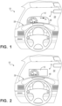
- the electro-optic assembly 10 is utilized in a heads up display system 14 of a vehicle 18.
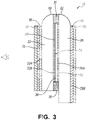
- the electro-optic assembly 10 has a first partially reflective, partially transmissive glass substrate 22 and a second partially reflective, partially transmissive glass substrate 26.
- the first substrate 22 has a first surface 22A and a second surface 22B.
- the second substrate 26 has a third surface 26A and a fourth surface 26B.
- the first and second substrates 22, 26 may be positioned in a parallel spaced-apart relationship and may have a seal 30 disposed around a perimeter of the first and second substrates 22, 26.
- the first substrate 22 and the second substrate 26 define a cavity 34.
- An electro-optic material 38 is disposed in the cavity 34 between the first and second substrates 22, 26.
- the electro-optic assembly 10 is configured to have a non-varying reflectance and a varying transmittance.
- a "clear state" of the electro-optic assembly 10 refers to the condition of maximum transmittance.
- the activation of the electro-optic material 38 may reduce the transmittance of the electro-optic assembly 10 to a "darkened state.”
- the "low end" transmittance refers to the minimum transmittance attainable by the electro-optic assembly 10.
- the electro-optic assembly 10 is included in the heads up display system 14 for the vehicle 18.
- the electro-optic assembly 10 functions as a combiner screen to reflect a primary image projected by a projector 46.
- the electro-optic assembly 10 may be controlled to vary the amount of light transmission based on input from a control circuit. For example, in daylight conditions, the electro-optic assembly 10 may be darkened to improve or increase the contrast ratio and allow for improved visibility of information projected on the electro-optic assembly 10 from the projector 46.
- the contrast ratio may represent the ratio of a primary reflected image from the projector 46 and the light transmitted through the electro-optic assembly 10 (e.g., in either the clear state or the darkened state).
- the heads up display system 14 is capable of use in a variety of applications, such as automotive and aerospace applications, to present information to a driver or pilot while allowing simultaneous forward vision.
- the heads up display system 14 may be provided vehicle rearward of a windscreen 54 and protruding from an instrument panel 58 ( FIG. 1 ), while in other examples, the electro-optic assembly 10 may be positioned directly on the windscreen 54 ( FIG. 2 ).
- the electro-optic assembly 10 may be any size, shape, bend radius, angle, or position.
- the electro-optic assembly 10 may be used to display many vehicle related functions or driver assistance systems, such as alerts, warnings, or vehicle diagnostics. In the depicted examples, the speed of the vehicle 18 is being displayed on the electro-optic assembly 10.
- the image projected onto the electro-optic assembly 10 should be bright enough to see in any condition. This is particularly challenging when the lighting outside the vehicle 18 is bright.
- the contrast between the light from the projector 46 and the lighting behind the electro-optic assembly 10 may be low on a bright sunny day. While a brighter, more intense lighting source (e.g., the projector 46) improves the contrast, increasing the display brightness may not be the most economical solution and a display that is bright enough to provide reasonable contrast in very bright daylight conditions will be too bright in other conditions.
- controls may be used to deal with variations in brightness, the specific background is ever changing in a moving vehicle, and depends, in part, on the position of the eyes of the driver.
- the electro-optic assembly 10 may be configured to lower the transmittance and/or to increase the contrast ratio.
- the initial reflectance and range of transmittance properties is further complicated by the capabilities of the projector 46 employed with the heads up display system 14 and the light output capabilities of the projector 46 along with the light transmittance levels for the windscreen 54.
- the windscreen 54 will have a direct impact on the contrast ratio and visibility of the image from the heads up display system 14. There are a number of factors which affect the transmittance levels of the windscreen 54.
- the minimum light transmittance is based on the rules in the location in which the vehicle 18 is sold but higher transmittance levels may be present based on how the vehicle 18 is equipped and marketed. This range of factors creates the need for solutions that may be adapted to different vehicle and environmental conditions.
- Another aspect that should be considered when utilizing the heads up display system 14 is a secondary reflection from the first through fourth surfaces 22A-26B of the first and second substrates 22, 26. Reflection off of the first through fourth surfaces 22A-26B may create a double image effect from secondary reflections that do not perfectly align with the primary reflected image (e.g., due to geometries of the components of the electro-optic assembly 10). The double image that may be formed from secondary reflections off of the first through fourth surfaces 22A-26B may cause the primary image projected by the projector 46 and reflected by the electro-optic assembly 10 to appear blurry or unclear.
- the electro-optic assembly 10 may be assembled using two approximately 1.6 mm glass substrates (e.g., the first and second substrates 22, 26), which are both bent with a spherical radius of approximately 1250 mm, or other thicknesses for the first and second substrates 22, 26 may be used.
- the first and second substrates 22, 26 may be bent to have a "free-form" shape.
- the desired shape is one in which the resultant primary reflected image "appears" to be forward of the electro-optic assembly 10 and forward of the vehicle 18.
- the exact surface contour needed to attain this characteristic is a function of the properties of the projector 46, the projector 46 and driver location, as well as the electro-optic assembly 10 location, relative to the other two locations.
- the shape of the electro-optic assembly 10 should also be selected so as to preserve the basic characteristics of the projected image (i.e., straight lines remain straight, aspect ratios of images are preserved, etc.).
- each of the first and second substrates 22, 26 include a rounded edge 62 and a contact edge that is not rounded.
- the non-rounded contact edge may be desirable for ease of contact, and if the device is supported by that edge, there would be no need to round the first and second substrates 22, 26 along the contact edge.
- Any exposed edge on the electro-optic assembly 10 may be generally rounded.
- the radius of curvature of the rounded edges 62 may be greater than approximately 2.5 mm.
- the first substrate 22 includes the first surface 22A and the second surface 22B.
- the first surface 22A may be concave and may be coated with chromium (Cr).
- the coated first substrate 22 may have a transmittance of approximately 37.8% and a reflectance of approximately 25.4%.
- the second substrate 26 defines the third and fourth surfaces 26A, 26B.
- the third surface 26A may be coated with indium tin oxide with a sheet resistance of approximately 12 ohms/sq.
- the electro-optic assembly 10 may have a clear state reflectance of approximately 25% and a transmittance of approximately 24%.
- the electro-optic assembly 10 may have a low end, or state, transmittance of approximately 10.5% while maintaining a reflectance from the first surface 22A of approximately 15%.
- the high end, or state, transmittance of the electro-optic assembly 10 may be greater than 45% or even 60%.
- the transmittance of the transflective coating is between about 15% and 50% and the reflectance is between about 10% and 50%.
- the transflective coating of the electro-optic assembly may have a reflectance of between about 15% and 40% and a transmittance between about 20% and 40%.
- the characteristics of the electro-optic assembly 10 may also be altered so that the low end transmittance is less than 7.5% or even less than 5% in the darkened state. In some examples, transmittance levels down to 2.5% or less may be desirable. Increasing the high end transmittance may be obtained by the use of coatings and materials which have low absorption, as will be described herein. Lower low end transmittances may be obtained through the inclusion of materials which have higher absorption. If a wide dynamic range is desired, then low absorption materials may be used in combination with electro-optic materials and cell spacings (e.g., the space between the first and second substrates 22, 26) which attain higher absorbance in the activated state. Those skilled in the art will recognize that there exists a multitude of combinations of coatings and electro-optic materials, cell spacings, and coating conductivity levels that may be selected to attain particular device characteristics.
- electrical elements may be provided on opposing sides of the first and second substrates 22, 26 (e.g., the second and third surfaces 22B, 26A) to generate an electrical potential therebetween.
- a J-clip may be electrically engaged with each electrical element, and electrical element wires extend from the J-clips to a primary printed circuit board.
- the contacts are located along one side of the device. In this example, there is a back plate and top plate offset to allow contact, such as a bus clip. Other contact designs are possible, including the use of conductive ink or epoxy.
- the electro-optic material 38 may be an electrochromic material or medium.
- the electro-optic material 38 may include at least one solvent, at least one anodic material, and at least one cathodic material.
- both of the anodic and cathodic materials are electroactive and at least one of them is electrochromic.
- electrochromic may mean a material that undergoes a modification in its oxidation state upon exposure to a particular electrical potential difference.
- electrochromic means a material that exhibits a change in its extinction coefficient at one or more wavelengths upon exposure to a particular electrical potential difference.
- Electrochromic components include materials whose color or opacity are affected by electric current, such that when an electrical current is applied to the material, the color or opacity change from a first phase to a second phase.
- the electrochromic component may be a single-layer, single-phase component, multi-layer component, or multi-phase component, as described in U.S. Patent Nos.
- the first and second substrates 22, 26 are not limited to glass elements but may also be any other element having partially reflective, partially transmissive properties.
- Other known constructions include U.S. Patent Publication No. 2009/0181203 , which discloses laminated glazed and sealed windows and a peripheral reinforcing means for the same, French Publication No. FR2922328 , which discloses improvements to visual display screens, and U.S. Patent No. 6,700,692 , which discloses an electrochromic rearview mirror assembly that incorporates a display/signal light.
- the electro-optic assembly 10 includes a transflector as well as a variety of other features. More specifically, the electro-optic assembly 10 includes a transflective coating 70, an optional anti-reflection coating 80, and an optional scratch-resistant coating 90.
- the transflective coating 70 is positioned proximate the first surface 22A, and additionally on the second surface 22B.
- the anti-reflection coating 80 is on the first, third and fourth surfaces 22A, 26A, 26B, but it will be understood that the anti-reflection coating 80 may additionally or alternatively be positioned on the second surface 22B without departing from the teachings provided herein.
- the anti-reflection coating 80 is positioned on at least one of the first and second surfaces 22A, 22B, and may be positioned on the first surface 22A, which, according to the claimed invention, is opposite the second surface 22B onto which the transflective coating 70 is positioned.
- the anti-reflection coating 80 on the third surface 26A functions as an electrode (e.g., an anti-reflective electrode) to enable darkening of the electrochromic medium 38.
- the transflective coating 70 located on the second surface 22B serves a dual purpose also acting as an electrode.
- the scratch-resistant coating 90 is positioned proximate the first and fourth surfaces 22A, 26B. It will be understood that although described as separate layers, the transflective coating 70, the anti-reflection coating 80, and/or the scratch-resistant coating 90 may share properties that function as the other coatings, as described in greater detail herein.
- the transflective coating 70 may be a thin metal layer (e.g., a metal-based coating 70), such as Cr or another metal.
- a metal-based coating 70 such as Cr or another metal.
- a potential downside of using a single metal coating layer as the transflective coating 70 is that there is a defined relationship between the reflectance and transmittance which is derived from the thickness of the metal. A single-metal layer does not generally allow for reflectance and transmittance to be independently controlled.
- a low absorption layer including a material of lower absorption than the metal, such as indium tin oxide (ITO) or a dielectric material, is located in between the substrate (e.g., the first substrate 22) and the metal coating layer.
- the transflective coating 70 may be located on either the first surface 22A or the second surface 22B.
- FIG. 6 compares the attainable transmittance and corresponding reflectance values for an electro-optic assembly 10 with a single Cr layer versus a bilayer of ITO (70 nanometers (nm) thick, next to glass) and Cr (e.g., the transflective coating 70) on the first surface 22A for different values of the Cr layer thickness.
- the coatings on the second surface 22B and the third surface 26A are composed of 115 nm thick ITO, and the fourth surface 26B is coated with a thin chromium layer.
- the addition of a low absorption layer, such as ITO, increases the range of attainable reflectance and transmittance values for the transflective coating 70 by making it possible to tune the reflectance and reflected color independent of the thickness and the refractive index.
- the thickness of the low absorption layer which may include a dielectric material, may be between from about 5 to 240 nm, or between about 10 and 120 nm or between 20 and 100 nm.
- the refractive index of the low absorption layer may be greater than about 1.3.
- the reflected color may also be tuned slightly by increasing or decreasing the thickness of the low absorption layer.
- the metal layer may be selected from the metal list provided below and the material of the low absorption layer may be selected from the list of dielectric materials provided below which meet the refractive index properties for this example.
- the comparative example of the transflective coating 70 having a dielectric-metal bilayer provides a higher range of attainable values for reflectance and transmittance than a single metallic layer, it still may be a challenge to tune the refractive index and absorption of the materials to achieve a particular reflectance and transmittance level. Therefore, it may be advantageous to have a transflective coating 70 that allows more flexibility in terms of reflectance and transmittance values, especially when lower transmittance values are sought. Accordingly, in another comparative example of the transflective coating 70, such characteristics may be obtained with a multi-layer coating, such as a metal/dielectric/metal structure (MDM), which may be used as either a first surface or a second surface transflective coating.
- MDM metal/dielectric/metal structure
- an M-layer of the MDM coating includes one or more of chromium, molybdenum, nickel, Inconel, indium, palladium, osmium, tungsten, rhenium, iridium, rhodium, ruthenium, stainless steel, tantalum, titanium, copper, gold, platinum, any other platinum group metals, zirconium, vanadium AlSi alloys, and alloys, and/or combinations thereof. It will be understood that any of the aforementioned metals may be utilized for the single or bilayer examples of the transflective coating 70. In some examples, combinations of metals and dielectric materials may depend on whether the transflective coating 70 is configured on the first surface 22A for durability or electrode properties.
- the dielectric material may be selected from one or more of the following: ITO, SnO 2 , SiN, MgF 2 , SiO 2 , TiO 2 , F:SnO 2 , NbO x , TaOx, indium zinc oxide, aluminum zinc oxide, zinc oxide, electrically conductive TiO 2 , CeOx, ZnS, chromium oxide, ZrO x , WO 3 , nickel oxide, IrO 2 , NiO x , CrO x , NbO x , and ZrO x , or other material with a refractive index between about 1.37 and about 4. It will be understood that any of the aforementioned dielectrics may be utilized for the bilayer example of the transflective coating 70.
- FIG. 7 depicts the reflectance and transmittance values for a multi-layer transflective structure (e.g., the transflective coating 70) with a Cr/ITO/Cr structure, where the ITO thickness is 74.7 nm.
- Each point denotes a particular reflectance/transmittance (R/T) value for a combination of 1 st and 2 nd Cr layer thicknesses. It is possible to see that these two parameters span a range of transmittance values for a particular reflectance and it is possible to control reflectance and transmittance separately in this range.
- the relationship between the metal layers will change as the thickness and index of the middle low absorption layer changes. Similarly, the reflectance and transmittance values will shift as different metals and dielectric layers are used.
- the reflectance of the MDM stack may be between about 10 to 50%, or may be between about 15 to 40%, or may be between about 20 and 35%.
- the transmittance may be between about 15 and 50%, or may be between about 20 and 40%, or may be between about 25 and 35%.
- the thickness of the metal layers may be between about 0.1 to 10 nm, or between about 0.2 and 5 nm, or between about 0.3 and 2.5 nm.
- the thickness of the dielectric layer may be between from about 5 to 240 nm, or between about 10 and 120 nm or between about 20 and 100 nm.
- an undercoat metallic layer may be positioned between the first substrate and the dielectric layer.
- the selection of metal will also shift the illustrated relationships.
- two different metals may be selected for the top and bottom M-layers and the D-layer may be further subdivided into sub-layers and include materials of different refractive indices.
- Additional D- and/or M-layers may be added without deviating from the teachings provided herein.
- the additional layers may be added to improve durability, adhesion, or alter the color and/or reflectance and transmittance ranges or robustness.
- TCOs transparent conductive oxides
- DLC diamond-like carbon
- the transflective coating 70 on the second surface 22B functions as the electrode for the electrochromic media.
- the transflective coating 70 in this embodiment, may have a sheet resistance less than about 20 ohms/sq, less than about 15 ohms/sq, less than about 10 ohms/sq, or less than about 5 ohms/sq.
- the transflector to be compatible with the electrochromic media, may include an electrically conductive layer adjacent to the electrochromic media.
- a transflector on the second surface 22B which has surface isolation from the environment, enables use of metals and materials that are not environmentally durable.
- silver based alloys may now be used in the transflector layer.
- the optical properties of silver and its alloys has another useful characteristic - lower absorption.
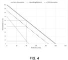
- FIG. 4 illustrates the reflectance and transmittance relationship of a silver coating for different thicknesses. As understood from FIG. 4 , the absorption, which equals 100% minus the reflectance and transmittance, may be calculated. Further, as illustrated in FIG. 4 , the absorption is approximately 13-15%. The use of a silver layer in a transflective coating will therefore enable a broader combination of attainable reflectance and transmittance attributes.
- FIG. 4 the theoretically attainable reflectance and transmittance of a system with zero absorption is generally illustrated.
- the area to the upper right of the zero absorption line is generally not attainable since the sum of reflectance, transmittance, and absorption has to equal 100%.
- the area to the lower left of the zero absorption line is attainable through the use of absorbing materials as part of the electro-optic assembly 10 or the transflective coating 70.
- the reflectance and transmittance relationship of a silver based coating with an assumed 15% absorption is shown in FIG. 4 , along with the reflectance and transmittance relationship of an absorbing metal.
- the zone between these two lines is the additional region enabled by the inclusion of a silver based layer to the transflector stack.
- FIG. 4 also shows the attainable transmittance of the different options for a 40% reflector.
- the range of allowable transmittance is approximately four times larger for the silver based transflector compared to the absorbing metal transflector.
- the allowable combination of reflectance and transmittance for the electro-optic assembly 10 including a silver based transflector may be selected such that the reflectance plus transmittance (R+T) ⁇ 90%. However, other silver based transflectors may have (R+T) values of less than 80% or even less than 70% or 60%.
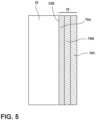
- the transflective coating 70 is disposed on the second surface 22B of the substrate 22.
- the transflective coating 70 is sub-divided into three sub-layers. It should be understood that the novel silver based transflector is not limited to a three-layer stack. Additional sub-layers may be present and within the scope of the claimed invention.
- the three-layer stack is presented to allow description of the optional functions of the additional layers.
- the reflectance of the transflective coating 70 is greater than about 20%, may be greater than about 30%, or may be greater than about 40%.
- a silver based conductive layer 70B has a thickness that may vary from about 2 nm to 30 nm, or alternatively between about 6 nm to 15 nm.
- the silver based layer 70B may also be subdivided or be comprised of alloys.
- Useful additions to the silver material may include, but are not limited to, gold, palladium, platinum, rhodium, titanium, aluminum, zinc, copper, tin, silicon, germanium, manganese, magnesium, tungsten, lead, boron, chrome, thorium, tantalum, lithium, and indium.
- a base layer 70A includes at least one of a dielectric, TCO, or a noble metal layer.
- the base layer 70A may be used to help adhesion or tune reflectance and/or transmittance.
- TCO materials may be selected from the list that includes ITO, F:Sn02, Sb:Sn02, Doped ZnO such as AI:ZnO, Ga:ZnO, B:ZnO, IZO, and Nb:Ti02.
- the dielectrics may be selected from the group described for the MDM structure.
- the metals suitable for the base layer 70A may also be selected from the group detailed above. As the thickness of the silver layer is increased to increase the conductivity and lower the sheet resistance, the reflectance will be increased.
- the base layer 70A may be tuned to adjust the reflectance and transmittance intensity and/or color of the transflective coating 70.
- An overcoat layer 70C may include a platinum group metal, such as ruthenium, rhodium, platinum, palladium, osmium, or iridium. This type of material will be compatible with the electrochromic media, while providing at least one of increased conductivity (lower sheet resistance), reflectance tuning, transmittance tuning, or both, or higher color rendering index (CRI) values.
- the overcoat layer 70C is disposed between the electro-optic material and the silver conductive layer.
- the overcoat layer 70C includes a noble metal.
- the transflective coating 70 may include any of the transflective coatings and layers disclosed in U.S. Provisional Patent Application No. 62/205,376, filed on August 14, 2015 , entitled “ELECTRO-OPTIC ASSEMBLY,” Attorney Docket Nos. AUTO 02215US (GEN010 P917A), entitled “ELECTRO-OPTIC ELEMENT WITH IMI LAYER,” and AUTO 02214US (GEN010 P918A), entitled “ELECTRO-OPTIC ELEMENT WITH HIGH DOUBLE IMAGE RATIO,”.
- the primary reflectance of the heads up display system 14 comes from the transflective coating 70 located on the second surface 22B of the electro-optic assembly 10, it is generally important to minimize secondary reflections from the other surfaces (e.g., the first, third and fourth surfaces 22A, 26A, 26B where the transflective coating 70 is not present), which may result in a blurry image (i.e., double imaging). Accordingly, use of the anti-reflection coatings 80 may be advantageous.
- An example of the anti-reflection coating 80 may be a transparent conductive oxide.
- the third surface 26A may include a transparent electrode.
- Transparent conductive oxides such as ITO, F:SnO 2 , doped-ZnO, IZO, or other layers
- TCO Transparent conductive oxides
- the reflectance of these materials is a function of the thickness of the coatings due to interference effects.
- a minimum reflectance may be obtained by tailoring the thickness of the conductive oxide coating (e.g., the anti-reflection coating 80).
- the minimum reflectance is at a half wave optical thickness.
- the wavelength for the half wave condition may be adjusted to get the net lowest reflectance value.
- a reflectance of an ITO coating may be as low as, or lower than, 0.5% from the third surface 26A with a layer about 145 nm thick of the anti-reflection coating 80.
Claims (7)
- Système d'affichage tête haute (14) pour un véhicule (18) comprenant un ensemble électro-optique (10), l'ensemble électro-optique (10) étant un écran combineur destiné au système d'affichage tête haute (14) et étant conçu pour réfléchir une image projetée vers une première surface (22A) à l'aide d'un projecteur (46),
l'ensemble électro-optique (10) comprenant :un premier substrat (22) partiellement réfléchissant, partiellement transmissif, définissant la première surface (22A) et une deuxième surface (22B) ;un second substrat (26) partiellement réfléchissant, partiellement transmissif, définissant une troisième surface (26A) et une quatrième surface (26B) ;un espace (34) défini entre la deuxième surface (22B) et la troisième surface (26A) ;un matériau électro-optique (38) disposé entre la deuxième surface (22B) du premier substrat (22) et la troisième surface (26A) du second substrat (26), ledit ensemble électro-optique (10) permettant de modifier un état de transmittance soit de manière distincte, soit de manière continue ;un revêtement transflectif (70) disposé sur la deuxième surface (22B), le revêtement transflectif (70) comprenant une couche de finition (70C), une couche conductrice en argent (70B) et une couche de base (70A) comprenant un oxyde conducteur transparent (TCO) et/ou un matériau diélectrique et/ou un métal noble, la couche de finition (70C) étant disposée entre le matériau électro-optique (38) et la couche conductrice en argent (70B), et la couche de base (70A) étant disposée entre la couche conductrice en argent (70B) et le premier substrat (22),caractérisé en ce quela couche de finition (70C) comprend un métal noble. - Le système d'affichage tête haute (14) de la revendication 1, dans lequel la couche de finition (70C) comprend un métal du groupe du platine.
- Le système d'affichage tête haute (14) de l'une quelconque des revendications 1-2, dans lequel la somme du pouvoir réflecteur et de la transmittance du revêtement transflectif (70) est inférieure à environ 80 %.
- Le système d'affichage tête haute (14) de l'une quelconque des revendications 1-3, dans lequel une épaisseur de la couche conductrice en argent (70B) est comprise entre environ 2 nm et 30 nm.
- Le système d'affichage tête haute (14) de l'une quelconque des revendications 1-4, dans lequel un pouvoir réflecteur du revêtement transflectif (70) est supérieur à environ 20 %.
- Le système d'affichage tête haute (14) de l'une quelconque des revendications 1-5, dans lequel le matériau électro-optique (38) est un matériau électro-chromique.
- Le système d'affichage tête haute (14) de l'une quelconque des revendications 1-6, dans lequel une valeur de résistance de couche du revêtement transflectif (70) est inférieure à environ 20 ohms/carré.
Applications Claiming Priority (2)
| Application Number | Priority Date | Filing Date | Title |
|---|---|---|---|
| US201662363038P | 2016-07-15 | 2016-07-15 | |
| PCT/US2017/042165 WO2018013941A1 (fr) | 2016-07-15 | 2017-07-14 | Transflecteur placé sur une deuxième surface pour dispositif électro-optique |
Publications (3)
| Publication Number | Publication Date |
|---|---|
| EP3452318A1 EP3452318A1 (fr) | 2019-03-13 |
| EP3452318A4 EP3452318A4 (fr) | 2019-06-05 |
| EP3452318B1 true EP3452318B1 (fr) | 2023-03-08 |
Family
ID=60940577
Family Applications (1)
| Application Number | Title | Priority Date | Filing Date |
|---|---|---|---|
| EP17828543.3A Active EP3452318B1 (fr) | 2016-07-15 | 2017-07-14 | Affichage tête haute comprenant un ensemble électro-optique |
Country Status (6)
| Country | Link |
|---|---|
| US (1) | US10234720B2 (fr) |
| EP (1) | EP3452318B1 (fr) |
| JP (1) | JP7005589B2 (fr) |
| KR (1) | KR102530960B1 (fr) |
| CN (1) | CN109476218B (fr) |
| WO (1) | WO2018013941A1 (fr) |
Families Citing this family (5)
| Publication number | Priority date | Publication date | Assignee | Title |
|---|---|---|---|---|
| DE112019000701T5 (de) * | 2018-02-07 | 2020-10-22 | AGC Inc. | Laminiertes Glas |
| CN109782506B (zh) * | 2019-01-10 | 2021-08-03 | 上海理工大学 | 一种光学可变玻璃及光学可变悬浮展示装置 |
| CN114341722B (zh) * | 2019-09-11 | 2023-12-08 | 金泰克斯公司 | 抗反射电极 |
| US11465468B2 (en) | 2019-12-18 | 2022-10-11 | Gentex Corporation | Window overmold |
| JP7411889B2 (ja) * | 2020-03-27 | 2024-01-12 | パナソニックIpマネジメント株式会社 | 表示装置および制御回路 |
Family Cites Families (36)
| Publication number | Priority date | Publication date | Assignee | Title |
|---|---|---|---|---|
| US697499A (en) | 1901-09-28 | 1902-04-15 | Charles Wm Kromenaker | Book-holder. |
| GB2269681B (en) * | 1992-07-14 | 1995-06-07 | Yazaki Corp | Display system for vehicles |
| DE19605451A1 (de) | 1996-02-15 | 1997-08-21 | Bayer Ag | Elektrochromes System |
| US5928572A (en) | 1996-03-15 | 1999-07-27 | Gentex Corporation | Electrochromic layer and devices comprising same |
| JPH10115802A (ja) * | 1996-10-11 | 1998-05-06 | Central Glass Co Ltd | 表示装置 |
| US5998617A (en) | 1997-04-02 | 1999-12-07 | Gentex Corporation | Electrochromic compounds |
| US6700692B2 (en) | 1997-04-02 | 2004-03-02 | Gentex Corporation | Electrochromic rearview mirror assembly incorporating a display/signal light |
| US6020987A (en) | 1997-04-02 | 2000-02-01 | Gentex Corporation | Electrochromic medium capable of producing a pre-selected color |
| US6141137A (en) | 1998-08-26 | 2000-10-31 | Gentex Corporation | Electrochromic media for producing a preselected color |
| US6193912B1 (en) | 1998-03-03 | 2001-02-27 | Gentex Corporation | Near infrared-absorbing electrochromic compounds and devices comprising same |
| KR20010102154A (ko) | 1999-02-18 | 2001-11-15 | 오오자와 슈지로 | 전기착색 소자 |
| US6137620A (en) | 1999-04-30 | 2000-10-24 | Gentex Corporation | Electrochromic media with concentration-enhanced stability, process for the preparation thereof and use in electrochromic devices |
| US6816297B1 (en) * | 1999-06-25 | 2004-11-09 | Gentex Corporation | Electrochromic mirror having a self-cleaning hydrophilic coating |
| US6249369B1 (en) | 1999-07-09 | 2001-06-19 | Gentex Corporation | Coupled electrochromic compounds with photostable dication oxidation states |
| US6561460B2 (en) * | 2000-08-03 | 2003-05-13 | Ppg Industries Ohio, Inc. | Switchable electrochromic devices for use in aircraft transparency windows |
| ES2287266T3 (es) * | 2001-01-23 | 2007-12-16 | Donnelly Corporation | Sistema de iluminacion de vehiculos mejorado. |
| US7255451B2 (en) * | 2002-09-20 | 2007-08-14 | Donnelly Corporation | Electro-optic mirror cell |
| US6654070B1 (en) | 2001-03-23 | 2003-11-25 | Michael Edward Rofe | Interactive heads up display (IHUD) |
| US6655806B2 (en) * | 2001-11-20 | 2003-12-02 | Marigen Company Ltd. | Automotive optical lens sun shield |
| US7374290B2 (en) * | 2003-06-13 | 2008-05-20 | Sony Corporation | Projection type display device |
| EP2426552A1 (fr) | 2006-03-03 | 2012-03-07 | Gentex Corporation | Éléments électro-optiques incorporant des revêtements améliorés à couche mince |
| FR2899631B1 (fr) * | 2006-04-10 | 2010-02-26 | Saint Gobain | Vitrage feuillete et ses moyens d'etancheification et de renforcement peripherique |
| US7893890B2 (en) | 2007-03-05 | 2011-02-22 | The Boeing Company | Electrically dimmable combiner optics for head-up display |
| FR2922328B1 (fr) * | 2007-10-12 | 2009-11-27 | Saint Gobain | Perfectionnements apportes a des ecrans de visualisation |
| JP2009122582A (ja) * | 2007-11-19 | 2009-06-04 | Fujinon Corp | 投影光学系及びヘッドアップディスプレイ装置 |
| US7864431B2 (en) * | 2008-06-04 | 2011-01-04 | Centre Luxembourgeois De Recherches Pour Le Verre Et La Ceramique S.A. (C.R.V.C.) | Windshield for use with head-up display and/or method of making the same |
| FR2948356B1 (fr) * | 2009-07-22 | 2011-08-19 | Saint Gobain | Dispositif electrochrome |
| US8988755B2 (en) * | 2011-05-13 | 2015-03-24 | Magna Mirrors Of America, Inc. | Mirror reflective element |
| US9805570B2 (en) | 2011-06-22 | 2017-10-31 | Garrett Thermal Systems Limited | Particle detector with dust rejection |
| CN102442252A (zh) * | 2011-12-16 | 2012-05-09 | 重庆市科学技术研究院 | 一种车载平视投影显示设备 |
| US9606409B2 (en) * | 2013-09-13 | 2017-03-28 | Itn Energy Systems Inc. | Electrochromic window insert assembly and methods of manufacture |
| CN104570535A (zh) * | 2013-10-24 | 2015-04-29 | 力光兴科技股份有限公司 | 电致变色汽车后视镜体结构及其制造方法 |
| US10054836B2 (en) * | 2014-11-21 | 2018-08-21 | Gentex Corporation | Electro-optic assembly |
| US9878669B2 (en) * | 2015-02-24 | 2018-01-30 | Magna Mirrors Of America, Inc. | Mirror assembly with spring-loaded electrical connectors |
| US10766422B2 (en) * | 2015-12-11 | 2020-09-08 | Gentex Corporation | IR transmitting coating for electro-optic element |
| WO2018156918A1 (fr) * | 2017-02-27 | 2018-08-30 | Gentex Corporation | Revêtements transflectif pour transparents |
-
2017
- 2017-07-14 EP EP17828543.3A patent/EP3452318B1/fr active Active
- 2017-07-14 WO PCT/US2017/042165 patent/WO2018013941A1/fr unknown
- 2017-07-14 CN CN201780042576.6A patent/CN109476218B/zh active Active
- 2017-07-14 JP JP2019501999A patent/JP7005589B2/ja active Active
- 2017-07-14 US US15/650,540 patent/US10234720B2/en active Active
- 2017-07-14 KR KR1020187036141A patent/KR102530960B1/ko active IP Right Grant
Also Published As
| Publication number | Publication date |
|---|---|
| CN109476218B (zh) | 2023-01-31 |
| WO2018013941A1 (fr) | 2018-01-18 |
| EP3452318A1 (fr) | 2019-03-13 |
| EP3452318A4 (fr) | 2019-06-05 |
| KR102530960B1 (ko) | 2023-05-09 |
| US20180017830A1 (en) | 2018-01-18 |
| KR20190025832A (ko) | 2019-03-12 |
| CN109476218A (zh) | 2019-03-15 |
| JP2019527647A (ja) | 2019-10-03 |
| US10234720B2 (en) | 2019-03-19 |
| JP7005589B2 (ja) | 2022-02-04 |
Similar Documents
| Publication | Publication Date | Title |
|---|---|---|
| US10101583B2 (en) | Heads up display system | |
| EP3452318B1 (fr) | Affichage tête haute comprenant un ensemble électro-optique | |
| US10444575B2 (en) | Electro-optic element with IMI layer | |
| US8035881B2 (en) | Multi-zone mirrors | |
| US10247995B2 (en) | Electro-optic element with high double image ratio | |
| US9274394B2 (en) | Multi-zone mirrors | |
| US11029519B2 (en) | Antireflection coatings | |
| US20120026570A1 (en) | Multi-zone mirrors | |
| CN217099837U (zh) | 一种红外高透防眩目汽车后视镜镜片元件 | |
| CN214299895U (zh) | 一种电致变色防眩目后视镜镜片元件 | |
| US10746910B2 (en) | Transflective coatings for transparencies | |
| CN219927574U (zh) | 后视组件和构件 | |
| CN215204670U (zh) | 一种电致变色后视镜镜片元件及电致变色后视镜组合件 | |
| CN214215624U (zh) | 一种电致变色防眩目后视镜组件 | |
| CN117799400A (zh) | 挡风窗、制造方法、显示装置和交通设备 |
Legal Events
| Date | Code | Title | Description |
|---|---|---|---|
| STAA | Information on the status of an ep patent application or granted ep patent |
Free format text: STATUS: THE INTERNATIONAL PUBLICATION HAS BEEN MADE |
|
| PUAI | Public reference made under article 153(3) epc to a published international application that has entered the european phase |
Free format text: ORIGINAL CODE: 0009012 |
|
| STAA | Information on the status of an ep patent application or granted ep patent |
Free format text: STATUS: REQUEST FOR EXAMINATION WAS MADE |
|
| 17P | Request for examination filed |
Effective date: 20181206 |
|
| AK | Designated contracting states |
Kind code of ref document: A1 Designated state(s): AL AT BE BG CH CY CZ DE DK EE ES FI FR GB GR HR HU IE IS IT LI LT LU LV MC MK MT NL NO PL PT RO RS SE SI SK SM TR |
|
| AX | Request for extension of the european patent |
Extension state: BA ME |
|
| A4 | Supplementary search report drawn up and despatched |
Effective date: 20190503 |
|
| RIC1 | Information provided on ipc code assigned before grant |
Ipc: G02F 1/153 20060101ALI20190426BHEP Ipc: G02B 27/01 20060101AFI20190426BHEP |
|
| DAV | Request for validation of the european patent (deleted) | ||
| DAX | Request for extension of the european patent (deleted) | ||
| STAA | Information on the status of an ep patent application or granted ep patent |
Free format text: STATUS: EXAMINATION IS IN PROGRESS |
|
| 17Q | First examination report despatched |
Effective date: 20200421 |
|
| STAA | Information on the status of an ep patent application or granted ep patent |
Free format text: STATUS: EXAMINATION IS IN PROGRESS |
|
| REG | Reference to a national code |
Ref country code: DE Ref legal event code: R079 Ref document number: 602017066685 Country of ref document: DE Free format text: PREVIOUS MAIN CLASS: B60J0003040000 Ipc: G02B0027010000 |
|
| GRAP | Despatch of communication of intention to grant a patent |
Free format text: ORIGINAL CODE: EPIDOSNIGR1 |
|
| STAA | Information on the status of an ep patent application or granted ep patent |
Free format text: STATUS: GRANT OF PATENT IS INTENDED |
|
| RIC1 | Information provided on ipc code assigned before grant |
Ipc: B32B 17/10 20060101ALN20221007BHEP Ipc: G02B 1/14 20150101ALN20221007BHEP Ipc: G02B 1/11 20150101ALN20221007BHEP Ipc: G02F 1/153 20060101ALI20221007BHEP Ipc: G02B 27/01 20060101AFI20221007BHEP |
|
| INTG | Intention to grant announced |
Effective date: 20221031 |
|
| GRAS | Grant fee paid |
Free format text: ORIGINAL CODE: EPIDOSNIGR3 |
|
| GRAA | (expected) grant |
Free format text: ORIGINAL CODE: 0009210 |
|
| STAA | Information on the status of an ep patent application or granted ep patent |
Free format text: STATUS: THE PATENT HAS BEEN GRANTED |
|
| AK | Designated contracting states |
Kind code of ref document: B1 Designated state(s): AL AT BE BG CH CY CZ DE DK EE ES FI FR GB GR HR HU IE IS IT LI LT LU LV MC MK MT NL NO PL PT RO RS SE SI SK SM TR |
|
| REG | Reference to a national code |
Ref country code: GB Ref legal event code: FG4D |
|
| REG | Reference to a national code |
Ref country code: CH Ref legal event code: EP Ref country code: AT Ref legal event code: REF Ref document number: 1552984 Country of ref document: AT Kind code of ref document: T Effective date: 20230315 |
|
| REG | Reference to a national code |
Ref country code: IE Ref legal event code: FG4D |
|
| REG | Reference to a national code |
Ref country code: DE Ref legal event code: R096 Ref document number: 602017066685 Country of ref document: DE |
|
| P01 | Opt-out of the competence of the unified patent court (upc) registered |
Effective date: 20230503 |
|
| REG | Reference to a national code |
Ref country code: LT Ref legal event code: MG9D |
|
| REG | Reference to a national code |
Ref country code: NL Ref legal event code: MP Effective date: 20230308 |
|
| PG25 | Lapsed in a contracting state [announced via postgrant information from national office to epo] |
Ref country code: RS Free format text: LAPSE BECAUSE OF FAILURE TO SUBMIT A TRANSLATION OF THE DESCRIPTION OR TO PAY THE FEE WITHIN THE PRESCRIBED TIME-LIMIT Effective date: 20230308 Ref country code: NO Free format text: LAPSE BECAUSE OF FAILURE TO SUBMIT A TRANSLATION OF THE DESCRIPTION OR TO PAY THE FEE WITHIN THE PRESCRIBED TIME-LIMIT Effective date: 20230608 Ref country code: LV Free format text: LAPSE BECAUSE OF FAILURE TO SUBMIT A TRANSLATION OF THE DESCRIPTION OR TO PAY THE FEE WITHIN THE PRESCRIBED TIME-LIMIT Effective date: 20230308 Ref country code: LT Free format text: LAPSE BECAUSE OF FAILURE TO SUBMIT A TRANSLATION OF THE DESCRIPTION OR TO PAY THE FEE WITHIN THE PRESCRIBED TIME-LIMIT Effective date: 20230308 Ref country code: HR Free format text: LAPSE BECAUSE OF FAILURE TO SUBMIT A TRANSLATION OF THE DESCRIPTION OR TO PAY THE FEE WITHIN THE PRESCRIBED TIME-LIMIT Effective date: 20230308 Ref country code: ES Free format text: LAPSE BECAUSE OF FAILURE TO SUBMIT A TRANSLATION OF THE DESCRIPTION OR TO PAY THE FEE WITHIN THE PRESCRIBED TIME-LIMIT Effective date: 20230308 |
|
| PGFP | Annual fee paid to national office [announced via postgrant information from national office to epo] |
Ref country code: FR Payment date: 20230621 Year of fee payment: 7 |
|
| REG | Reference to a national code |
Ref country code: AT Ref legal event code: MK05 Ref document number: 1552984 Country of ref document: AT Kind code of ref document: T Effective date: 20230308 |
|
| PG25 | Lapsed in a contracting state [announced via postgrant information from national office to epo] |
Ref country code: SE Free format text: LAPSE BECAUSE OF FAILURE TO SUBMIT A TRANSLATION OF THE DESCRIPTION OR TO PAY THE FEE WITHIN THE PRESCRIBED TIME-LIMIT Effective date: 20230308 Ref country code: NL Free format text: LAPSE BECAUSE OF FAILURE TO SUBMIT A TRANSLATION OF THE DESCRIPTION OR TO PAY THE FEE WITHIN THE PRESCRIBED TIME-LIMIT Effective date: 20230308 Ref country code: GR Free format text: LAPSE BECAUSE OF FAILURE TO SUBMIT A TRANSLATION OF THE DESCRIPTION OR TO PAY THE FEE WITHIN THE PRESCRIBED TIME-LIMIT Effective date: 20230609 Ref country code: FI Free format text: LAPSE BECAUSE OF FAILURE TO SUBMIT A TRANSLATION OF THE DESCRIPTION OR TO PAY THE FEE WITHIN THE PRESCRIBED TIME-LIMIT Effective date: 20230308 |
|
| PG25 | Lapsed in a contracting state [announced via postgrant information from national office to epo] |
Ref country code: SM Free format text: LAPSE BECAUSE OF FAILURE TO SUBMIT A TRANSLATION OF THE DESCRIPTION OR TO PAY THE FEE WITHIN THE PRESCRIBED TIME-LIMIT Effective date: 20230308 Ref country code: RO Free format text: LAPSE BECAUSE OF FAILURE TO SUBMIT A TRANSLATION OF THE DESCRIPTION OR TO PAY THE FEE WITHIN THE PRESCRIBED TIME-LIMIT Effective date: 20230308 Ref country code: PT Free format text: LAPSE BECAUSE OF FAILURE TO SUBMIT A TRANSLATION OF THE DESCRIPTION OR TO PAY THE FEE WITHIN THE PRESCRIBED TIME-LIMIT Effective date: 20230710 Ref country code: EE Free format text: LAPSE BECAUSE OF FAILURE TO SUBMIT A TRANSLATION OF THE DESCRIPTION OR TO PAY THE FEE WITHIN THE PRESCRIBED TIME-LIMIT Effective date: 20230308 Ref country code: CZ Free format text: LAPSE BECAUSE OF FAILURE TO SUBMIT A TRANSLATION OF THE DESCRIPTION OR TO PAY THE FEE WITHIN THE PRESCRIBED TIME-LIMIT Effective date: 20230308 Ref country code: AT Free format text: LAPSE BECAUSE OF FAILURE TO SUBMIT A TRANSLATION OF THE DESCRIPTION OR TO PAY THE FEE WITHIN THE PRESCRIBED TIME-LIMIT Effective date: 20230308 |
|
| PGFP | Annual fee paid to national office [announced via postgrant information from national office to epo] |
Ref country code: GB Payment date: 20230620 Year of fee payment: 7 |
|
| PG25 | Lapsed in a contracting state [announced via postgrant information from national office to epo] |
Ref country code: SK Free format text: LAPSE BECAUSE OF FAILURE TO SUBMIT A TRANSLATION OF THE DESCRIPTION OR TO PAY THE FEE WITHIN THE PRESCRIBED TIME-LIMIT Effective date: 20230308 Ref country code: PL Free format text: LAPSE BECAUSE OF FAILURE TO SUBMIT A TRANSLATION OF THE DESCRIPTION OR TO PAY THE FEE WITHIN THE PRESCRIBED TIME-LIMIT Effective date: 20230308 Ref country code: IS Free format text: LAPSE BECAUSE OF FAILURE TO SUBMIT A TRANSLATION OF THE DESCRIPTION OR TO PAY THE FEE WITHIN THE PRESCRIBED TIME-LIMIT Effective date: 20230708 |
|
| PGFP | Annual fee paid to national office [announced via postgrant information from national office to epo] |
Ref country code: DE Payment date: 20230620 Year of fee payment: 7 |
|
| REG | Reference to a national code |
Ref country code: DE Ref legal event code: R097 Ref document number: 602017066685 Country of ref document: DE |
|
| PLBE | No opposition filed within time limit |
Free format text: ORIGINAL CODE: 0009261 |
|
| STAA | Information on the status of an ep patent application or granted ep patent |
Free format text: STATUS: NO OPPOSITION FILED WITHIN TIME LIMIT |
|
| PG25 | Lapsed in a contracting state [announced via postgrant information from national office to epo] |
Ref country code: SI Free format text: LAPSE BECAUSE OF FAILURE TO SUBMIT A TRANSLATION OF THE DESCRIPTION OR TO PAY THE FEE WITHIN THE PRESCRIBED TIME-LIMIT Effective date: 20230308 Ref country code: DK Free format text: LAPSE BECAUSE OF FAILURE TO SUBMIT A TRANSLATION OF THE DESCRIPTION OR TO PAY THE FEE WITHIN THE PRESCRIBED TIME-LIMIT Effective date: 20230308 |
|
| 26N | No opposition filed |
Effective date: 20231211 |
|
| PG25 | Lapsed in a contracting state [announced via postgrant information from national office to epo] |
Ref country code: MC Free format text: LAPSE BECAUSE OF FAILURE TO SUBMIT A TRANSLATION OF THE DESCRIPTION OR TO PAY THE FEE WITHIN THE PRESCRIBED TIME-LIMIT Effective date: 20230308 |
|
| PG25 | Lapsed in a contracting state [announced via postgrant information from national office to epo] |
Ref country code: MC Free format text: LAPSE BECAUSE OF FAILURE TO SUBMIT A TRANSLATION OF THE DESCRIPTION OR TO PAY THE FEE WITHIN THE PRESCRIBED TIME-LIMIT Effective date: 20230308 |
|
| REG | Reference to a national code |
Ref country code: CH Ref legal event code: PL |
|
| PG25 | Lapsed in a contracting state [announced via postgrant information from national office to epo] |
Ref country code: LU Free format text: LAPSE BECAUSE OF NON-PAYMENT OF DUE FEES Effective date: 20230714 |
|
| PG25 | Lapsed in a contracting state [announced via postgrant information from national office to epo] |
Ref country code: LU Free format text: LAPSE BECAUSE OF NON-PAYMENT OF DUE FEES Effective date: 20230714 |